Article

Effect of Oxygen Content on Current Stress-Induced Instability in Bottom-Gate Amorphous InGaZnO Thin-Film Transistors

The School of Electrical Engineering, Kookmin University, Seoul 02707, Korea
*
Author to whom correspondence should be addressed.
Materials 2019, 12(19), 3149; https://doi.org/10.3390/ma12193149
Submission received: 10 August 2019 / Revised: 18 September 2019 / Accepted: 24 September 2019 / Published: 26 September 2019
(This article belongs to the Section Thin Films and Interfaces)

Abstract

:
The effect of oxygen content on current-stress-induced instability was investigated in bottom-gate amorphous InGaZnO (a-IGZO) thin-film transistors. The observed positive threshold voltage shift (ΔVT) was dominated by electron trapping in the gate insulator (GI), whereas it was compensated by donor creation in a-IGZO active regions when both current flows and a high lateral electric field were present. Stress-induced ΔVT increased with increasing oxygen content irrespective of the type of stress because oxygen content influenced GI quality, i.e., higher density of GI electron traps, as well as typical direct current (DC) performance like threshold voltage, mobility, and subthreshold swing. It was also found that self-heating became another important mechanism, especially when the vertical electric field and channel current were the same, independent of the oxygen content. The increased ΔVT with oxygen content under positive gate bias stress, positive gate and drain bias stress, and target current stress was consistently explained by considering a combination of the density of GI electron traps, electric field relaxation, and self-heating-assisted electron trapping.

1. Introduction

Since amorphous InGaZnO (a-IGZO) thin-film transistors (TFTs) are used in active-matrix organic light-emitting diode (AMOLED) television manufacturing, their reliability under long-term current stress is an important and challenging issue [1]. Although a-IGZO TFTs have been successfully commercialized into display products, next-generation displays with higher resolution, higher brightness, and longer product lifetime will demand more stable device characteristics. In particular, current stress-induced instability must be analyzed systematically along with various bias conditions, i.e., various gate-to-source voltage (VGS) and drain-to-source voltage (VDS) conditions, because current-driving TFTs in an AMOLED pixel as well as the TFTs in gate-driver circuitry experience various VGS and VDS conditions during real operation of the display circuits. On the other hand, the performance or stability of a-IGZO TFTs has been widely designed and optimized based on controlling the oxygen content (O-content) in IGZO thin films [2,3,4,5,6,7,8]. Therefore, thoroughly understanding the effect of O-content in IGZO thin films on current stress (CS)-induced instability under various VGS and VDS conditions is indispensable for the design of highly stable a-IGZO TFTs as well as for the design of current-driving schemes for high frame-rate display backplanes [9]. However, consolidated explanations of the effect of O-content on various CS-induced instabilities in a single framework are rare.
In this work, the effect of O-content on CS-induced instability is experimentally investigated in bottom-gate a-IGZO TFTs under various VGS and VDS conditions. To control the O-content in IGZO thin films, the oxygen flow rate (OFR) during the sputter deposition of the IGZO film is modulated. The OFR-dependent O-content is verified by X-ray photoelectron spectroscopy (XPS), which is consistent with previous studies [6,7,8]. Moreover, the measured current–voltage (I–V) and hysteresis characteristics as well as the experimentally extracted subgap density of states (DOS) in a-IGZO active films are combined. Self-heating and power consumption are considered by using technology computer-aided design (TCAD) simulation. The influence of O-content on the CS-instability in IGZO TFTs under various VGS/VDS conditions is elucidated from material science and device physics perspectives.

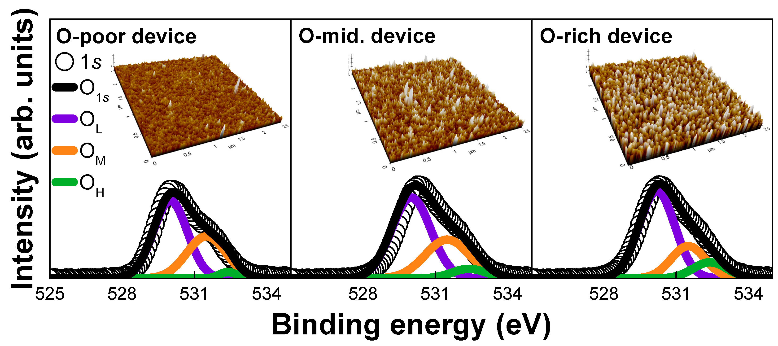
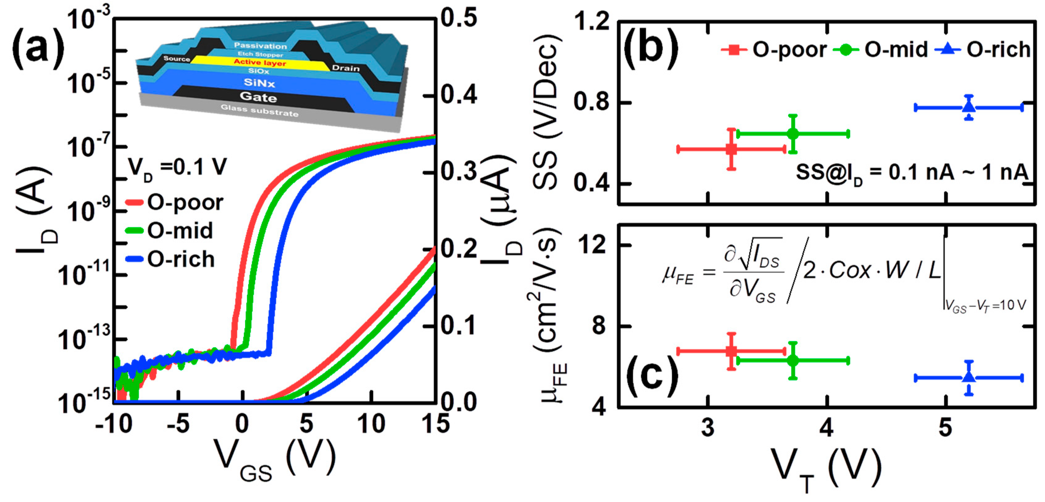
2. Experimental Procedure and Material Properties

The fabrication of a-IGZO TFTs with a bottom-gate structure is described as follows. The first room temperature (RT) sputtered deposition of a-IGZO on a glass substrate and patterning of the molybdenum (Mo) gate were followed by plasma-enhanced chemical vapor deposition (PECVD) of SiNX and SiO2 at 370 °C, which acted as a gate dielectric (the equivalent oxide thickness, Tox, was 258 nm). A 50 nm-thick a-IGZO thin film was then deposited by direct current (DC) sputtering (3 kW) at room temperature (RT) in a mixed atmosphere of Ar (35 sccm) and O2 by modulating the OFR to produce O-poor (21 sccm), O-mid (42 sccm), and O-rich (63 sccm) TFT devices. Next, an etch stopper (SiOX) layer was deposited by PECVD at 150 °C. For the formation of the source/drain (S/D) electrodes, Mo was sputtered at RT. A passivation layer (SiOX and SiNX; each 100 nm thick) was subsequently deposited. Finally, the devices were annealed at 250 °C for 1 h in a furnace. The width (Wch) and length of the device channel (Lch) were 200 and 100 μm, respectively.
To check if the OFR modulated the O-content in IGZO active films, the XPS spectra of the devices were analyzed. Figure 1 shows the O1s spectra of the IGZO films. The low-binding-energy component (OL) located at 530 eV is usually attributed to O2 ions surrounded by Zn, Ga, and in atoms in the IGZO compound system. The middle binding-energy component (OM) centered at 531.5 eV is associated with O2 ions that are in the oxygen-deficient regions of the IGZO matrix. Therefore, a change in the peak area ratio is related to the concentration of oxygen vacancies. OM-related oxygen vacancies supply free electron carriers in the IGZO film, resulting in an increase of electron concentration. The high binding-energy component (OH) located at 532.4 eV is mainly attributed to the presence of loosely bound, chemisorbed oxygen impurities (−CO3 adsorbed H2O or adsorbed O2) on the surface of the film. The observed O1s peak can be deconvoluted into three peaks, namely, OL, OM, and OH, as shown in Equation (1), and their characteristic parameters are summarized in Table 1:
O 1 s = O L + O M + O H = N L · exp ( ( E E L k T L ) 2 ) + N M · exp ( ( E E M k T M ) 2 ) + N H · exp ( ( E E H k T H ) 2 )
It is clearly observed in Figure 1 and Table 1 that OM decreases (from 33% to 28.5%) and OH increases (from 5% to 11%) as the OFR increases. The O-content is proportional to the OFR trend. The results of the XPS analysis suggest that the oxygen content in the IGZO film can be controlled by modulating the OFR during sputter deposition of the IGZO thin film. This is consistent with previous reports [6,7,8].
The surface roughness of the IGZO films was characterized by using atomic force microscopy (AFM, Suwon, Republic of Korea), the results of which are presented in the inset of Figure 1. The measured roughness values for O-poor, O-mid, and O-rich devices were 0.236, 0.386, and 0.562 nm, respectively. As the O-content becomes larger with increasing OFR, the IGZO surface becomes rougher.
The I–V characteristics of the IGZO TFTs were measured using an HP4156C (Keysight, Santa Rosa, CA, USA) semiconductor parameter analyzer at RT in the dark. The capacitance–voltage (C–V) characteristics were measured between the gate and the source tied to drain terminals by using an HP4294 LCR meter (Keysight, Santa Rosa, CA, USA). The subgap DOS was extracted using multi-frequency C–V spectroscopy [10], wherein frequencies of 2 kHz, 100 kHz, and 1 MHz were used with a ramp-up rate of 0.4 V/s and a small signal of 0.1 mV.
In terms of the VGS and VDS conditions under CS, three stress conditions were used during a stress time of 104 s: positive gate bias stress (PGBS), where VGS/VDS = 20/0 V; positive gate and drain bias stress (PGDBS), where VGS/VDS = 20/10 V regardless of the OFR; and target current stress (TCS) with 20 μA for various O-contents, where VGS/VDS = 20/10 V for O-poor, 20.5/11 V for O-mid, and 22/12 V for O-rich. PGBS and PGDBS were investigated first, after which the TCS was analyzed. Here, TCS means that the VGS/VDS condition varied depending on the O-content, where VGS is determined so that the value of overdrive voltage (VGS − VT) remains the same according to the O-content-dependent threshold voltage (VT). VDS is then determined such that the drain-to-source current (IDS) is maintained at the same value (20 μA) as that of the O-poor TFT at VGS/VDS = 20/10 V. Therefore, our TCS condition establishes both constant vertical electric field and constant current, at least in pristine states before CS.

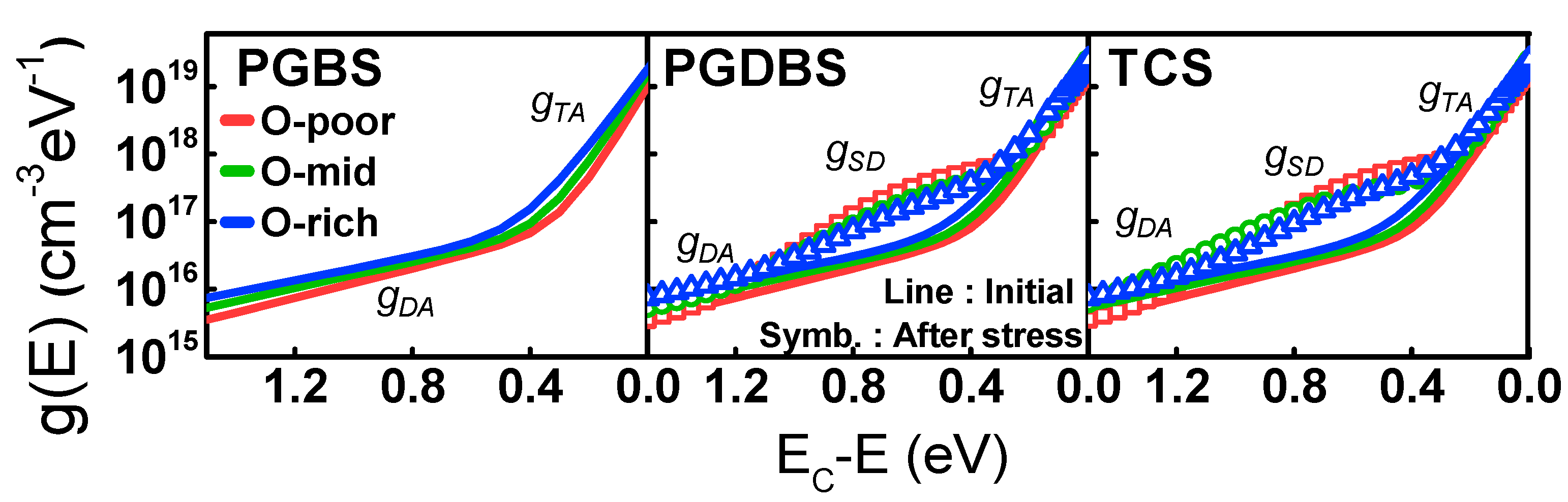
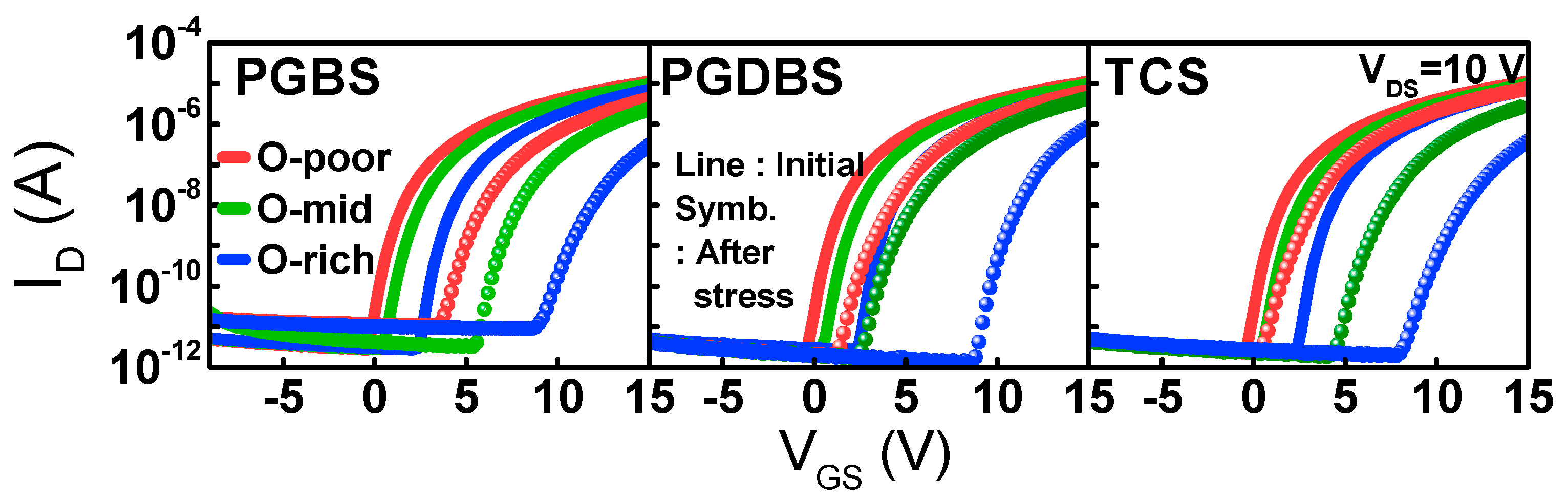
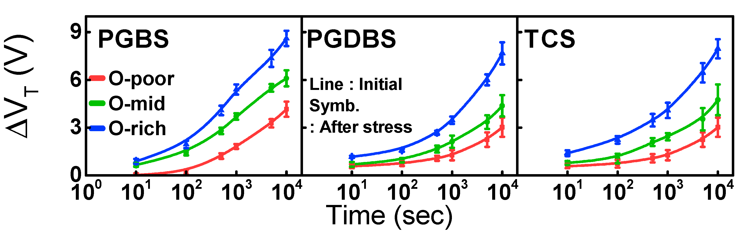
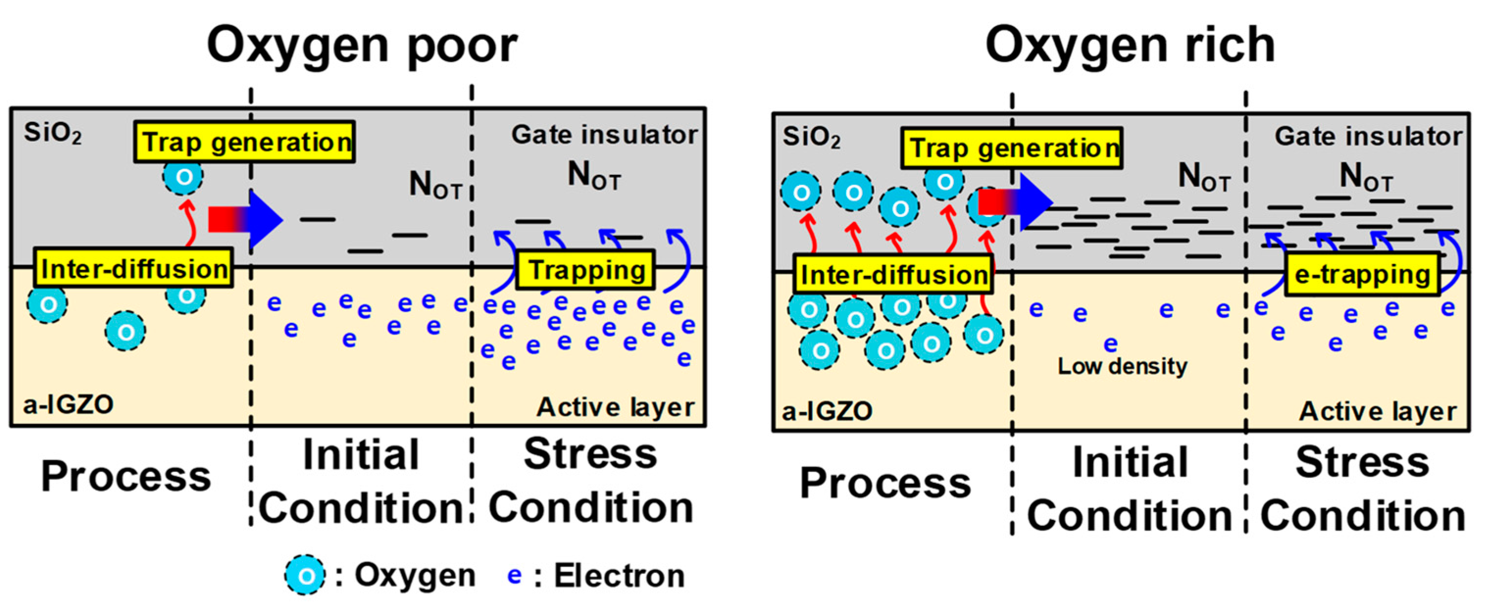
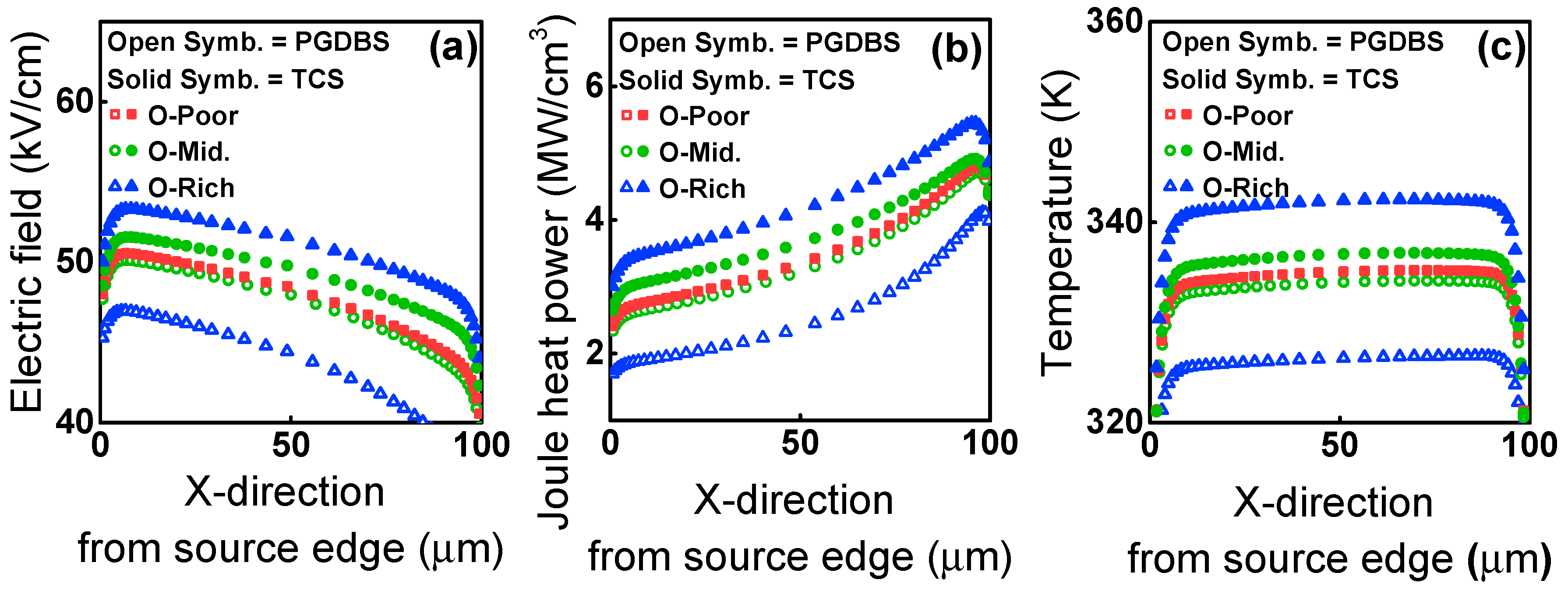
3. Results and Discussion

The O-content-dependent parameters of pristine TFT devices, such as I–V, VT, subthreshold swing (SS), and saturation field-effect mobility (μFE), are shown in Figure 2a–c, where VT was extracted by linear extrapolation. SS was determined from 10−10 to 10−9 A in the subthreshold region. In addition, μFE was extracted using the square root method at VGS − VT = 10 V and VDS = 10 V. With increasing OFR, i.e., with higher O-content, VT and SS increase, and μFE decreases, as shown Figure 2b,c. These results indicate that oxygen-related defects near the conduction band minimum (EC) increased with increasing OFR [11]. Therefore, the subgap DOS should be investigated to understand the effect of O-content on TFT performance and stability.
The extracted DOS (g(E)) values near the EC were divided into three components according to their energy level distribution: 1. shallow donor-like states, characteristic, and center energies of the Gaussian peaks (NSD, kTSD, and ESD), 2. acceptor-like deep states and characteristic NDA and kTDA, and 3. tail states and characteristic NTA and kTTA. The extracted g(E) value near EC was modeled according to Equation (2):
g ( E ) = g T A ( E ) + g D A ( E ) + g S D ( E ) = N T A exp ( E C E k T T A ) + N D A exp ( E C E k T D A ) + N S D exp ( ( E C E E S D k T S D ) 2 )
The extracted DOS and their parameters are summarized in Figure 3 and Table 2. They were extracted for the initial state and after PGBS, PGDBS, and TCS.
The effects of O-content on VT, SS, and μFE (Figure 2b,c) can be explained by considering both the XPS and AFM results (Figure 1) and the DOS (Figure 3). At first, VT increases as the O-content increases. This is explained by the decrease in the number of oxygen vacancies (VOs) in the TFT devices with larger O-content, as shown in the XPS spectra in Figure 1. VOs are well-known shallow donors [12,13]. Second, SS increases with increasing O-content, which is explained by the higher gTA(E) and gDA(E) in the TFT devices with more O-content, as shown in Figure 3. Higher gTA(E) and gDA(E) result from an ion bombardment process during the sputter deposition with the increase of OFR [11]. Finally, μFE decreases as the O-content increased, which can be explained as follows. In amorphous multi-metal oxides, some potential barriers are inherently present between neighboring ions at the EC and affect the electrons. Such barriers hinder electron transport and lower the mobility because of the different metal ion radii that result from the non-uniform overlap of conduction electron orbitals among In–O, Ga–O, and Zn–O bonds [14]. Subsequently, the percolation barrier height is effectively lowered because of the higher Fermi energy (EF) in lower O-content or higher VGS conditions, thus leading to higher μFE. Moreover, the AFM topography of the sample shown in Figure 1 suggests that either the surface roughness scattering or trap density in IGZO increases for higher O-content, which is another reason for lower μFE.
It is usually reported that the electrical performance in IGZO TFTs is significantly affected by trap sites near the EC [11]. Several key parameters such as surface roughness, gTA(E), gSD(E), and gDA(E) around the EC are both energetically and locally distributed throughout the energy bandgap with energy level dependency, causing carrier trapping and emission in each energy state (i.e., surface roughness scattering, multiple trapping, subgap hopping process, and thermal release events). Therefore, high trap density and high surface roughness decrease the mean free path of carriers and the ability to accumulate carriers, thus leading to the degradation of μFE and SS.
The IDS–VGS transfer characteristics before and after stress are shown in Figure 4. The CS-induced VT shift (ΔVT), which increased with O-content irrespective of the type of stress, is summarized in Figure 5. To clarify the degradation that occurred only in the a-IGZO active layer, g(E) values before and after CS were also compared, as shown in Figure 3 and Table 2. Under the influence of PGBS and/or PGDBS, VT of the TFTs frequently shifted in the positive direction. The physical origin of PBTS instability has been classified largely by either electron trapping (e-trapping) into the gate insulator (GI) interface [15,16] or the change in defect states in the active region [17]. In the former case, e-trapping becomes more accelerated with increasing temperature and/or electric field [18] as well as high density of electron traps in the gate insulator bulk interface. In the latter case, donor creation followed by a negative ΔVT occurs, especially in short-channel TFTs [19,20], whereas oxygen–dimer bond breaking was very recently observed as the physical origin of positive ΔVT [21]. Furthermore, in comparison with PGBS, ΔVT under PGDBS and/or TCS is very complicated because of various combinations of VGS and VDS, and competition between e-trapping and donor creation has been reported [22].
Only under PGDBS and TCS, i.e., when IDS flowed through the channel, were shallow donor states consistently created below the EC, as shown in Figure 3 and Table 2. The physical origin of donor creation is still controversial. In this study, it seemed to be dominated by VO ionization [19] or by peroxide formation [23]. Under PGDBS or TCS, electrons gained enough energy from the lateral field and were able to break the weakest oxygen bond or generate holes. In the former case, VOs that are not filled by electrons are generated by structure relaxation and are doubly positively charged (VO2+) [22]. In the latter case, hole-intermediated peroxide generation occurs, i.e., O2− + O2− → O22− + 2e. In both cases, donor creation lowers VT when stress is applied. This is contradictory to the observed positive ΔVT. Therefore, the dominant mechanism behind the positive ΔVT compensates donor creation (origin of a negative ΔVT), thus leading to eventual positive ΔVT. It can be assumed that the positive ΔVT during stress originates from the e-trapping in the GI.
To validate our assumption, we examined the relationship between hysteresis and ΔVT, as shown in Figure 6a. The hysteresis effect is known to change VT when VGS is swept from negative to positive values and then the transfer curve is measured again while sweeping from positive to negative VGS. That is, after accumulated carriers are trapped in shallow or deep traps of the GI, the captured carriers cause a screening effect to the VGS. Therefore, the hysteresis voltage (VHys) is a good indicator of the quality of the GI as well as the GI/IGZO interface. Here, VHys is defined as the difference in VT between double VGS sweeps, i.e., the sweep from 20 to −20 V and that from −20 to 20 V as denoted in Figure 6a. Figure 6a indicates that the oxygen-content-dependent, PGBS-induced ΔVT is well correlated with the VHys depending on the O-content, which validates the assumption that the PGBS/PGDBS/TCS-induced instability is dominated by e-trapping in the GI and/or interface.
The effect of O-content on ΔVT and VHys can be explained as follows. As the O-content in the a-IGZO active layer increases, a larger number of oxygen atoms at the interface or in the active layer diffuse into the SiO2 of GI owing to the stronger Si–O affinity in comparison to that of Ga–O, Zn–O, or In–O (Si–O > Ga–O > Zn–O > In–O) [24] during fabrication. Increased oxygen interstitials generate electron traps in the GI [25], which is consistent with relatively poor GI quality (i.e., larger ΔVT) and hysteresis in O-rich devices, as shown Figure 7. Here, NOT symbolizes the spatial density of electron traps in the GI.
Given the O-content of the active layer, the positive ΔVT increased in the following order: PGDBS < TCS < PGBS, as shown in Figure 5. In the PGBS condition, only e-trapping in the GI occurred effectively, both in the source and drain regions. However, in the PGDBS and TCS conditions, e-trapping near the drain was significantly alleviated, owing to the release of the vertical electric field and creation of donor states. Therefore, the largest positive ΔVT occurred for PGBS conditions.
In addition, it should be noted that, for a given O-content, ΔVT under TCS is larger than that under PGDBS. This can be explained by the self-heating assisted e-trapping [26,27,28], vertical electric field, and bulk oxide trap. To analyze the Joule heating effect under stress conditions, the average power consumption was calculated by multiplying the drain current by VDS under stress conditions, as shown in Figure 6b. Joule heating under TCS was greater than that under PGDBS. Such Joule heating accumulated from self-heating in the active layer as the thermal conductivity of a-IGZO is quite low [29]. E-trapping can then be activated to a greater extent via thermionic field emission-assisted GI trapping. Under PGDBS, although the O-poor device generated more heat in the active layer than that in the O-mid and O-rich devices, the ΔVT of the O-rich device was the largest. These results indicate that e-trapping is dominated by the NOT rather than by the self-heating effect. Therefore, GI quality is the key factor for determining ΔVT under TCS, PGDBS, and PGBS conditions for various O-contents. Self-heating-assisted e-trapping also becomes more significant for devices with the same O-content as the CS dissipates more Joule heating and power.
To validate our discussion, a well-calibrated TCAD simulation was performed by incorporating the energy band structure, a DOS model depending on the O-content, trap-limited conduction, and a self-heating model into Silvaco ATLAS-2D [30]. The electric field, Joule heating power, and device temperature were simulated under different conditions, as shown in Figure 8a–c. As shown in Figure 8c, regardless of the O-content, self-heating was more significant in TCS than in PGDBS. Therefore, as shown in Figure 6b, the ΔVT in TCS is larger than that in PGDBS irrespective of O-content. Here, it should be noted that, in the O-poor device, the TCS condition is the same as the PGDBS condition. Eventually, the CS-induced instability is determined by the increasing NOT with O-content and the ΔVT-compensation by donor creation. Specifically, under TCS, the increasing self-heating with O-content becomes another key factor, although both the initial vertical electric field and initial IDS are the same, independent of the O-content.
Our results suggest that the effect of O-content on CS-induced instability can be explained consistently for all cases considered in this study, i.e., TCS, PGDBS, and PGBS conditions.

4. Conclusions

The effect of O-content on CS-induced instability is investigated in bottom-gate a-IGZO TFTs. Under PGDBS and TCS conditions, donor creation was clearly observed in a-IGZO active regions. The observed positive ΔVT was dominated by e-trapping in the GI. Because the O-content affects the GI quality as well as the typical DC-performance parameters, such as VT, SS, and μFE, stress-induced ΔVT increased with increasing O-content irrespective of the type of stress. For specific O-content, ΔVT increased in the following order: PGDBS < TCS < PGBS, which can be explained by considering a combination of electric field relaxation via donor creation and self-heating-assisted e-trapping. Our results suggest that careful joint optimization of the GI and active layer is indispensable for designing highly stable a-IGZO TFTs. The detailed findings are useful for designing stable current-driving schemes for compensating electrical degradation and for circuits in high-frame-rate displays.

Author Contributions

S.C. and J.-Y.K. contributed equally to this work. Conceptualization, J.-Y.K., S.C. and D.H.K.; Formal analysis, J.-Y.K., S.C. and H.K.; Investigation, D.K. and J.R.; Methodology, J.-Y.K. and S.C.; Writing – original draft, J.-Y.K., S.C. and D.H.K.; Writing – review and editing, S.-J.C., D.M.K. and D.H.K.

Funding

This work was supported in part of National Research Foundation of Korea (NRF) through the Korean Government, Ministry of Education, Science and Technology (MEST), under Grant 2016R1A5A1012966, Grant 2017R1A2B4006982, Grant 18ZB1800, and Grant 2016M3A7B4909668.

Acknowledgments

The CAD software was supported by SILVACO and IDEC.

Conflicts of Interest

The authors declare no conflict of interest.

References

  1. Tani, R.; Yoon, J.; Yun, S.-I.; Nam, W.; Takasugi, S.; Kim, J.-M.; Park, J.; Kwon, S.; Kim, P.; Oh, C.; et al. 64.2: Panel and Circuit Designs for the World’s First 65-inch UHD OLED TV. SID Symp. Dig. Tech. Pap. 2015, 46, 950–953. [Google Scholar] [CrossRef]
  2. Kim, J.; Bang, S.; Lee, S.; Shin, S.; Park, J.; Seo, H.; Jeon, H. A study on H 2 plasma treatment effect on a-IGZO thin film transistor. J. Mater. Res. 2012, 27, 2318–2325. [Google Scholar] [CrossRef]
  3. Chen, W.-T.; Lo, S.-Y.; Kao, S.-C.; Zan, H.-W.; Tsai, C.-C.; Lin, J.-H.; Fang, C.-H.; Lee, C.-C. Oxygen-Dependent Instability and Annealing/Passivation Effects in Amorphous In-Ga-Zn-O Thin-Film Transistors. IEEE Electron. Dev. Lett. 2011, 32, 1552–1554. [Google Scholar] [CrossRef]
  4. Kim, K.A.; Park, M.J.; Lee, W.H.; Yoon, S.M. Characterization of negative bias-illumination-stress stability for transparent top-gate In-Ga-Zn-O thin-film transistors with variations in the incorporated oxygen content. J. Appl. Phys. 2015, 118. [Google Scholar] [CrossRef]
  5. Nomura, K.; Kamiya, T.; Hosono, H. Effects of diffusion of hydrogen and oxygen on electrical properties of amorphous oxide semiconductor, In-Ga-Zn-O. ECS J. Solid State Sci. Technol. 2012, 2, P5–P8. [Google Scholar] [CrossRef]
  6. Moon, Y.-K.; Lee, S.; Kim, D.-H.; Lee, D.-H.; Jeong, C.-O.; Park, J.-W. Application of DC magnetron sputtering to deposition of ingazno films for thin film transistor devices. Jpn. J. Appl. Phys. 2009, 48, 031301. [Google Scholar] [CrossRef]
  7. Nomura, K.; Takagi, A.; Kamiya, T.; Ohta, H.; Hirano, M.; Hosono, H. Amorphous oxide semiconductors for high-performance flexible thin-film transistors. Jpn. J. Appl. Phys. 2006, 45, 4303–4308. [Google Scholar] [CrossRef]
  8. Zhan, R.; Dong, C.; Liu, P.-T.; Shieh, H.-P.D. Influence of channel layer and passivation layer on the stability of amorphous In-Ga-Zn-O thin film transistors. Microelectron. Reliab. 2013, 53, 1879–1885. [Google Scholar] [CrossRef]
  9. Mtangi, W.; Auret, F.D.; Meyer, W.E.; Legodi, M.J.; Janse van Rensburg, P.J.; Coelho, S.M.M.; Diale, M.; Nel, J.M. Effects of hydrogen, oxygen, and argon annealing on the electrical properties of ZnO and ZnO devices studied by current-voltage, deep level transient spectroscopy, and Laplace DLTS. J. Appl. Phys. 2012, 111, 094504. [Google Scholar] [CrossRef] [Green Version]
  10. Lee, S.; Park, S.; Kim, S.; Jeon, Y.; Jeon, K.; Park, J.-H.; Park, J.; Song, I.; Kim, C.-J.; Park, Y.; et al. Extraction of subgap density of states in amorphous InGaZnO thin-film transistors by using multifrequency capacitanc-voltage characteristics. Electron. Device Lett. 2010, 31, 231–233. [Google Scholar]
  11. Kim, S.; Jeon, Y.W.; Kim, Y.; Kong, D.; Jung, H.K.; Bae, M.-K.; Lee, J.-H.; Du Ahn, B.; Park, S.Y.; Park, J.-H.; et al. Impact of oxygen flow rate on the instability under positive bias stresses in dc-sputtered amorphous In-Ga-Zn-O thin-film transistors. IEEE Electron. Device Lett. 2012, 33, 62–64. [Google Scholar] [CrossRef]
  12. Kamiya, T.; Nomura, K.; Hirano, M.; Hosono, H. Electronic structure of oxygen deficient amorphous oxide semiconductor a-InGaZnO 4-x: Optical analyses and first-principle calculations. Phys. Stat. Solidi 2008, 5, 3098–3100. [Google Scholar]
  13. Janotti, A.; Van de Walle, C.G. Oxygen vacancies in ZnO. Appl. Phys. Lett. 2005, 87, 122102. [Google Scholar] [CrossRef]
  14. Nomura, K.; Ohta, H.; Takagi, A.; Kamiya, T.; Hirano, M.; Hosono, H. Room-temperature fabrication of transparent flexible thin-film transistors using amorphous oxide semiconductors. Nature 2004, 432, 488–492. [Google Scholar] [CrossRef] [PubMed]
  15. Lee, J.-M.; Cho, I.-T.; Lee, J.-H.; Kwon, H.-I. Bias-stress-induced stretched-exponential time dependence of threshold voltage shift in InGaZnO thin film transistors. Appl. Phys. Lett. 2008, 93, 2–5. [Google Scholar] [CrossRef]
  16. Suresh, A.; Muth, J.F. Bias stress stability of indium gallium zinc oxide channel based transparent thin film transistors. Appl. Phys. Lett. 2008, 92, 033502. [Google Scholar] [CrossRef] [Green Version]
  17. Um, J.G.; Mativenga, M.; Migliorato, P.; Jang, J. Defect generation in amorphous-indium-gallium-zinc-oxide thin-film transistors by positive bias stress at elevated temperature. J. Appl. Phys. 2014, 115, 134502. [Google Scholar] [CrossRef]
  18. Mativenga, M.; Hong, S.; Jang, J. High current stress effects in amorphous-In-Ga-Zn-O4 thin-film transistors. Appl. Phys. Lett. 2013, 102, 1–4. [Google Scholar] [CrossRef]
  19. Kim, J.I.; Jeong, C.-Y.; Kwon, H.-I.; Jung, K.D.; Park, M.S.; Kim, K.H.; Seo, M.S.; Lee, J.-H. Modeling of asymmetric degradation based on a non-uniform electric field and temperature in amorphous In-Ga-Zn-O thin film transistors. Semicond. Sci. Technol. 2017, 32, 035017. [Google Scholar] [CrossRef]
  20. Lee, D.; Jeong, C.-Y.; Song, S.-H.; Xiao-Shi, J.; Kim, J.I.; Lee, J.-H.; Kwon, H.-I. Asymmetrical degradation behaviors in amorphous In-Ga-Zn-O thin-film transistors under various gate and drain bias stresses. J. Vac. Sci. Technol. B Nanotechnol. Microelectron. Mater. Process. Meas. Phenom. 2015, 33, 011202. [Google Scholar]
  21. Choi, S.; Jang, J.; Kang, H.; Baeck, J.H.; Bae, J.U.; Park, K.-S.; Yoon, S.Y.; Kang, I.B.; Kim, D.M.; Choi, S.-J.; et al. Systematic decomposition of the positive bias stress instability in self-aligned coplanar In-Ga-Zn-O thin-film transistors. IEEE Electron. Dev. Lett. 2017, 38, 580–583. [Google Scholar] [CrossRef]
  22. Choi, S.; Kim, H.; Jo, C.; Kim, H.-S.; Choi, S.-J.; Kim, D.M.; Park, J.; Kim, D.H. The effect of gate and drain fields on the competition between donor-like state creation and local electron trapping in In–Ga–Zn–O thin film transistors under current stress. IEEE Electron. Device Lett. 2015, 36, 1336–1339. [Google Scholar] [CrossRef]
  23. Nahm, H.-H.; Kim, Y.-S.; Kim, D.H. Instability of amorphous oxide semiconductors via carrier-mediated structural transition between disorder and peroxide state. Phys. Stat. Solidi 2012, 249, 1277–1281. [Google Scholar] [CrossRef]
  24. Oh, S.; Baeck, J.H.; Bae, J.U.; Park, K.-S.; Kang, I.B. Effect of interfacial excess oxygen on positive-bias temperature stress instability of self-aligned coplanar In-Ga-Zn-O thin-film transistors. Appl. Phys. Lett. 2016, 108, 141604. [Google Scholar] [CrossRef]
  25. Li, F.; Nathan, A. CCD Image Sensors in Deep-Ultraviolet; Microtechnology and Mems; Springer: Berlin/Heidelberg, Germany, 2005; ISBN 3-540-22680-X. [Google Scholar]
  26. Chen, T.-C.; Chang, T.-C.; Hsieh, T.-Y.; Tsai, M.-Y.; Chen, Y.-T.; Chung, Y.-C.; Ting, H.-C.; Chen, C.-Y. Self-heating enhanced charge trapping effect for In-Ga-Zn-O thin film transistor. Appl. Phys. Lett. 2012, 101, 042101. [Google Scholar] [CrossRef]
  27. Kim, J.I.; Chang, K.S.; Kim, D.U.; Cho, I.-T.; Jeong, C.-Y.; Lee, D.; Kwon, H.-I.; Jin, S.H.; Lee, J.-H. Thermoreflectance microscopy analysis on self-heating effect of short-channel amorphous In-Ga-Zn-O thin film transistors. Appl. Phys. Lett. 2014, 105, 043501. [Google Scholar] [CrossRef]
  28. Urakawa, S.; Tomai, S.; Ueoka, Y.; Yamazaki, H.; Kasami, M.; Yano, K.; Wang, D.; Furuta, M.; Horita, M.; Ishikawa, Y.; et al. Thermal analysis of amorphous oxide thin-film transistor degraded by combination of joule heating and hot carrier effect. Appl. Phys. Lett. 2013, 102, 2011–2015. [Google Scholar] [CrossRef]
  29. Yoshikawa, T.; Yagi, T.; Oka, N.; Jia, J.; Yamashita, Y.; Hattori, K.; Seino, Y.; Taketoshi, N.; Baba, T.; Shigesato, Y. Thermal Conductivity of amorphous Indium-Gallium-Zinc Oxide thin films. Appl. Phys. Express 2013, 6, 021101. [Google Scholar] [CrossRef]
  30. ATLAS User’s Manual; Silvaco: Santa Clara, CA, USA, 2018.
Figure 1. X-ray photoelectron spectroscopy (XPS) O1s spectra of InGaZnO (IGZO) films upon varying the flow rate in a mixed atmosphere of Ar and O2 (oxygen flow rate (OFR) = 35 sccm). The OFR is modulated to produce O-poor (OFR = 21 sccm), O-mid (42 sccm), and O-rich (63 sccm) IGZO thin films. The inset shows the surface morphology of IGZO thin films as a function of OFR, as observed by atomic force microscopy (AFM).
Materials 12 03149 g001
Figure 2. (a) IDVGS transfer curve characteristic at VDS = 0.1 V for various O-contents. The inset is the fabricated a-IGZO thin-film transistor (TFT) with an inverted staggered bottom-gate structure. The statistical data of (b) subthreshold swing (SS)-VT, and (c) μFE-VT were extracted from 10 devices for each O-content.
Materials 12 03149 g002
Figure 3. Density of states (DOS) over a range of O-content as stress time under positive gate bias stress (PGBS), positive gate and drain bias stress (PGDBS), and target current stress (TCS). Lines denote the initial state, and symbols indicate values after each stress condition.
Materials 12 03149 g003
Figure 4. Transfer VGS–IDS characteristics at VDS = 10 (V) over a range of O-content as stress time under PGBS, PGDBS, and TCS. Lines denote the initial state, and symbols indicate values after each stress condition.
Materials 12 03149 g004
Figure 5. ΔVT for various O-contents as stress time under PGBS, PGDBS, and TCS.
Materials 12 03149 g005
Figure 6. The OFR-dependent relationships (a) between ΔVT and VHys and (b) between ΔVT and the average power consumption under PGDBS and TCS. Closed symbols denote PGDBS conditions, and open symbols indicate TCS conditions.
Materials 12 03149 g006
Figure 7. Production of electron trap centers according to O-content.
Materials 12 03149 g007
Figure 8. The simulated (a) electric field, (b) Joule heat power, and (c) temperature of the device based on the configuration of VGS/VDS.
Materials 12 03149 g008
Table 1. Extracted XPS parameters (initial).
O-ContentO-PoorO-MediumO-Rich
OLNL (A.U)1.20 × 1051.25 × 1051.30 × 105
KTL (eV)1
EL (eV)530
OMNM (A.U.)0.65 × 1050.60 × 1050.50 × 105
KTM (eV)1.151.11.1
EM (eV)531.5
OHNH (A.U.)0.10 × 1050.2 × 1050.25 × 105
KTH (eV)0.50.751
EH (eV)532.4
Table 2. Extracted DOS parameters (initial and after PGBS, PGDBS, and TCS).
Parameter O-ContentStress ConditionNdos
(eV−1 cm−3)
kTdos
(eV)
Edos
(eV)
gTA (E)O-poorAll conditions2.0 × 10190.06
O-midAll conditions2.3 × 10190.065
O-richAll conditions3.0 × 10190.075
gDA (E)O-poorAll conditions1.5 × 10170.4
O-midAll conditions1.6 × 10170.47
O-richAll conditions1.9 × 10170.5
gSD (E)O-poorInitial0.4–0.450.3
After PGBS
After PGDBS5 × 1017
After TCS6 × 1017
O-midInitial
After PGBS
After PGDBS3 × 1017
After TCS3 × 1017
O-richInitial
After PGBS
After PGDBS2 × 1017
After TCS3 × 1017

