High-Mobility Inkjet-Printed Indium-Gallium-Zinc-Oxide Thin-Film Transistors Using Sr-Doped Al2O3 Gate Dielectric

Abstract
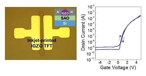
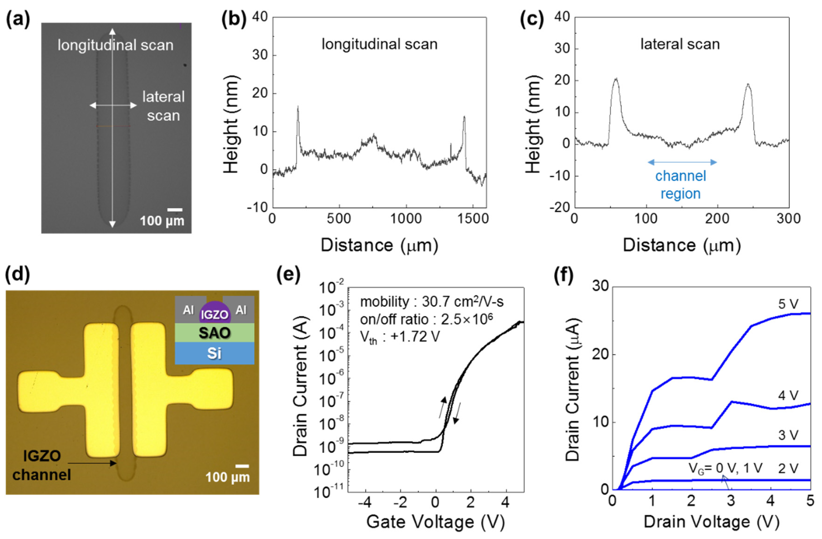
:
1. Introduction
2. Experimental Procedure
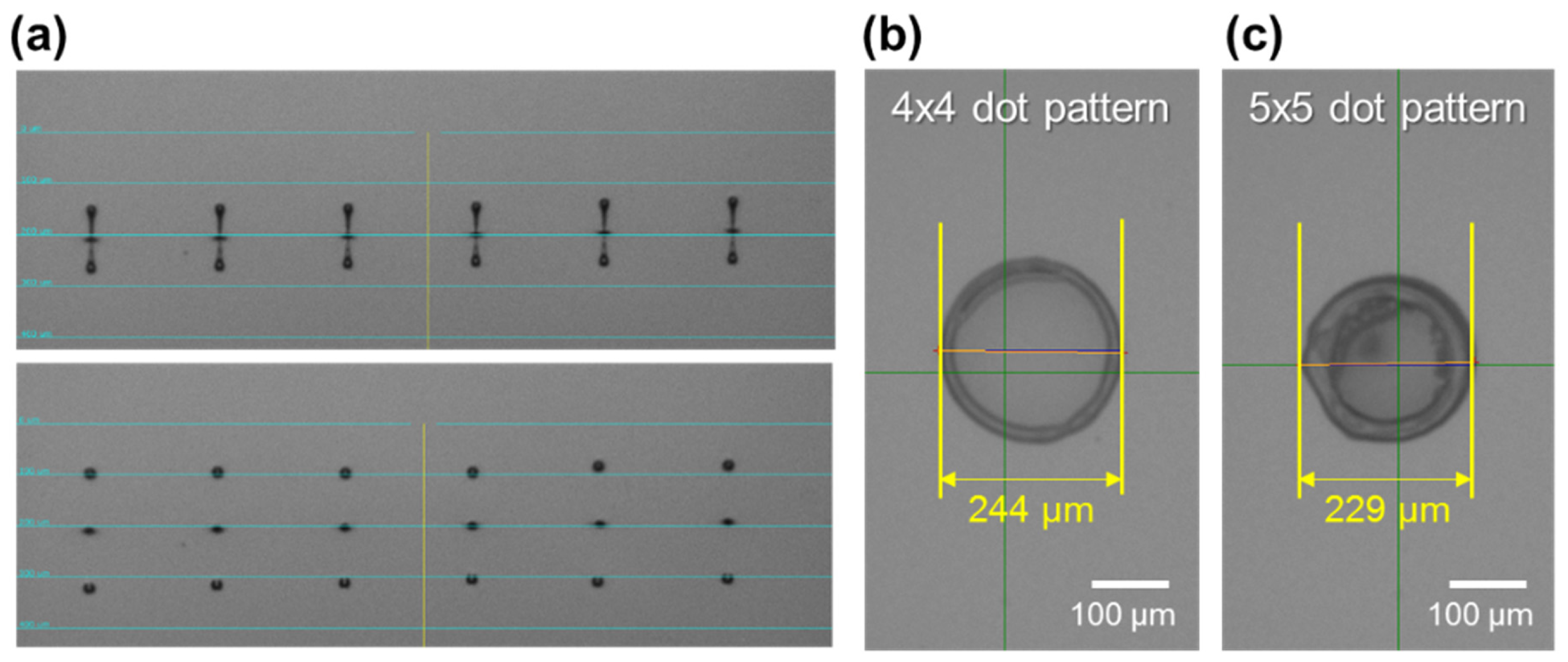
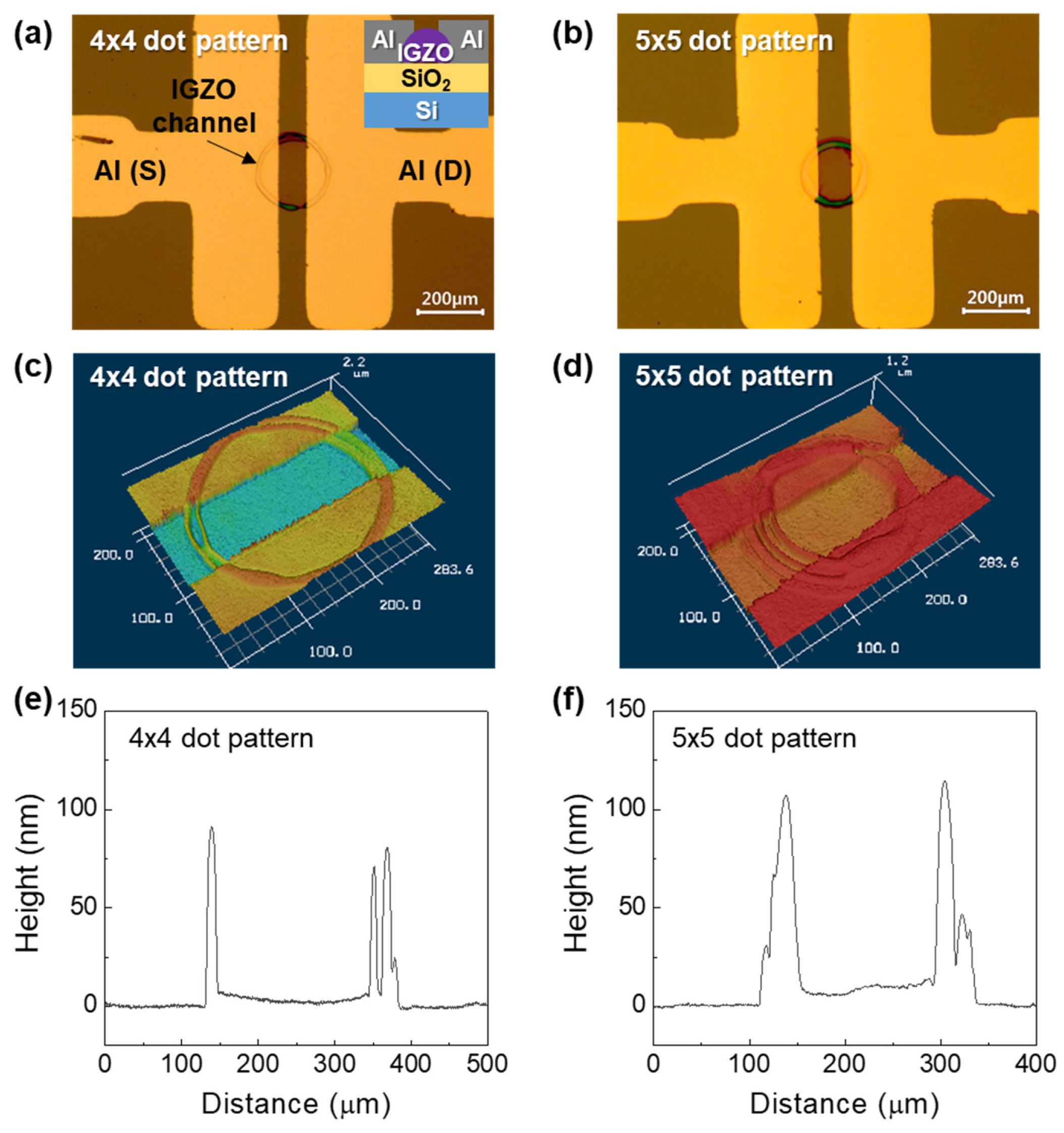
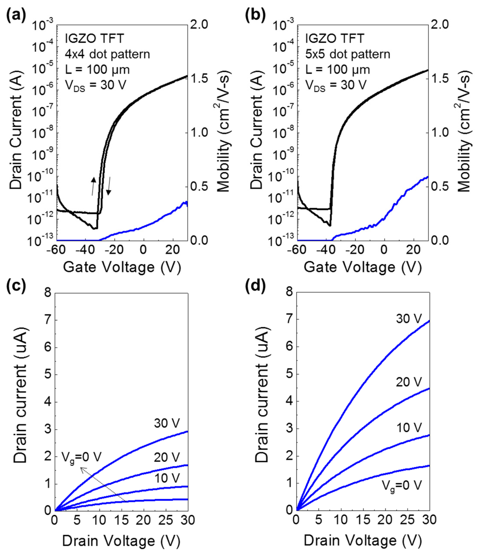
3. Results and Discussion
4. Conclusions
Author Contributions
Funding
Conflicts of Interest
References
- Nomura, K.; Ohta, H.; Takagi, A.; Kamiya, T.; Hirano, M.; Hosono, H. Room-temperature fabrication of transparent flexible thin-film transistors using amorphous oxide semiconductors. Nature 2004, 432, 488–492. [Google Scholar] [CrossRef] [PubMed]
- Oh, M.S.; Lee, K.; Lee, K.H.; Cha, S.H.; Choi, J.M.; Lee, B.H.; Sung, M.M.; Im, S. Transparent photo-stable complementary inverter with an organic/inorganic nanohybrid dielectric layer. Adv. Funct. Mater. 2009, 19, 726–732. [Google Scholar] [CrossRef]
- Banger, K.K.; Yamashita, Y.; Mori, K.; Peterson, R.L.; Leedham, T.; Rickard, J.; Sirringhaus, H. Low-temperature, high-performance solution-processed metal oxide thin-film transistors formed by a “sol–gel on chip” process. Nat. Mater. 2011, 10, 45–50. [Google Scholar] [CrossRef]
- Fortunato, E.; Barquinha, P.; Martins, R. Oxide semiconductor thin-film transistors: A review of recent advances. Adv. Mater. 2012, 24, 2945–2986. [Google Scholar] [CrossRef]
- Fernandes, C.; Santa, A.; Santos, Â.; Bahubalindruni, P.; Deuermeier, J.; Martins, R.; Fortunato, E.; Barquinha, P. A sustainable approach to flexible electronics with zinc-tin oxide thin-film transistors. Adv. Electron. Mater. 2018, 4, 1800032. [Google Scholar] [CrossRef]
- Kim, M.-G.; Kanatzidis, M.G.; Facchetti, A.; Marks, T.J. Low-temperature fabrication of high-performance metal oxide thin-film electronics via combustion processing. Nat. Mater. 2011, 10, 382–388. [Google Scholar] [CrossRef] [PubMed]
- Hwang, Y.H.; Seo, J.; Yun, J.M.; Park, H.; Yang, S.; Ko Park, S.; Bae, B. An ‘aqueous route’ for the fabrication of low-temperature-processable oxide flexible transparent thin-film transistors on plastic substrates. NPG Asia Mater. 2013, 5, e45. [Google Scholar] [CrossRef]
- Jun, T.; Song, K.; Jeong, Y.; Woo, K.; Kim, D.; Bae, C.; Moon, J. High-performance low-temperature solution-processable ZnO thin film transistors by microwave-assisted annealing. J. Mater. Chem. 2011, 21, 1102–1108. [Google Scholar] [CrossRef]
- Kim, Y.-H.; Heo, J.-S.; Kim, T.-H.; Park, S.; Yoon, M.-H.; Kim, J.; Oh, M.S.; Yi, G.-R.; Noh, Y.-Y.; Park, S.K. Flexible metal-oxide devices made by room-temperature photochemical activation of sol-gel films. Nature 2012, 489, 128–132. [Google Scholar] [CrossRef] [PubMed]
- Park, S.K.; Kim, Y.-H.; Han, J.-I. All solution-processed high-resolution bottom-contact transparent metal-oxide thin film transistors. J. Phys. D. Appl. Phys. 2009, 42, 125102. [Google Scholar] [CrossRef]
- Lee, W.J.; Park, W.T.; Park, S.; Sung, S.; Noh, Y.Y.; Yoon, M.H. Large-scale precise printing of ultrathin sol-gel oxide dielectrics for directly patterned solution-processed metal oxide transistor arrays. Adv. Mater. 2015, 27, 5043–5048. [Google Scholar] [CrossRef]
- Sung, S.; Park, S.; Cha, S.; Lee, W.J.; Kim, C.H.; Yoon, M.H. Direct patterning of sol-gel metal oxide semiconductor and dielectric films via selective surface wetting. RSC Adv. 2015, 5, 38125–38129. [Google Scholar] [CrossRef]
- Jang, J.; Kang, H.; Chakravarthula, H.C.; Subramanian, V. Fully inkjet-printed transparent oxide thin film transistors using a fugitive wettability switch. Adv. Electron. Mater. 2015, 1, 1500086. [Google Scholar] [CrossRef]
- Zhang, Q.; Shao, S.; Chen, Z.; Pecunia, V.; Xia, K.; Zhao, J.; Cui, Z. High-resolution inkjet-printed oxide thin-film transistors with a self-aligned fine channel bank structure. ACS Appl. Mater. Interfaces 2018, 10, 15847–15854. [Google Scholar] [CrossRef]
- Li, Y.; Lan, L.; Gao, P.; He, P.; Dai, X.; Cao, H.; Liang, L.; Peng, J. Inkjet-printed Self-aligned short-channel metal-oxide thin-film transistors based on coffee stripe dewetting method. IEEE Electron. Device Lett. 2019, 40, 228–231. [Google Scholar] [CrossRef]
- Li, Y.; Lan, L.; Sun, S.; Lin, Z.; Gao, P.; Song, W.; Song, E.; Zhang, P.; Peng, J. All inkjet-printed metal-oxide thin-film transistor array with good stability and uniformity using surface-energy patterns. ACS Appl. Mater. Interfaces 2017, 9, 8194–8200. [Google Scholar] [CrossRef]
- Chung, S.; Cho, K.; Lee, T. Recent progress in inkjet-printed thin-film transistors. Adv. Sci. 2019, 1801445. [Google Scholar] [CrossRef]
- Deegan, R.D.; Bakajin, O.; Dupont, T.F.; Huber, G.; Nagel, S.R.; Witten, T.A. Capillary flow as the cause of ring stains from dried liquid drops. Nature 1997, 389, 827–829. [Google Scholar] [CrossRef]
- Yang, W.; Song, K.; Jung, Y.; Jeong, S.; Moon, J. Solution-deposited Zr-doped AlOx gate dielectrics enabling high-performance flexible transparent thin film transistors. J. Mater. Chem. C 2013, 1, 4275–4282. [Google Scholar] [CrossRef]
- Kim, J.; Choi, S.; Jo, J.W.; Park, S.K.; Kim, Y.H. Solution-processed lanthanum-doped Al2O3 gate dielectrics for high-mobility metal-oxide thin-film transistors. Thin Solid Films 2018, 660, 814–818. [Google Scholar] [CrossRef]
- Kim, J.; Choi, S.; Kim, M.; Ha, T.J.; Kim, Y.-H. Strontium doping effects on the characteristics of solution-processed aluminum oxide dielectric layer and its application to low-voltage-operated indium-gallium-zinc-oxide thin-film transistors. Ceram. Int. 2017, 43, 13576–13580. [Google Scholar] [CrossRef]
- Kalb, W.L.; Batlogg, B. Calculating the trap density of states in organic field-effect transistors from experiment: A comparison of different methods. Phys. Rev. B 2010, 81, 035327. [Google Scholar] [CrossRef]


© 2019 by the authors. Licensee MDPI, Basel, Switzerland. This article is an open access article distributed under the terms and conditions of the Creative Commons Attribution (CC BY) license (http://creativecommons.org/licenses/by/4.0/).
Share and Cite
Choi, S.; Kim, K.-T.; Park, S.K.; Kim, Y.-H. High-Mobility Inkjet-Printed Indium-Gallium-Zinc-Oxide Thin-Film Transistors Using Sr-Doped Al2O3 Gate Dielectric. Materials 2019, 12, 852. https://doi.org/10.3390/ma12060852
Choi S, Kim K-T, Park SK, Kim Y-H. High-Mobility Inkjet-Printed Indium-Gallium-Zinc-Oxide Thin-Film Transistors Using Sr-Doped Al2O3 Gate Dielectric. Materials. 2019; 12(6):852. https://doi.org/10.3390/ma12060852
Chicago/Turabian StyleChoi, Seungbeom, Kyung-Tae Kim, Sung Kyu Park, and Yong-Hoon Kim. 2019. "High-Mobility Inkjet-Printed Indium-Gallium-Zinc-Oxide Thin-Film Transistors Using Sr-Doped Al2O3 Gate Dielectric" Materials 12, no. 6: 852. https://doi.org/10.3390/ma12060852
APA StyleChoi, S., Kim, K.-T., Park, S. K., & Kim, Y.-H. (2019). High-Mobility Inkjet-Printed Indium-Gallium-Zinc-Oxide Thin-Film Transistors Using Sr-Doped Al2O3 Gate Dielectric. Materials, 12(6), 852. https://doi.org/10.3390/ma12060852