Article

Study of Structural and Optoelectronic Properties of Thin Films Made of a Few Layered WS2 Flakes

by
Anna Łapińska
*,
Michał Kuźniewicz
,
Arkadiusz P. Gertych
,
Karolina Czerniak-Łosiewicz
,
Klaudia Żerańska-Chudek
,
Anna Wróblewska
,
Michał Świniarski
,
Anna Dużyńska
,
Jarosław Judek
and
Mariusz Zdrojek
Faculty of Physics, Warsaw University of Technology, Koszykowa 75, 00-662 Warsaw, Poland
*
Author to whom correspondence should be addressed.
Materials 2020, 13(23), 5315; https://doi.org/10.3390/ma13235315
Submission received: 21 October 2020 / Revised: 13 November 2020 / Accepted: 19 November 2020 / Published: 24 November 2020
(This article belongs to the Special Issue Novel Thin Films: Electrical and Optical Properties)

Abstract

:
We report a surfactant-free exfoliation method of WS2 flakes combined with a vacuum filtration method to fabricate thin (<50 nm) WS2 films, that can be transferred on any arbitrary substrate. Films are composed of thin (<4 nm) single flakes, forming a large size uniform film, verified by AFM and SEM. Using statistical phonons investigation, we demonstrate structural quality and uniformity of the film sample and we provide first-order temperature coefficient χ, which shows linear dependence over 300–450 K temperature range. Electrical measurements show film sheet resistance RS = 48 MΩ/□ and also reveal two energy band gaps related to the intrinsic architecture of the thin film. Finally, we show that optical transmission/absorption is rich above the bandgap exhibiting several excitonic resonances, and nearly feature-less below the bandgap.

1. Introduction

The group of 2D materials is wide and consists of materials with diverse properties. That diversity enables 2D materials to be used in various applications like nanoelectronics, energy storage, or photonics [1,2,3,4]. Transition Metals Dichalcogenides (TMDs) are an example of such 2D materials, including tungsten disulfide (WS2), the most studied representative of TMDs. WS2 is a semiconductor with a tuneable direct-indirect bandgap varying from 1.3 to 2.1 eV, for bulk form and monolayer, respectively [5,6]. The bulk form of WS2 is popular in the industry due to its lubricanting properties, whereas the 2D counterpart of WS2 is known for e.g., interesting electronic and optical properties [7], including a strong Kerr effect, third-order non-linear optical response, or giant two-photon absorption [8]. Its electron mobility has been reported in previous studies and equals 50 ± 7 cm2V−1s−1, ON/OFF ratio is usually around 106 [9,10,11,12]. Thus, WS2 is currently a material of great interest to the scientific world, as it is a very promising building block for future beyond-silicon optoelectronics. However, the mentioned properties of WS2 have been reported only for individual mono- and few layers fabricated via mechanical exfoliation or chemical vapour deposition. It would be particularly interesting to verify whether, and to what extent those properties can be inherited by more complex systems made of WS2 flakes—thin films. The first step to achieve this is to produce a large quantity of flakes and form thin films out of it. For this purpose, liquid-phase exfoliation (LPE) technique can be used. This technique can be modified in many ways and uses various solvents and equipment. Originally, ultrasonic agitation with N-methyl-2-pyrrolidone (NMP) had been utilised in the LPE method [13]. So far, a lot of different solvents had been used as a modification of LPE method for WS2 exfoliation, e.g., DMF (dimethyloformamide), aqueous PVA (polyvinyl alcohol), water and ethanol, acetone and isopropanol, isopropanol and water, SDS (sodium dodecyl sulfate), etc. [14,15,16,17,18,19,20].
Until now, the NMP has been the most frequently used solvent for the LPE method. It provides a high concentration of exfoliated flakes and a decent shelf-life, but on the other hand, it is an expensive and highly toxic diluent, limiting possible applications outside laboratories [21,22]. Hence, safer solvents are under consideration, e.g., mixture of DI (deionized) water and IPA (isopropyl alcohol) [18]. Flakes exfoliated using LPE techniques can be further employed in the vacuum filtration method to form different kinds of films [23,24,25,26].
Literature provides reports concerning thick free-standing films or heterostructures based on WS2 [13,23,24]. For instance, Lu et al. reports thin heterostructures made of graphene and WS2 films [24]. The work shows mostly nonlinear optical characteristics of relatively thin layered sandwiches with different thickness (from 60 to 135 nm). On the other hand, Coleman et al. [13,23] demonstrate the production of thick films (50 µm thick) made of WS2 and MoS2, and hybrid films (200 nm thick) made of WS2 and Single Walled Carbon Nanotubes (SWCNT). Reported samples show significant enhancement of over 500 times, compared to disordered WS2 films, of thermoelectric properties [25]. Up to now, there were no reports about stable, thin, and transferable WS2 films.
Here, we demonstrate how to fabricate very thin WS2 films using the liquid-phase exfoliation method without employing harsh chemical reagents and how to transfer it to any arbitrary substrate. The films are composed of thin single flakes (few nanometres thick), forming large size uniform layer, as verified by AFM and SEM. Statistical phonons investigation confirms structural quality and uniformity of the film sample. The temperature-dependent Raman study provides first-order temperature coefficient χ, which is linear over the whole studied temperature range. Moreover, we study the film sheet resistance and also temperature-dependent electrical properties revealing two energy bandgaps related to the intrinsic architecture of the thin film. Finally, we show that optical transmission/absorption above the bandgap exhibits several excitonic resonances, while it is nearly feature-less below the bandgap.

2. Materials and Methods

Si/SiO2 and microscope slides, cut in ~1 cm2 pieces were used as substrates in this work. The Si/SiO2 wafers were 500–550 µm thick, with silicon oxide thickness of 285 ± 30 nm and were N type antimony doped.
Atomic Force Microscopy (AFM, Brucker Icon, Billerica, MA, USA) has been used for structural characterization–topography, morphology, individual flakes, and film thickness. Electron microscopy (SEM, eLine Plus, GmbH, Dortmund, Germany) has been used for defining the continuity, purity, homogeneity of the fabricated thin film.
Raman study including individual, statistical measurements, and advance thermal characterization had been conducted using Renishaw inVia Raman Spectrometer, Wotton-under-Edge, Gloucestershire, UK. All Raman experiments had been performed in backscattering configuration, in ambient conditions, using green laser wavelength (λ = 532 nm) with low power density in order to avoid damaging the WS2 flakes and to prevent additional heating. Temperature-dependent measurement has been conducted in the 300–460 K range. Detailed parameters of each peak were extracted using the Lorentz curve fitting using Marquardt–Levenberg algorithm.
The electrical characterization was carried out using 4 probe measurements in van der Pauw configuration. The four palladium contacts were thermally evaporated on the sample using a mechanical mask technique. The four-probe measurements have been done using Keithley 2450 Source Measure Unit as a current source, Keithley 2182A nanovoltmeter and Keithley 7001 Switch System for proper system configuration control. The sample was placed in the cryostat MicrostatHe2 and Mercury intelligent temperature controller (iTC) system, Oxford, UK for temperature measurements in vacuum conditions (p~10−5 mbar). The temperature range from 330 K to 440 K was limited due to setup limitations. For proper evaluation of the 4 probe resistances for each contact configuration, we made an I–V characteristic to get the value of slope (resistance).
The Ultraviolet-Visible (UV-Vis) optical measurements (transmittance and reflectance) were made using a photovoltaic (PV) response analyser (PVE300 Bentham, Berkshire, UK) in the range of 300–1700 nm.

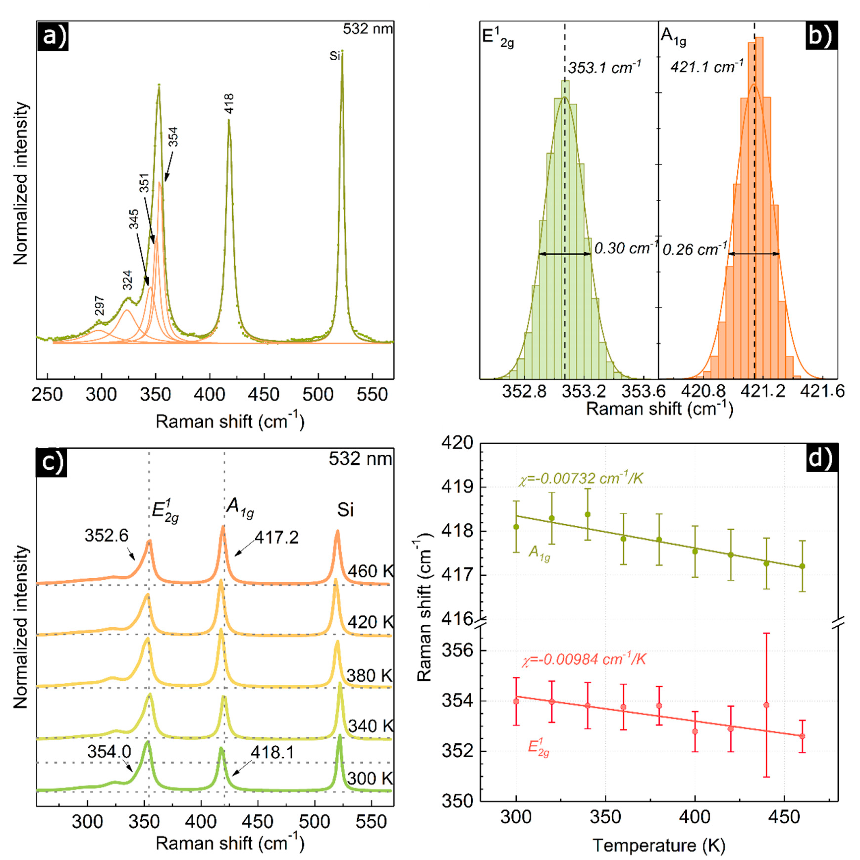
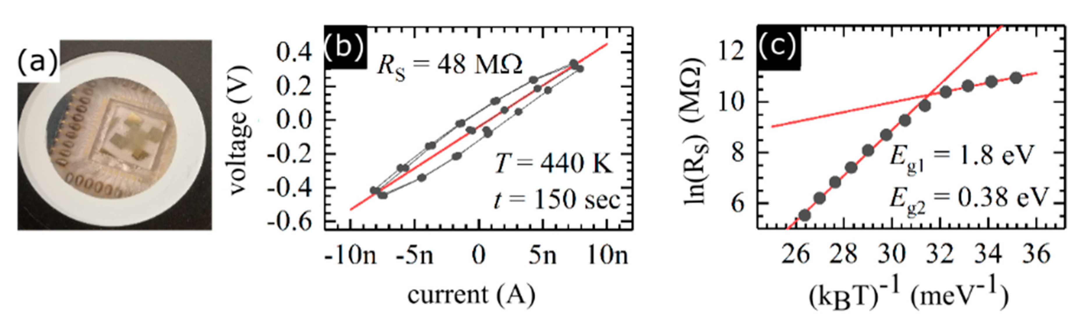
3. Results and Discussion

The starting point for thin WS2 films fabrication is the preparation of the bulk powder suspension and the exfoliation in liquid phase down to individual flakes. Suspensions containing WS2 were fabricated using non-harmful, relatively cheap solvents as DI water, and IPA. Commercially available bulk WS2 powder purchased from American Elements was used as a precursor in the exfoliation process. In the beginning, a ~0.1 g of 2D micropowder was added to the DI/IPA mixture, previously mixed in the ratio of 7:3. This ratio provides surface tension of approximate value of 40 mN/m, which is similar to NMP’s surface tension [26]. The prepared mixture was placed in an ultrasound bath at maximum power (320 W) for 3 h. After each hour, water in the sonication bath was changed to prevent overheating of the suspension. Then the suspension was centrifuged to remove unexfoliated 2D crystals at 2500 rpm for 75 min. The supernatant was collected and saved for thin-film fabrication. The example of prepared suspension is shown in Figure 1a.
Further, the thin WS2 films were produced directly from the exfoliated flakes suspension employing a vacuum filtration method which was conducted as explained below. A 15 mL of suspension was filtered through the cellulose (Millipore) filter with the pore sizes of 25 nm. After WS2 film formation on the filter, the setup had been left under vacuum for 2 h to dry off the film and next the vacuum was switched off and left overnight to complete the drying process. Next, the dry film was transferred from the filter to the substrate (any substrate could be used provided that it is resistant to the solvent used during transfer). Here, a Si/SiO2 (285 nm thickness of SiO2) and glass substrates have been used. The procedure of transferring film from cellulose filter is adapted and optimized from the commonly used method for Carbon Nanotubes (CNT) films [27]. In detail, the film on the filter was gently immersed into isopropyl alcohol and then cut to smaller pieces (5 mm × 5 mm). Each piece of the filter was placed film-side down against the desired substrate and immediately suspended over a bath of boiling acetone (heated to 75 °C) for two hours. This procedure allowed the gentle dissolution of the cellulose filter. Afterwards, the samples were immersed several times in a pure non-heated acetone bath to remove the residual filter from the samples. Finally, samples are placed into an isopropanol bath for a few minutes and then dried with compressed nitrogen.
We note that the above-described method of production of thin films using DI/IPA based suspension and the possibility to transfer films on different substrates is universal for other 2D materials such as GeS, GeSe, SnSe2, hBN, NbSe2, MoS2 [28], as shown in the Supplementary Information in Figures S4 and S5.
The image of thin-film and SEM scan of its surface are shown in Figure 1b,c, demonstrating the continuity of the film. Based on an AFM scan of individual flakes (see Supplementary Information, Figure S3) distribution of flake’s thickness was determined, which is provided in Figure 1d. The average flake thickness is estimated to ~3.9 (±1.5) nm. Accordingly, also to AFM, the roughness parameter of the whole film was estimated to be ~7 nm (Figure S1, Supporting Information) and the averaged thickness of the whole film was measured to be ~45 nm. The film thickness had been evaluated by measuring the AFM profile on the edge of the film (see Supplementary Information, Figure S2).
The structural properties of WS2 film were verified using Raman spectroscopy. Figure 2a presents a typical single Raman spectrum of WS2 thin film (on SiO2/Si substrate) exhibiting two main peaks: E12g (~353 cm−1) and A1g (~421 cm−1) accompanied by several lower energy peaks. The spectrum is consistent with other spectra obtained for WS2 flakes [29,30]. Statistical analysis of main phonon position distributions is further performed using the Raman mapping approach, where data is collected within 1 mm × 1 mm spatial map with step: 4 μm, delivering 251 × 251 single plots (see Figure 2b). Data presented in a form of histograms of peak position (phonon energy) clearly shows the structural uniformity of main Raman modes position distribution (full width at half maximum(FWHM) < 0.3 cm−1 in large areas of the WS2 film. The fluctuation of modes position is relatively low and mainly depends on the different thickness of the individual flakes distribution. In addition, the averaged difference between two main modes (A1g–E12g) is ~68 cm−1, suggesting that individual flakes thickness corresponds to several layers (~5–6) [31], which is also consistent with AFM study [32] (see Figure 1d).
Next, the temperature-dependent Raman analysis was performed. Figure 2c shows the evolution of Raman spectra with increasing temperature in the 300–460 K range. The main Raman modes E12g and A1g downshift with increasing temperature by 1.39 and 0.9 cm−1 respectively, which is an expected behaviour for any type of 2D materials [33,34,35]. To quantify the described effect, one can derive first-order temperature coefficient according to the following equation: ω ( T ) = ω 0 + χ T , where: χ—is the first order temperature coefficient, ω 0 —phonon frequency at 0 K. Based on this equation the extracted χ coefficient values: 0.00732 cm−1/K for mode E12g and 0.00984 cm−1/K for mode A1g. Interestingly, these values are approximately up to two times lower than for supported and suspended single WS2 crystals made by chemical vapor deposition (CVD) [6]. The lower value of χ likely stems from a large number of interfaces between flakes within the film that could significantly lower the thermal dissipation properties of the whole film. The values of χ for WS2 film could be useful for the determination of the thermal conductivity of the thin film [6].
The electrical measurements have been performed using the 4 probe method (see Figure 3a showing the device used in our study), which ensures that there is no contribution of contacts and wiring resistance on the sample’s sheet resistance (RS). Measurements took place in the temperature range of 300 K–440 K. Figure 3b illustrates current-voltage (I-V) characteristics in a form of hysteresis proving that measurements are repeatable. The origin of the hysteresis stem from a large number of interfaces between flakes in the film and film-metal contact interface that could lead to some charging effects. We found that the resistance of WS2 thin film is relatively high (RS = 48 MΩ/□ for T = 440 K), but not significantly different than previously reported [36]. Figure 3c shows the natural logarithm of the RS versus (kBT)−1, where the slope of the linear dependence directly represents the value of the activation energy. One can see that we have obtained two linear regions, which are represented by two activation energies of Eg1 = 1.8 eV, and Eg2 = 0.38 eV. This suggests that electronic transport in such disordered film has two contributions: (i) the intrinsic properties of the WS2 (Eg1) and (ii) the thin potential barriers between the flakes (Eg2), which are in contrast to previously investigated tungsten disulfide thin films [37,38].
Finally, the thin WS2 (transferred on quartz substrate) were characterized using broadband UV-VIS spectroscopy. The corresponding data are shown in Figure 4 including the comparison of the optical absorption (A), reflectance (R), and transmittance (T) for WS2 film. All plots above ~700 nm (1.77 eV) are rather featureless except slow monotonic increase/decrease of the T and R values, respectively, which is clearly related to the bandgap of the WS2 flakes. This is also in agreement with the electrical measurements shown in Figure 3c.
Interesting features in the spectra can be observed below 700 nm. Absorption spectrum (here derived in Figure 4) contains several absorption resonances at ~623, 510, 448 and 383 nm. These features with similar values are also seen for individual WS2 few-layer crystals [39]. These peaks are also reflected in the transmittance spectra. Interestingly, they might be related to excitonic resonances and characteristic A, B, C, and D excitons, also observed for few-layer WS2 flakes reported in the literature [5,40], indicating the origin of the peaks as direct gap transition at K point considering the A and B peaks and for the C peak as the optical transitions of valence and conduction bands.

4. Conclusions

In conclusion, we have established the methodology for surfactant-free production of thin films made of 2D flakes and transferable on any arbitrary substrate, here using tungsten disulfide WS2 as an example. Using temperature-dependent phonon and electrical properties assisted by AFM/SEM study, we demonstrated the structural quality and architectural uniformity of the WS2 film over a large scale. Finally, we showed that the optical properties of the film are similar to those observed in WS2 monolayers indicating the bandgap and exhibiting several excitonic resonances and are consistent with electrical measurements. The results here give us a better insight into the properties of the new thin film structure, that could pave for new, potential application, especially in field of electronics, optoelectronics, heat management or thermoelectricity.

Supplementary Materials

The following are available online at https://www.mdpi.com/1996-1944/13/23/5315/s1. Figure S1: (a) AFM scan of WS2 thin film, (b) roughness graph with rms parameter calculated. Figure S2: AFM scan with thickness profile’inset. White line indicates the measurement area, which then the profile had been extracted. Due to high roughness of the film, the thickness profile had been determined using average value, Figure S3: AFM high resolution scan (50 × 50 µm, 5008 lines) of individual flakes from few layer WS2 suspension that is used for film production. Flake thickness distribution is derived from measurement of single flake measurement from that scan by divided it into smaller scans as it is shown in the upper, right corner (the size of this scan is 2.5 × 2.5 µm). The red line in this scan corresponds to the bottom thickness profile of marked, individual flake, Figure S4: Figure S4. Suspension made via “green” liquid exfoliation (DI water/IPA) of (from left) hBN, SnSe2, GeSe, GeS, Figure S5: Thin film made via vacuum filtration transferred on different substrates: (a) SnSe2 on SiO2/Si substrate, (b) MoS2 on gold substrate, (c) GeSe on SiO2/Si substrate,(d) MoS2 on glass substrate.

Author Contributions

Conceived and designed the experiment, A.Ł. and M.Z.; prepared samples, A.Ł.; performed basics characterization, A.Ł., A.P.G. and A.D.; performed temperature Raman spectroscopy measurements, A.Ł. and M.K.; performed electrical measurements, M.Ś., J.J. and K.C.-Ł.; performed optical measurements, K.Ż.-C. and A.W.; wrote the paper, A.Ł. All authors have read and agreed to the published version of the manuscript.

Funding

A.L. thanks for the financial support within Preludium grant (2015/19/N/ST5/02312). A.P.G. thanks for the financial support within Etiuda grant (2019/32/T/ST3/00318). M.Z., A.G., K.C.-Ł., M.Ś. thank for support under grant no. (TECHMATSTRATEG1/347012/3/NCBR/2017).

Conflicts of Interest

The authors declare no conflict of interest.

References

  1. Novoselov, K.S.; Mishchenko, A.; Carvalho, A.; Neto, A.H.C. 2D materials and van der Waals heterostructures. Science 2016, 353, aac9439. [Google Scholar] [CrossRef] [PubMed] [Green Version]
  2. Miró, P.; Audiffred, M.; Heine, T. An atlas of two-dimensional materials. Chem. Soc. Rev. 2014, 43, 6537–6554. [Google Scholar] [CrossRef] [PubMed]
  3. Lin, Z.; McCreary, A.; Briggs, N.; Subramanian, S.; Zhang, K.; Sun, Y.; Li, X.; Borys, N.J.; Yuan, H.; Fullerton-Shirey, S.K.; et al. 2D materials advances: From large scale synthesis and controlled heterostructures to improved characterization techniques, defects and applications. 2D Mater. 2016, 3, 042001. [Google Scholar] [CrossRef]
  4. Huo, C.; Yan, Z.; Song, X.; Zeng, H. 2D materials via liquid exfoliation: A review on fabrication and applications. Sci. Bull. 2015, 60, 1994–2008. [Google Scholar] [CrossRef]
  5. Zhao, W.; Ghorannevis, Z.; Chua, L.; Toh, M.; Kloc, C.; Tan, P.-H.; Eda, G. Evolution of electronic structure in atomically thin sheets of WS2 and WSe2. ACS Nano 2013, 7, 791–797. [Google Scholar] [CrossRef] [Green Version]
  6. Peimyoo, N.; Shang, J.; Yang, W.; Wang, Y.; Cong, C.; Yu, T. Thermal conductivity determination of suspended mono-and bilayer WS2 by Raman spectroscopy. Nano Res. 2015, 8, 1210–1221. [Google Scholar] [CrossRef]
  7. Higgs, C.F.; Heshmat, C.A.; Heshmat, H. Comparative evaluation of MoS2 and WS2 as powder lubricants in high speed, multi-pad journal bearings. J. Tribol. 1999, 121, 625–630. [Google Scholar] [CrossRef]
  8. Torres-Torres, C.; Perea-López, N.; Elías, A.L.; Gutiérrez, H.R.; Cullen, D.A.; Berkdemir, A.; López-Urías, F.; Terrones, M.; Terrones, M. Third order nonlinear optical response exhibited by mono-and few-layers of WS2. 2D Mater. 2016, 3, 21005. [Google Scholar] [CrossRef]
  9. Ovchinnikov, D.; Allain, A.; Huang, Y.-S.; Dumcenco, D.; Kis, A. Electrical transport properties of single-layer WS2. ACS Nano 2014, 8, 8174–8181. [Google Scholar] [CrossRef]
  10. Yang, L.; Majumdar, K.; Liu, H.; Du, Y.; Wu, H.; Hatzistergos, M.; Hung, P.Y.; Tieckelmann, R.; Tsai, W.; Hobbs, C.; et al. Chloride molecular doping technique on 2D materials: WS2 and MoS2. Nano Lett. 2014, 14, 6275–6280. [Google Scholar] [CrossRef] [Green Version]
  11. Li, S.; Wang, S.; Tang, D.-M.; Zhao, W.; Xu, H.; Chu, L.; Bando, Y.; Golberg, D.; Eda, G. Halide-assisted atmospheric pressure growth of large WSe2 and WS2 monolayer crystals. Appl. Mater. Today 2015, 1, 60–66. [Google Scholar] [CrossRef] [Green Version]
  12. Hwang, W.S.; Remskar, M.; Yan, R.; Protasenko, V.; Tahy, K.; Chae, S.D.; Zhao, P.; Konar, A.; Xing, H.G.; Seabaugh, A.; et al. Transistors with chemically synthesized layered semiconductor WS2 exhibiting 105 room temperature modulation and ambipolar behavior. Appl. Phys. Lett. 2012, 101, 013107. [Google Scholar] [CrossRef] [Green Version]
  13. Coleman, J.N.; Lotya, M.; O’Neill, A.; Bergin, S.D.; King, P.J.; Khan, U.; Young, K.; Gaucher, A.; De, S.; Smith, R.J.; et al. Two-dimensional nanosheets produced by liquid exfoliation of layered materials. Science 2011, 331, 568–571. [Google Scholar] [CrossRef] [Green Version]
  14. Ueberricke, L.; Coleman, J.N.; Backes, C. Robustness of size selection and spectroscopic size, thickness and monolayer metrics of liquid-exfoliated WS2. Phys. Status Solidi (B) 2017, 254, 1700443. [Google Scholar] [CrossRef]
  15. Han, G.-Q.; Liu, Y.; Hu, W.-H.; Dong, B.; Li, X.; Chai, Y.-M.; Liu, Y.-Q.; Liu, C. WS2 nanosheets based on liquid exfoliation as effective electrocatalysts for hydrogen evolution reaction. Mater. Chem. Phys. 2015, 167, 271–277. [Google Scholar] [CrossRef]
  16. Vega-Mayoral, V.; Backes, C.; Hanlon, D.; Khan, U.; Gholamvand, Z.; O’Brien, M.; Duesberg, G.S.; Gadermaier, C.; Coleman, J.N. Photoluminescence from liquid-exfoliated WS2 monomers in poly (vinyl alcohol) polymer composites. Adv. Funct. Mater. 2015, 26, 1028–1039. [Google Scholar] [CrossRef]
  17. Hai, X.; Chang, K.; Pang, H.; Li, M.; Li, P.; Liu, H.; Shi, L.; Ye, J. Engineering the edges of MoS2 (WS2) crystals for direct exfoliation into monolayers in polar micromolecular solvents. J. Am. Chem. Soc. 2016, 138, 14962–14969. [Google Scholar] [CrossRef]
  18. Sajedi-Moghaddam, A.; Saievar-Iranizad, E.; Saiever-Iranized, E. High-yield exfoliation of tungsten disulphide nanosheets by rational mixing of low-boiling-point solvents. Mater. Res. Express 2018, 5, 015045. [Google Scholar] [CrossRef]
  19. Mao, X.; Xu, Y.; Xue, Q.; Wang, W.; Gao, D. Ferromagnetism in exfoliated tungsten disulfide nanosheets. Nanoscale Res. Lett. 2013, 8, 430. [Google Scholar] [CrossRef] [Green Version]
  20. Jha, R.K.; Guha, P.K. Liquid exfoliated pristine WS2 nanosheets for ultrasensitive and highly stable chemiresistive humidity sensors. Nanotechnology 2016, 27, 475503. [Google Scholar] [CrossRef]
  21. Güler, Ö.; Tekeli, M.; Taşkın, M.; Güler, S.H.; Yahia, I. The production of graphene by direct liquid phase exfoliation of graphite at moderate sonication power by using low boiling liquid media: The effect of liquid media on yield and optimization. Ceram. Int. 2020, 47, 521–533. [Google Scholar] [CrossRef]
  22. Manna, K.; Hsieh, C.-Y.; Lo, S.-C.; Li, Y.-S.; Huang, H.-N.; Chiang, W.-H. Graphene and graphene-analogue nanosheets produced by efficient water-assisted liquid exfoliation of layered materials. Carbon 2016, 105, 551–555. [Google Scholar] [CrossRef]
  23. Nicolosi, V.; Chhowalla, M.; Kanatzidis, M.G.; Strano, M.S.; Coleman, J.N. Liquid exfoliation of layered materials. Science 2013, 340, 1226419. [Google Scholar] [CrossRef] [Green Version]
  24. Lu, C.; Quan, C.; Si, K.; Xu, X.; He, C.; Zhao, Q.; Zhan, Y.; Xu, X. Charge transfer in graphene/WS2 enhancing the saturable absorption in mixed heterostructure films. Appl. Surf. Sci. 2019, 479, 1161–1168. [Google Scholar] [CrossRef]
  25. Ellmer, K.; Stock, C.; Diesner, K.; Sieber, I. Deposition of c-oriented tungsten disulfide (WS2) films by reactive DC magnetron sputtering from a W-target in Ar/H2S. J. Cryst. Growth 1997, 182, 389–393. [Google Scholar] [CrossRef]
  26. Hernandez, Y.; Nicolosi, V.; Lotya, M.; Blighe, F.M.; Sun, Z.; De, S.; McGovern, I.T.; Holland, B.; Byrne, M.; Gun’Ko, Y.K.; et al. High-yield production of graphene by liquid-phase exfoliation of graphite. Nat. Nanotechnol. 2008, 3, 563–568. [Google Scholar] [CrossRef] [Green Version]
  27. Wu, Z. Transparent, conductive carbon nanotube films. Science 2004, 305, 1273–1276. [Google Scholar] [CrossRef]
  28. Gertych, A.P.; Łapińska, A.; Czerniak-Łosiewicz, K.; Dużyńska, A.; Zdrojek, M.; Judek, J. Thermal properties of thin films made from MoS2 nanoflakes and probed via statistical optothermal Raman method. Sci. Rep. 2019, 9, 1–7. [Google Scholar] [CrossRef] [Green Version]
  29. Berkdemir, A.; Gutiérrez, H.R.; Mendez, A.R.B.; Perea-López, N.; Elías, A.L.; Chia, C.-I.; Wang, B.; Crespi, V.H.; López-Urías, F.; Charlier, J.-C.; et al. Identification of individual and few layers of WS2 using Raman spectroscopy. Sci. Rep. 2013, 3, 1755. [Google Scholar] [CrossRef] [Green Version]
  30. Terrones, H.; Del Corro, E.; Feng, S.; Poumirol, J.M.; Rhodes, D.; Smirnov, D.; Pradhan, N.R.; Lin, Z.; Nguyen, M.A.T.; Elías, A.L.; et al. New first order raman-active modes in few layered transition metal dichalcogenides. Sci. Rep. 2014, 4, 4215. [Google Scholar] [CrossRef]
  31. Zhao, W.; Nevis, Z.G.; Amara, K.K.; Pang, J.R.; Toh, M.; Zhang, X.; Kloc, C.; Tan, P.H.; Eda, G. Lattice dynamics in mono-and few-layer sheets of WS2 and WSe2. Nanoscale 2013, 5, 9677–9683. [Google Scholar] [CrossRef] [Green Version]
  32. Peimyoo, N.; Shang, J.; Cong, C.; Shen, X.; Wu, X.; Yeow, E.K.L.; Yu, T. Nonblinking, intense two-dimensional light emitter: Monolayer WS2 triangles. ACS Nano 2013, 7, 10985–10994. [Google Scholar] [CrossRef]
  33. Łapińska, A.; Taube, A.; Wąsik, M.; Żukowska, G.Z.; Duzynska, A.; Judek, J.; Zdrojek, M. Raman spectroscopy of layered lead tin disulfide (PbSnS2) thin films. J. Raman Spectrosc. 2017, 48, 479–484. [Google Scholar] [CrossRef]
  34. Taube, A.; Judek, J.; Łapińska, A.; Zdrojek, M. Temperature-dependent thermal properties of supported MoS2 monolayers. ACS Appl. Mater. Interfaces 2015, 7, 5061–5065. [Google Scholar] [CrossRef]
  35. Taube, A.; Lapińska, A.; Judek, J.; Zdrojek, M. Temperature dependence of Raman shifts in layered ReSe2 and SnSe2 semiconductor nanosheets. Appl. Phys. Lett. 2015, 107, 013105. [Google Scholar]
  36. Li, J.; Han, J.; Li, H.; Fan, X.; Huang, K. Large-area, flexible broadband photodetector based on WS2 nanosheets films. Mater. Sci. Semicond. Process. 2020, 107, 104804. [Google Scholar] [CrossRef]
  37. Hankare, P.P.; Manikshete, A.H.; Sathe, D.J.; Chate, P.A.; Patil, A.A.; Garadkar, K.M. WS2 thin films: Opto-electronic characterization. J. Alloy. Compd. 2019, 479, 657. [Google Scholar] [CrossRef]
  38. Hankare, P.; Chate, P. Growth and characterization of WS2 thin films deposited by dip method. Mater. Chem. Phys. 2009, 117, 347–349. [Google Scholar] [CrossRef]
  39. Vega-Mayoral, V.; Vella, D.; Borzda, T.; Prijatelj, M.; Tempra, I.; Pogna, E.A.A.; Conte, S.D.; Topolovsek, P.; Vujicic, N.; Cerullo, G.; et al. Exciton and charge carrier dynamics in few-layer WS2. Nanoscale 2016, 8, 5428–5434. [Google Scholar] [CrossRef]
  40. Zhang, S.; Dong, N.; McEvoy, N.; O’Brien, M.; Winters, S.; Berner, N.C.; Yim, C.; Li, Y.; Zhang, X.; Chen, Z.; et al. Direct observation of degenerate two-photon absorption and its saturation in WS2 and MoS2 monolayer and few-layer films. ACS Nano 2015, 9, 7142–7150. [Google Scholar] [CrossRef] [Green Version]
Figure 1. (a) Suspension of tungsten disulfide made via “green” liquid exfoliation, (b) thin films of WS2 fabricated using vacuum filtration on Si/SiO2 and glass substrates, (c) SEM scan of fabricated thin films, (d) flakes thickness distribution, based on AFM study.
Materials 13 05315 g001
Figure 2. (a) A typical single Raman spectrum obtained for WS2, laser wavelength: λ = 532 nm, RT (room temperature); (b) statistical distribution of two main Raman modes in WS2 film. The average mode positions and standard deviation are as follow: x ¯ = 421.14 cm−1,σ = 0.13 cm−1 for the A1g mode, x ¯ = 353.07 cm−1, σ = 0.13 cm−1 for the E12g mode; (c) temperature-dependent Raman spectra, (d) detailed temperature analysis for two main modes in Raman spectrum for WS2.
Materials 13 05315 g002
Figure 3. (a) Photography of device used for electric measurements, (b) I–V characteristic obtained for 440 K, t = 150 s is waiting time before collecting results, the red solid line represents linear fitting performed for the resistance evaluation (slope) (c) Arrhenius dependence with extracted bandgap value.
Materials 13 05315 g003
Figure 4. Optical characteristic of WS2 thin film: absorption (A), reflectance (R), transmittance (T).
Materials 13 05315 g004
Publisher’s Note: MDPI stays neutral with regard to jurisdictional claims in published maps and institutional affiliations.

