Abstract
The irradiation effects of carbon and nitrogen medium energy ions (MEI) on charge transport, structural and optical properties of Ni/Pd/n-GaN Schottky barrier diodes are reported. The devices are exposed to 600 keV C2+ and 650 keV N2+ ions in the fluence range of 1 × 10¹³ to 1 × 10¹⁵ ions cm−2. The SRIM/TRIM simulations provide quantitative estimations of damage created along the trajectories of ion beams in the device profile. The electrical parameters like Schottky barrier height, series resistance of the Ni/Pd/n-GaN Schottky barrier diodes decreases for a fluence of 1 × 10¹³ ions cm−2 and thereafter increases with an increase in fluence of 600 keV C2+ and 650 keV N2+ ions. The charge transport mechanism is influenced by various current transport mechanisms along with thermionic emission. Photoluminescence studies have demonstrated the presence of yellow luminescence in the pristine samples. It disappears at higher fluences due to the possible occupancy of Ga vacancies. The presence of the green luminescence band may be attributed to the dislocation caused by the combination of gallium vacancy clusters and impurities due to MEI irradiation. Furthermore, X-ray diffraction studies reveal that there is a decrease in the intensity and shift in the diffraction peaks towards the lower side of two thetas. The reductions in the intensity of C2+ ion irradiation is more when compared to N2+ ion irradiation, which may be attributed to change in the mean atomic scattering factor on a given site for light C2+ ion as compared to N2+ ion.
1. Introduction
The rectifying (Schottky) metal–semiconductor (M-S) interface is an essential aspect of all electronic and photonic devices. Apart from its applications in electronic devices, the Schottky contacts are used as a tool for the study of semiconductors [1,2]. The transport of carriers across the M-S interface is influenced by the junction barrier potential. Therefore, it is of significant importance to study the current transport properties of the M-S interface and its modification for a better understanding of the operations of electronic devices [3,4].
3rd-generation semiconducting materials like gallium nitride (GaN), silicon carbide (SiC), and indium gallium nitride (InGaN), etc., have broad applications in power electronics, solid-state lighting, and microwave communication [5,6,7]. The electronic devices and photonic devices based on 3rd-generation semiconducting material like light-emitting diodes, photodetectors, diodes, solar cells, laser diodes, etc. have superior performance over 1st generation semiconducting material-silicon (Si) and 2nd-generation semiconducting material-gallium arsenide (GaAs) in terms of efficiency, frequency operation, temperature resistance, voltage resistance and radiation resistance etc. [5,6,8,9,10]. With invaluable material properties, GaN devices offer great potential for operation in wide temperature and pressure ranges and in strong radiation environments, which cannot be accomplished with customary semiconductor devices technologies currently available [11,12].
The M-S interface properties of the electronic devices are significantly altered in radiation-rich environments like space, high-altitude cusp regions, and nuclear reactors [13,14,15]. Ion irradiation is a method to simulate the effects of radiation rich, harsh environments on materials. MEI (range ~ 300 keV to 50 MeV) irradiation or implantation explores new applications in nanotechnology like modification in the properties of materials, devices and fusion of modern materials [13]. In MEI irradiation, both nuclear energy loss and electronic energy loss are comparable to each other and lead to combined effects or non-linear combined effects on damage production and damage recovery processes [15]. These effects of MEI irradiation lead to disorder build-up and microstructure expansion [16,17,18,19,20]. Studies on ion irradiation-induced effects in GaN semiconductor devices have been reported in the literature. Studies on GaN-based electronic devices irradiated by different SHIs have reported the formation of nano-tracks in GaN, development of nano-holes on the GaN surface, and an increase in resistivity of GaN [21,22,23,24]. The ion implantation of GaN by low energy ions reported the doping and amorphization of GaN [25,26]. Such damage not only induces micro-structural change, but also leads to a change in electrical properties. Most of the previous studies were performed on low-energy ion implantation and on the swift heavy ion (SHI) irradiation [21,22,27,28,29,30,31,32,33], but there have been only a few studies reporting on MEI irradiation [34,35]. Therefore, the investigation of the impacts of MEI irradiation on semiconductors and their device properties is important both from a fundamental and technological point of view.
In the present work, we selected 600 keV C2+ and 650 keV N2+ ions, whose ratio of nuclear energy loss (Sn) to electronic energy loss (Se) is comparable. Stopping and Range of Ions in Matter (SRIM) is used to estimate the energy loss and Transport of Ions in Matter (TRIM) is used to generate the ionization and displacement damage profiles for MEI irradiation on Ni/Pd/n-GaN SBDs. Based on the estimations of the electrical parameters extracted, the current transport mechanism is explained, and the degree of damage is reported using Non-Ionizing Energy Loss (NIEL) and Linear Energy Transfer (LET). The present study reports 600 keV C2+ and 650 keV N2+ ion irradiation effects on Ni/Pd/n-GaN SBDs current transport properties for different fluences. Different models of extraction of electrical parameters of the Schottky interface are used to interpret the obtained results. X-ray diffraction (XRD) and photoluminescence (PL) studies are carried out to study the change in surface morphology and the formation of optically active defects by MEI irradiation.
2. Materials and Methods
The Schottky barrier diodes (SBDs) in the present study are fabricated on 2-µm-thick n(Si-doped)-GaN on the c-plane sapphire substrate. The detailed fabrication process of Ni/Pd/n-GaN SBDs can be found elsewhere [36]. To investigate the MEI irradiation effects on electrical properties of the Ni/Pd/n-GaN SBDs, the devices are exposed to 600 keV C2+ and 650 keV N2+ ion beams at room temperature. The beam current of MEI was 100 pnA. The ion fluences during the irradiation varied from 1 × 10¹³ to 1 × 10¹⁵ ions cm−2. The current-voltage (I-V) and capacitance-voltage (C-V) measurements were done using Semiconductor Device Parameter Analyzer (Agilent Technologies B1500A, Agilent, Santa Clara, CA, United States) as per Military Standard (MIL-STD) 750 E [37] at room temperature. Apart from this, X-ray diffraction (XRD, Malvern Panalytical Ltd., Malvern, United Kingdom) from 25 to 95 degrees is used to characterize the structural modifications at the Ni/Pd/n-GaN SBDs interface under MEI irradiation. The photoluminescence from wavelength 350 to 600 nm (PL-Fluorolog, Xenon lamp, 450 W, Excitation: 350 nm, resolution: 0.3 nm, Horiba, Kisshoin, Minami-ku Kyoto, Japan) were done to investigate the optically active interface defect states and their evolution during MEI irradiation.
3. Results
3.1. SRIM and TRIM Simulations
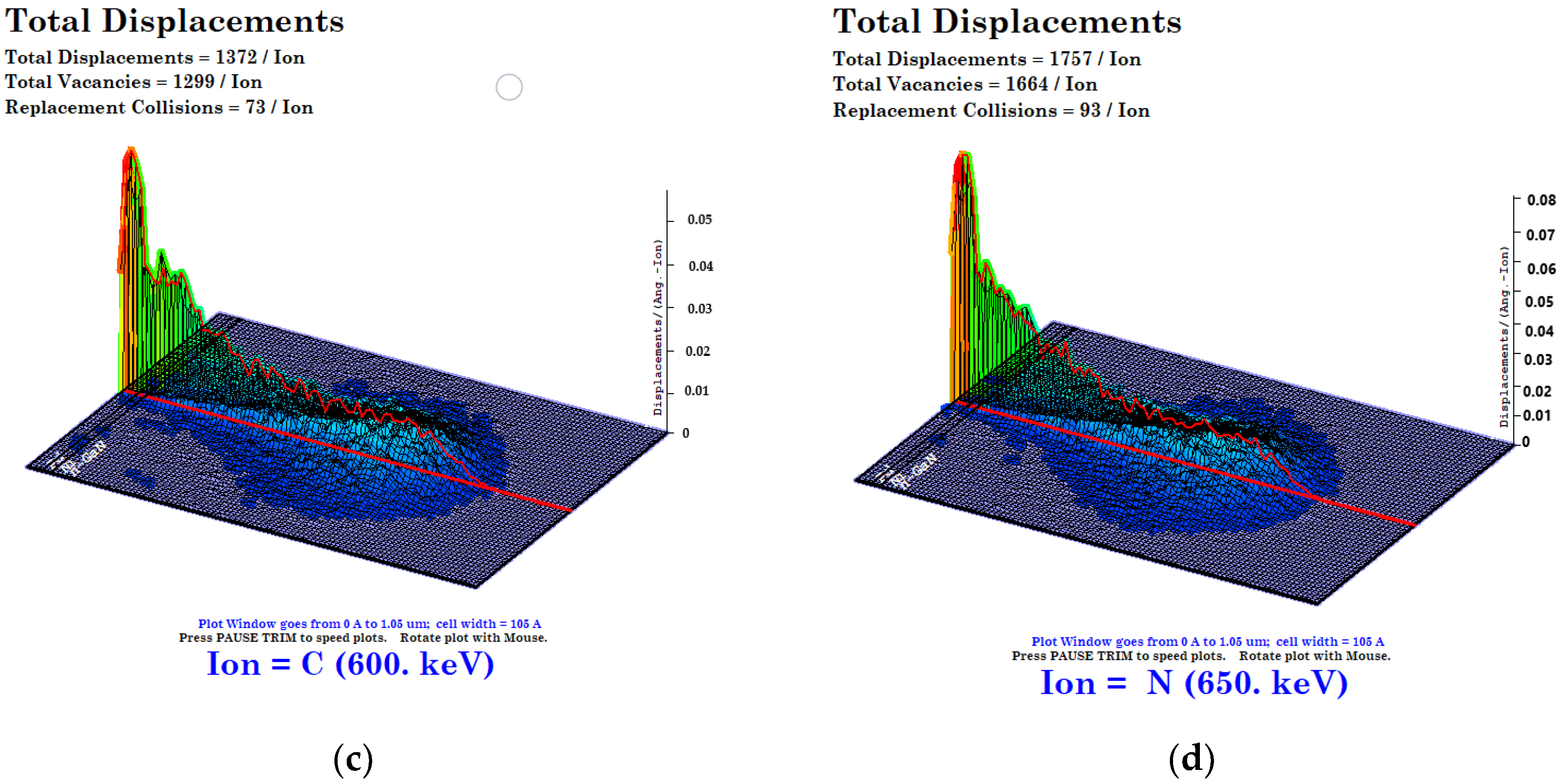
The stopping range, non-ionizing energy loss (NIEL), linear energy transfer (LET) and ionization displacement profile was calculated (Table 1) for 600 keV C2+ and 650 keV N2+ ion irradiation using SRIM and TRIM simulations [38]. The procedure followed for the estimation of damage profile, LET, and NIEL is mentioned elsewhere [39,40]. From Figure 1a–d, it is evident that for both 600 keV C2+ and 650 keV N2+ ions, the ionization damage is dominant in the beginning and it diminishes consequently before the ions stop in the substrate. The particle traverses through the device structure and stops deep inside the substrate. This indicates that ionization and displacement damages are at their maximum at the M-S interface and decrease along with the depth of the semiconductor material. Hence, a large number of displacements/vacancies are generated due to displacement damage and electron-hole pairs, which are created due to ionization damage. The enormous amount of LET induces both ionization and displacement damage. Total ionizing dose (TID) is a function of LET, and hence in the case of 600 keV C2+ and 650 keV N2+ ions, the ratio of nuclear energy loss (Sn) to electronic energy loss (Se) is found to be 3.1 × 10⁻² and 3.2 × 10⁻² respectively, which are comparable to each other. The fluence-dependent total ionizing dose (TID) and displacement damage (Dd) are tabulated in Table 2.

Table 1.
TRIM Calculations in GaN SBDs.
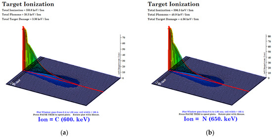
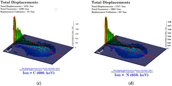
Figure 1.
(a) Distribution of ionization losses for 600 keV carbon ions in Ni/Pd/n-GaN SBDs; (b) Distribution of ionization losses for 650 keV nitrogen ions in Ni/Pd/n-GaN SBDs; (c) Distribution of displacement losses for 600 keV carbon ions in Ni/Pd/n-GaN SBDs; (d) Distribution of displacement losses for 650 keV nitrogen ions in Ni/Pd/n-GaN SBDs.

Table 2.
Fluence dependent TID and Dd for GaN SBDs.
3.2. Current-Voltage (I-V) Characteristics
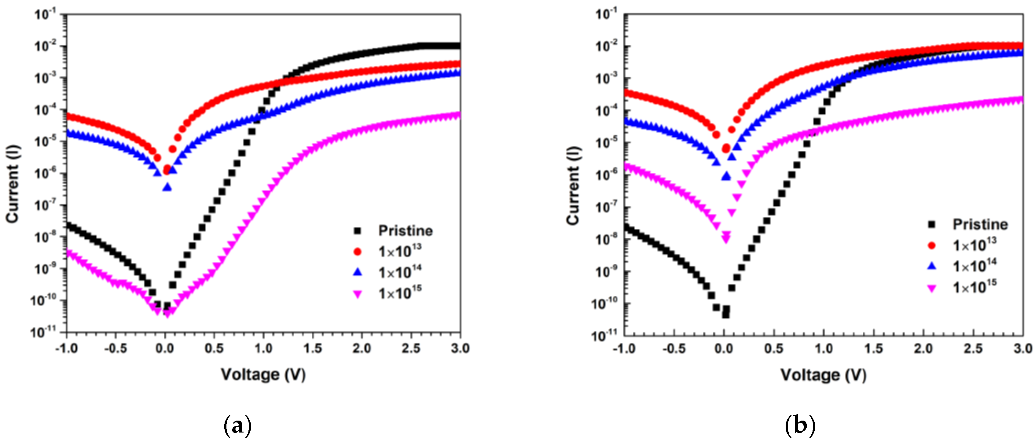
Room temperature I-V characteristics under MEI irradiation for different fluences (1 × 10¹³ to 1 × 10¹⁵ ions cm−2) are shown in Figure 2a,b, respectively.
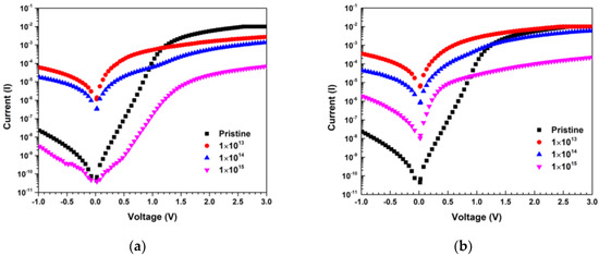
Figure 2.
(a) I-V Characteristics of Ni/Pd/n-GaN SBDs for different fluences of 600 keV C2+ ions; (b) I-V Characteristics of Ni/Pd/n-GaN SBDs for different fluences of 650 keV N2+ ions.
According to thermionic emission [41] theory, the rectifying metal-semiconductor (M-S) contacts show non-ideal I-V characteristics, given by
where the different symbols have their usual meanings [41].
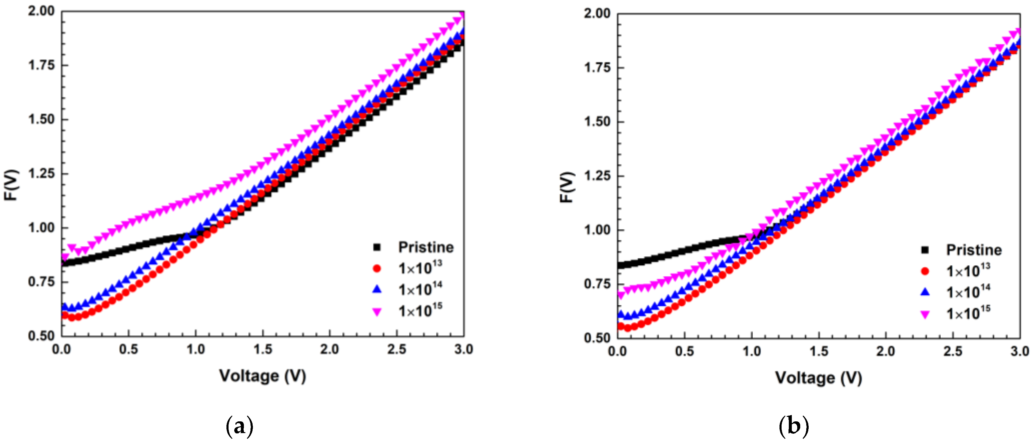
For the diodes with large series resistance (R), Norde [42] developed a method to determine φB and RS. Usually, the values of n lie between 1 and 2, so to determine large values of RS of diodes, the Norde’s method is used. Norde’s method involved the function F(V), given as
The current I0 corresponding to minima of F(V) vs. V plot will give RS as
and φB is given as
where F(V0) and V0 are the values of F(V) and V corresponding to the least value of current I0.
The extracted values of ideality factor (n), saturation current (I0) and barrier height (φB) from lnI vs. V plot and series resistance (RS) and barrier height (φB) values from Norde’s method [43] for different fluences of 600 keV C2+ and 650 keV N2+ ions from the graphs of F(V) vs. V. (Figure 3a,b) are reported in Table 3.
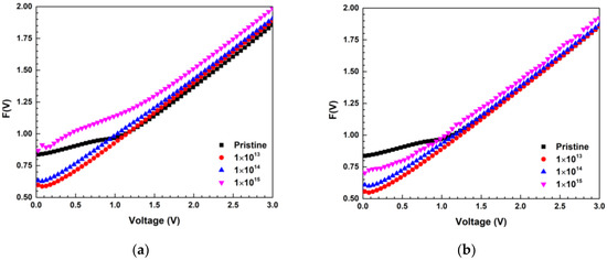
Figure 3.
(a) The F(V) vs. V plot of Ni/Pd/n-GaN SBDs for different fluences of 600 keV C2+ ions; (b) F(V) vs. V plot of Ni/Pd/n-GaN SBDs for different fluences of 650 keV N2+ ions.

Table 3.
The values of n, φB, RS, and I0 from Rhoderic and Norde method and reverse leakage current of Ni/Pd/n-GaN SBDs for different fluences of 600 keV C2+ and 650 keV N2+ ions.
At the lower fluences, RS decreases because of the increase in the carrier concentration due to the donor nature of carbon and nitrogen. Whereas at higher fluences, RS increases due to the evolution of various defect levels at different positions in the band-gap [44,45]. When the incident ion comes to rest in the semiconductor, a damaged layer is produced along its trajectory, which leads to increased values of RS [46]. The values of n are higher than unity for the pristine sample [36,47,48], which may be a result of the barrier inhomogeneities or due to tunneling and generation-recombination (G-R) currents, and it further increases with higher fluence due to increase in tunneling current. The reverse leakage current has increased significantly for the fluence of 1 × 10¹³ ions/cm2 of 600 keV C2+ and 650 keV N2+ ion irradiation. This increment in reverse leakage current occurs due to defects induced by 600 keV C2+ and 650 keV N2+ ion irradiation with deep energy levels in the middle of the forbidden gap which acts as generation-recombination (G-R) centers [49]. The displacements, vacancies introduced by 600 keV C2+ and 650 keV N2+ ion irradiation results in trap centers which leads to increase in thermal generation rate in the depletion region of the device. Thereafter there is a decrease in value of reverse leakage current along with the fluences confirms the increase of G-R centers [50]. The tunnelling of carriers through potential barriers by means of defect levels, i.e., defect assisted tunnelling significantly contributes to the increase in values of reverse leakage current. An increase in series resistance was found for higher irradiation fluences, demonstrating that the product of the mobility and carrier concentration has decreased. The decrease in mobility is due to the introduction of defect centers on irradiation, which act as scattering centers [40].
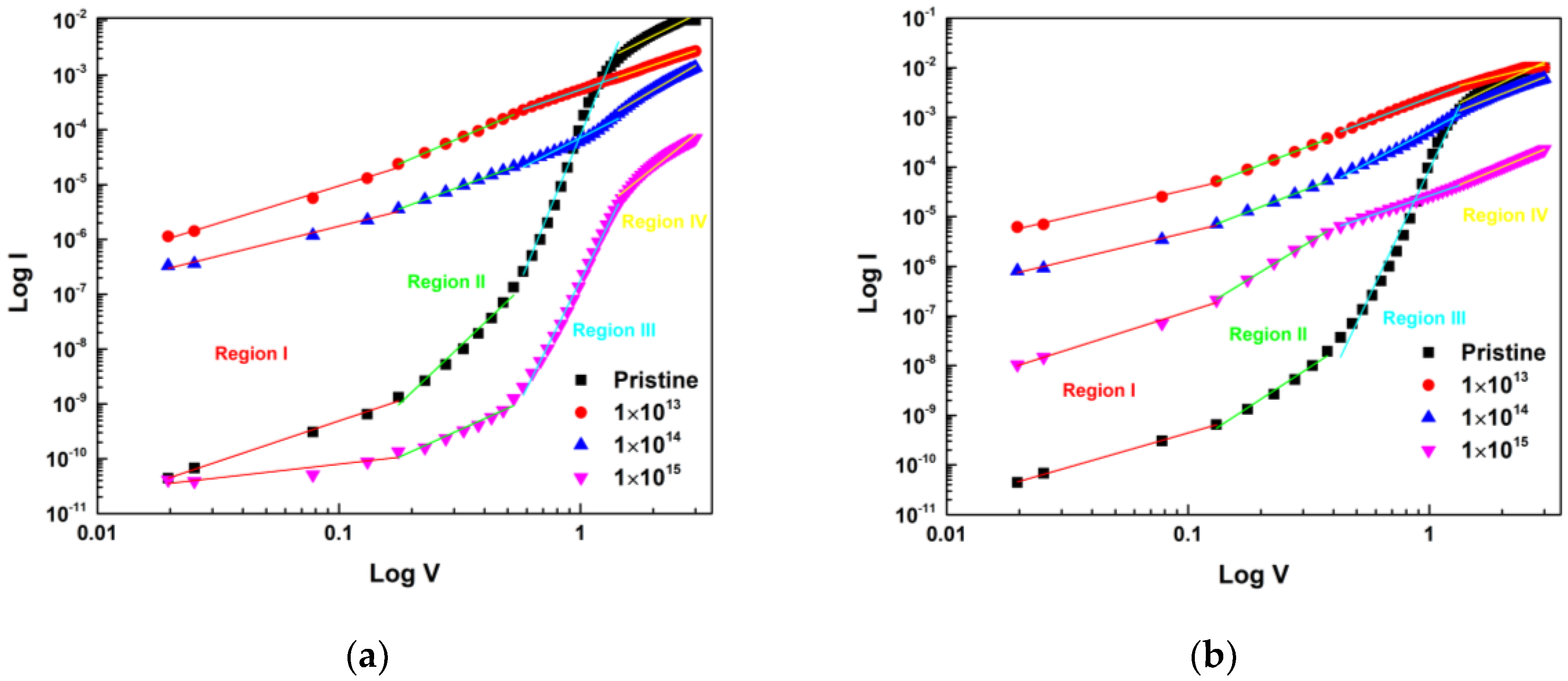
The current passing through an interface can have contributions from different current transport mechanisms such as thermionic emission, tunneling and G-R mechanisms [51]. These individual contributions are dependent upon the nature of ions and their energy and fluence. To investigate the dominant current conduction mechanism of the Ni/Pd/n-GaN SBDs under 600 keV C2+ and 650 keV N2+ ion irradiation in the forward-bias region of I-V characteristics, logI vs. logV was plotted and are shown in Figure 4a,b [52]. The forward bias logI vs. logV plot of the Ni/Pd/n-GaN SBDs shows a power-law behavior of the current as
where the exponent m values can be obtained from the slope of Figure 4a,b. The slope values m, indicate the different forward current conduction mechanisms of the device.
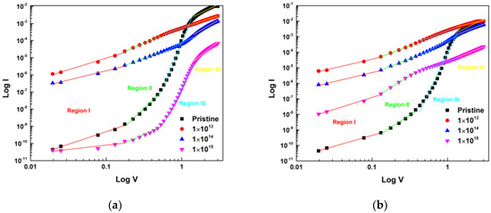
Figure 4.
(a) The logI vs. logV plot of Ni/Pd/n-GaN SBDs for different fluences of 600 keV C2+ ions; (b) The logI vs. logV plot of Ni/Pd/n-GaN SBDs for different fluences of 650 keV N2+ ions.
Here we can observe that logI vs. logV plot has four linear regions corresponding to low voltage region (I), intermediate voltage region (II and III), and high voltage region (IV) with different slopes given in Table 4, which shows the presence of various conduction mechanisms whereas the values of slope are found to be 1.48 (region I), 4.19 (region II), 10.76 (region III), and 2.18 (region IV) for the Ni/Pd/n-GaN SBDs, respectively. From the values of slope in region I, it is evident that the current conductions in the low bias region for the Ni/Pd/n-GaN SBDs exhibit an ohmic behavior because of existing background doping or thermally generated carriers [53]. In regions II and III, the slope estimations of the Ni/Pd/n-GaN SBDs are greater than two, indicating that the charge transport is governed by the trap-charge limited current (TCLC) due to the increase in the number of injected electrons which leads to filling up the traps [54]. At higher voltages (region IV), the values of slope tend to decrease as devices approach the “trap-filled limit”. This is a result of the strong electron injection; the electrons escape from the traps, which add to “space-charge-limited current (SCLC)” [55,56]. Obviously, at high voltages it reaches a trap-filled state and current conduction can be described by the trap-free Mott-Gurney law [57,58].

Table 4.
The slope from the logI vs. logV plot of Ni/Pd/n-GaN SBDs for different fluences of 600 keV C2+ and 650 keV N2+ ions.
When the devices are exposed to 600 keV C2+ and 650 keV N2+ ion irradiation, the displacement and ionization damages are created along the trajectory of the ion beam, as is evident from the SRIM/TRIM simulations. This is reflected in the electrical characteristics of the device. For the low fluence of 600 keV C2+ and 650 keV N2+ ion irradiation, the slope of all four regions decreases, which may be due to the donor behavior of C2+ & N2+, which leads to filling up the traps and increasing the space charges. Whereas for the intermediate and highest fluences of 600 keV C2+ and 650 keV N2+ ion irradiation, the value of the slopes of regions II, III, and IV is continuously increasing, which may be due to the creation of defects, which act as traps, and charge transport is governed by the TCLC. The TCLC is more dominant for C2+ ions as compared to N2+ ions for the highest fluence, which may be due to the greater amount of damage caused by C2+ than N2+ ions in the device.
The reverse current conduction mechanism for 600 keV C2+ and 650 keV N2+ ion irradiation of Ni/Pd/n-GaN SBDs studied at room temperature by considering Poole–Frenkel emission (PFE) and Schottky emission (SE) mechanisms across the junction. The reverse current, when dominated by PFE mechanism, is given by [59]
and when the current is dominated by SE mechanism, it is given by
where βPF and βSE are the PFE and SE field lowering coefficients, respectively. The theoretical values for βPF and βSE are given by
The theoretical values of field lowering coefficients for Ni/Pd/n-GaN SBDs are βPF = 2.54 × 10⁻⁵ eVm1/2 V −1/2 and βSE = 1.27 × 10⁻⁵ eVm1/2 V −1/2.
From the plots of ln (IR) vs. V1/2 (Figure 5a,b), the dominant reverse current transport mechanism is determined for MEI irradiation of Ni/Pd/n-GaN SBDs for different fluences at room temperature.
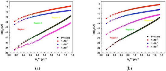
Figure 5.
(a) The plots of ln (IR) vs. V1/2 of Ni/Pd/n-GaN SBDs for different fluences of 600 keV C2+ ions; (b) The plots of ln (IR) vs. V1/2 of Ni/Pd/n-GaN SBDs for different fluences of 650 keV N2+ ions.
The results show (Table 5) that the reverse current conduction mechanism of Ni/Pd/n-GaN SBDs corresponds to PFE in the regions I, II, and III for pristine. This indicates that the carrier transport occurs from the metal into the conductive dislocation that occurred via a trapped state [60]. Then it changes to SE, which increases along with a fluence of 1 × 10¹³ ions cm−2 for irradiation with 600 keV C2+ and 650 keV N2+ ions due to the donor behavior of C2+/N2+ ions, which might have filled the trap states. Meanwhile, for higher fluences of C2+/N2+ ion irradiation, in region II and region III, the reverse current conduction mechanism of Ni/Pd/n-GaN SBDs corresponding to PFE may be due to the creation of defects which act as traps. Also, the PFE is more dominant for C2+ ions than for N2+ ions for the highest fluence, which may be due to the creation of a greater amount of damage by the C2+ ions than the N2+ ions in the Ni/Pd/n-GaN SBDs.

Table 5.
The experimental values of βPF and βSE of Ni/Pd/n-GaN SBDs are for different fluences of 600 keV C2+ and 650 keV N2+ ions.
3.3. Capacitance-Voltage (C-V) Characteristics
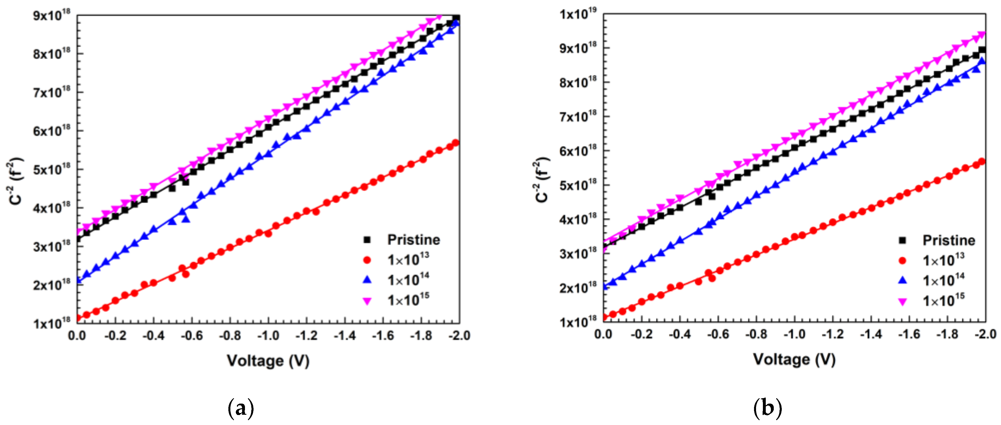
The capacitance of MEI-irradiated Ni/Pd/n-GaN SBDs was measured as a function of junction voltage at a constant frequency of 1MHz. Figure 6a,b shows the variation of C−2 with the applied voltage of Ni/Pd/n-GaN SBDs, respectively, at room temperature for different fluences.

Figure 6.
(a) The plots of C−2 vs. V of Ni/Pd/n-GaN SBDs for different fluences of 600 keV C2+ ions; (b) The plots of C−2 vs. V of Ni/Pd/n-GaN SBDs for different fluences of 650 keV N2+ ions.
When a voltage V is applied to a junction, the capacitance of the depletion layer is given by [61]
where the different symbols have their usual meanings [61].
The x-intercept (V0) of the C−2 vs. V plot is related to the built-in potential (Vi), and the barrier height (φB) is given by
The calculated values of φB and dopant concentration (Nd) are given in Table 6.

Table 6.
The values of φB and Nd of Ni/Pd/n-GaN SBDs for different fluences of 600 keV C2+ and 650 keV N2+ ions.
The values of φB calculated by the I-V technique are smaller than the values extracted by the C-V technique. The presence of the native oxide (Ga2O3) layer at the M-S interface influences the I-V characteristics significantly [2,25]. All damage at the M-S interface changes the I-V characteristics since defects may act as recombination centers or traps for trap-assisted tunnel currents. Since the capacitance of the depletion layer is in series with the capacitance of the interfacial layer, the C-V measurements are less affected than I-V measurements. As I-V techniques involve the flow of electrons from semiconductor to metal, the barrier height extracted from this method will give lower value than from C-V measurements. This might be due to the image force lowering of the barrier height, whereas the value obtained from the capacitance measurement is not affected by image force [62]. In the present case, it might be because of the barrier inhomogeneities present at the M-S interface and the introduction of interfacial defects via displacement damage due to MEI irradiation [56,61]. The dopant concentration increases for the lowest fluence of 600 keV C2+ and 650 keV N2+ ions irradiation. From TRIM simulations, the ionization and displacement damage for 600 keV C2+ ions are 558.0 keV/ion, and 3.56 keV/ion, respectively, whereas for 650 keV N2+ ions their values are 596.0 keV/ion, and 4.56 keV/ion, respectively. Therefore, due to the lower value of Sn, they cause less displacement damage as compared to ionization across the interface. This also leads to a significant decrease in the values of Schottky barrier height. Meanwhile, with higher fluence, the damage produced by avalanches will start overlapping, and several nontrivial effects may result. However, the increase in donor concentration at 1 × 10¹³ fluence is consistent with I-V data. The effective donor concentration may decrease with an increase in influence due to a possible increase in trap states due to defects. Here it is essential to take note that the I-V and C-V data are consistent with each other.
3.4. Photoluminescence (PL)
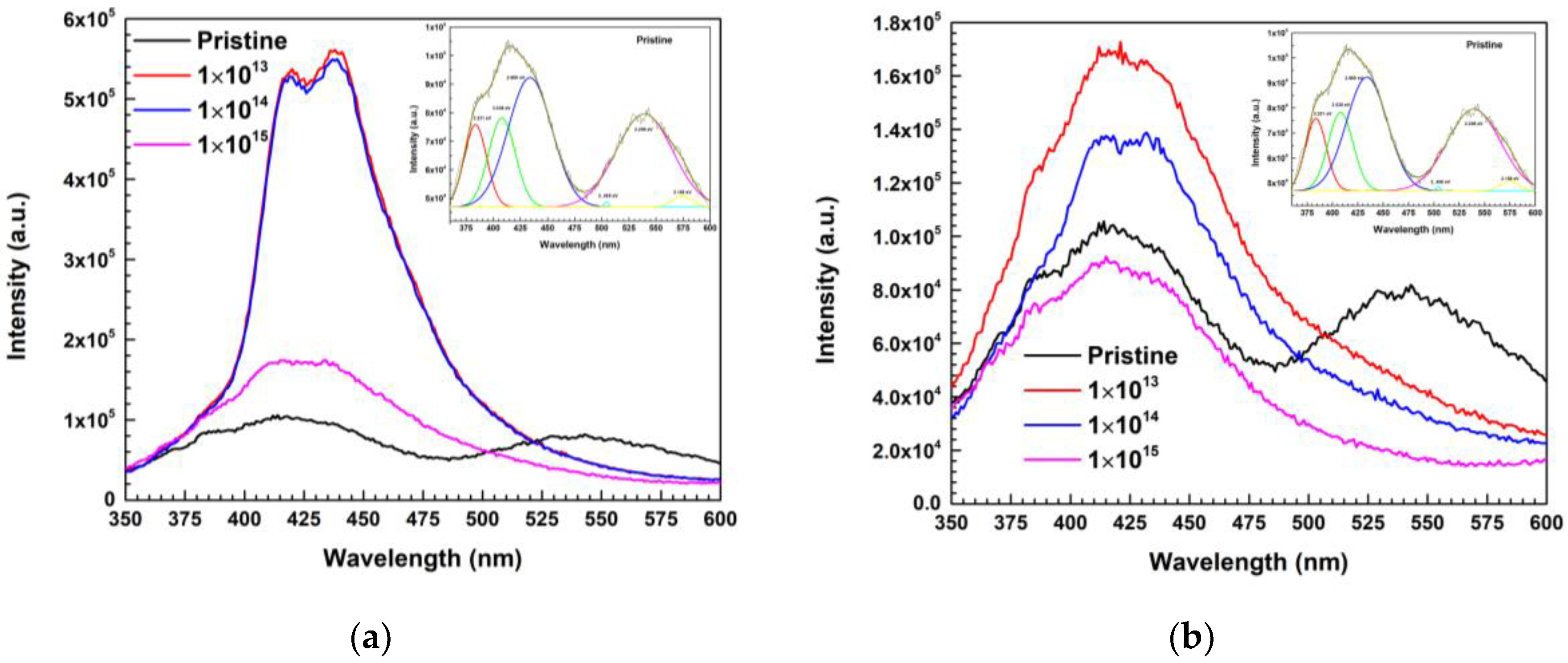
The optically active interface defect states and their evolution during MEI irradiation were investigated based on PL characterizations performed at room temperature. PL spectra of 600 keV C2+ and 650 keV N2+ ions irradiated Ni/Pd/n-GaN SBDs are shown in Figure 7a,b.

Figure 7.
(a) The PL spectra of Ni/Pd/n-GaN SBDs for different fluences of 600 keV C2+ ions; (b) The PL spectra of Ni/Pd/n-GaN SBDs for different fluences of 650 keV N2+ ions.
The presence of Ga and N vacancies or deep-level impurities and amorphous phases in the pristine sample may be the reason for violet {VL (383.73 nm, 408.11 nm, 433.51 nm)}, cyan {CL (504.41 nm)}, green {GL (539.29 nm)} and yellow luminescence {YL (574.53 nm)} [9,63,64]. VL and CL increase for a fluence of 1 × 10¹³ ions cm−2 of 600 keV C2+ and 650 keV N2+ ion irradiation and steadily decreases with higher fluences, whereas YL vanishes in both the cases. Apart from that, BL (437.79 nm, 446.78 nm) evolved with a fluence of 1 × 10¹³ ions cm−2 of 600 keV C2+ and 650 keV N2+ ion irradiation and increased with average fluence, followed by a decline in the intensity of BL. Additionally, GL disappears for 1 × 10¹⁵ fluences of C2+ ion irradiation, whereas it decreases steadily with N2+ ion irradiation. This might be because of the donor behavior of C2+ ions and N2+ ions, which occupies the Ga vacancies and leads to the vanishing of YL and increases of VL, BL, CL, and GL at moderate fluences, and decreases afterward due to radiation damage [64,65,66,67]. The existence of GL luminescence may be expected due to the combination of gallium vacancy clusters and impurities (C2+/N2+) due to ion irradiation, which is bound to dislocations [67,68]. The results of PL are consistent with I-V and C-V data, reconfirming the observation that C/N are acting as donors at lower fluences.
3.5. X-Ray Diffraction (XRD)
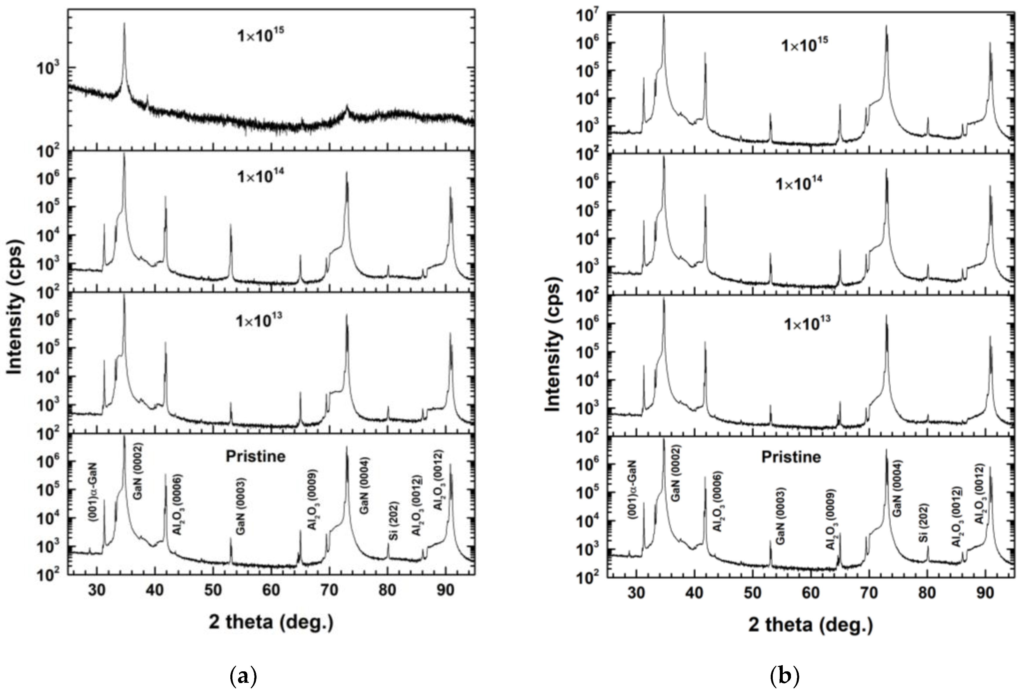
The effect of MEI irradiation on the structural modifications at the Ni/Pd/n-GaN SBDs interface were investigated based on comparative XRD analysis, as shown in Figure 8a,b, covering from 25 to 95 degrees.

Figure 8.
(a) The XRD pattern of Ni/Pd/n-GaN SBDs for different fluences of 600 keV C2+ ions; (b) The XRD pattern of Ni/Pd/n-GaN SBDs for different fluences of 650 keV N2+ ions.
The results show that there are well-defined diffraction peaks of GaN (0002), Al2O3(0006), GaN (0003), Al2O3(0009), GaN (0004), Al2O3(0012), Al2O3(0012), Si (202) in the pristine sample [69,70,71]. MEI irradiation broadened the peaks of GaN (0002), Al2O3(0006) and GaN (0004). Also, there is no indication of any secondary phase formation in the MEI irradiated samples, which might be expected to be because of the high displacement damage introduced by ion irradiation [71,72]. The diffraction peaks are broadened, and a shift in the values of two thetas towards the lower side can be observed as the fluence of 600 keV C2+ and 650 keV N2+ ion irradiation is increased. Ion irradiation introduces lattice disorder into crystalline GaN, due to the expansion of which in the GaN peak, new peaks corresponding to the damaged section of the lattice evolved on the low theta side of the main GaN peak in the XRD spectra of the irradiated GaN [26,73,74]. Furthermore, it was observed that for higher fluences of C2+ ion irradiation, the dislocation density increased, leading to higher damage as compared to N2+ ion irradiation. The decrease in the intensity of C2+ ion irradiation is higher than that for N2+ ion irradiation, which may be due to the change in the mean atomic scattering factor at a given site for light C2+ ions as compared to N2+ ions [75,76]. Additionally, the peaks, except for GaN (0002), entirely disappear for the fluence of 1 × 10¹⁵ ions cm−2 of 600 keV C2+ ions, indicating that the GaN lattice is disordered, which might lead to the formation of a surface amorphous layer, whereas in the literature the formation of the surface amorphous layer has previously been reported for a fluence of 1 × 10¹⁷ ions cm−2 [77,78,79]. In the present case, ions are implanted in the device structure interstitially, leading to lattice deformations and the generation of defects. In the linear avalanche regime, the damage build-up might follow defect accumulation up to a critical defect density, and in the displacement avalanche regime, a disordered vicinity such as amorphization would arise because of direct ion impact mechanism [80]. Morehead and Crowder [81] proposed a model that hypothesized that each ion hitting the target produces a cylindrical amorphous core. Amorphization happens when such damage cores fill the area of the target. The critical fluence for amorphization decreases with increasing ion mass according to this semi-quantitative model. As nitrogen mass is higher than carbon, the amorphization is observed at a fluence of 1 × 10¹⁵ of C2+ ion, whereas there is no such type of observation for N2+ ion.
4. Discussion
The current transport properties of Ni/Pd/n-GaN SBDs were investigated for 600 keV C2+ and 650 keV N2+ ions in the fluence range of 1 × 10¹³ to 1 × 10¹⁵ ions cm−2 at room temperature. The electrical parameters such as ideality factor (n), series resistance (RS), and barrier height (φB) were calculated using the I-V and C-V techniques. The increase in the value of n along with higher fluences of MEI irradiation may be due to the activation of multiple transport mechanisms. The values of φB and RS decrease for a fluence of 1 × 10¹³ ions cm−2 and increase further for higher fluences of MEI irradiation. The contributions of various current transport mechanisms, including defect-assisted tunneling and G-R currents along with thermionic emission mechanisms might have significantly influenced the changes in values of φB and RS. Usually, ion irradiation decreases the carrier mobility and carrier concentration and enhances the series resistance, which was also observed in the C-V analysis. MEI irradiation introduced a significant number of displacements and vacancies, which was also validated by the SRIM and TRIM calculations, and these defects increased the series resistance by decreasing the minority carrier [55]. Ionization and displacement damage profile simulations showed that the displacement damage was dominant in the bulk GaN. Additionally, 600 keV C2+ and 650 keV N2+ ions showed higher contributions of tunneling currents, as observed from the higher forward currents than reverse currents for fluences of 1 × 10¹³ to 1 × 10¹⁵ ions cm−2. The ratios of nuclear energy loss (Sn) to electronic energy loss (Se) for 600 keV C2+ and 650 keV N2+ ions were comparable. This suggests that due to high nuclear energy loss, more displacement damage is created in the lattice, leading to massive contributions from defect-assisted tunneling currents [26].
Furthermore, the reverse current conduction mechanism of the Ni/Pd/n-GaN SBDs is PFE for lower reverse voltages and it changes to SE for higher fluences. Meanwhile, for higher reverse voltage, it was mainly SE and increased with higher fluences. The XRD analysis exhibited a broadening of peaks at higher fluences of 600 keV C2+ and 650 keV N2+ ions, which indicates the high degree of displacement damage created due to irradiation. At fluence 1 × 10¹⁵ ions cm−2 of 600 keV C2+ ions, the SBD showed an increase in ideality factor (n), and XRD showed structural degradation in Ni/Pd/n-GaN SBD, which were attributed to ion-induced damage in the form of point defects. Overall, C2+ and N2+ ion irradiation introduced similar damage in electrical characterization, whereas C2+ ion irradiation resulted in significantly higher structural damage compared to N2+ ion irradiation, which is evident from XRD. Additionally, PL characteristics of Ni/Pd/n-GaN SBDs for MEI irradiation indicate that at higher fluences yellow luminescence disappears, which is a signature of donor behavior of 600 keV C2+ and 650 keV N2+ ions, which occupies the Ga vacancies. Meanwhile, the green luminescence corresponds to the dislocation caused by MEI irradiation.
5. Conclusions
600 keV C2+ and 650 keV N2+ ion irradiation significantly altered the charge transport, structural and optical properties of Ni/Pd/n-GaN SBDs. The deviation in electrical parameters are correlated with the defects and the damage profiles estimated through SRIM/TRIM simulation, which are exceptionally reliant upon the fluences of MEI. Similarly, we affirmed that the charge transport mechanism is affected by additional defects at higher fluences due to the contributions of various other current transport mechanisms along with the thermionic emission mechanism. PL observation confirms that C/N act as donors at lower fluences, which is also validated by I-V and C-V measurements. From the XRD results, we conclude that structural damage in Ni/Pd/n-GaN SBDs is higher for 600 keV C2+ than 650 keV N2+ ions for a fluence of 1 × 10¹⁵ ions cm−2 which leads to the amorphization which is validated by semi-quantitative model.
Author Contributions
Conceptualization, K.S., S.K., V.K.M., and A.K.; methodology, K.S., S.K., V.K.M., A.K., V.R.R. and S.V.S.N.R.; validation, K.S., S.K. and V.K.M.; formal analysis, S.K.; investigation, K.S., S.K., V.K.M. and A.N.; writing—original draft preparation, K.S., S.K., V.K.M.; writing—review and editing, K.S., S.K., V.K.M., V.R.R., S.V.S.N.R., J.T., S.R., X.Z. and A.N.; visualization, K.S., S.K., V.K.M., V.R.R., S.V.S.N.R., J.T. and X.Z.; supervision, K.S. All authors have read and agreed to the published version of the manuscript.
Funding
This research received no external funding.
Acknowledgments
The authors are thankful to IUAC, New Delhi, India, for providing a Low Energy Beam Ion irradiation facility and IV and CV measurement facilities. The authors are also grateful to the Central facility for nanotechnology (CFN), the University of Hyderabad, and School of Physics (UGC-NRC) for providing access to necessary experimental facilities.
Conflicts of Interest
The authors declare no conflict of interest.
References
- Kumar, A.; Asokan, K.; Kumar, V.; Singh, R. Temperature dependence of 1/f noise in Ni/n-GaN Schottky barrier diode. J. Appl. Phys. 2012, 112, 024507. [Google Scholar] [CrossRef]
- Rideout, V.L. A review of the theory and technology for ohmic contacts to group III–V compound semiconductors. Solid State Electron. 1975, 18, 541–550. [Google Scholar] [CrossRef]
- Omotoso, E.; Meyer, W.E.; Auret, F.D.; Paradzah, A.T.; Diale, M.; Coelho, S.M.; van Rensburg, P.J. The influence of high energy electron irradiation on the Schottky barrier height and the Richardson constant of Ni/4H-SiC Schottky diodes. Mater. Sci. Semicond. Process. 2015, 39, 112–118. [Google Scholar] [CrossRef]
- Omotoso, E.; Meyer, W.E.; van Rensburg, P.J.; Igumbor, E.; Tunhuma, S.M.; Ngoepe, P.N.M.; Danga, H.T.; Auret, F.D. The effects of high-energy proton irradiation on the electrical characteristics of Au/Ni/4H-SiC Schottky barrier diodes. Nucl. Instrum. Methods Phys. Res. Sect. B Beam Interact. Mater. At. 2017, 409, 241–245. [Google Scholar] [CrossRef]
- Millán, J.; Godignon, P.; Perpiñà, X.; Pérez-Tomás, A.; Rebollo, J. A survey of wide bandgap power semiconductor devices. IEEE Trans. Power Electron. 2013, 29, 2155–2163. [Google Scholar] [CrossRef]
- Zhang, Y.; Debelle, A.; Boulle, A.; Kluth, P.; Tuomisto, F. Advanced techniques for characterization of ion beam modified materials. Curr. Opin. Solid State Mater. Sci. 2015, 19, 19–28. [Google Scholar] [CrossRef]
- Sun, Y.; Kang, X.; Zheng, Y.; Lu, J.; Tian, X.; Wei, K.; Wu, H.; Wang, W.; Liu, X.; Zhang, G. Review of the recent progress on GaN-based vertical power Schottky barrier diodes (SBDs). Electronics 2019, 8, 575. [Google Scholar] [CrossRef]
- Liang, F.; Zhao, D.; Jiang, D.; Liu, Z.; Zhu, J.; Chen, P.; Yang, J.; Liu, S.; Xing, Y.; Zhang, L. Role of Si and C Impurities in Yellow and Blue Luminescence of Unintentionally and Si-Doped GaN. Nanomaterials 2018, 8, 1026. [Google Scholar] [CrossRef] [PubMed]
- Santana, G.; De Melo, O.; Aguilar-Hernández, J.; Mendoza-Pérez, R.; Monroy, B.; Escamilla-Esquivel, A.; López-López, M.; De Moure, F.; Hernández, L.; Contreras-Puente, G. Photoluminescence study of gallium nitride thin films obtained by infrared close space vapor transport. Materials 2013, 6, 1050–1060. [Google Scholar] [CrossRef] [PubMed]
- Lee, M.; Vu, T.; Lee, K.; Kim, E.; Park, S. Electronic Transport Mechanism for Schottky Diodes Formed by Au/HVPE a-Plane GaN Templates Grown via In Situ GaN Nanodot Formation. Nanomaterials 2018, 8, 397. [Google Scholar] [CrossRef] [PubMed]
- Son, K.; Liao, A.; Lung, G.; Gallegos, M.; Hatake, T.; Harris, R.D.; Scheick, L.Z.; Smythe, W.D. GaN-based high temperature and radiation-hard electronics for harsh environments. Nanosci. Nanotechnol. Lett. 2010, 2, 89–95. [Google Scholar] [CrossRef]
- Dalla Vecchia, M.; Ravyts, S.; Van den Broeck, G.; Driesen, J. Gallium-Nitride Semiconductor Technology and Its Practical Design Challenges in Power Electronics Applications: An Overview. Energies 2019, 12, 2663. [Google Scholar] [CrossRef]
- Ahmad, I.; Akram, W. Introductory Chapter: Introduction to Ion Implantation. In Ion Implantation-Research and Application; IntechOpen: London, UK, 2017. [Google Scholar]
- Williams, J.S. Ion implantation of semiconductors. Mater. Sci. Eng. A 1998, 253, 8–15. [Google Scholar] [CrossRef]
- Newell, P.T.; Meng, C.-I. Ion acceleration at the equatorward edge of the cusp: Low altitude observations of patchy merging. Geophys. Res. Lett. 1991, 18, 1829–1832. [Google Scholar] [CrossRef]
- Thomé, L.; Debelle, A.; Garrido, F.; Mylonas, S.; Décamps, B.; Bachelet, C.; Sattonnay, G.; Moll, S.; Pellegrino, S.; Miro, S. Radiation effects in nuclear materials: Role of nuclear and electronic energy losses and their synergy. Nucl. Instrum. Methods Phys. Res. Sect. B Beam Interact. Mater. At. 2013, 307, 43–48. [Google Scholar] [CrossRef]
- Qi, Q.; Cheng, G.J.; Shi, L.Q.; O’Connor, D.J.; King, B.V.; Kisi, E.H. Damage accumulation and recovery in C+-irradiated Ti3SiC2. Acta Mater. 2014, 66, 317–325. [Google Scholar] [CrossRef]
- Knetzger, M.; Meissner, E.; Schröter, C.; Friedrich, J. Theoretical aspects and microstructural investigations on V-pit defects in HVPE grown GaN. J. Cryst. Growth 2019, 518, 51–58. [Google Scholar] [CrossRef]
- Pearton, S.J.; Ren, F.; Patrick, E.; Law, M.E.; Polyakov, A.Y. Ionizing radiation damage effects on GaN devices. Ecs J. Solid State Sci. Technol. 2016, 5, Q35–Q60. [Google Scholar] [CrossRef]
- Pearton, S.J.; Deist, R.; Ren, F.; Liu, L.; Polyakov, A.Y.; Kim, J. Review of radiation damage in GaN-based materials and devices. J. Vac. Sci. Technol. A Vac. Surf. Film. 2013, 31, 050801. [Google Scholar] [CrossRef]
- Kumar, A.; Dhillon, J.; Verma, S.; Kumar, P.; Asokan, K.; Kanjilal, D. Identification of swift heavy ion induced defects in Pt/n-GaN Schottky diodes by in-situ deep level transient spectroscopy. Semicond. Sci. Technol. 2018, 33, 085008. [Google Scholar] [CrossRef]
- Kumar, A.; Singh, R.; Kumar, P.; Singh, U.B.; Asokan, K.; Karaseov, P.A.; Titov, A.I.; Kanjilal, D. In-situ transport and microstructural evolution in GaN Schottky diodes and epilayers exposed to swift heavy ion irradiation. J. Appl. Phys. 2018, 123, 161539. [Google Scholar] [CrossRef]
- Zhang, L.Q.; Zhang, C.H.; Li, J.J.; Meng, Y.C.; Yang, Y.T.; Song, Y.; Ding, Z.N.; Yan, T.X. Damage to epitaxial GaN layer on Al 2 O 3 by 290-MeV 238 U 32+ ions irradiation. Sci. Rep. 2018, 8, 1–10. [Google Scholar]
- Karlušić, M.; Kozubek, R.; Lebius, H.; Ban-d’Etat, B.; Wilhelm, R.A.; Buljan, M.; Siketić, Z.; Scholz, F.; Meisch, T.; Jakšić, M. Response of GaN to energetic ion irradiation: Conditions for ion track formation. J. Phys. D Appl. Phys. 2015, 48, 325304. [Google Scholar] [CrossRef]
- Kucheyev, S.O.; Williams, J.S.; Pearton, S.J. Ion implantation into GaN. Mater. Sci. Eng. R Rep. 2001, 33, 51–108. [Google Scholar] [CrossRef]
- Ding, F.R.; He, W.H.; Vantomme, A.; Zhao, Q.; Pipeleers, B.; Jacobs, K.; Moerman, I. Lattice expansion induced by Zn channeled implantation in GaN. Mater. Sci. Semicond. Process. 2002, 5, 511–514. [Google Scholar] [CrossRef]
- Li, B.S.; Liu, H.P.; Xu, L.J.; Wang, J.; Song, J.; Peng, D.P.; Li, J.H.; Zhao, F.Q.; Kang, L.; Zhang, T.M. Lattice disorder and N elemental segregation in ion implanted GaN epilayer. Appl. Surf. Sci. 2020, 499, 143911. [Google Scholar] [CrossRef]
- Kumar, D.R.; Ranjith, K.S.; Nivedita, L.R.; Asokan, K.; Kumar, R.R. Swift heavy ion induced effects on structural, optical and photo-catalytic properties of Ag irradiated vertically aligned ZnO nanorod arrays. Nucl. Instrum. Methods Phys. Res. Sect. B Beam Interact. Mater. At. 2019, 450, 95–99. [Google Scholar] [CrossRef]
- Duboz, J.-Y.; Zucchi, J.; Frayssinet, E.; Chalbet, P.; Chenot, S.; Hugues, M.; Grini, J.-C.; Vidal, M.; Herault, J. GaN Schottky diodes for proton beam monitoring. Biomed. Phys. Eng. Express 2018, 5, 025015. [Google Scholar] [CrossRef]
- Baskar, K. Shodhganga, MOCVD Growth and Characterization of InGaN and InGaN GaN Quantumwell Structures and Effect of Ion Irradiation. 2018. Available online: http://shodhganga.inflibnet.ac.in:8080/jspui/handle/10603/234176 (accessed on 17 November 2019).
- Titov, A.I.; Karabeshkin, K.V.; Karaseov, P.A.; Struchkov, A.I. Do Chemical Effects Affect the Accumulation of Structural Damage during the Implantation of Fluorine Ions into GaN? Semiconductors 2019, 53, 1415–1418. [Google Scholar] [CrossRef]
- Ngoepe, P.N.M.; Meyer, W.E.; Auret, F.D.; Omotoso, E.; Hlatshwayo, T.T.; Diale, M. Characterisation of Cs ion implanted GaN by DLTS. Phys. B Condens. Matter 2018, 535, 96–98. [Google Scholar] [CrossRef]
- Yoshino, M.; Sugamata, K.; Ikeda, K.; Nishimura, T.; Kuriyama, K.; Nakamura, T. Ion implanted GaN MISFETs fabricated in Mg implanted layers activated by conventional rapid thermal annealing. Nucl. Instrum. Methods Phys. Res. Sect. B Beam Interact. Mater. At. 2019, 449, 49–53. [Google Scholar] [CrossRef]
- Macková, A.; Malinský, P.; Jágerová, A.; Sofer, Z.; Sedmidubský, D.; Klímová, K.; Böttger, R.; Akhmadaliev, S. Damage accumulation and structural modification in a-and c-plane GaN implanted with 400-keV and 5-MeV Au+ ions. Surf. Interface Anal. 2018, 50, 1099–1105. [Google Scholar] [CrossRef]
- Lei, Z.F.; Guo, H.X.; Tang, M.H.; Zeng, C.; Zhang, Z.G.; Chen, H.; En, Y.F.; Huang, Y.; Chen, Y.Q.; Peng, C. Degradation mechanisms of AlGaN/GaN HEMTs under 800 MeV Bi ions irradiation. Microelectron. Reliab. 2018, 80, 312–316. [Google Scholar] [CrossRef]
- Reddy, M.S.P.; Kumar, A.A.; Reddy, V.R. Electrical transport characteristics of Ni/Pd/n-GaN Schottky barrier diodes as a function of temperature. Thin Solid Film. 2011, 519, 3844–3850. [Google Scholar] [CrossRef]
- Plante, J. Alternative Test Methods for Electronic Parts. NEPP, 2004. Available online: https://www.google.com/search?sxsrf=ACYBGNTB1bBEh47D_ZH76g5LO77HX6s4ug%3A1582113514934&ei=6iJNXtPLOMXIyAPmv4O4AQ&q=Plante%2C+J.++Alternative+test+methods+for+electronic+parts.+2004.&oq=Plante%2C+J.++Alternative+test+methods+for+electronic+parts.+2004.&gs_l=psy-ab.3...2391.2989..3747...0.2..1.354.998.0j1j2j1......0....1..gws-wiz.......0i71.BhWDBlfkRXU&ved=0ahUKEwjT6LSQyN3nAhVFJHIKHebfABcQ4dUDCAs&uact=5 (accessed on 10 November 2019).
- Stoller, R.E.; Toloczko, M.B.; Was, G.S.; Certain, A.G.; Dwaraknath, S.; Garner, F.A. On the use of SRIM for computing radiation damage exposure. Nucl. Instrum. Methods Phys. Res. Sect. B Beam Interact. Mater. At. 2013, 310, 75–80. [Google Scholar] [CrossRef]
- Kumar, M.V.; Verma, S.; Shobha, V.; Jayashree, B.; Kanjilal, D.; Krishnaveni, S. 100 MeV Si^ sup 7+^ Ion Irradiation Induced Modifications in Electrical Characteristics of Si Photo Detector: An In-Situ Reliability Study. J. Mater. Sci. Res. 2014, 3, 24. [Google Scholar]
- Kumar, M.V.; Verma, S.; Asokan, K.; Shobha, V.; Karanth, S.P.; Krishnaveni, S. In Situ Electrical Characteristics of 150 MeV Ag9+ Ion Beam Induced Damage in Si Photo Detector. ECS J. Solid State Sci. Technol. 2016, 5, P384–P388. [Google Scholar] [CrossRef]
- Herring, C.; Nichols, M.H. Thermionic emission. Rev. Mod. Phys. 1949, 21, 185. [Google Scholar] [CrossRef]
- Norde, H. A modified forward I-V plot for Schottky diodes with high series resistance. J. Appl. Phys. 1979, 50, 5052–5053. [Google Scholar] [CrossRef]
- Lien, C.-D.; So, F.C.T.; Nicolet, M.-A. An improved forward IV method for nonideal Schottky diodes with high series resistance. IEEE Trans. Electron Devices 1984, 31, 1502–1503. [Google Scholar] [CrossRef]
- Goodman, S.A.; Auret, F.D.; Meyer, W.E. The effect of alpha-particle and proton irradiation on the electrical and defect properties of n-GaAs. Nucl. Instrum. Methods Phys. Res. Sect. B Beam Interact. Mater. At. 1994, 90, 349–353. [Google Scholar] [CrossRef]
- Karmarkar, A.P.; Jun, B.; Fleetwood, D.M.; Schrimpf, R.D.; Weller, R.A.; White, B.D.; Brillson, L.J.; Mishra, U.K. Proton irradiation effects on GaN-based high electron-mobility transistors with Si-doped Al/sub x/Ga/sub 1-x/N and thick GaN cap Layers. IEEE Trans. Nucl. Sci. 2004, 51, 3801–3806. [Google Scholar] [CrossRef]
- Mazey, D.J.; Nelson, R.S.; Barnes, R.S. Observation of ion bombardment damage in silicon. Philos. Mag. 1968, 17, 1145–1161. [Google Scholar] [CrossRef]
- Sadoun, A.; Mansouri, S.; Chellali, M.; Lakhdar, N.; Hima, A.; Benamara, Z. Investigation, analysis and comparison of current-voltage characteristics for Au/Ni/GaN Schottky structure using IVT simulation. Mater. Sci. Pol. 2019, 1. [Google Scholar] [CrossRef]
- Arslan, E.; Altındal, Ş.; Ural, S.; Kayal, Ö.A.; Öztürk, M.; Özbay, E. Thermal Annealing Effects on the Electrical and Structural Properties of Ni/Pt Schottky Contacts on the Quaternary AlInGaN Epilayer. J. Electron. Mater. 2019, 48, 887–897. [Google Scholar] [CrossRef]
- Fretwurst, E.; Lindstrom, G.; Pintilie, I.; Stahl, J. Radiation damage in silicon detectors caused by hadronic and electromagnetic irradiation. arXiv 2002, arXiv:physics/0211118. [Google Scholar]
- Kumar, S.; Katharria, Y.S.; Batra, Y.; Kanjilal, D. Influence of swift heavy ion irradiation on electrical characteristics of Au/n-Si (1 0 0) Schottky barrier structure. J. Phys. D Appl. Phys. 2007, 40, 6892. [Google Scholar] [CrossRef]
- Manikanthababu, N.; Vajandar, S.; Arun, N.; Pathak, A.P.; Asokan, K.; Osipowicz, T.; Basu, T.; Nageswara Rao, S.V.S. Electronic excitation induced defect dynamics in HfO2 based MOS devices investigated by in-situ electrical measurements. Appl. Phys. Lett. 2018, 112, 131601. [Google Scholar] [CrossRef]
- Spradlin, J.; Doǧan, S.; Xie, J.; Molnar, R.; Baski, A.A.; Morkoç, H. Investigation of forward and reverse current conduction in GaN films by conductive atomic force microscopy. Appl. Phys. Lett. 2004, 84, 4150–4152. [Google Scholar] [CrossRef]
- Aydoğan, Ş.; İncekara, Ü.; Deniz, A.R.; Türüt, A. Extraction of electronic parameters of Schottky diode based on an organic Orcein. Microelectron. Eng. 2010, 87, 2525–2530. [Google Scholar] [CrossRef]
- Ocak, Y.S.; Kulakci, M.; Kılıçoğlu, T.; Turan, R.; Akkılıç, K. Current–voltage and capacitance–voltage characteristics of a Sn/Methylene Blue/p-Si Schottky diode. Synth. Met. 2009, 159, 1603–1607. [Google Scholar] [CrossRef]
- Reddy, V.R.; Janardhanam, V.; Ju, J.-W.; Yun, H.-J.; Choi, C.-J. Electronic parameters and carrier transport mechanism of high-barrier Se Schottky contacts to n-type GaN. Solid State Commun. 2014, 179, 34–38. [Google Scholar] [CrossRef]
- Silpa, D.S.; Sreehith, P.; Reddy, V.R.; Janardhanam, V. Transport mechanisms and interface properties of W/p-InP Schottky diode at room temperature. Indian J. Phys. 2016, 90, 399–406. [Google Scholar] [CrossRef]
- Kim, Y.; Ohmi, S.-I.; Tsutsui, K.; Iwai, H. Electrical Properties of Condensed Matter-Space-Charge-Limited Currents in La2O3 Thin Films Deposited by E-Beam Evaporation after Low Temperature Dry-Nitrogen Annealing. Jpn. J. Appl. Phys. Part 1 Regul. Pap. Short Notes 2005, 44, 4032–4042. [Google Scholar] [CrossRef]
- Güllü, Ö.; Aydoğan, Ş.; Türüt, A. Fabrication and electrical characteristics of Schottky diode based on organic material. Microelectron. Eng. 2008, 85, 1647–1651. [Google Scholar] [CrossRef]
- Riad, A.S. Influence of dioxygen and annealing process on the transport properties of nickel phthalocyanine Schottky-barrier devices. Phys. B Condens. Matter 1999, 270, 148–156. [Google Scholar] [CrossRef]
- Janardhanam, V.; Lee, H.-K.; Shim, K.-H.; Hong, H.-B.; Lee, S.-H.; Ahn, K.-S.; Choi, C.-J. Temperature dependency and carrier transport mechanisms of Ti/p-type InP Schottky rectifiers. J. Alloys Compd. 2010, 504, 146–150. [Google Scholar] [CrossRef]
- Hacke, P.; Detchprohm, T.; Hiramatsu, K.; Sawaki, N. Schottky barrier on n-type GaN grown by hydride vapor phase epitaxy. Appl. Phys. Lett. 1993, 63, 2676–2678. [Google Scholar] [CrossRef]
- Sze, S.M. Semiconductor Devices: Physics and Technology; John Wiley & Sons: Hoboken, NJ, USA, 2008. [Google Scholar]
- Armitage, R.; Yang, Q.; Weber, E.R. Analysis of the carbon-related “blue” luminescence in GaN. J. Appl. Phys. 2005, 97, 073524. [Google Scholar] [CrossRef]
- Ionascut-Nedelcescu, A.; Carlone, C.; Houdayer, A.; Von Bardeleben, H.J.; Cantin, J.L.; Raymond, S. Radiation Hardness in Gallium Nitride. IEEE Trans. Nucl. Sci. 2002, 49, 2733–2738. [Google Scholar] [CrossRef]
- Thaik, M.; Hömmerich, U.; Schwartz, R.N.; Wilson, R.G.; Zavada, J.M. Photoluminescence spectroscopy of erbium implanted gallium nitride. Appl. Phys. Lett. 1997, 71, 2641–2643. [Google Scholar] [CrossRef]
- Mettler, K. Photoluminescence as a tool for the study of the electronic surface properties of gallium arsenide. Appl. Phys. 1977, 12, 75–82. [Google Scholar] [CrossRef]
- Reshchikov, M.A.; Morkoç, H. Luminescence properties of defects in GaN. J. Appl. Phys. 2005, 97, 5–19. [Google Scholar] [CrossRef]
- Liang, F.; Zhao, D.; Jiang, D.; Liu, Z.; Zhu, J.; Chen, P.; Yang, J.; Liu, S.; Xing, Y.; Zhang, L. Carbon-related defects as a source for the enhancement of yellow luminescence of unintentionally doped GaN. Nanomaterials 2018, 8, 744. [Google Scholar] [CrossRef] [PubMed]
- Ren, B.; Liao, M.; Sumiya, M.; Wang, L.; Koide, Y.; Sang, L. Nearly ideal vertical GaN Schottky barrier diodes with ultralow turn-on voltage and on-resistance. Appl. Phys. Express 2017, 10, 051001. [Google Scholar] [CrossRef]
- Okumura, H.; Ohta, K.; Feuillet, G.; Balakrishnan, K.; Chichibu, S.; Hamaguchi, H.; Hacke, P.; Yoshida, S. Growth and characterization of cubic GaN. J. Cryst. Growth 1997, 178, 113–133. [Google Scholar] [CrossRef]
- Wong, W.S.; Sands, T.; Cheung, N.W. Damage-free separation of GaN thin films from sapphire substrates. Appl. Phys. Lett. 1998, 72, 599–601. [Google Scholar] [CrossRef]
- Nasr, F.B.; Guermazi, H.; Guermazi, S. Correlation between structural and optical properties of GaN epi-layers by the cathodoluminescence technique. Eur. Phys. J. Plus 2016, 131, 195. [Google Scholar] [CrossRef]
- Pong, B.J.; Pan, C.J.; Teng, Y.C.; Chi, G.C.; Li, W.-H.; Lee, K.C.; Lee, C.-H. Structural defects and microstrain in GaN induced by Mg ion implantation. J. Appl. Phys. 1998, 83, 5992–5996. [Google Scholar] [CrossRef]
- Qadri, S.B.; Molnar, B.; Yousuf, M.; Carosella, C.A. X-ray determination of strain in ion implanted GaN. Nucl. Instrum. Methods Phys. Res. Sect. B Beam Interact. Mater. At. 2002, 190, 878–881. [Google Scholar] [CrossRef]
- Robertson, J. Amorphous carbon. Adv. Phys. 1986, 35, 317–374. [Google Scholar] [CrossRef]
- Tzou, A.-J.; Hsieh, D.-H.; Chen, S.-H.; Liao, Y.-K.; Li, Z.-Y.; Chang, C.-Y.; Kuo, H.-C. An investigation of carbon-doping-induced current collapse in GaN-on-Si high electron mobility transistors. Electronics 2016, 5, 28. [Google Scholar] [CrossRef]
- Kucheyev, S.O.; Williams, J.S.; Jagadish, C.; Zou, J.; Li, G. Damage buildup in GaN under ion bombardment. Phys. Rev. B 2000, 62, 7510. [Google Scholar] [CrossRef]
- Kucheyev, S.O.; Bradby, J.E.; Li, C.P.; Ruffell, S.; van Buuren, T.; Felter, T.E. Effects of carbon on ion-implantation-induced disorder in GaN. Appl. Phys. Lett. 2007, 91, 261905. [Google Scholar] [CrossRef]
- Nordlund, K. Atomistic simulation of radiation effects in carbon-based materials and nitrides. Nucl. Instrum. Methods Phys. Res. Sect. B Beam Interact. Mater. At. 2004, 218, 9–18. [Google Scholar] [CrossRef]
- Kucheyev, S.O.; Williams, J.S.; Jagadish, C.; Zou, J.; Li, G.; Titov, A.I. Effect of ion species on the accumulation of ion-beam damage in GaN. Phys. Rev. B 2001, 64, 035202. [Google Scholar] [CrossRef]
- Manasreh, M.O. III-Nitride Semiconductors: Electrical, Structural and Defects Properties; Elsevier: Amsterdam, The Netherlands, 2000. [Google Scholar]
© 2020 by the authors. Licensee MDPI, Basel, Switzerland. This article is an open access article distributed under the terms and conditions of the Creative Commons Attribution (CC BY) license (http://creativecommons.org/licenses/by/4.0/).


