Abstract
We proposed and demonstrated an optical dry etching method for transferring a pattern on a photomask to a surface of plastics by decomposing the irradiated area using the high energy of vacuum ultraviolet light (VUV) at room temperature and pressure. Two kinds of wavelengths of 160 nm and 172 nm were used as the vacuum ultraviolet light, and the patterning performances for polymethyl methacrylate (PMMA) and polycarbonate (PC) were compared. As a result, it was revealed that proportional relationships were obtained between the etching rate and the irradiation dose for both wavelengths, and the cross-sectional profiles were anisotropic. In addition, both PMMA and PC were etched at a wavelength of 160 nm, whereas PC could not be etched at a wavelength of 172 nm, suggesting that it correlates with the bond dissociation energies of the molecular bonds of the materials and the energies of the photons. Furthermore, by combining this method with the optical bonding method that we had previously developed to bond surfaces irradiated with VUV, we have demonstrated a method for fabricating microfluidic devices by irradiating only with VUV. This paper shows that this technique is a new microfabrication method suitable for simple and mass production of plastic materials.
1. Introduction
Microfluidics deals with the precise control and manipulation of fluids constrained to a typically sub-millimeter scale and takes advantage of scaling law applied to various physical effects. They have been the subject of active research in several fields, such as biotechnology, medical care, and energy [1,2,3,4,5]. The applications of microfluidic devices have constantly expanded since the birth of the concept in the 1970s, not only owing to development-based needs but also due to advancements made in processing technology, such as the application of refined processes and new materials [6,7].
Low cost disposable devices required for medical applications and wearable flexible devices have come to be widely used. These include plastics, which have a low unit price despite their excellent mechanical and chemical properties. The major fabrication methods for microfluidic devices using these plastics are classified into the following: (1) removal processes such as cutting and laser ablation [7,8,9,10]; (2) injection molding [11,12]; (3) replica molding [13,14,15]; (4) additive manufacturing typified by the 3D printer [16,17]; and (4) embossing processes including nanoimprinting [18,19,20,21]. However, general cutting and additive manufacturing techniques fall short of the processing accuracy required by several tens of microns as well as difficulties encountered in achieving consistent mass production. On the other hand, injection molding and embossing are excellent in terms of mass production and depending on the mold, nano-scale structures can be fabricated just like the nanoimprint method. Replica molding is inferior to injection molding in terms of mass production, whereas it has an advantage for prototyping. However, the manufacturing of high-precision molds is extremely difficult and expensive.
Therefore, in this study, we have proposed and experimentally demonstrated an optical etching method using vacuum ultraviolet light (VUV) as a microfabrication method for plastics; this is a process capable of delivering simple and consistent mass production. The optical etching method described here is categorized as a dry-etching method, the processing takes place without any vacuum condition which is usually required for conventional dry etching. A photomask is irradiated with VUV, and the pattern on the photomask is transferred to the surface of the plastic by decomposing only the irradiated part using high energy light at a room temperature and pressure. Furthermore, by combining this with the optical bonding method we previously developed to bond surfaces by irradiating VUV onto the bonding surfaces [22,23,24], we have also demonstrated a new method for fabricating microdevices by only irradiating with VUV.
2. Materials and Methods
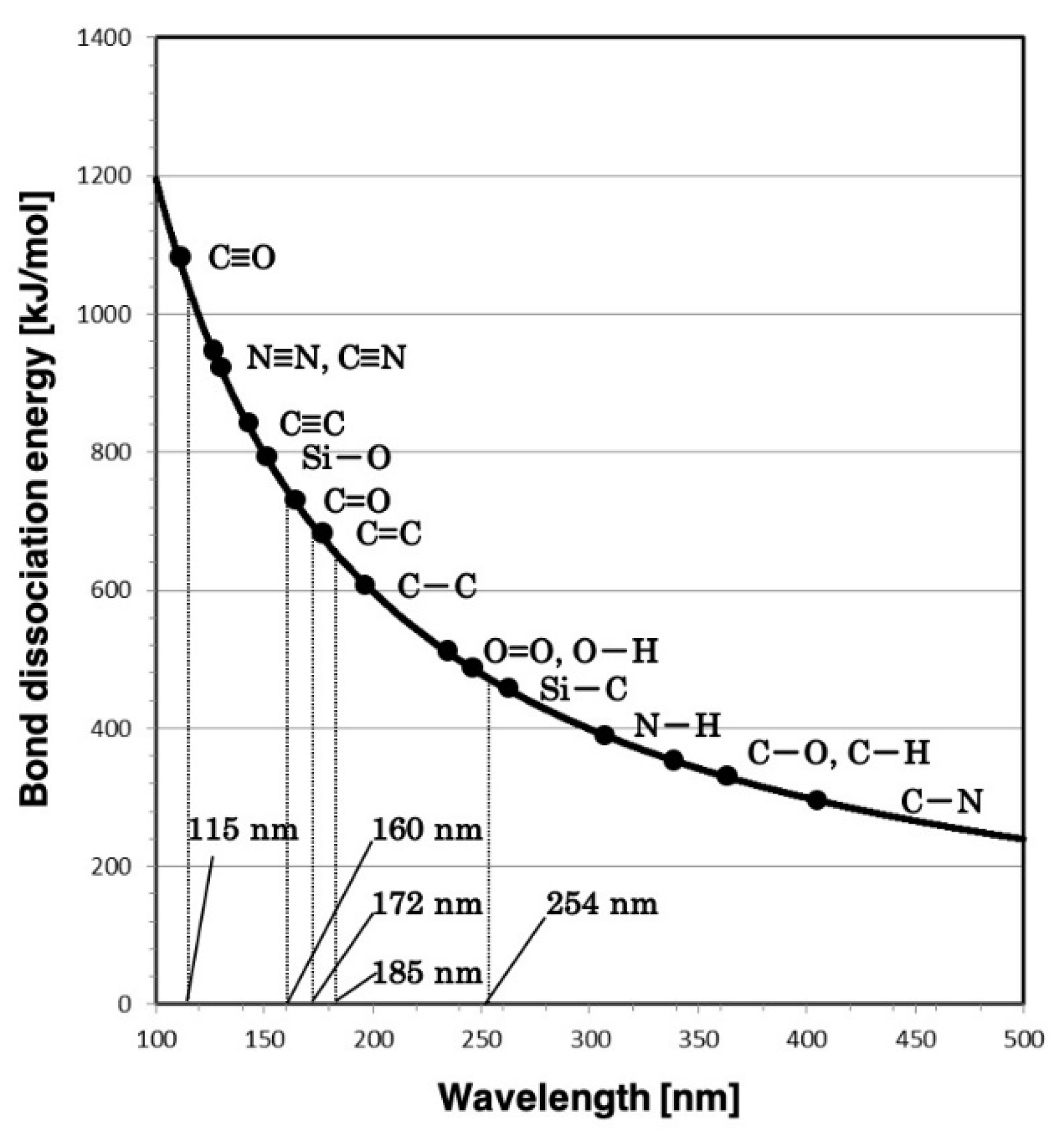
The energy of light is inversely proportional to its wavelength. VUV has a very short wavelength of between 100 nm and 200 nm, and therefore has high energy (approximately 600 to 1200 kJ/mol). Figure 1 shows the relationship between photon energy and wavelength [25,26]. The two types of light sources used in this study had peak wavelengths of 160 nm and 172 nm. The bond dissociation energy of typical molecular bonds that constitute plastic are shown, and it can be seen that single bonds such as C–C, C–O, and C–H have a lower bond dissociation energy than the photon energy associated with VUV wavelengths of 172 nm and 160 nm. The bond dissociation energy of the double bond C=O falls within the energy range associated with wavelengths of 172 nm and 160 nm. Such molecular bonds on the surface of the material can be broken by irradiating with VUV with energy higher than the bond dissociation energy [27,28,29,30].
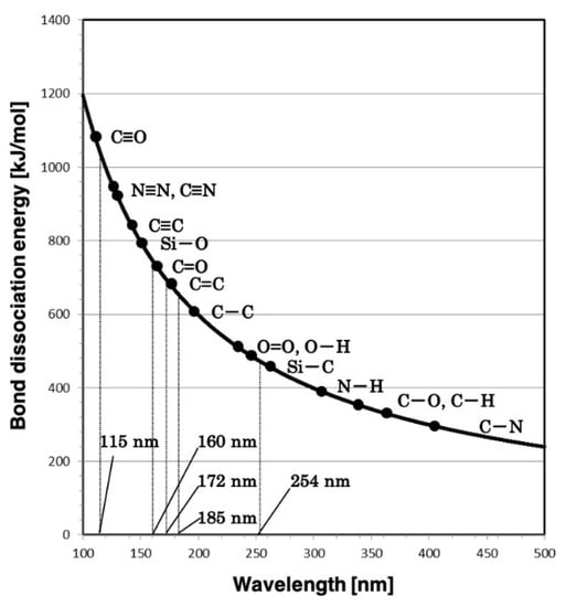
Figure 1.
Relationship between bond dissociation energy of organic molecular bonds and wavelength of photon (photon energy).
On the other hand, it is known that when the atmosphere is irradiated with VUV, oxygen molecules absorb the light energy and generate various reactive oxygen species, which can cause the molecular bonds to be broken due to oxidation by these reactive oxygen species under atmospheric conditions [23,24]. These physical effects are already being used for optical cleaning of organic stains on material surfaces [31], an optical bonding method that directly bonds plastic surfaces that are excited by VUV irradiation [32,33], and microstructure fabrication using the vitrification of silicone by irradiation with VUV [22]. In the present study, these decomposing effects of organic materials are used for etching on the plastic surface.
Two types of light sources for the VUV were used: a xenon excimer lamp with a wavelength of 172 nm (L12530-01, Hamamatsu Photonics, Hamamatsu, Japan), and a deuterium lamp with a peak wavelength of 160 nm (L12462, Hamamatsu Photonics, Hamamatsu, Japan). Although the light spectrum of the deuterium lamp ranges from 120 nm to 170 nm, since about 60% of the light output is concentrated within the wavelength of 160 ± 10 nm, it was used as a light source with a wavelength of 160 nm in this study.
A thin film (100 nm thick) of chromium patterned on synthetic quartz (1 mm thick) with high transmittance in the VUV region was used as the photomask. The amount of exposure dose was calculated from the transmittance of synthetic quartz, which is 0.85 at a wavelength of 172 nm and 0.20 at a wavelength of 160 nm, and the measured data from the exposure meter (UIT-150, USHIO INC., Tokyo, Japan). Two kinds of materials, polymethyl methacrylate (PMMA) and polycarbonate (PC) were used as etching materials, both of which have excellent light transmittance and are often used as microfluidic devices. PMMA has C=O bonds with binding dissociation energy higher than 172 nm light energy and lower than 160 nm light energy. PC also has a C=O bond, but the molecular weight of PC is higher than that of PMMA, so that the molecular weight dependency in etching can be evaluated. Therefore, PMMA and PC should be good tools for investigating the relationship between the energy of light and the bond dissociation energy.
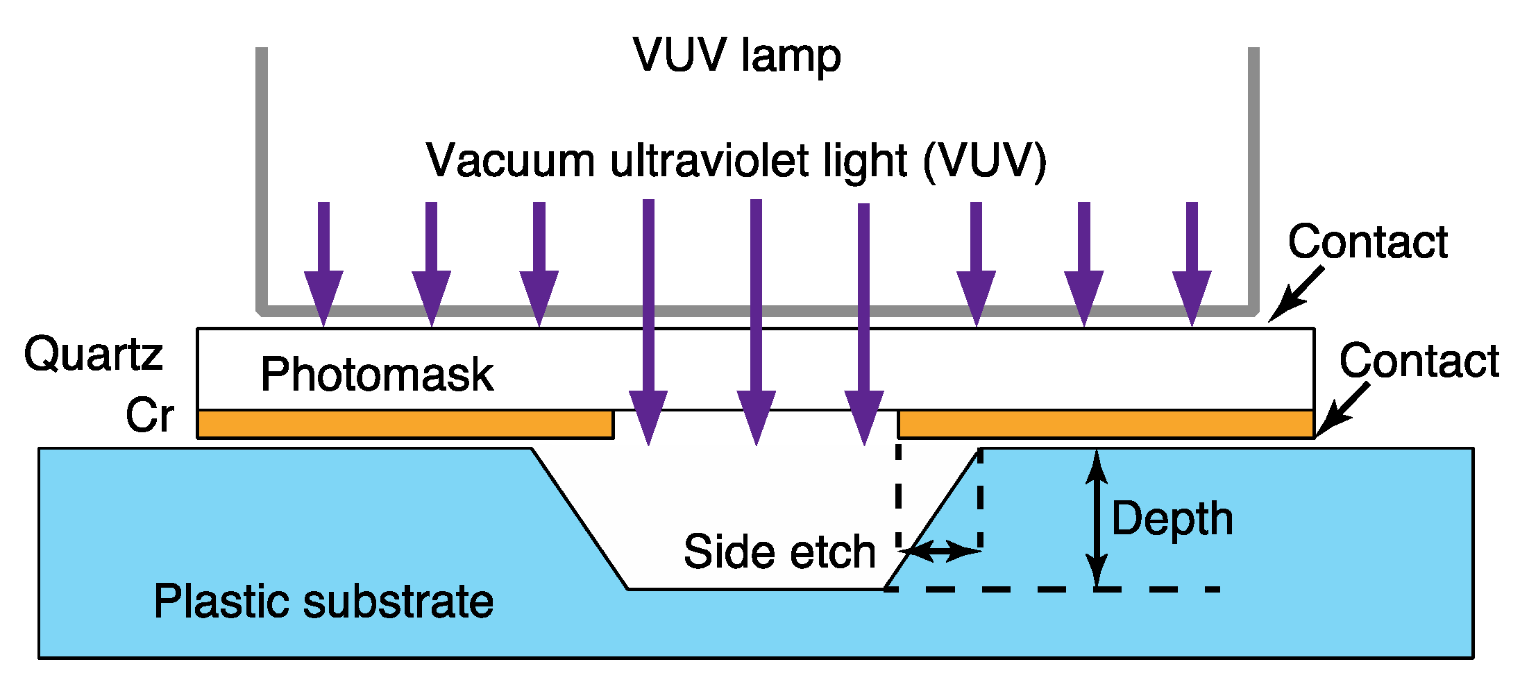
The experimental method is shown in Figure 2. We used two types of masking. One is a method using a photomask, and the other is a method for making a mask layer directly on the substrate surface. The substrate was irradiated with VUV through the photomask with the light source, the substrate and photomask in close contact in the case of using photomask. Even though the surfaces of the substrates were flat, a small gap of a few µm remained between the photomask and substrates, and it is presumed that oxygen in this gap turns into reactive oxygen species, which contributes to the etching process. On the other hand, the directly deposited mask was used, in order to investigate the effect of the small gap on patterning.
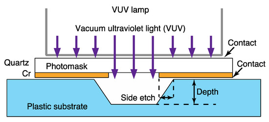
Figure 2.
Schematic of the experimental method.
The shapes of the surface of the substrate before and after processing were measured with an atomic force microscope (VN-8000, KEYENCE, Osaka, Japan), and the cross-sectional shapes after etching were evaluated to determine the etching rate of the optical etching.
3. Results
3.1. Optical Etching
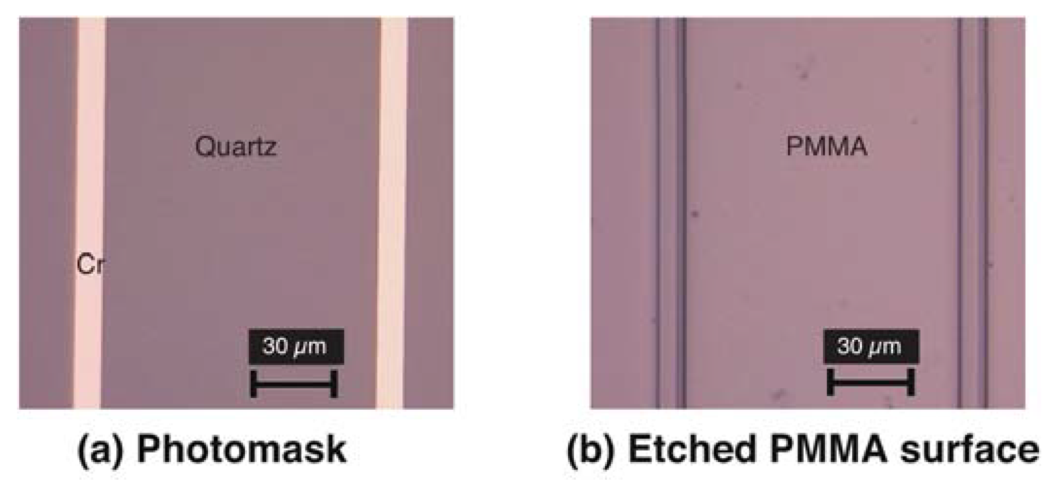
We investigated various patterns for the photomask sizing from several hundred µm to 500 nm. Figure 3a shows the typical design used as the photomask with line and space patterns of 10 µm and 100 µm respectively. Figure 3b is a magnified photograph of the surface of the PMMA substrate after being exposed to 800 mJ of VUV with a wavelength of 160 nm. The patterns from the photomask can be clearly seen to have been transferred to the PMMA substrate by VUV irradiation.
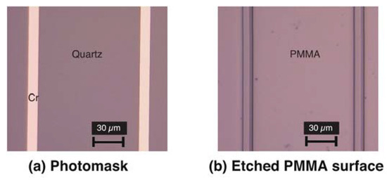
Figure 3.
Typical result of optical etching, (a) magnified photograph of the photomask, (b) etched surface on polymethyl methacrylate (PMMA).
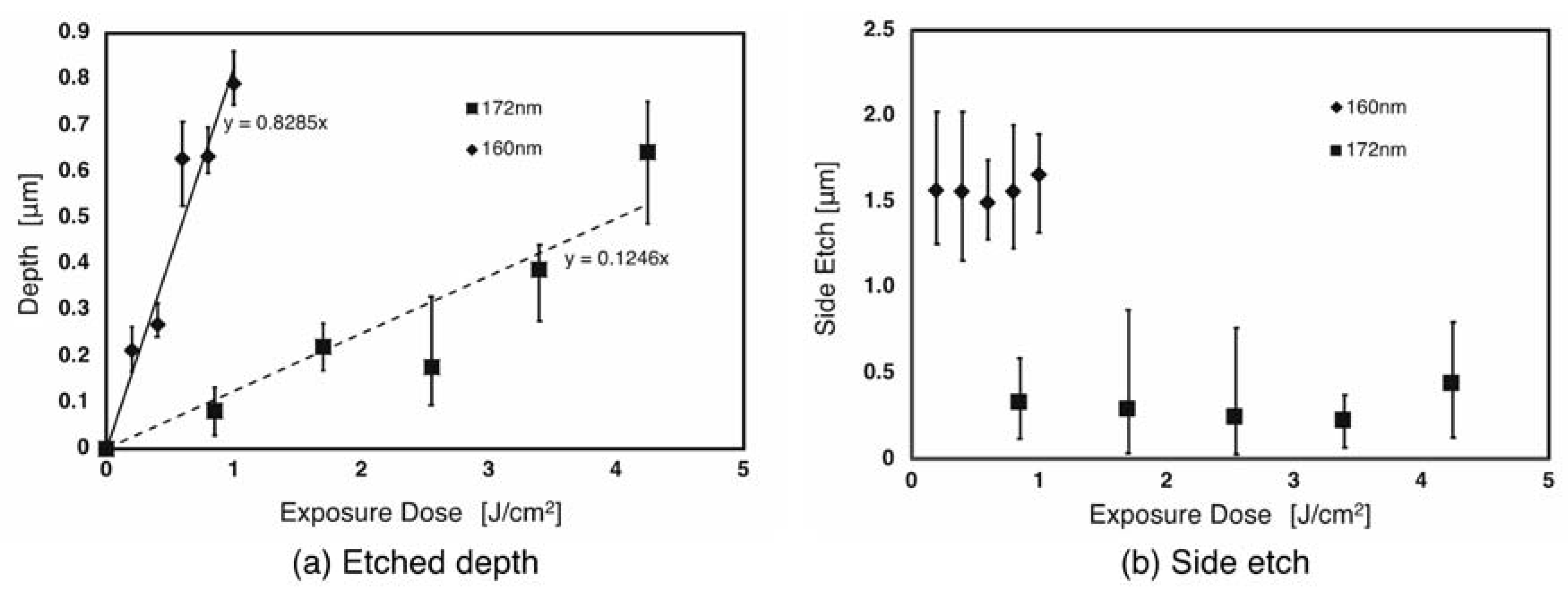
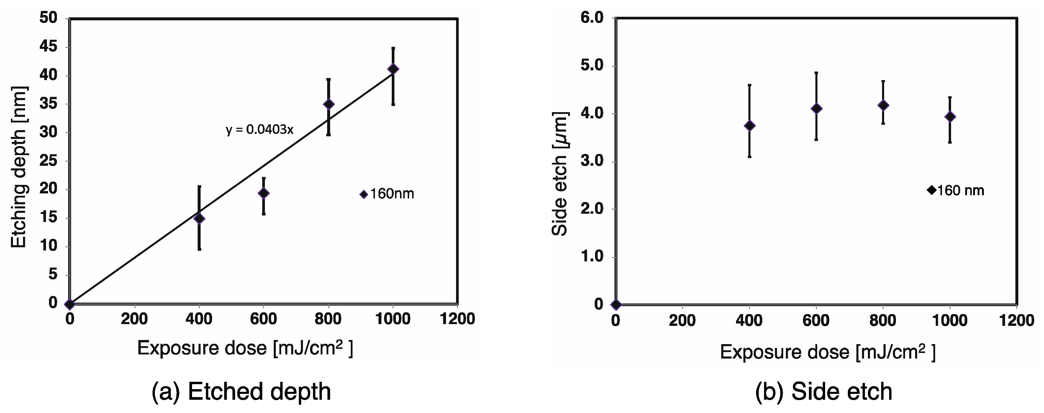
The atomic force microscope measurements of the etching depth and the side etching length are shown in Figure 4. The exposure dose and etching depth are seen to have a linear relationship for both PMMA and PC. Figure 4 shows that the average etching rate for PMMA was 0.12 µm/J at a wavelength of 172 nm and 0.83 µm/J at a wavelength of 160 nm (Figure 4a). The side etching length however, despite some variation, was found to be fairly constant regardless of the exposure dose, being about 0.5 to 1.0 µm at a wavelength of 172 nm and about 1.2 to 1.8 µm at a wavelength of 160 nm (Figure 4b). Figure 5 shows the same measurements for PC at a wavelength of 160 nm only, as etching could not be confirmed at a wavelength of 172 nm. The etching rate was 0.03 nm/J, which is lower than that of PMMA as shown in Figure 5a. The side etching length was again fairly constant regardless of the exposure dose at between 3 and 4.5 µm as shown in Figure 5b.
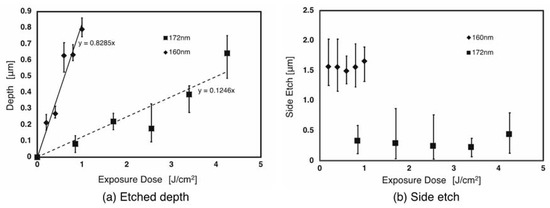
Figure 4.
Results of optical etching of PMMA, (a) etched depth and (b) side etching.
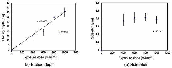
Figure 5.
Results of optical etching of PC, (a) etched depth and (b) side etching.
3.2. Fabrication of Microfluidic Device by Optical Etching and Bonding
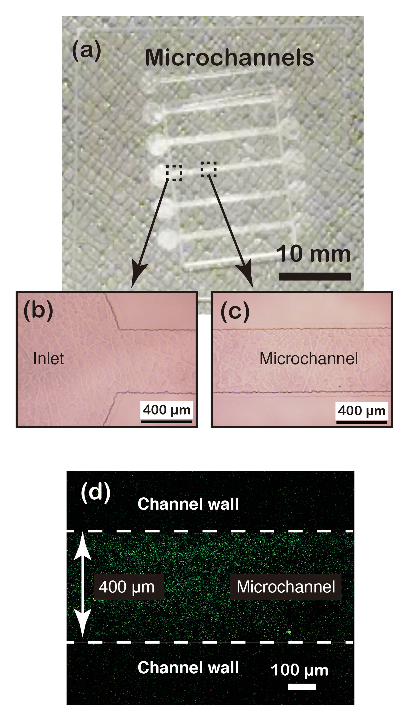
We made a prototype of a PMMA made microfluidic device using only VUV irradiation. The results of the present study show that plastic etching is possible with VUV, and our previous research shows that plastic surfaces can be directly bonded by mere exposure to VUV (optical bonding method) [20,21]. We therefore tried to demonstrate that plastic-made microfluidic devices can be fabricated with VUV, through a combination of optical bonding and optical etching methods. The PMMA surface was exposed to 3 J/cm2 of VUV at a wavelength of 160 nm through a photomask with a channel pattern. Figure 6a–c show the resulting channel structures with a depth of about 3 µm fabricated on the substrate. VUV irradiation at 60 mJ/cm2 and a wavelength of 160 nm on the bonding surface of the channel substrate, and on the surface of another PMMA substrate, enabled the two substrates to be bonded together to create a closed microchannel device. A pressure of 5.0 MPa was applied during bonding to ensure contact between the substrates.
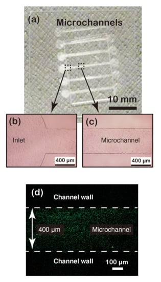
Figure 6.
Fabrication of microfluidic device by optical etching and bonding: (a) fabricated microchannels, (b) magnified view of the inlet part, (c) magnified view of channel part, and (d) fluorescent particles flowing inside the microchannel.
The bonding efficacy of the fabricated device was evaluated by feeding a solution into the microchannel, containing fluorescent particles (S1392, Invitrogen) at the concentration of 1011 particle/mL, the results of which are shown in Figure 6d. The figure shows that the fluorescent particles are only present in the channel portion, confirming that the surfaces are sealed uniformly.
4. Discussion
The etching depth of PMMA was deeper at a wavelength of 160 nm than at 172 nm. When organic materials were irradiated with VUV at a wavelength of 172 nm, a reduction in methyl groups was observed [19,24]. Similarly, when organic materials were irradiated with VUV at a wavelength of 160 nm, not only was there a reduction in methyl groups but also a decrease in C=O bonds [21], which is greater than the energy of VUV at a wavelength of 172 nm but lower than the energy at 160 nm. Moreover, the absorptivity of PMMA at 160 nm was found to be more than double that at 172 nm [21]. It is not quite clear why the etching rate of PC should be lower than that of PMMA; however, the difference in etching rates for the two wavelengths may be attributed to these effects.
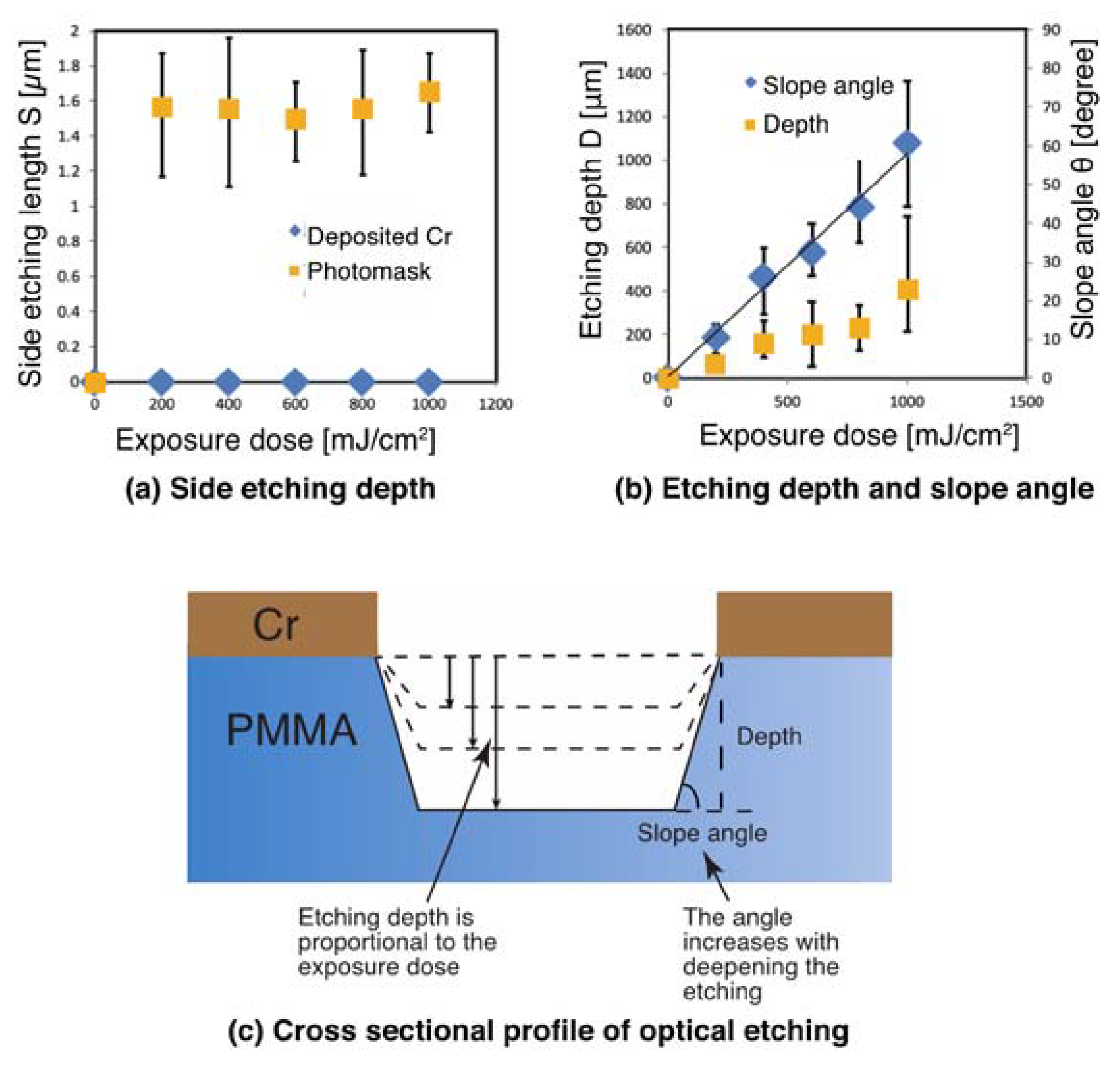
The side etching length was fairly constant in both PMMA and PC, irrespective of the etching depth. The reason that the side etch length was greater than the etching depth could be due to poor contact between the photomask and substrate because of the unevenness of the substrate surface. To confirm this, optical etching was conducted by directly depositing and patterning a Cr layer on the PMMA substrate by vacuum deposition using a stencil mask. This meant that the optical etching was done by ensuring no gaps between the photomask and the substrate surface during exposure. The results in Figure 7a and b show that there are no discernible side etchings detected. The side etching seen in Figure 4 and Figure 5 is believed to be caused by light intrusion due to poor contact between the photomask and substrate. As shown in Figure 7b, the slope angle increases with exposure dose and resulting etching depth, indicating that the etching proceeds as shown in Figure 7c. These results suggest that deep etching with a high aspect ratio may be possible depending on the exposure dose.
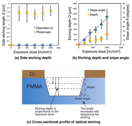
Figure 7.
Optical etching (a) side etching difference between photomask and deposited Cr, (b) etching rate versus slope angle, (c) schematic of the etched cross-sectional profile.
5. Conclusions
In this study, a VUV at two different wavelengths was used to demonstrate an optical etching method that is suitable for mass production on account of its simple process and large area of exposure. In the case of VUV at a wavelength of 160 nm, the etching was successful on both PMMA and PC, although there were differences in etching rates. It was also found that the etching depth is proportional to the exposure dose and that the etching is anisotropic. Etching by irradiation at a wavelength of 172 nm was possible on PMMA but not on PC. It was deduced that the optical etching success dependence on wavelength is due to factors such as the bond dissociation energy of the molecular bonds that make up the material, and the photon energy (directly related to the wavelength), so further work will be done to study these relationships in more detail. Future studies will also include research into the role of photon energy and reactive oxygen species in the etching process.
Furthermore, by combining the optical etching method proposed in this study with the optical bonding method established in our previous research, we succeeded in developing a new method to fabricate devices using only VUV irradiation through the example of fabricating a microfluidic device.
In addition to organic structural materials, this method will be used to develop the patterning of functional organic materials such as organic electronic materials in the future, as well as developing a new microfabrication method for organic microdevices using light.
Author Contributions
Investigation, T.D.; supervision, methodology, project administration, resources, writing—original draft, and writing—review and editing, T.Y. All authors have read and agreed to the published version of the manuscript.
Funding
This work was supported by a Grant-in-Aid for Scientific Research (KAKENHI) (No. 17H03246, 20H02160) from the Japan Society for the Promotion of Science (JSPS).
Conflicts of Interest
The authors declare no conflict of interest.
References
- Chou, W.L.; Lee, P.Y.; Yang, C.L.; Huang, W.Y.; Lin, Y.S. Recent advances in applications of droplet microfluidics. Micromachines 2015, 6, 1249–1271. [Google Scholar] [CrossRef]
- Liu, Z.; Han, X.; Qin, L. Recent progress of microfluidics in translational applications. Adv. Healthc. Mater. 2016, 5, 871–888. [Google Scholar] [CrossRef]
- Gao, D.; Jin, F.; Zhou, M.; Jiang, Y. Recent advances in single cell manipulation and biochemical analysis on microfluidics. Analyst 2019, 144, 766–781. [Google Scholar] [CrossRef] [PubMed]
- Song, Y.; Lin, B.; Tian, T.; Xu, X.; Wang, W.; Ruan, Q.; Guo, J.; Zhu, Z.; Yang, C. Recent progress in microfluidics-based biosensing. Anal. Chem. 2018, 91, 388–404. [Google Scholar] [CrossRef] [PubMed]
- Miled, A.; Greener, J. Recent advancements towards full-system microfluidics. Sensors 2017, 17, 1707. [Google Scholar] [CrossRef] [PubMed]
- Brince, P.K.; Panigrahi, A.K.; Singh, V.; Singh, S.G. Nonlithographic fabrication of plastic-based nanofibers integrated microfluidic biochip for sensitive detection of infectious biomarker. ACS Appl. Mater. Interfaces 2017, 9, 39994–40005. [Google Scholar]
- Chandrasekaran, A.; Kalashnikov, N.; Rayes, R.; Wang, C.; Spicer, J.; Moraes, C. Thermal scribing to prototype plastic microfluidic devices, applied to study the formation of neutrophil extracellular traps. Lab Chip 2017, 17, 2003–2012. [Google Scholar] [CrossRef] [PubMed]
- Klammer, I.; Hofmann, M.C.; Buchenauer, A.; Mokwa, W.; Schnakenberg, U. Long-term stability of PDMS-based microfluidic systems used for biocatalytic reactions. J. Micromech. Microeng. 2006, 16, 2425. [Google Scholar] [CrossRef]
- Adamiak, W.; Kałuża, D.; Jönsson-Niedziolka, M. Compatibility of organic solvents for electrochemical measurements in PDMS-based microfluidic devices. Microfluid. Nanofluid. 2016, 20, 127. [Google Scholar] [CrossRef]
- Guckenberger, D.J.; de Groot, T.E.; Wan, A.M.D.; Beebe, D.J.; Young, E.W.K. Micromilling: A method for ultra-rapid prototyping of plastic microfluidic devices. Lab Chip 2015, 15, 2364–2378. [Google Scholar] [CrossRef]
- Iwai, K.; Shih, K.C.; Lin, X.; Brubaker, T.A.; Sochol, R.D.; Lin, L. Finger-powered microfluidic systems using multilayer soft lithography and injection molding processes. Lab Chip 2014, 14, 3790–3799. [Google Scholar] [CrossRef] [PubMed]
- Mair, D.A.; Geiger, E.; Pisano, A.P.; Fréchet, J.M.J.; Svec, F. Injection molded microfluidic chips featuring integrated interconnects. Lab Chip 2006, 6, 1346–1354. [Google Scholar] [CrossRef] [PubMed]
- Xia, Y.; McClelland, J.J.; Gupta, R.; Qin, D.; Zhao, X.M.; Sohn, L.L.; Celotta, R.J.; Whitesides, G.M. Replica molding using polymeric materials: A practical step toward nanomanufacturing. Adv. Mater. 1997, 9, 147–149. [Google Scholar] [CrossRef]
- Fiorini, G.S.; Jeffries, G.D.M.; Lim, D.S.W.; Kuyper, C.L.; Chiu, D.T. Fabrication of thermoset polyester microfluidic devices and embossing masters using rapid prototyped polydimethylsiloxane molds. Lab Chip 2003, 3, 158–163. [Google Scholar] [CrossRef] [PubMed]
- Chiang, Y.M.; Bachman, M.; Chu, C.; Li, G.P. Characterizing the Process of cast molding microfluidic systems. In Microfluidic Devices and Systems II, Proceedings of the Symposium on Micromachining and Microfabrication, Santa Clara, CA, US, 19 August 1999; International Society for Optics and Photonics: Bellingham, WA, USA, 1999; Volume 3877, pp. 303–311. [Google Scholar]
- Bhattacharjee, N.; Urrios, A.; Kang, S.; Folch, A. The upcoming 3D-printing revolution in microfluidics. Lab Chip 2016, 16, 1720–1742. [Google Scholar] [CrossRef] [PubMed]
- Ho, C.M.B.; Ng, S.H.; Li, K.H.H.; Yoon, Y.J. 3D printed microfluidics for biological applications. Lab Chip 2015, 15, 3627–3637. [Google Scholar] [CrossRef]
- Chen, J.; Zhou, Y.; Wang, D.; He, F.; Rotello, V.M.; Carter, K.R.; Watkins, J.J.; Nugen, S.R. UV-nanoimprint lithography as a tool to develop flexible microfluidic devices for electrochemical detection. Lab Chip 2015, 15, 3086–3094. [Google Scholar] [CrossRef]
- Lin, T.Y.; Do, T.; Kwon, P.; Lillehoj, P.B. 3D printed metal molds for hot embossing plastic microfluidic devices. Lab Chip 2017, 17, 241–247. [Google Scholar] [CrossRef]
- Nilsson, D.; Balslev, S.; Kristensen, A. microfluidic dye laser fabricated by nanoimprint lithography in a highly transparent and chemically resistant cyclo-olefin copolymer (COC). J. Micromech. Microeng. 2005, 15, 296. [Google Scholar] [CrossRef]
- Horsley, D.A.; Talin, A.A.; Skinner, J.L. Micromechanical and microfluidic devices incorporating resonant metallic gratings fabricated using nanoimprint lithography. J. Nanophoton. 2008, 2, 021785. [Google Scholar]
- Hashimoto, Y.; Yamamoto, T. Fabrication of an anti-reflective and super-hydrophobic structure by vacuum ultraviolet light-assisted bonding and nanoscale pattern transfer. Micromachine 2018, 9, 186. [Google Scholar] [CrossRef] [PubMed]
- Hashimoto, Y.; Matsuzawa, S.; Yamamoto, T. Subsurface investigation of the surface modification of polydimethylsiloxane by 172-nm vacuum ultraviolet irradiation using ToF-SIMS and VUV spectrometry. Surf. Interface Anal. 2018, 50, 752–756. [Google Scholar] [CrossRef]
- Hashimoto, Y.; Yamamoto, T. Solid state direct bonding of polymers by vacuum ultraviolet light below 160 nm. Appl. Surf. Sci. 2017, 419, 319–327. [Google Scholar] [CrossRef]
- Cottrell, T.L. The Strengths of Chemical Bonds, 2nd ed.; Butterworths Publications Ltd.: London, UK, 1958. [Google Scholar]
- Darwent, B.B. Bond Dissociation Energiese in Simple Molecules; National Standard Reference Data Series. In National Bureau of Standards; United States Department of Commerce: Washington, DC, USA, 1970; Volume 31.
- Fouchier, M.; Pargon, E.; Azarnouche, L.; Menguelti, K.; Joubert, O.; Cardolaccia, T.; Bae, Y.C. Vacuum ultra violet absorption spectroscopy of 193 nm photoresists. Appl. Phys. A 2011, 105, 399–405. [Google Scholar] [CrossRef]
- Kogelschatz, U. Dielectric-Barrier discharges: Their history, discharge physics, and industrial applications. Plasma Chem. Plasma Process. 2003, 23, 1–46. [Google Scholar] [CrossRef]
- Graubner, V.M.; Jordan, R.; Nuyken, O.; Schnyder, B.; Lippert, T.; Kotz, R.; Wokaun, A. Photochemical modification of cross-linked poly(dimethylsiloxane) by irradiation at 172 nm. Macromolecules 2004, 37, 5936–5943. [Google Scholar] [CrossRef]
- Holländer, A.; Behnisc, J. Vacuum-ultraviolet photolysis of polymers. Surf. Coat. Technol. 1998, 98, 855–858. [Google Scholar] [CrossRef]
- Strein, E.L.; Allred, D. Eliminating carbon contamination on oxidized Si surfaces using a VUV excimer lamp. Thin Solid Films 2008, 517, 1011–1015. [Google Scholar] [CrossRef]
- Yamamoto, T. Study on 172-nm vacuum ultraviolet light surface modifications of polydimethylsiloxane for micro/nanofluidic applications. Surf. Interface Anal. 2010, 43, 1271–1276. [Google Scholar] [CrossRef]
- Hashimoto, Y.; Mogi, K.; Yamamoto, T. Vacuum ultraviolet light assisted bonding and nanoscale pattern transfer method for polydimethylsiloxane. Microelectron. Eng. 2017, 176, 116–120. [Google Scholar] [CrossRef]
© 2020 by the authors. Licensee MDPI, Basel, Switzerland. This article is an open access article distributed under the terms and conditions of the Creative Commons Attribution (CC BY) license (http://creativecommons.org/licenses/by/4.0/).

