Organic Thin-Film Transistors as Gas Sensors: A Review

 ,
,  ,
,  ,
,  , , , and
Abstract
:
1. Introduction

2. Organic Thin-Film Transistors
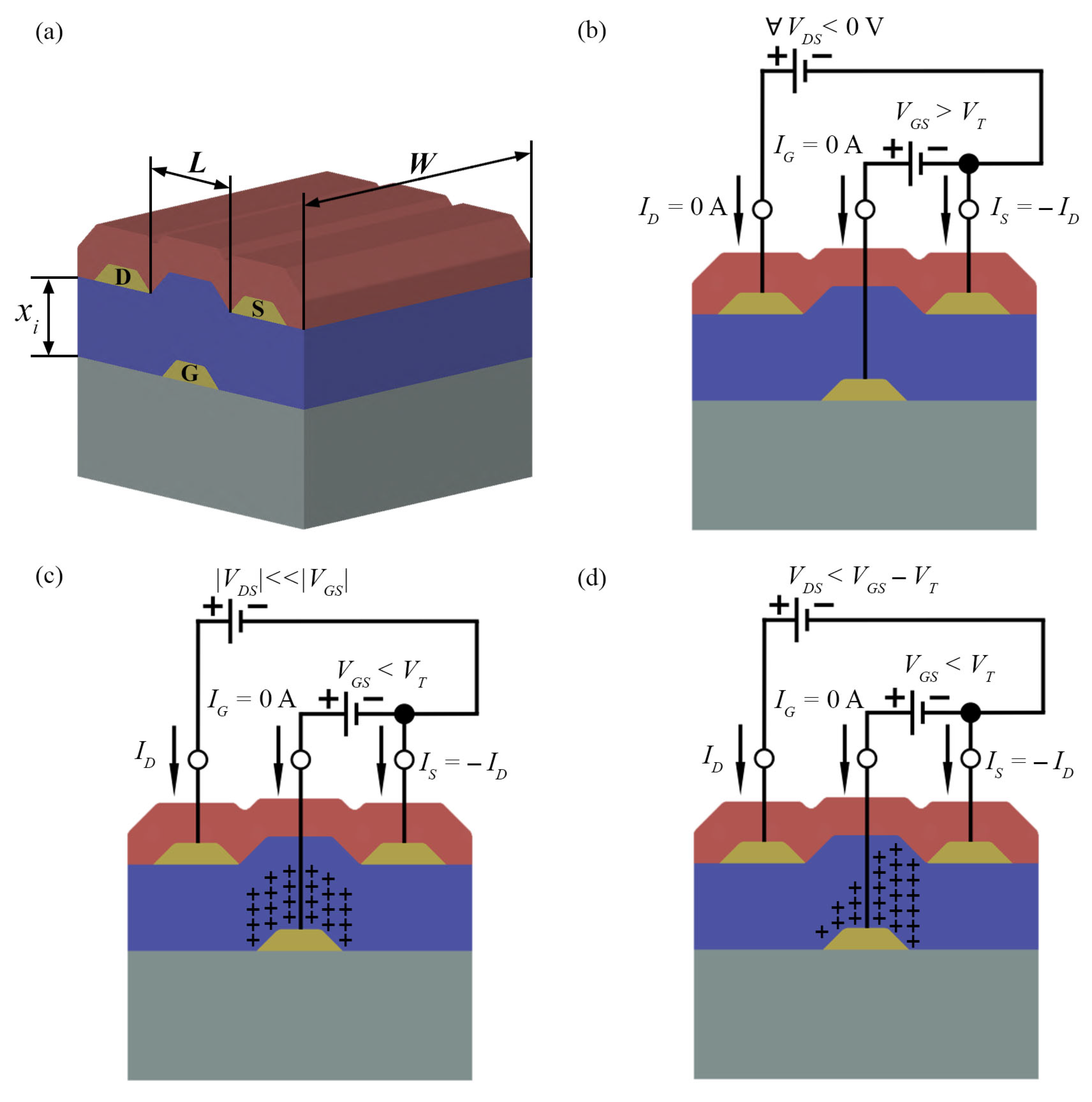
2.1. Operating Principles
2.2. Characteristic Parameters
2.2.1. Charge Carrier Mobility
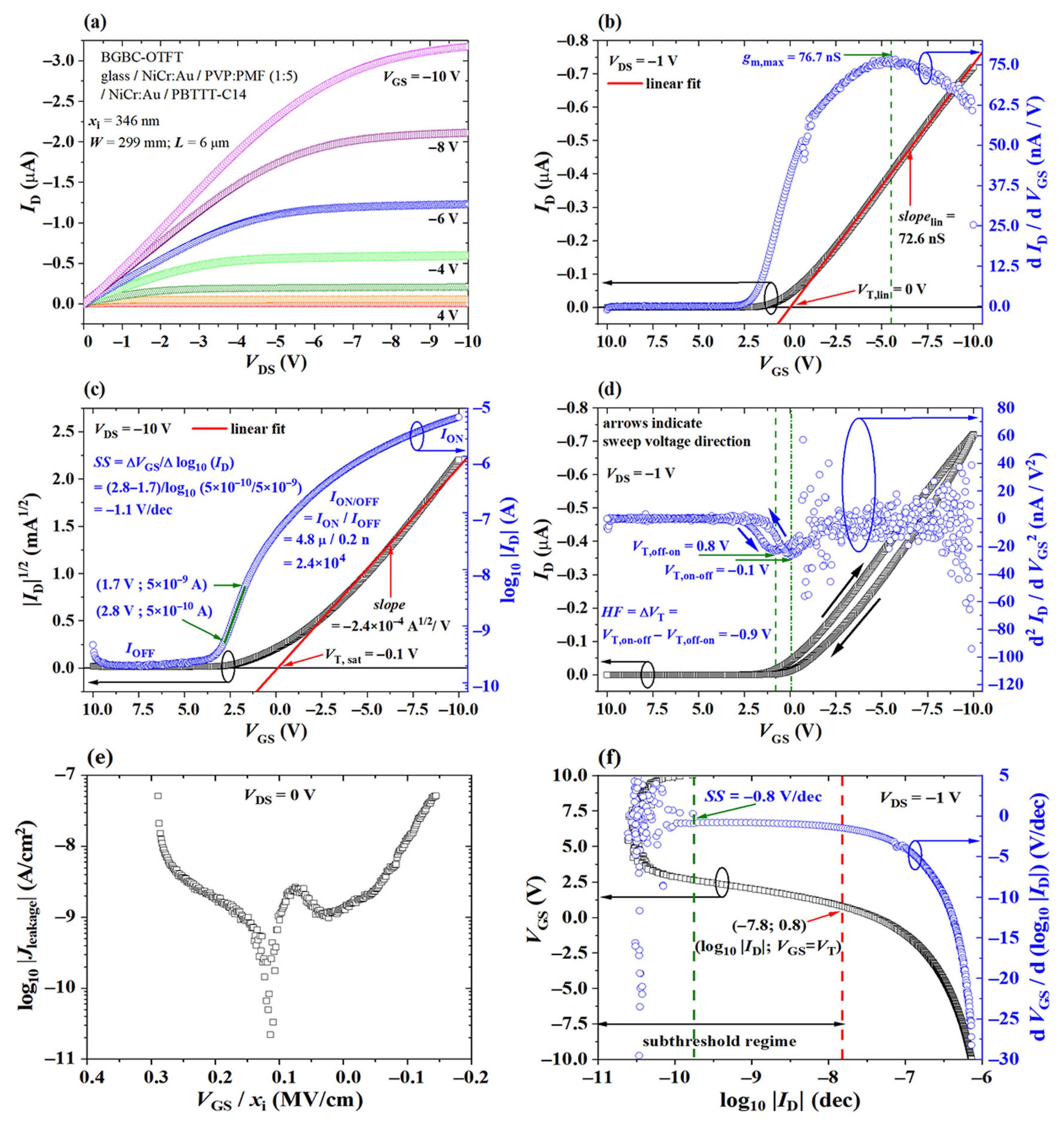
2.2.2. Threshold Voltage
2.2.3. Current On/Off Ratio
2.2.4. Subthreshold Slope
2.2.5. Gas Sensing Response
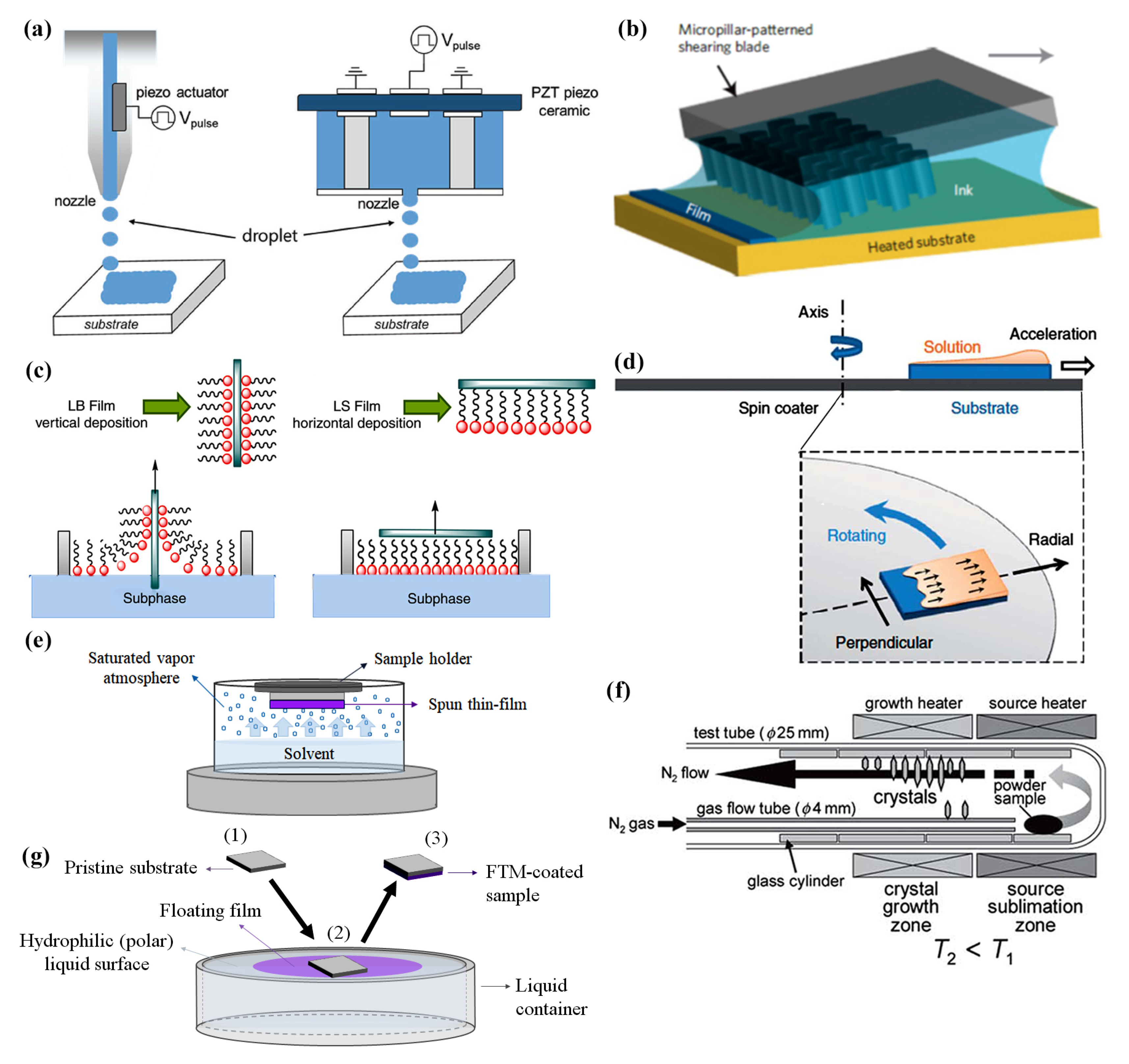
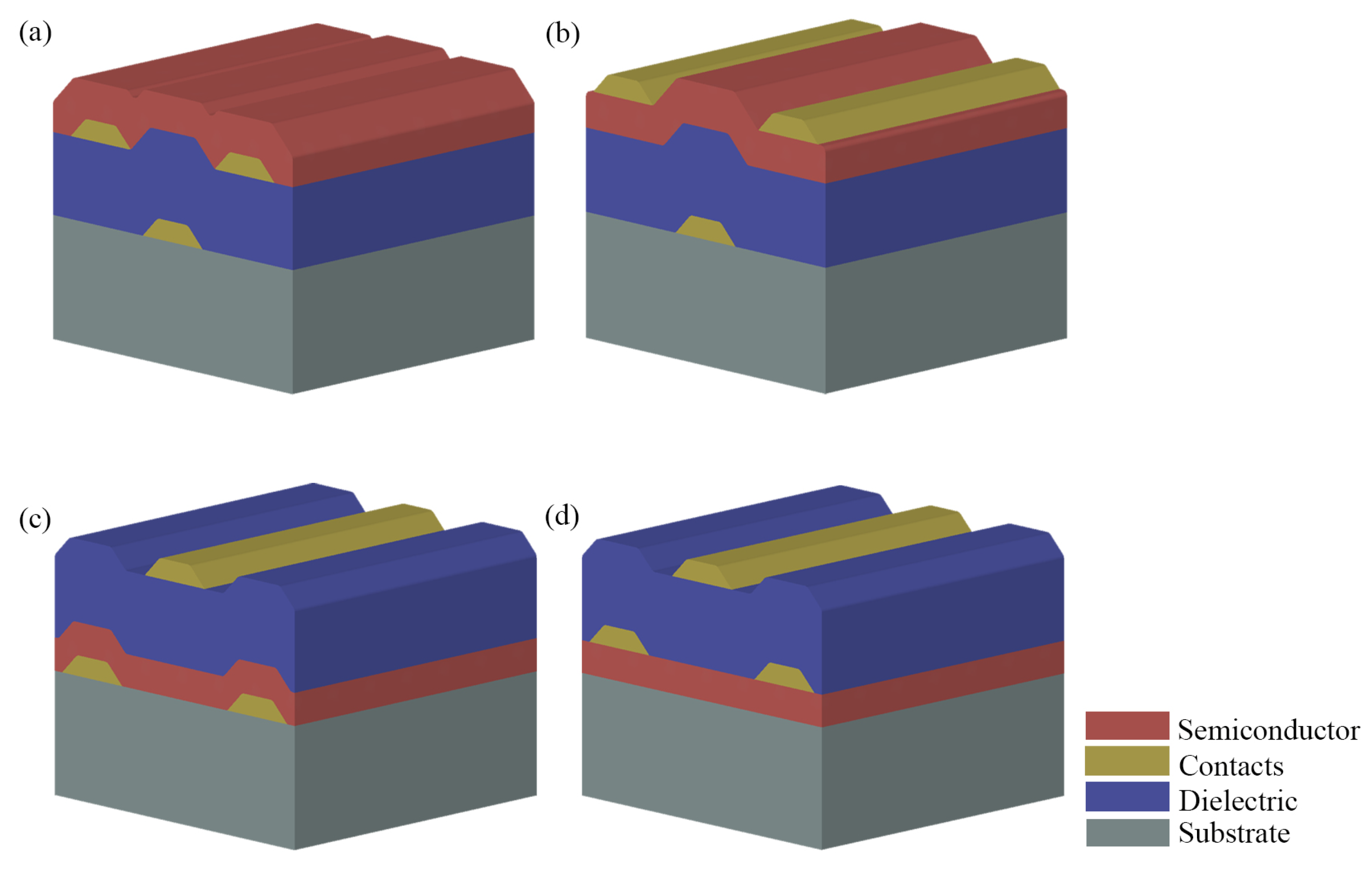
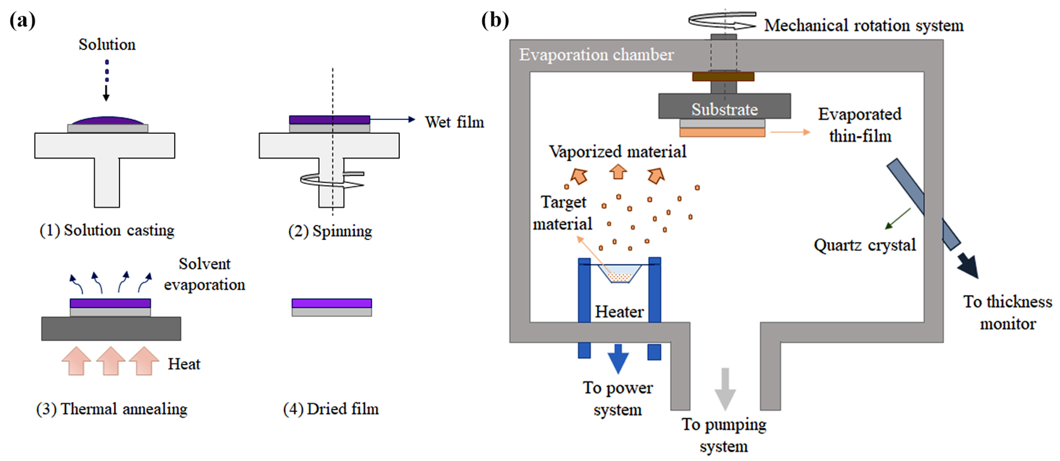
2.3. Fabrication Techniques
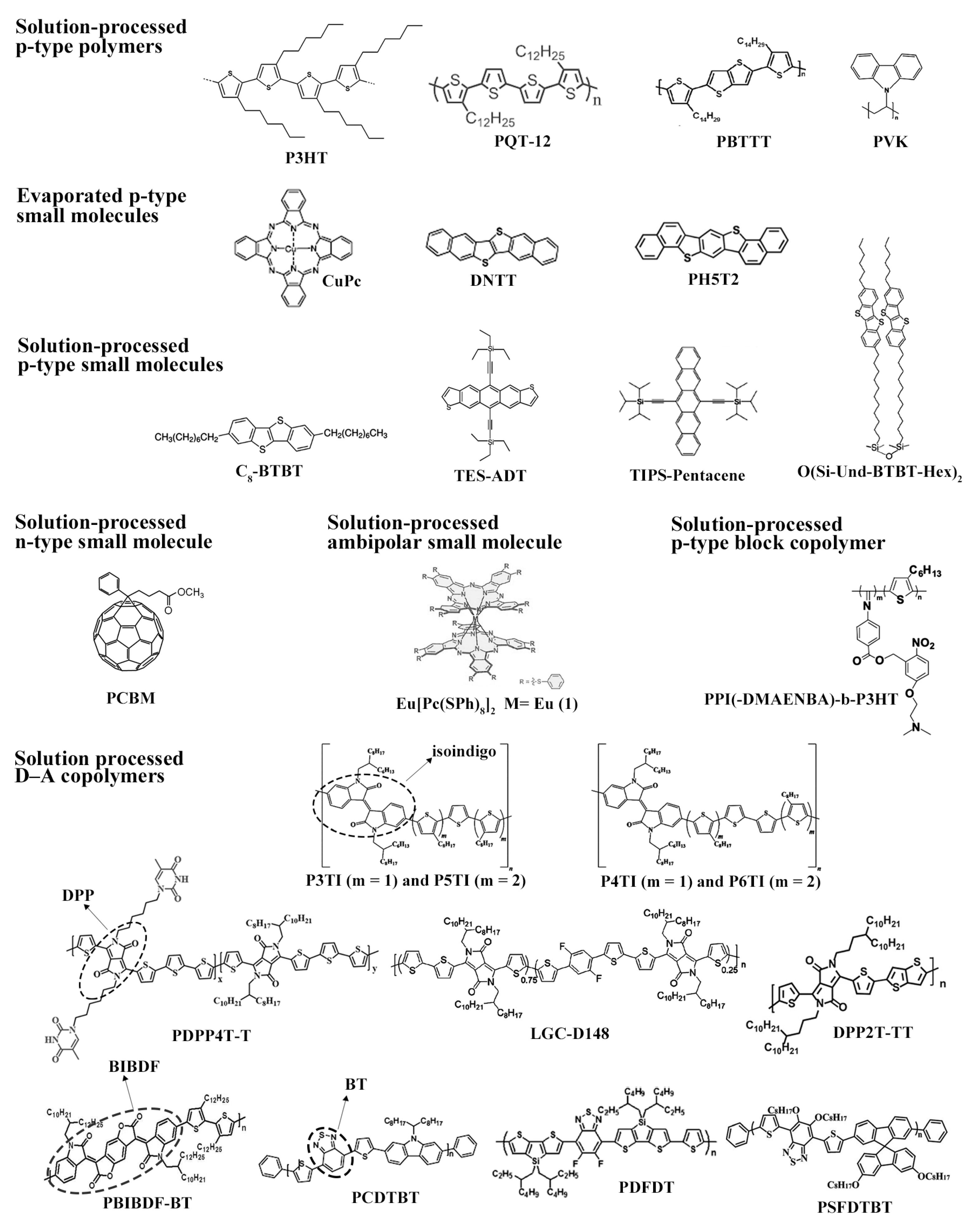
2.4. Organic Materials
2.5. Gas Sensing Applications
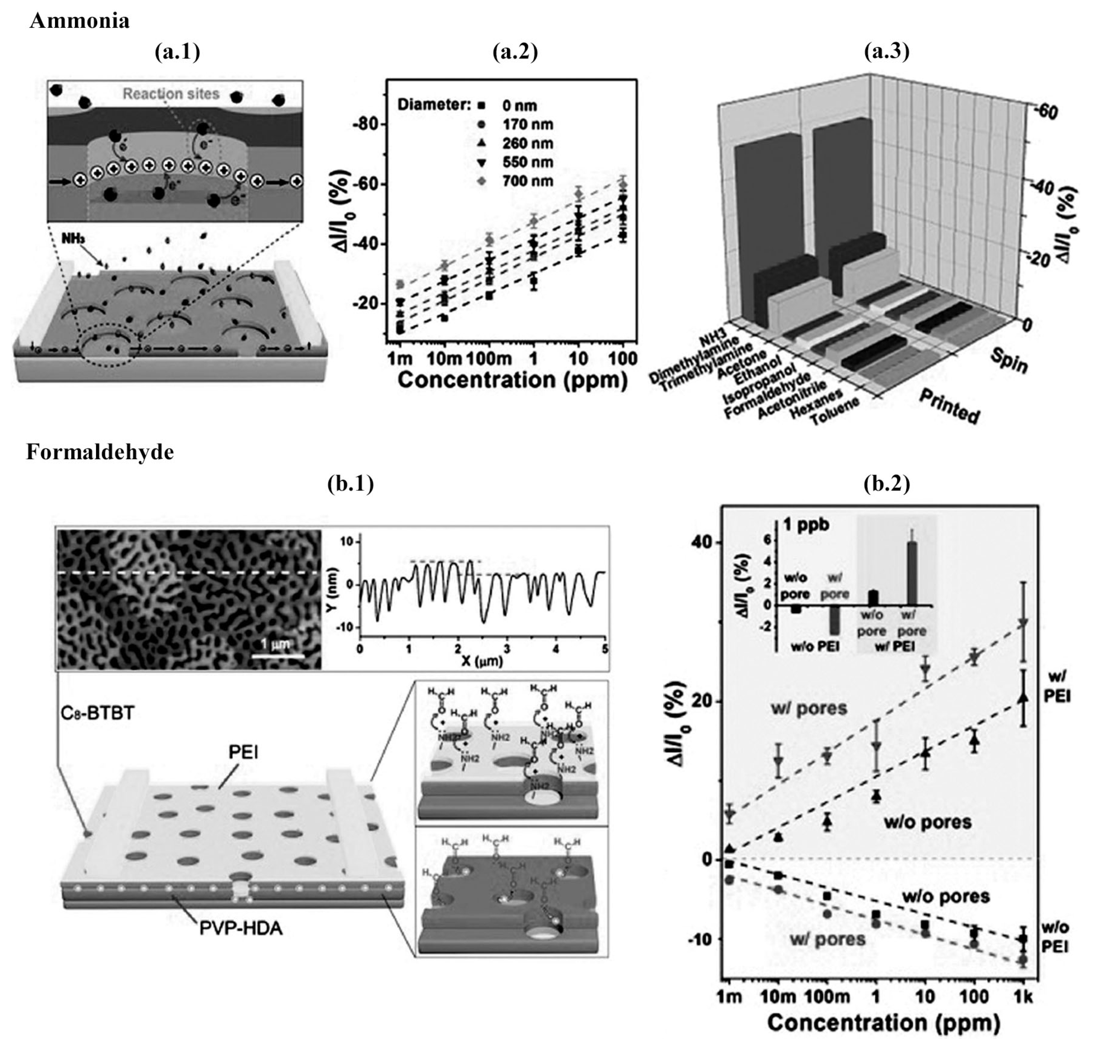
2.5.1. NH
2.5.2. VOCs

| Analyte | Semiconductor | Technique | Structure ‡ | R (%) | (s) | V (V) | Selective | Year | Ref. | |
|---|---|---|---|---|---|---|---|---|---|---|
| Acetone | P3HT | spin coating | BGBC | 440 ppm | 1.5 @ 244 ppm () | 68 | No | 2015 | [70] | |
| Chloroform | P3HT | spin coating | BGBC | 1100 ppm | 6 @ 222 ppm () | 201 | No | 2015 | [70] | |
| Ethanol | P3HT (porous) | spin coating | BGTC | 100 ppm | 33.7 @ 1000 ppm () | - | Yes | 2019 | [73] | |
| Ethylene | P3HT:Pd (porous) | spin coating | BGBC | 25 ppm | 30.2 @ 25 ppm () | 300 | Yes | 2017 | [90] | |
| Formaldehyde | C-BTBT | off-center spinning | BGTC | 1 ppb | 5.8 @ 1 ppb () | 2 | Yes | 2017 | [85] | |
| Methanol | P3HT | spin coating | BGBC | 570 ppm | 3.5 @ 443 ppm () | 161 | No | 2015 | [70] | |
| NH | P3HT | spin coating | BGBC | 1 ppm | 25 @ 67 ppm () | 52 | Yes | 2015 | [70] | |
| P3HT:PS | spin coating | BGTC | 5 ppm | 52 @ 5 ppm () | - | Yes | 2016 | [98] | ||
| P3HT | LB-nTM | BGTC | 8 ppb | 68.8 @ 1 ppm () | - | Yes | 2017 | [80] | ||
| P3HT (NW) | spin coating | BGBC | 20 ppm | 24.2 @ 20 ppm () | - | Yes | 2018 | [81] | ||
| P3HT (porous) | spin coating | BGTC | 1 ppm | 17.7 @ 10 ppm () | - | Yes | 2019 | [73] | ||
| PQT-12:CdSe | FTM | BGTC | 20 ppm | 12.5 @ 20 ppm () | 65 | No | 2018 | [87] | ||
| PBTTT | FTM | BGTC | 330 ppb | 12.52 @ 1 ppm (I) | 26 | Yes | 2017 | [84] | ||
| DNTT (porous) | evaporation | BGTC | 10 ppb | 73 @ 1 ppm () | 95 | Yes | 2017 | [83] | ||
| Eu[Pc(SPh)] | quasi-LS | BGTC | 15 ppm | 14 @ 800 ppm () | 120 | 50 | Yes | 2018 | [86] | |
| O(Si-Und-BTBT-Hex) | LS | BGBC | 50 ppb | 37.5 @ 1 ppm () | 180 | Yes | 2018 | [72] | ||
| PPI(-DMAENBA)-b-P3HT | spin coating | BGTC | 10 ppb | 28.6 @ 100 ppb () | 3–7 | No | 2018 | [82] | ||
| PnTI | spin coating | BGTC | 1 ppm | 10–20 ppm () | 60–180 | No | 2018 | [88] | ||
| LGC-D148 | spin coating | TGBC | 1000 ppm | 98.3 @ 1000 ppm () | - | No | 2017 | [99] | ||
| DPP2T-TT (porous) | blade coating | BGTC | 1 ppb | 27.8 @ 1 ppb () | 1 | Yes | 2017 | [85] | ||
| PDFDT | blade coating | BGTC | 1 ppm | 56.4 @ 10 ppm () | 180 | No | 2017 | [100] | ||
| NO | P3HT:ZnO@GO | spin coating | BGTC | 1 ppm | 32 @ 1 ppm () | 300 | No | 2017 | [94] | |
| P3HT:PVK | spin coating | BGTC | 139.3 ppb | 687 @ 600 ppb () § | 300 | Yes | 2018 | [105] | ||
| P3HT | spray coating | BGBC | 10 ppm | 320 @ 10 ppm () | 500 | Yes | 2018 | [106] | ||
| CuPc | evaporation | BGTC | 415 ppb | 160,000 @ 5 ppm () | 600 | Yes | 2017 | [107] | ||
| CuPc (NW)/Ph5T2 | evaporation | BGTC | 50 ppb | 424 @ 10 ppm () | 1080 | Yes | 2017 | [92] | ||
| Pentacene | evaporation | BGBC | 1 ppm | 22.7 @ 30 ppm () | 180 | No | 2017 | [103] | ||
| TES-ADT | spin coating/SVA | BGTC | 10 ppm | 23.8 @ 30 ppm (I) | 20 | No | 2018 | [97] | ||
| TIPS-pentacene | spin coating | BGTC | 200 ppb | 539 @ 1 ppm () | 800 | Yes | 2018 | [101] | ||
| TIPS-pentacene:PS | spin coating/SD | BGTC | 1 ppm | 8 @ 50 ppm () | 50 | No | 2019 | [95] | ||
| TIPS-pentacene | off-center spinning | BGTC | 1 ppm | 44.3 @ 250 ppb () | 800 | Yes | 2019 | [102] | ||
| TIPS-pentacene | spin coating | BGTC | 1.93 ppb | 1329 @ 1 ppm () § | 500 | Yes | 2019 | [96] | ||
| PCDTBT † | spin coating | BGTC | 1 ppm | 14 @ 1 ppm () | 234 | Yes | 2018 | [104] | ||
| CO | PDPP4T-T-Pd(II) | FTM | BGTC | 10 ppb | 62 @ 1 ppm () | 10 | Yes | 2019 | [93] | |
| HS | CuPc (NW) | evaporation | BGTC | 20 ppb | 1088 @ 10 ppm () | 1800 | Yes | 2017 | [92] | |
| O(Si-Und-BTBT-Hex) | LS | BGBC | 10 ppb | 60 @ 1 ppm () | 200 | Yes | 2018 | [72] | ||
| PDPP4T-T-Hg(II) | FTM | BGTC | 1 ppb | 57 @ 1 ppm () | 10 | Yes | 2019 | [93] | ||
| PSFDTBT | dip coating | BGTC | 1 ppb | 71–83 @ 1 ppm () | 5 | No | 2016 | [91] | ||
| HO | P3HT | spin coating | BGBC | 46 ppm | 17 @ 249 ppm () | 298 | No | 2015 | [70] | |
| P3HT (porous) | spin coating | BGTC | 100 ppm | 35.7 @ 1000 ppm () | - | Yes | 2019 | [73] | ||
| PBIBDF-BT | spin coating | BGTC | 2858 ppm | 99.8 @ 9146 ppm () | 0.44 | Yes | 2017 | [89] |
2.5.3. NO
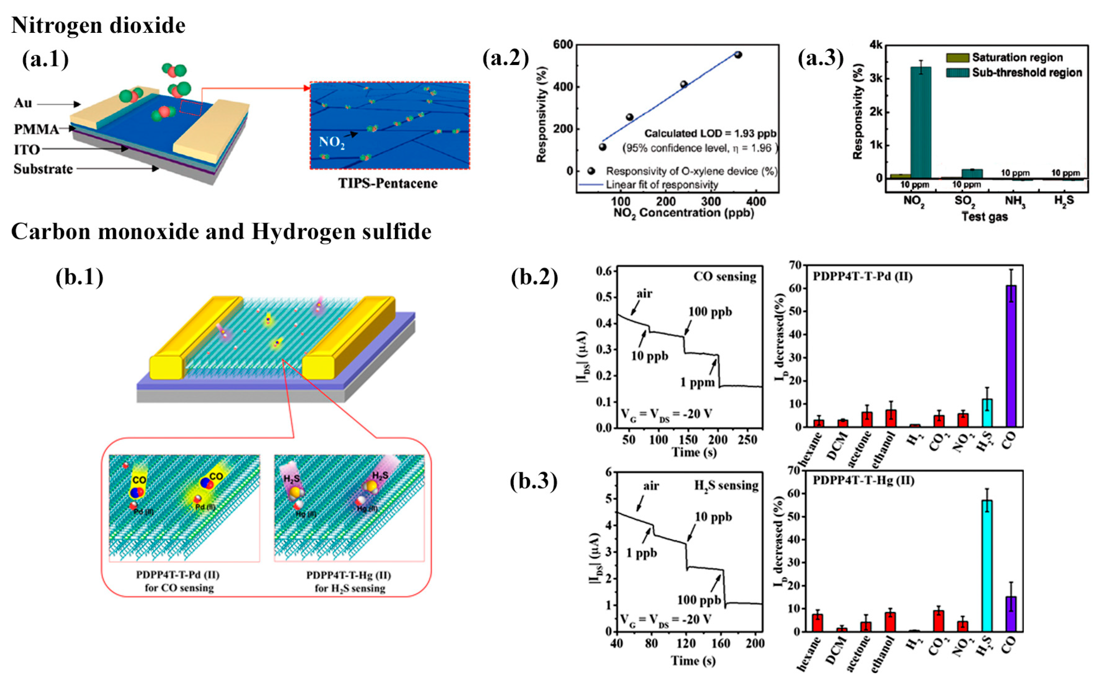
2.5.4. HS and CO
3. Outlook
3.1. Future Prospects
3.2. Conclusions
Author Contributions
Funding
Conflicts of Interest
References
- Zhou, Y.; Han, S.T.; Roy, V. 6-Nanocomposite Dielectric Materials for Organic Flexible Electronics. In Nanocrystalline Materials, 2nd ed.; Tjong, S.C., Ed.; Elsevier: Oxford, UK, 2014; pp. 195–220. [Google Scholar] [CrossRef]
- Chiang, C.K.; Fincher, C.R.; Park, Y.W.; Heeger, A.J.; Shirakawa, H.; Louis, E.J.; Gau, S.C.; MacDiarmid, A.G. Electrical Conductivity in Doped Polyacetylene. Phys. Rev. Lett. 1977, 39, 1098–1101. [Google Scholar] [CrossRef]
- Van Slyke, S.A.; Chen, C.H.; Tang, C.W. Organic electroluminescent devices with improved stability. Appl. Phys. Lett. 1996, 69, 2160–2162. [Google Scholar] [CrossRef]
- Kroto, H.W.; Heath, J.R.; O’Brien, S.C.; Curl, R.F.; Smalley, R.E. C60: Buckminsterfullerene. Nature 1985, 318, 162–163. [Google Scholar] [CrossRef]
- Yu, G.; Gao, J.; Hummelen, J.C.; Wudl, F.; Heeger, A.J. Polymer Photovoltaic Cells: Enhanced Efficiencies via a Network of Internal Donor-Acceptor Heterojunctions. Science 1995, 270, 1789–1791. [Google Scholar] [CrossRef] [Green Version]
- Iijima, S. Helical microtubules of graphitic carbon. Nature 1991, 354, 56–58. [Google Scholar] [CrossRef]
- Novoselov, K.S.; Geim, A.K.; Morozov, S.V.; Jiang, D.; Zhang, Y.; Dubonos, S.V.; Grigorieva, I.V.; Firsov, A.A. Electric Field Effect in Atomically Thin Carbon Films. Science 2004, 306, 666–669. [Google Scholar] [CrossRef] [Green Version]
- Santos, J.C.B.; Paterno, L.G.; Dirani, E.A.T.; Fonseca, F.J.; Andrade, A.M.D. Influence of polyaniline and phthalocyanine hole-transport layers on the electrical performance of light-emitting diodes using MEH-PPV as emissive material. Thin Solid Films 2008, 516, 3184–3188. [Google Scholar] [CrossRef]
- Kumar, L.; Rawal, I.; Kaur, A.; Annapoorni, S. Flexible room temperature ammonia sensor based on polyaniline. Sens. Actuators B Chem. 2017, 240, 408–416. [Google Scholar] [CrossRef]
- Moiz, S.A.; Alahmadi, A.N.M.; Karimov, K.S. Improved organic solar cell by incorporating silver nanoparticles embedded polyaniline as buffer layer. Solid-State Electron. 2020, 163, 107658. [Google Scholar] [CrossRef]
- Zhu, Y.; Murali, S.; Stoller, M.D.; Ganesh, K.J.; Cai, W.; Ferreira, P.J.; Pirkle, A.; Wallace, R.M.; Cychosz, K.A.; Thommes, M.; et al. Carbon-Based Supercapacitors Produced by Activation of Graphene. Science 2011, 332, 1537–1541. [Google Scholar] [CrossRef] [Green Version]
- Britnell, L.; Gorbachev, R.V.; Jalil, R.; Belle, B.D.; Schedin, F.; Mishchenko, A.; Georgiou, T.; Katsnelson, M.I.; Eaves, L.; Morozov, S.V.; et al. Field-Effect Tunneling Transistor Based on Vertical Graphene Heterostructures. Science 2012, 335, 947–950. [Google Scholar] [CrossRef] [PubMed] [Green Version]
- Cai, X.; Sushkov, A.B.; Suess, R.J.; Jadidi, M.M.; Jenkins, G.S.; Nyakiti, L.O.; Myers-Ward, R.L.; Li, S.; Yan, J.; Gaskill, D.K.; et al. Sensitive room-temperature terahertz detection via the photothermoelectric effect in graphene. Nat. Nanotechnol. 2014, 9, 814–819. [Google Scholar] [CrossRef] [PubMed] [Green Version]
- Funaro, M.; Sarno, M.; Ciambelli, P.; Altavilla, C.; Proto, A. Real time radiation dosimeters based on vertically aligned multiwall carbon nanotubes and graphene. Nanotechnology 2013, 24, 075704. [Google Scholar] [CrossRef] [PubMed]
- Ebisawa, F.; Kurokawa, T.; Nara, S. Electrical properties of polyacetylene/polysiloxane interface. J. Appl. Phys. 1983, 54, 3255–3259. [Google Scholar] [CrossRef]
- Kudo, K.; Yamashina, M.; Moriizumi, T. Field Effect Measurement of Organic Dye Films. Jpn. J. Appl. Phys. 1984, 23, 130. [Google Scholar] [CrossRef]
- Tsumura, A.; Koezuka, H.; Ando, T. Macromolecular electronic device: Field-effect transistor with a polythiophene thin film. Appl. Phys. Lett. 1986, 49, 1210–1212. [Google Scholar] [CrossRef]
- Clarisse, C.; Riou, M.T.; Gauneau, M.; Contellec, M.L. Field-effect transistor with diphthalocyanine thin film. Electron. Lett. 1988, 24, 674–675. [Google Scholar] [CrossRef]
- Horowitz, G.; Fichou, D.; Peng, X.; Xu, Z.; Garnier, F. A field-effect transistor based on conjugated alpha-sexithienyl. Solid State Commun. 1989, 72, 381–384. [Google Scholar] [CrossRef]
- Haddon, R.C.; Perel, A.S.; Morris, R.C.; Palstra, T.T.M.; Hebard, A.F.; Fleming, R.M. C60 thin film transistors. Appl. Phys. Lett. 1995, 67, 121–123. [Google Scholar] [CrossRef] [Green Version]
- Lin, Y.Y.; Gundlach, D.; Nelson, S.; Jackson, T. Stacked pentacene layer organic thin-film transistors with improved characteristics. IEEE Electron. Device Lett. 1997, 18, 606–608. [Google Scholar] [CrossRef]
- Tans, S.J.; Verschueren, A.R.M.; Dekker, C. Room-temperature transistor based on a single carbon nanotube. Nature 1998, 393, 49–52. [Google Scholar] [CrossRef]
- Sisto, T.J.; Zakharov, L.N.; White, B.M.; Jasti, R. Towards pi-extended cycloparaphenylenes as seeds for CNT growth: Investigating strain relieving ring-openings and rearrangements. Chem. Sci. 2016, 7, 3681–3688. [Google Scholar] [CrossRef] [Green Version]
- Terrones, M. Science and Technology of the Twenty-First Century: Synthesis, Properties, and Applications of Carbon Nanotubes. Annu. Rev. Mater. Res. 2003, 33, 419–501. [Google Scholar] [CrossRef]
- Myny, K.; Veenendaal, E.V.; Gelinck, G.H.; Genoe, J.; Dehaene, W.; Heremans, P. An 8-Bit, 40-Instructions- Per-Second Organic Microprocessor on Plastic Foil. IEEE J. Solid-State Circuits 2012, 47, 284–291. [Google Scholar] [CrossRef]
- Yaglioglu, B.; Agostinelli, T.; Cain, P.; Mijalkovic, S.; Nejim, A. Parameter Extraction and Evaluation of UOTFT Model for Organic Thin-Film Transistor Circuit Design. J. Disp. Technol. 2013, 9, 890–894. [Google Scholar] [CrossRef]
- Gelinck, G.H.; Huitema, H.E.A.; van Veenendaal, E.; Cantatore, E.; Schrijnemakers, L.; van der Putten, J.B.P.H.; Geuns, T.C.T.; Beenhakkers, M.; Giesbers, J.B.; Huisman, B.H.; et al. Flexible active- matrix displays and shift registers based on solution-processed organic transistors. Nat. Mater. 2004, 3, 106–110. [Google Scholar] [CrossRef]
- Noda, M.; Kobayashi, N.; Katsuhara, M.; Yumoto, A.; Ushikura, S.I.; Yasuda, R.I.; Hirai, N.; Yukawa, G.; Yagi, I.; Nomoto, K.; et al. 47.3: A Rollable AM-OLED Display Driven by OTFTs. SID Symp. Dig. Tech. Pap. 2010, 41, 710. [Google Scholar] [CrossRef]
- Kiew, S.F.; Kiew, L.V.; Lee, H.B.; Imae, T.; Chung, L.Y. Assessing biocompatibility of graphene oxide-based nanocarriers: A review. J. Control. Release 2016, 226, 217–228. [Google Scholar] [CrossRef]
- Twenty-five years of conducting polymers. Chem. Commun. 2003, 1–4. [CrossRef]
- Geim, A.K.; Novoselov, K.S. The rise of graphene. Nat. Mater. 2007, 6, 183–191. [Google Scholar] [CrossRef] [PubMed]
- Horowitz, G.; Lang, P.; Mottaghi, M.; Aubin, H. Extracting Parameters from the Current–Voltage Characteristics of Organic Field-Effect Transistors. Adv. Funct. Mater. 2004, 14, 1069–1074. [Google Scholar] [CrossRef]
- Natali, D.; Fumagalli, L.; Sampietro, M. Modeling of organic thin film transistors: Effect of contact resistances. J. Appl. Phys. 2007, 101, 014501. [Google Scholar] [CrossRef]
- Deen, M.J.; Marinov, O.; Zschieschang, U.; Klauk, H. Organic Thin-Film Transistors: Part II—Parameter Extraction. IEEE Trans. Electron. Device 2009, 56, 2962–2968. [Google Scholar] [CrossRef]
- Natali, D.; Caironi, M. Charge Injection in Solution-Processed Organic Field-Effect Transistors: Physics, Models and Characterization Methods. Adv. Mater. 2012, 24, 1357–1387. [Google Scholar] [CrossRef]
- Kumar, B.; Kaushik, B.K.; Negi, Y.S. Organic Thin Film Transistors: Structures, Models, Materials, Fabrication, and Applications: A Review. Polym. Rev. 2014, 54, 33–111. [Google Scholar] [CrossRef]
- Fumagalli, L.; Natali, D.; Sampietro, M.; Peron, E.; Perissinotti, F.; Tallarida, G.; Ferrari, S. Al2O3 as gate dielectric for organic transistors: Charge transport phenomena in poly-(3-hexylthiophene) based devices. Org. Electron. 2008, 9, 198–208. [Google Scholar] [CrossRef]
- Di Pietro, R.; Venkateshvaran, D.; Klug, A.; List-Kratochvil, E.J.W.; Facchetti, A.; Sirringhaus, H.; Neher, D. Simultaneous extraction of charge density dependent mobility and variable contact resistance from thin film transistors. Appl. Phys. Lett. 2014, 104, 193501. [Google Scholar] [CrossRef] [Green Version]
- Cavallari, M.R.; Izquierdo, J.E.E.; García, D.C.; Nogueira, V.A.M.; Oliveira, J.D.S.; Pastrana, L.M.; Kymissis, I.; Fonseca, F.J. Cross-linked polyvinyl phenol as dielectric for flexible bottom gate bottom contact transistors. In Proceedings of the 2019 34th Symposium on Microelectronics Technology and Devices (SBMicro), São Paulo, Brazil, 26–30 August 2019; pp. 1–3. [Google Scholar] [CrossRef]
- Sirringhaus, H.; Tessler, N.; Friend, R. Integrated, high-mobility polymer field-effect transistors driving polymer light-emitting diodes. Synth. Met. 1999, 102, 857–860. [Google Scholar] [CrossRef]
- Deen, M.J.; Marinov, O.; Holdcroft, S.; Woods, W. Low-frequency noise in polymer transistors. IEEE Trans. Electron. Device 2001, 48, 1688–1695. [Google Scholar] [CrossRef]
- Fu, Y.; Lin, C.; Tsai, F.Y. High field-effect mobility from poly(3-hexylthiophene) thin-film transistors by solvent–vapor-induced reflow. Org. Electron. 2009, 10, 883–888. [Google Scholar] [CrossRef]
- Knipp, D.; Street, R.A.; Völkel, A.; Ho, J. Pentacene thin film transistors on inorganic dielectrics: Morphology, structural properties, and electronic transport. J. Appl. Phys. 2003, 93, 347–355. [Google Scholar] [CrossRef]
- Lee, K.; Smith, T.; Dickey, K.; Yoo, J.; Stevenson, K.; Loo, Y.L. High-Resolution Characterization of Pentacene/Polyaniline Interfaces in Thin-Film Transistors. Adv. Funct. Mater. 2006, 16, 2409–2414. [Google Scholar] [CrossRef]
- Mottaghi, M.; Horowitz, G. Field-induced mobility degradation in pentacene thin-film transistors. Org. Electron. 2006, 7, 528–536. [Google Scholar] [CrossRef]
- Tiwari, S.P.; Knauer, K.A.; Dindar, A.; Kippelen, B. Performance comparison of pentacene organic field-effect transistors with SiO2 modified with octyltrichlorosilane or octadecyltrichlorosilane. Org. Electron. 2012, 13, 18–22. [Google Scholar] [CrossRef]
- Gold, H.; Haase, A.; Fian, A.; Prietl, C.; Striedinger, B.; Zanella, F.; Marjanović, N.; Ferrini, R.; Ring, J.; Lee, K.D.; et al. Self-aligned flexible organic thin-film transistors with gates patterned by nano-imprint lithography. Org. Electron. 2015, 22, 140–146. [Google Scholar] [CrossRef]
- Ha, T.J.; Sparrowe, D.; Dodabalapur, A. Device architectures for improved amorphous polymer semiconductor thin-film transistors. Org. Electron. 2011, 12, 1846–1851. [Google Scholar] [CrossRef]
- Hwang, D.K.; Lee, K.; Kim, J.H.; Im, S.; Kim, C.S.; Baik, H.K.; Park, J.H.; Kim, E. Low-voltage high-mobility pentacene thin-film transistors with polymer/high-k oxide double gate dielectrics. Appl. Phys. Lett. 2006, 88, 243513. [Google Scholar] [CrossRef]
- Acton, O.; Ting, G.; Ma, H.; Ka, J.W.; Yip, H.L.; Tucker, N.M.; Jen, A.K.Y. π-σ-Phosphonic Acid Organic Monolayer/Sol–Gel Hafnium Oxide Hybrid Dielectrics for Low-Voltage Organic Transistors. Adv. Mater. 2008, 20, 3697–3701. [Google Scholar] [CrossRef]
- Xu, W.; Rhee, S.W. Low-operating voltage organic field-effect transistors with high-k cross-linked cyanoethylated pullulan polymer gate dielectrics. J. Mater. Chem. 2009, 19, 5250–5257. [Google Scholar] [CrossRef] [Green Version]
- Ortiz, R.P.; Facchetti, A.; Marks, T.J. High-k Organic, Inorganic, and Hybrid Dielectrics for Low-Voltage Organic Field-Effect Transistors. Chem. Rev. 2010, 110, 205–239. [Google Scholar] [CrossRef]
- Zhao, X.; Wang, S.; Li, A.; Ouyang, J.; Xia, G.; Zhou, J. Universal solution-processed high-k amorphous oxide dielectrics for high-performance organic thin film transistors. RSC Adv. 2014, 4, 14890–14895. [Google Scholar] [CrossRef]
- Torres, I.; Taylor, D.M.; Itoh, E. Interface states and depletion-induced threshold voltage instabilityin organic metal-insulator-semiconductor structures. Appl. Phys. Lett. 2004, 85, 314–316. [Google Scholar] [CrossRef]
- Braga, D.; Horowitz, G. Subthreshold regime in rubrene single-crystal organic transistors. Appl. Phys. A 2009, 95, 193–201. [Google Scholar] [CrossRef]
- Stadler, P.; Track, A.M.; Ullah, M.; Sitter, H.; Matt, G.J.; Koller, G.; Singh, T.B.; Neugebauer, H.; Sariciftci, N.S.; Ramsey, M.G. The role of the dielectric interface in organic transistors: A combined device and photoemission study. Org. Electron. 2010, 11, 207–211. [Google Scholar] [CrossRef]
- Klauk, H.; Halik, M.; Zschieschang, U.; Schmid, G.; Radlik, W.; Weber, W. High-mobility polymer gate dielectric pentacene thin film transistors. J. Appl. Phys. 2002, 92, 5259–5263. [Google Scholar] [CrossRef]
- Cavallari, M.R.; Zanchin, V.R.; Valle, M.A.; Izquierdo, J.E.E.; Rodríguez, E.M.; Rodríguez, E.F.G.; Pereira-da-Silva, M.A.; Fonseca, F.J. On the Performance Degradation of Poly(3-Hexylthiophene) Field-Effect Transistors. IEEE Trans. Device Mater. Reliab. 2015, 15, 342–351. [Google Scholar] [CrossRef]
- Gomes, H.L.; Stallinga, P.; Dinelli, F.; Murgia, M.; Biscarini, F.; de Leeuw, D.M.; Muck, T.; Geurts, J.; Molenkamp, L.W.; Wagner, V. Bias-induced threshold voltages shifts in thin-film organic transistors. Appl. Phys. Lett. 2004, 84, 3184–3186. [Google Scholar] [CrossRef] [Green Version]
- Sirringhaus, H.; Friend, R.H.; Li, X.C.; Moratti, S.C.; Holmes, A.B.; Feeder, N. Bis(dithienothiophene) organic field-effect transistors with a high ON/OFF ratio. Appl. Phys. Lett. 1997, 71, 3871–3873. [Google Scholar] [CrossRef]
- Gelinck, G.; Heremans, P.; Nomoto, K.; Anthopoulos, T.D. Organic Transistors in Optical Displays and Microelectronic Applications. Adv. Mater. 2010, 22, 3778–3798. [Google Scholar] [CrossRef]
- Yu, S.; Kim, J.S.; Jeon, P.J.; Ahn, J.; Park, J.C.; Im, S. Transition Metal Dichalcogenide-Based Transistor Circuits for Gray Scale Organic Light-Emitting Displays. Adv. Funct. Mater. 2017, 27, 1603682. [Google Scholar] [CrossRef]
- Choi, M.; Park, Y.J.; Sharma, B.K.; Bae, S.R.; Kim, S.Y.; Ahn, J.H. Flexible active-matrix organic light-emitting diode display enabled by MoS2 thin-film transistor. Sci. Adv. 2018, 4, eaas8721. [Google Scholar] [CrossRef] [PubMed] [Green Version]
- Kwon, H.; Garg, S.; Park, J.H.; Jeong, Y.; Yu, S.; Kim, S.M.; Kung, P.; Im, S. Monolayer MoS2 field-effect transistors patterned by photolithography for active matrix pixels in organic light-emitting diodes. NPJ 2D Mater. Appl. 2019, 3, 9. [Google Scholar] [CrossRef]
- Scheinert, S.; Paasch, G.; Doll, T. The influence of bulk traps on the subthreshold characteristics of an organic field effect transistor. Synth. Met. 2003, 139, 233–237. [Google Scholar] [CrossRef]
- McDowell, M.; Hill, I.G.; McDermott, J.E.; Bernasek, S.L.; Schwartz, J. Improved organic thin-film transistor performance using novel self-assembled monolayers. Appl. Phys. Lett. 2006, 88, 073505. [Google Scholar] [CrossRef] [Green Version]
- Liu, Z.; Oh, J.H.; Roberts, M.E.; Wei, P.; Paul, B.C.; Okajima, M.; Nishi, Y.; Bao, Z. Solution-processed flexible organic transistors showing very-low subthreshold slope with a bilayer polymeric dielectric on plastic. Appl. Phys. Lett. 2009, 94, 203301. [Google Scholar] [CrossRef] [Green Version]
- Blülle, B.; Häusermann, R.; Batlogg, B. Approaching the Trap-Free Limit in Organic Single-Crystal Field-Effect Transistors. Phys. Rev. Appl. 2014, 1, 034006. [Google Scholar] [CrossRef] [Green Version]
- Bock, C.; Pham, D.V.; Kunze, U.; Käfer, D.; Witte, G.; Wöll, C. Improved morphology and charge carrier injection in pentacene field-effect transistors with thiol-treated electrodes. J. Appl. Phys. 2006, 100, 114517. [Google Scholar] [CrossRef]
- Cavallari, M.R.; Izquierdo, J.E.E.; Braga, G.S.; Dirani, E.A.T.; Pereira-da Silva, M.A.; Rodríguez, E.F.G.; Fonseca, F.J. Enhanced Sensitivity of Gas Sensor Based on Poly(3-hexylthiophene) Thin-Film Transistors for Disease Diagnosis and Environment Monitoring. Sensors 2015, 15, 9592–9609. [Google Scholar] [CrossRef] [Green Version]
- Zhou, X.; Niu, K.; Wang, Z.; Huang, L.; Chi, L. An ammonia detecting mechanism for organic transistors as revealed by their recovery processes. Nanoscale 2018, 10, 8832–8839. [Google Scholar] [CrossRef]
- Sizov, A.S.; Trul, A.A.; Chekusova, V.; Borshchev, O.V.; Vasiliev, A.A.; Agina, E.V.; Ponomarenko, S.A. Highly Sensitive Air-Stable Easily Processable Gas Sensors Based on Langmuir–Schaefer Monolayer Organic Field-Effect Transistors for Multiparametric H2S and NH3 Real-Time Detection. ACS Appl. Mater. Interfaces 2018, 10, 43831–43841. [Google Scholar] [CrossRef]
- Park, M.S.; Meresa, A.A.; Kwon, C.M.; Kim, F.S. Selective Wet-Etching of Polymer/Fullerene Blend Films for Surface- and Nanoscale Morphology-Controlled Organic Transistors and Sensitivity-Enhanced Gas Sensors. Polymers 2019, 11, 1682. [Google Scholar] [CrossRef] [PubMed] [Green Version]
- Huang, W.; Yu, J.; Yu, X.; Shi, W. Polymer dielectric layer functionality in organic field-effect transistor based ammonia gas sensor. Org. Electron. 2013, 14, 3453–3459. [Google Scholar] [CrossRef]
- Elkington, D.; Cooling, N.; Belcher, W.; Dastoor, P.; Zhou, X. Organic Thin-Film Transistor (OTFT)-Based Sensors. Electronics 2014, 3, 234–254. [Google Scholar] [CrossRef] [Green Version]
- Zhang, C.; Chen, P.; Hu, W. Organic field-effect transistor-based gas sensors. Chem. Soc. Rev. 2015, 44, 2087–2107. [Google Scholar] [CrossRef] [PubMed] [Green Version]
- Lv, A.; Pan, Y.; Chi, L. Gas Sensors Based on Polymer Field-Effect Transistors. Sensors 2017, 17, 213. [Google Scholar] [CrossRef] [Green Version]
- Nketia-Yawson, B.; Noh, Y.Y. Organic thin film transistor with conjugated polymers for highly sensitive gas sensors. Macromol. Res. 2017, 25, 489–495. [Google Scholar] [CrossRef]
- Surya, S.G.; Raval, H.N.; Ahmad, R.; Sonar, P.; Salama, K.N.; Rao, V. Organic field effect transistors (OFETs) in environmental sensing and health monitoring: A review. TrAC Trends Anal. Chem. 2019, 111, 27–36. [Google Scholar] [CrossRef]
- Mun, S.; Park, Y.; Lee, Y.E.K.; Sung, M.M. Highly Sensitive Ammonia Gas Sensor Based on Single-Crystal Poly(3-hexylthiophene) (P3HT) Organic Field Effect Transistor. Langmuir 2017, 33, 13554–13560. [Google Scholar] [CrossRef]
- Rajeev, V.; Paulose, A.K.; Unni, K.N. Ammonia gas detection using field-effect transistor based on a solution-processable organic semiconductor. Vacuum 2018, 158, 271–277. [Google Scholar] [CrossRef]
- Wei, S.; Tian, F.; Ge, F.; Wang, X.; Zhang, G.; Lu, H.; Yin, J.; Wu, Z.; Qiu, L. Helical Nanofibrils of Block Copolymer for High-Performance Ammonia Sensors. ACS Appl. Mater. Interfaces 2018, 10, 22504–22512. [Google Scholar] [CrossRef]
- Lu, J.; Liu, D.; Zhou, J.; Chu, Y.; Chen, Y.; Wu, X.; Huang, J. Porous Organic Field-Effect Transistors for Enhanced Chemical Sensing Performances. Adv. Funct. Mater. 2017, 27, 1700018. [Google Scholar] [CrossRef]
- Sahu, P.K.; Pandey, M.; Kumar, C.; Pandey, S.S.; Takashima, W.; Mishra, V.; Prakash, R. Air-stable vapor phase sensing of ammonia in sub-threshold regime of poly(2,5-bis(3-tetradecylthiophen-2yl)thieno(3,2-b)thiophene) based polymer thin-film transistor. Sens. Actuators B Chem. 2017, 246, 243–251. [Google Scholar] [CrossRef]
- Zhang, F.; Qu, G.; Mohammadi, E.; Mei, J.; Diao, Y. Solution-Processed Nanoporous Organic Semiconductor Thin Films: Toward Health and Environmental Monitoring of Volatile Markers. Adv. Funct. Mater. 2017, 27, 1701117. [Google Scholar] [CrossRef]
- Chen, Y.; Kong, X.; Lu, G.; Qi, D.; Wu, Y.; Li, X.; Bouvet, M.; Sun, D.; Jiang, J. The lower rather than higher density charge carrier determines the NH3-sensing nature and sensitivity of ambipolar organic semiconductors. Mater. Chem. Front. 2018, 2, 1009–1016. [Google Scholar] [CrossRef]
- Kumar, C.; Rawat, G.; Kumar, H.; Kumar, Y.; Kumar, A.; Prakash, R.; Jit, S. Electrical and ammonia gas sensing properties of PQT-12/CdSe quantum dots composite-based organic thin film transistors. IEEE Sens. J. 2018, 18, 6085–6091. [Google Scholar] [CrossRef]
- Lu, C.F.; Shih, C.W.; Chen, C.A.; Chin, A.; Su, W.F. Tuning the Morphology of Isoindigo Donor–Acceptor Polymer Film for High Sensitivity Ammonia Sensor. Adv. Funct. Mater. 2018, 28, 1803145. [Google Scholar] [CrossRef]
- Wu, S.; Wang, G.; Xue, Z.; Ge, F.; Zhang, G.; Lu, H.; Qiu, L. Organic Field-Effect Transistors with Macroporous Semiconductor Films as High-Performance Humidity Sensors. ACS Appl. Mater. Interfaces 2017, 9, 14974–14982. [Google Scholar] [CrossRef]
- Besar, K.; Dailey, J.; Katz, H.E. Ethylene Detection Based on Organic Field-Effect Transistors with Porogen and Palladium Particle Receptor Enhancements. ACS Appl. Mater. Interfaces 2017, 9, 1173–1177. [Google Scholar] [CrossRef]
- Lv, A.; Wang, M.; Wang, Y.; Bo, Z.; Chi, L. Investigation into the Sensing Process of High-Performance H2S Sensors Based on Polymer Transistors. Chem. A Eur. J. 2016, 22, 3654–3659. [Google Scholar] [CrossRef]
- Song, Z.; Liu, G.; Tang, Q.; Zhao, X.; Tong, Y.; Liu, Y. Controllable gas selectivity at room temperature based on Ph5T2-modified CuPc nanowire field-effect transistors. Org. Electron. 2017, 48, 68–76. [Google Scholar] [CrossRef]
- Yang, Y.; Liu, Z.; Chen, L.; Yao, J.; Lin, G.; Zhang, X.; Zhang, G.; Zhang, D. Conjugated Semiconducting Polymer with Thymine Groups in the Side Chains: Charge Mobility Enhancement and Application for Selective Field-Effect Transistor Sensors toward CO and H2S. Chem. Mater. 2019, 31, 1800–1807. [Google Scholar] [CrossRef]
- Yang, Y.; Katz, H.E. Hybrid of P3HT and ZnO@GO nanostructured particles for increased NO2 sensing response. J. Mater. Chem. C 2017, 5, 2160–2166. [Google Scholar] [CrossRef]
- Lee, J.H.; Seo, Y.; Park, Y.D.; Anthony, J.E.; Kwak, D.H.; Lim, J.A.; Ko, S.; Jang, H.W.; Cho, K.; Lee, W.H. Effect of Crystallization Modes in TIPS-pentacene/Insulating Polymer Blends on the Gas Sensing Properties of Organic Field-Effect Transistors. Sci. Rep. 2019, 9, 21. [Google Scholar] [CrossRef] [PubMed] [Green Version]
- Shao, B.; Liu, Y.; Zhuang, X.; Hou, S.; Han, S.; Yu, X.; Yu, J. Crystallinity and grain boundary control of TIPS-pentacene in organic thin-film transistors for the ultra-high sensitive detection of NO2. J. Mater. Chem. C 2019, 7, 10196–10202. [Google Scholar] [CrossRef]
- Seo, Y.; Lee, J.H.; Anthony, J.E.; Nguyen, K.V.; Kim, Y.H.; Jang, H.W.; Ko, S.; Cho, Y.; Lee, W.H. Effects of Grain Boundary Density on the Gas Sensing Properties of Triethylsilylethynyl-Anthradithiophene Field-Effect Transistors. Adv. Mater. Interfaces 2018, 5, 1701399. [Google Scholar] [CrossRef]
- Han, S.; Zhuang, X.; Shi, W.; Yang, X.; Li, L.; Yu, J. Poly(3-hexylthiophene)/polystyrene (P3HT/PS) blends based organic field-effect transistor ammonia gas sensor. Sens. Actuators B Chem. 2016, 225, 10–15. [Google Scholar] [CrossRef]
- Jeong, S.H.; Lee, J.Y.; Lim, B.; Lee, J.; Noh, Y.Y. Diketopyrrolopyrrole-based conjugated polymer for printed organic field-effect transistors and gas sensors. Dyes Pigment. 2017, 140, 244–249. [Google Scholar] [CrossRef]
- Nketia-Yawson, B.; Jung, A.R.; Noh, Y.; Ryu, G.S.; Tabi, G.D.; Lee, K.K.; Kim, B.; Noh, Y.Y. Highly Sensitive Flexible NH3 Sensors Based on Printed Organic Transistors with Fluorinated Conjugated Polymers. ACS Appl. Mater. Interfaces 2017, 9, 7322–7330. [Google Scholar] [CrossRef]
- Hou, S.; Zhuang, X.; Yang, Z.; Yu, J. Effect of Vertical Annealing on the Nitrogen Dioxide Response of Organic Thin Film Transistors. Nanomaterials 2018, 8, 203. [Google Scholar] [CrossRef] [Green Version]
- Zhuang, X.; Han, S.; Huai, B.; Shi, W.; Junsheng, Y. Sub-ppm and high response organic thin-film transistor NO2 sensor based on nanofibrillar structured TIPS-pentacene. Sens. Actuators B Chem. 2019, 279, 238–244. [Google Scholar] [CrossRef]
- Zhuang, X.; Huang, W.; Han, S.; Jiang, Y.; Zheng, H.; Yu, J. Interfacial modifying layer-driven high-performance organic thin-film transistors and their nitrogen dioxide gas sensors. Org. Electron. 2017, 49, 334–339. [Google Scholar] [CrossRef]
- Kumar, A.; Jha, P.; Singh, A.; Chauhan, A.; Gupta, S.; Aswal, D.; Muthe, K.; Gadkari, S. Modeling of gate bias controlled NO2 response of the PCDTBT based organic field effect transistor. Chem. Phys. Lett. 2018, 698, 7–10. [Google Scholar] [CrossRef]
- Han, S.; Yang, Z.; Li, Z.; Zhuang, X.; Akinwande, D.; Yu, J. Improved Room Temperature NO2 Sensing Performance of Organic Field-Effect Transistor by Directly Blending a Hole-Transporting/Electron-Blocking Polymer into the Active Layer. ACS Appl. Mater. Interfaces 2018, 10, 38280–38286. [Google Scholar] [CrossRef] [PubMed]
- Yang, J.; Xie, G.; Su, Y.; Zhang, Q.; Du, H.; Tai, H.; Du, X.; Jiang, Y. Flexible organic thin-film transistors based on poly(3-hexylthiophene) films for nitrogen dioxide detection. Sci. China Technol. Sci. 2018, 61, 1696–1704. [Google Scholar] [CrossRef]
- Huang, W.; Zhuang, X.; Melkonyan, F.S.; Wang, B.; Zeng, L.; Wang, G.; Han, S.; Bedzyk, M.J.; Yu, J.; Marks, T.J.; et al. UV–Ozone Interfacial Modification in Organic Transistors for High-Sensitivity NO2 Detection. Adv. Mater. 2017, 29, 1701706. [Google Scholar] [CrossRef] [PubMed]
- Gonzalez-Macia, L.; Killard, A. 4 - Screen printing and other scalable point of care (POC) biosensor processing technologies. In Medical Biosensors for Point of Care (POC) Applications; Narayan, R.J., Ed.; Woodhead Publishing: Cambridge, UK, 2017; pp. 69–98. [Google Scholar] [CrossRef]
- Diao, Y.; Shaw, L.; Bao, Z.; Mannsfeld, S.C.B. Morphology control strategies for solution-processed organic semiconductor thin films. Energy Environ. Sci. 2014, 7, 2145–2159. [Google Scholar] [CrossRef] [Green Version]
- Park, S.I.; Quan, Y.J.; Kim, S.H.; Kim, H.; Kim, S.; Chun, D.M.; Lee, C.S.; Taya, M.; Chu, W.S.; Ahn, S.H. A review on fabrication processes for electrochromic devices. Int. J. Precis. Eng. Manuf.-Green Technol. 2016, 3, 397–421. [Google Scholar] [CrossRef]
- Chung, S.; Cho, K.; Lee, T. Recent Progress in Inkjet-Printed Thin-Film Transistors. Adv. Sci. 2019, 6, 1801445. [Google Scholar] [CrossRef]
- Minemawari, H.; Yamada, T.; Matsui, H.; Tsutsumi, J.; Haas, S.; Chiba, R.; Kumai, R.; Hasegawa, T. Inkjet printing of single-crystal films. Nature 2011, 475, 364–367. [Google Scholar] [CrossRef]
- Yang, S.; Park, S.; Bintinger, J.; Bonnassieux, Y.; Anthony, J.; Kymissis, I. Employing Pneumatic Nozzle Printing for Controlling the Crystal Growth of Small Molecule Organic Semiconductor for Field-Effect Transistors. Adv. Electron. Mater. 2018, 4, 1700534. [Google Scholar] [CrossRef]
- Diao, Y.; Tee, B.C.K.; Giri, G.; Xu, J.; Kim, D.H.; Becerril, H.A.; Stoltenberg, R.M.; Lee, T.H.; Xue, G.; Mannsfeld, S.C.B.; et al. Solution coating of large-area organic semiconductor thin films with aligned single-crystalline domains. Nat. Mater. 2013, 12, 665–671. [Google Scholar] [CrossRef] [PubMed]
- de Oliveira, R.; de Barros, A.; Ferreira, M. 4-Nanostructured Films: Langmuir–Blodgett (LB) and Layer-by-Layer (LbL) Techniques. In Nanostructures; Da Róz, A.L., Ferreira, M., de Lima Leite, F., Oliveira, O.N., Eds.; William Andrew Publishing: Norwich, NY, USA, 2017; pp. 105–123. [Google Scholar] [CrossRef]
- Yuan, Y.; Giri, G.; Ayzner, A.L.; Zoombelt, A.P.; Mannsfeld, S.C.B.; Chen, J.; Nordlund, D.; Toney, M.F.; Huang, J.; Bao, Z. Ultra-high mobility transparent organic thin film transistors grown by an off-centre spin-coating method. Nat. Commun. 2014, 5, 3005. [Google Scholar] [CrossRef] [PubMed] [Green Version]
- Yamao, T.; Ota, S.; Miki, T.; Hotta, S.; Azumi, R. Improved sublimation growth of single crystals of thiophene/phenylene co-oligomers. Thin Solid Films 2008, 516, 2527–2531. [Google Scholar] [CrossRef]
- Keeney, M.; Jiang, X.Y.; Yamane, M.; Lee, M.; Goodman, S.; Yang, F. Nanocoating for biomolecule delivery using layer-by-layer self-assembly. J. Mater. Chem. B 2015, 3, 8757–8770. [Google Scholar] [CrossRef] [PubMed] [Green Version]
- Han, U.; Seo, Y.; Hong, J. Effect of pH on the structure and drug release profiles of layer-by-layer assembled films containing polyelectrolyte, micelles, and graphene oxide. Sci. Rep. 2016, 6, 24158. [Google Scholar] [CrossRef]
- Casalini, S.; Bortolotti, C.A.; Leonardi, F.; Biscarini, F. Self-assembled monolayers in organic electronics. Chem. Soc. Rev. 2017, 46, 40–71. [Google Scholar] [CrossRef]
- Yang, Y.; Liu, C.; Gao, S.; Li, Y.; Wang, X.; Wang, Y.; Minari, T.; Xu, Y.; Wang, P.; Zhao, Y.; et al. Large [6,6]-phenyl C61 butyric acid methyl (PCBM) hexagonal crystals grown by solvent-vapor annealing. Mater. Chem. Phys. 2014, 145, 327–333. [Google Scholar] [CrossRef]
- Liu, C.; Minari, T.; Lu, X.; Kumatani, A.; Takimiya, K.; Tsukagoshi, K. Solution-Processable Organic Single Crystals with Bandlike Transport in Field-Effect Transistors. Adv. Mater. 2011, 23, 523–526. [Google Scholar] [CrossRef]
- Han, S.; Jeong, H.; Jang, H.; Baek, S.; Kim, S.H.; Lee, H.S. Exploring the ultrasonic nozzle spray-coating technique for the fabrication of solution-processed organic electronics. Org. Electron. 2017, 49, 212–217. [Google Scholar] [CrossRef]
- Wu, X.; Surendran, A.; Moser, M.; Chen, S.; Muhammad, B.T.; Maria, I.P.; McCulloch, I.; Leong, W.L. Universal Spray-Deposition Process for Scalable, High-Performance, and Stable Organic Electrochemical Transistors. ACS Appl. Mater. Interfaces 2020, 12, 20757–20764. [Google Scholar] [CrossRef]
- Reese, C.; Bao, Z. Organic single-crystal field-effect transistors. Mater. Today 2007, 10, 20–27. [Google Scholar] [CrossRef]
- Pandey, M.; Nagamatsu, S.; Pandey, S.S.; Hayase, S.; Takashima, W. Enhancement of carrier mobility along with anisotropic transport in non-regiocontrolled poly (3-hexylthiophene) films processed by floating film transfer method. Org. Electron. 2016, 38, 115–120. [Google Scholar] [CrossRef]
- Kumar, C.; Rawat, G.; Kumar, H.; Kumar, Y.; Prakash, R.; Jit, S. Electrical and ammonia gas sensing properties of poly(3,3′′′-dialkylquaterthiophene) based organic thin film transistors fabricated by floating-film transfer method. Org. Electron. 2017, 48, 53–60. [Google Scholar] [CrossRef]
- Alexandrou, K.; Petrone, N.; Hone, J.; Kymissis, I. Encapsulated graphene field-effect transistors for air stable operation. Appl. Phys. Lett. 2015, 106, 113104. [Google Scholar] [CrossRef]
- Søndergaard, R.R.; Hösel, M.; Krebs, F.C. Roll-to-Roll fabrication of large area functional organic materials. J. Polym. Sci. Part B Polym. Phys. 2013, 51, 16–34. [Google Scholar] [CrossRef]
- Amorim, C.; Cavallari, M.; Santos, G.; Fonseca, F.; Andrade, A.; Mergulhão, S. Determination of carrier mobility in MEH-PPV thin-films by stationary and transient current techniques. J. Non-Cryst. Solids 2012, 358, 484–491. [Google Scholar] [CrossRef]
- da Silva, M.F.P.; de Oliveira, D.R.; Cavallari, M.R.; Dirani, E.A.T.; Triboni, E.R.; Paterno, L.G.; Fonseca, F.J.; Ando, R.A.; da Silva Baptista, M.; Landers, R.; et al. A simple visible light photo-assisted method for assembling and curing multilayer GO thin films. Mater. Chem. Phys. 2015, 165, 125–133. [Google Scholar] [CrossRef]
- Cavallari, M.R.; Braga, G.S.; da Silva, M.F.; Izquierdo, J.E.; Paterno, L.G.; Dirani, E.A.; Kymissis, I.; Fonseca, F.J. A Hybrid Electronic Nose and Tongue for the Detection of Ketones: Improved Sensor Orthogonality Using Graphene Oxide-Based Detectors. IEEE Sens. J. 2017, 17, 1971–1980. [Google Scholar] [CrossRef]
- Papamatthaiou, S.; Argyropoulos, D.P.; Masurkar, A.; Cavallari, M.R.; Farmakis, F.; Kymissis, I.; Georgoulas, N. Permanent water swelling effect in low temperature thermally reduced graphene oxide. Appl. Phys. Lett. 2017, 110, 252106. [Google Scholar] [CrossRef] [Green Version]
- Su, W.P.; Schrieffer, J.R.; Heeger, A.J. Solitons in Polyacetylene. Phys. Rev. Lett. 1979, 42, 1698–1701. [Google Scholar] [CrossRef]
- Brédas, J.L.; Chance, R.R.; Silbey, R. Comparative theoretical study of the doping of conjugated polymers: Polarons in polyacetylene and polyparaphenylene. Phys. Rev. B 1982, 26, 5843–5854. [Google Scholar] [CrossRef] [Green Version]
- Castro Neto, A.H.; Guinea, F.; Peres, N.M.R.; Novoselov, K.S.; Geim, A.K. The electronic properties of graphene. Rev. Mod. Phys. 2009, 81, 109–162. [Google Scholar] [CrossRef] [Green Version]
- Bansal, T.; Mohite, A.D.; Shah, H.M.; Galande, C.; Srivastava, A.; Jasinski, J.B.; Ajayan, P.M.; Alphenaar, B.W. New insights into the density of states of graphene oxide using capacitive photocurrent spectroscopy. Carbon 2012, 50, 808–814. [Google Scholar] [CrossRef]
- Skákalová, V.; Kaiser, A.B.; Woo, Y.S.; Roth, S. Electronic transport in carbon nanotubes: From individual nanotubes to thin and thick networks. Phys. Rev. B 2006, 74, 085403. [Google Scholar] [CrossRef]
- Basu, S.; Bhattacharyya, P. Recent developments on graphene and graphene oxide based solid state gas sensors. Sens. Actuators B Chem. 2012, 173, 1–21. [Google Scholar] [CrossRef]
- Wong, Y.C.; Ang, B.C.; Haseeb, A.S.M.A.; Baharuddin, A.A.; Wong, Y.H. Review—Conducting Polymers as Chemiresistive Gas Sensing Materials: A Review. J. Electrochem. Soc. 2019, 167, 037503. [Google Scholar] [CrossRef]
- Schedin, F.; Geim, A.K.; Morozov, S.V.; Hill, E.W.; Blake, P.; Katsnelson, M.I.; Novoselov, K.S. Detection of individual gas molecules adsorbed on graphene. Nat. Mater. 2007, 6, 652–655. [Google Scholar] [CrossRef]
- Pandhi, T.; Chandnani, A.; Subbaraman, H.; Estrada, D. A Review of Inkjet Printed Graphene and Carbon Nanotubes Based Gas Sensors. Sensors 2020, 20, 5642. [Google Scholar] [CrossRef]
- Li, X.; Pan, F.; Sun, C.; Zhang, M.; Wang, Z.; Du, J.; Wang, J.; Xiao, M.; Xue, L.; Zhang, Z.G.; et al. Simplified synthetic routes for low cost and high photovoltaic performance n-type organic semiconductor acceptors. Nat. Commun. 2019, 10, 519. [Google Scholar] [CrossRef]
- Ebeler, S.E.; Clifford, A.J.; Shibamoto, T. Quantitative analysis by gas chromatography of volatile carbonyl compounds in expired air from mice and human. J. Chromatogr. B Biomed. Sci. Appl. 1997, 702, 211–215. [Google Scholar] [CrossRef]
- Collin, W.R.; Serrano, G.; Wright, L.K.; Chang, H.; Nuñovero, N.; Zellers, E.T. Microfabricated Gas Chromatograph for Rapid, Trace-Level Determinations of Gas-Phase Explosive Marker Compounds. Anal. Chem. 2014, 86, 655–663. [Google Scholar] [CrossRef] [PubMed]
- Krishnan, S.T.; Devadhasan, J.P.; Kim, S. Recent analytical approaches to detect exhaled breath ammonia with special reference to renal patients. Anal. Bioanal. Chem. 2017, 409, 21–31. [Google Scholar] [CrossRef] [PubMed]
- Schmitt, K.; Tarantik, K.R.; Pannek, C.; Wöllenstein, J. Colorimetric Materials for Fire Gas Detection— A Review. Chemosensors 2018, 6, 14. [Google Scholar] [CrossRef] [Green Version]
- Toscani, A.; Marín-Hernández, C.; Robson, J.A.; Chua, E.; Dingwall, P.; White, A.J.P.; Sancenón, F.; de la Torre, C.; Martínez-Máñez, R.; Wilton-Ely, J.D.E.T. Highly Sensitive and Selective Molecular Probes for Chromo-Fluorogenic Sensing of Carbon Monoxide in Air, Aqueous Solution and Cells. Chem. Eur. J. 2019, 25, 2069–2081. [Google Scholar] [CrossRef]
- Ali, F.I.M.; Awwad, F.; Greish, Y.E.; Mahmoud, S.T. Hydrogen Sulfide (H2S) Gas Sensor: A Review. IEEE Sens. J. 2019, 19, 2394–2407. [Google Scholar] [CrossRef]
- Papurello, D. Direct injection mass spectrometry technique for the odorant losses at ppb(v) level from nalophan™ sampling bags. Int. J. Mass Spectrom. 2019, 436, 137–146. [Google Scholar] [CrossRef]
- Zhu, H.; She, J.; Zhou, M.; Fan, X. Rapid and sensitive detection of formaldehyde using portable 2-dimensional gas chromatography equipped with photoionization detectors. Sens. Actuators B Chem. 2019, 283, 182–187. [Google Scholar] [CrossRef]
- Liu, X.; Li, N.; Li, M.; Chen, H.; Zhang, N.; Wang, Y.; Zheng, K. Recent progress in fluorescent probes for detection of carbonyl species: Formaldehyde, carbon monoxide and phosgene. Coord. Chem. Rev. 2020, 404, 213109. [Google Scholar] [CrossRef]
- Crone, B.; Dodabalapur, A.; Gelperin, A.; Torsi, L.; Katz, H.E.; Lovinger, A.J.; Bao, Z. Electronic sensing of vapors with organic transistors. Appl. Phys. Lett. 2001, 78, 2229–2231. [Google Scholar] [CrossRef]
- Lin, P.; Yan, F. Organic Thin-Film Transistors for Chemical and Biological Sensing. Adv. Mater. 2012, 24, 34–51. [Google Scholar] [CrossRef]
- Amshel, C.E.; Fealk, M.H.; Phillips, B.J.; Caruso, D.M. Anhydrous ammonia burns case report and review of the literature. Burns 2000, 26, 493–497. [Google Scholar] [CrossRef]
- Dasarathy, S.; Mookerjee, R.P.; Rackayova, V.; Rangroo Thrane, V.; Vairappan, B.; Ott, P.; Rose, C.F. Ammonia toxicity: From head to toe? Metab. Brain Dis. 2017, 32, 529–538. [Google Scholar] [CrossRef] [PubMed]
- Ndegwa, P.; Hristov, A.; Arogo, J.; Sheffield, R. A review of ammonia emission mitigation techniques for concentrated animal feeding operations. Biosyst. Eng. 2008, 100, 453–469. [Google Scholar] [CrossRef]
- Babrauskas, V. Explosions of ammonium nitrate fertilizer in storage or transportation are preventable accidents. J. Hazard. Mater. 2016, 304, 134–149. [Google Scholar] [CrossRef]
- Kwak, D.; Lei, Y.; Maric, R. Ammonia gas sensors: A comprehensive review. Talanta 2019, 204, 713–730. [Google Scholar] [CrossRef]
- Kamal, M.S.; Razzak, S.A.; Hossain, M.M. Catalytic oxidation of volatile organic compounds (VOCs)— A review. Atmos. Environ. 2016, 140, 117–134. [Google Scholar] [CrossRef]
- Kesselmeier, J.; Staudt, M. Biogenic Volatile Organic Compounds (VOC): An Overview on Emission, Physiology and Ecology. J. Atmos. Chem. 1999, 33, 23–88. [Google Scholar] [CrossRef]
- Amann, A.; de Lacy Costello, B.; Miekisch, W.; Schubert, J.; Buszewski, B.; Pleil, J.; Ratcliffe, N.; Risby, T. The human volatilome: Volatile organic compounds (VOCs) in exhaled breath, skin emanations, urine, feces and saliva. J. Breath Res. 2014, 8, 034001. [Google Scholar] [CrossRef]
- Buljubasic, F.; Buchbauer, G. The scent of human diseases: A review on specific volatile organic compounds as diagnostic biomarkers. Flavour Fragr. J. 2015, 30, 5–25. [Google Scholar] [CrossRef]
- Saalberg, Y.; Wolff, M. VOC breath biomarkers in lung cancer. Clin. Chim. Acta 2016, 459, 5–9. [Google Scholar] [CrossRef]
- Arakawa, T.; Aota, T.; Iitani, K.; Toma, K.; Iwasaki, Y.; Mitsubayashi, K. Skin ethanol gas measurement system with a biochemical gas sensor and gas concentrator toward monitoring of blood volatile compounds. Talanta 2020, 219, 121187. [Google Scholar] [CrossRef] [PubMed]
- Cummings, K.J.; Donat, W.E.; Ettensohn, D.B.; Roggli, V.L.; Ingram, P.; Kreiss, K. Pulmonary Alveolar Proteinosis in Workers at an Indium Processing Facility. Am. J. Respir. Crit. Care Med. 2010, 181, 458–464. [Google Scholar] [CrossRef] [PubMed] [Green Version]
- Salthammer, T.; Mentese, S.; Marutzky, R. Formaldehyde in the Indoor Environment. Chem. Rev. 2010, 110, 2536–2572. [Google Scholar] [CrossRef] [PubMed]
- Abeles, F.B.; Morgan, P.W.; Saltveit, M.E. CHAPTER 5-Roles and Physiological Effects of Ethylene in Plant Physiology: Dormancy, Growth, and Development. In Ethylene in Plant Biology, 2nd ed.; Abeles, F.B., Morgan, P.W., Saltveit, M.E., Eds.; Academic Press: New York, NY, USA, 1992; pp. 120–181. [Google Scholar] [CrossRef]
- Durgun, E.; Ciraci, S.; Zhou, W.; Yildirim, T. Transition-Metal-Ethylene Complexes as High-Capacity Hydrogen-Storage Media. Phys. Rev. Lett. 2006, 97, 226102. [Google Scholar] [CrossRef] [PubMed] [Green Version]
- Spinelle, L.; Gerboles, M.; Kok, G.; Persijn, S.; Sauerwald, T. Review of Portable and Low-Cost Sensors for the Ambient Air Monitoring of Benzene and Other Volatile Organic Compounds. Sensors 2017, 17, 1520. [Google Scholar] [CrossRef] [Green Version]
- Park, S.Y.; Kim, Y.; Kim, T.; Eom, T.H.; Kim, S.Y.; Jang, H.W. Chemoresistive materials for electronic nose: Progress, perspectives, and challenges. InfoMat 2019, 1, 289–316. [Google Scholar] [CrossRef] [Green Version]
- Sánchez, C.; Santos, J.P.; Lozano, J. Use of Electronic Noses for Diagnosis of Digestive and Respiratory Diseases through the Breath. Biosensors 2019, 9, 35. [Google Scholar] [CrossRef] [Green Version]
- Khan, S.; Le Calvé, S.; Newport, D. A review of optical interferometry techniques for VOC detection. Sens. Actuators A Phys. 2020, 302, 111782. [Google Scholar] [CrossRef]
- Milkowski, A.L. Sources of Exposure to Nitrogen Oxides. In Nitrite and Nitrate in Human Health and Disease; Bryan, N.S., Loscalzo, J., Eds.; Springer: Cham, Switzerland, 2017; pp. 69–82. [Google Scholar] [CrossRef]
- Dai, J.; Yuan, J. Physisorption to chemisorption transition of NO2 on graphene induced by the interplay of SiO2 substrate and van der Waals forces: A first principles study. Chem. Phys. 2012, 405, 161–166. [Google Scholar] [CrossRef]
- Breitegger, P.; Schweighofer, B.; Wegleiter, H.; Knoll, M.; Lang, B.; Bergmann, A. Towards low-cost QEPAS sensors for nitrogen dioxide detection. Photoacoustics 2020, 18, 100169. [Google Scholar] [CrossRef]
- Gong, Z.; Gao, T.; Chen, Y.; Zhang, B.; Peng, W.; Yu, Q.; Ma, F.; Mei, L.; Chen, K. Sub-ppb level detection of nitrogen dioxide based on an optimized H-type longitudinal acoustic resonator and a lock-in white-light interferometry demodulation algorithm. J. Quant. Spectrosc. Radiat. Transf. 2020, 253, 107136. [Google Scholar] [CrossRef]
- Li, S.; Dong, L.; Wu, H.; Sampaolo, A.; Patimisco, P.; Spagnolo, V.; Tittel, F.K. Ppb-Level Quartz-Enhanced Photoacoustic Detection of Carbon Monoxide Exploiting a Surface Grooved Tuning Fork. Anal. Chem. 2019, 91, 5834–5840. [Google Scholar] [CrossRef] [PubMed]
- Sun, B.; Zifarelli, A.; Wu, H.; Dello Russo, S.; Li, S.; Patimisco, P.; Dong, L.; Spagnolo, V. Mid-Infrared Quartz-Enhanced Photoacoustic Sensor for ppb-Level CO Detection in a SF6 Gas Matrix Exploiting a T-Grooved Quartz Tuning Fork. Anal. Chem. 2020, 92, 13922–13929. [Google Scholar] [CrossRef] [PubMed]

Publisher’s Note: MDPI stays neutral with regard to jurisdictional claims in published maps and institutional affiliations. |
© 2020 by the authors. Licensee MDPI, Basel, Switzerland. This article is an open access article distributed under the terms and conditions of the Creative Commons Attribution (CC BY) license (http://creativecommons.org/licenses/by/4.0/).
Share and Cite
Cavallari, M.R.; Pastrana, L.M.; Sosa, C.D.F.; Marquina, A.M.R.; Izquierdo, J.E.E.; Fonseca, F.J.; Amorim, C.A.d.; Paterno, L.G.; Kymissis, I. Organic Thin-Film Transistors as Gas Sensors: A Review. Materials 2021, 14, 3. https://doi.org/10.3390/ma14010003
Cavallari MR, Pastrana LM, Sosa CDF, Marquina AMR, Izquierdo JEE, Fonseca FJ, Amorim CAd, Paterno LG, Kymissis I. Organic Thin-Film Transistors as Gas Sensors: A Review. Materials. 2021; 14(1):3. https://doi.org/10.3390/ma14010003
Chicago/Turabian StyleCavallari, Marco Roberto, Loren Mora Pastrana, Carlos Daniel Flecha Sosa, Alejandra Maria Rodriguez Marquina, José Enrique Eirez Izquierdo, Fernando Josepetti Fonseca, Cleber Alexandre de Amorim, Leonardo Giordano Paterno, and Ioannis Kymissis. 2021. "Organic Thin-Film Transistors as Gas Sensors: A Review" Materials 14, no. 1: 3. https://doi.org/10.3390/ma14010003