1. Introduction
Recently, non-conventional semiconducting channel layers provided by low-dimensional unit structures such as nanotubular networks or quantum dots have emerged as promising candidates for next generation electronic applications [
1,
2,
3,
4]. Particularly, nanotubular linked single-walled carbon nanotubes (SWCNTs) have consistently attracted attention in a variety of electronic applications due to their outstanding electrical and mechanical characteristics such as high carrier mobility, good chemical and thermal stability, and excellent mechanical durability [
5,
6]. Moreover, the SWCNT film can be fabricated via a simple solution process, which can enable their utilization in cost-effective and large-area applications [
7,
8]. Despite intensive research on SWCNT-based electronic devices, they often suffer from their distinct geometric features such as less flattened and unsmooth surface linkages of the nanotubes, exhibiting limited electrical characteristics possibly due to non-uniform electric field distribution and resistive interconnection between the nanotubes. Typically, SWCNTs are able to be adapted as a transparent electrode and a semiconductor depending on the degree of separation of metallic (m-) nanotubes from semiconducting (s-) nanotubes during dispersion because most as-synthesized SWCNTs have the coexistence of m- and s-SWCNTs [
9,
10,
11]. Therefore, for the specific applications of SWCNTs to semiconducting channels of various electronics, high purity s-SWCNTs should be efficiently and separately collected by an appropriate dispersion of SWCNTs. Recently, as an effective strategy for the functionalization of s-SWCNTs preserving their intrinsic characteristics, non-covalently modified s-SWCNTs with conjugated polymers have remarkably been developed due to their simplicity, high selectivity, and high yield [
12,
13,
14]. Although such conjugated polymers have been found to efficiently separate s-SWCNT from m-SWCNT, however, there is still some problematic issues on the electrical performances of the s-SWCNT-based electronics such as limited electric field-induced charge carrier distribution on the semiconductor surface and charge carrying ability between the s-SWCNT nanotubular networks. Typically, the conjugated polymers bonded with s-SWCNTs often impede to induce and carry the charge carriers on the nanotubular channel surface, which causes degradation of electrical properties [
15,
16,
17]. Therefore, it is necessary to remove the conjugated polymers that interact with s-SWCNTs after the dispersion of s-SWCNTs to achieve desirable performances as a semiconductor material. Previously, several approaches have been employed to remove these polymers from s-SWCNTs using extensive washing and high-power sonication/ultra-centrifugation processes [
18,
19]. Despite its high efficiency in purifying and sorting the s-SWCNTs, the process is rather complex and costly. In addition to the separation of s-SWCNT, for high-performance SWCNT-FETs, the interface surface between the semiconductor and gate dielectric layer should be considered as a crucial factor because of 1D-randomly distributed rough configuration of SWCNTs that negatively influences electrical performances of FETs. For example, in the case of the conventional bottom-gate and top-contact SWCNT FETs, the s-SWCNT channel layer is placed on a gate dielectric layer and structurally exposed in ambient species in air, causing unstable SWCNT FETs. Additionally, it is difficult to form an optimal and conformal contact between the SWCNT channel and gate dielectric layer, because the SWCNT network is inherently porous and has a rough surface [
20,
21,
22]. In this regard, conformally gated soft dielectric materials such as organic and ionotronic materials may introduce more favorable device structures to achieve intimate contact with the nanotubular semiconducting networks overwhelming the vacuum deposited conventional inorganic dielectrics. According to that, more investigations for the surface conducting and interfacial behaviors of s-SWCNT FETs corresponding to structural integrity with the semiconducting nanotube networks and dielectric materials are needed to achieve highly conductive and stable s-SWCNT electronic devices.
Here, we report a facile process capable of minimizing interfering-polymers bound to the SWCNT surfaces for charge carrier transport between nanotubes during the dispersion of s-SWCNTs via a heat-assisted purification (HAP). The s-SWCNTs were obtained by selective dispersion with poly(3-dodecylthiophene) (P3DDT). After the dispersion of s-SWCNTs, a thermal treatment at 140 °C would induce the side-chain fluctuations of P3DDT in the P3DD-sorted s-SWCNTs solution, resulting in s-SWCNTs aggregation by prohibiting interaction between polymers and s-SWCNT. Then, with high purity s-SWCNTs obtained by re-dispersion of the s-SWCNTs aggregation, we demonstrate solution-processed s-SWCNT-FETs on the Al2O3 gate dielectric that exhibited good hole-carrier average mobility of 1.37 cm2·V−1·s−1 with on/off ratio of ~106, compared to that without the HAP. The results imply that the P3DDT bound to s-SWCNTs can interfere with charge carrier transport between nanotubes despite the effective separation of s-SWCNT from m-SWCNT. Additionally, we investigate the influence of gate dielectric structural conformation (on- or in-dielectric) in the s-SWCNT-FETs on induced charge and trap density at the interface between the s-SWCNTs channel and organic/ion-gel dielectric layer. As a result, compared to on-dielectric configuration devices, devices with in-dielectric configuration showed improved electrical performances. This is attributed to conformal contact that can be formed in the in-dielectric structure by wholly covering rough surfaces of the s-SWCNT channel layer that acts as a defect at the interface. In particular, by applying finite-element analysis (FEA) simulation and various electrical characterizations, we evidently explore the device’s structural conformation for high performance and stable s-SWCNT FETs. Moreover, in order to further strengthen the impact of in-dielectric configuration in the s-SWCNT FETs, ion-gel gate dielectric was employed. As a result, ion-gel gated SWCNT FETs with more conformal contact even further accumulates charge carriers as well as reduces interface trap density so that their electrical characteristics are considerably enhanced, exhibiting the highest field-effect mobility of 8.19 cm2·V−1·s−1 with negligible hysteresis characteristics.
3. Results and Discussion
To prepare the s-SWCNT solution, high-pressure carbon monoxide (HiPCO)-synthesized SWCNTs and P3DDT were dispersed in toluene through sonication as shown in
Figure 1a. In this step, the C
12H
25 side chains of P3DDT molecules bind to the surface SWCNTs by strong π-π interaction, followed by effective SWCNT dispersion (step 1) [
23,
24,
25]. Afterward, the solution was centrifuged and approximately 80% of the supernatant was collected and residual solvent containing undispersed m-SWCNTs and SWCNT bundles was removed (step 2). This conventional purification and sorting route is definitely efficient in separating the s-SWCNTs from the undesired SWCNT mixture, however, a considerable amount of P3DDT molecules is still bound to s-SWCNTs which may disturb the carrier transport between the nanotubes. Therefore, it is essential to remove or reduce the amount of P3DDT molecules to improve the charge transport in s-SWCNT films. To reduce the P3DDT molecules and to obtain a high-purity s-SWCNT solution, we applied a simple heat-assisted polymer removing step. Specifically, by applying a thermal treatment to the solution, the s-SWCNTs are gradually agglomerated and precipitated at the bottom of the solution as shown in
Figure 1b (step 3). It is speculated that the thermal energy induces fluctuation of the P3DDT side chains which leads to strong attraction between the s-SWCNTs by the van der Waals and π-π interaction [
14,
26]. After the thermal treatment, the aggregation of the s-SWCNTs occurs and then the precipitated SWCNT was collected. As a result, a significant portion of P3DDT molecules which are bound to the s-SWCNTs are reduced during this process, providing high-purity s-SWCNTs (step 4). Finally, the purified s-SWCNTs were collected by centrifugation and re-dispersed in a pure solvent by sonication (step 5). Note that the re-dispersion for high purity s-SWCNTs was not influenced by the reduction of the P3DDT molecules (
Figure 1b).
Figure 1c shows the light absorption spectra of s-SWCNT solutions purified with or without the heat-assisted polymer removing or heat-assisted purification (HAP) step. The light absorption spectra are mainly composed of two s-optical transitions (S11 and S22) corresponding to s-SWCNTs (λ = 605–1500 nm), one m-optical transition (M11) corresponding to m-SWCNTs (λ = 540–605 nm), and a characteristic peak corresponding to P3DDT (λ = 400–520 nm). The results show that in both solutions, the m-SWCNTs and SWCNT bundles are effectively reduced during the purification. More importantly, it was found that the peak corresponding to P3DDT was substantially decreased with the HAP process, indicating that a large portion of P3DDT was reduced from the s-SWCNTs during the heat treatment. It is to note that sufficient thermal energy is required to agglomerate the s-SWCNTs and detach the P3DDT molecules (
Figure S2). To find an appropriate temperature range, Raman spectroscopy was carried out for s-SWCNTs which are processed at different temperatures (
Figure 1d). From the Raman spectra, it was observed that the characteristic peak associated with P3DDT (1450 cm
−1) was noticeably reduced when the temperature was 140 and 80 °C. However, despite the decrease of the P3DDT at a lower temperature (80 °C), the thermal energy is not sufficient to separate the P3DDT. This indicates that a sufficient thermal energy is required to detach the P3DDT molecules from the s-SWCNTs. At an optimal temperature (140 °C) for the aggregation of the s-SWCNTs, the side chain melting transition of the P3DDT polymer may occur and then allow both s-SWCNT interactions and aggregation simultaneously [
22]. However, despite the optimal temperature for high purity s-SWCNTs proposed by our experimental results in this study, the corresponding correlation is accurately not addressed, which will be future work.
To determine the effects of heat-assisted purification of s-SWCNTs on their electrical properties, bottom-gate/bottom-contact structure FETs were fabricated. As channel layers, s-SWCNTs obtained with and without the HAP process were used. Here, Al
2O
3 was used as a gate dielectric layer and the channel width (W) and length (L) of the FETs were 100 and 10 μm, respectively (
Figure 2a). From the atomic force microscopy (AFM) analysis, it was confirmed that the s-SWCNT film had a uniform two-dimensional network structure with root-mean-square roughness of approximately 1.01 nm. The areal density of s-SWCNTs was >20 nanotubes per μm
2.
Figure 2b,c shows the transfer characteristics of SWCNT FETs without and with the HAP process, respectively. The HAP-processed SWCNT FETs exhibited saturation field-effect mobility of 1.52 cm
2·V
−1·s
−1 with a current on/off ratio of ~10
6, while, without the HAP process, the FETs showed reduced field-effect mobility of 0.44 cm
2·V
−1·s
−1 (
Figure 2b and
Figure S3). The improved mobility in HAP-processed SWCNT FETs can be attributed to the substantial reduction of P3DDT bound to s-SWCNTs which can act as the charge blocking elements within the nanotube network as well as at the contacts between the source/drain electrodes and the s-SWCNT channel.
Figure 2d shows the variations of contact resistance (R
contact) and the channel resistance (R
channel) by the HAP process. Here, resistance values were extracted using the transmission line method (TLM) where the total resistance (R
total) is defined as R
total = R
channel + 2R
contact (
Figure S4). As shown in
Figure 2d, both the R
contact and R
channel decreased from 75 to 25 kΩ and from 37.8 to 5.5 kΩ·μm
−1 with the HAP process, respectively, indicating that the reduction of P3DDT had significant effects on improving the charge transport in SWCNT FETs.
Figure 2e illustrates the possible mechanism for the enhancement of charge transport. With the P3DDT attached to the s-SWCNTs, the hole injection from the Au electrode to the s-SWCNTs can be hindered by an energy barrier of ~0.1 eV. Additionally, between the s-SWCNTs, an energy barrier of ~0.5 eV is formed. In addition, the side chains of P3DDT are electrically insulating which may inhibit efficient hole transport between the s-SWCNTs. In contrast, without the P3DDT, the hole injection from Au electrode to s-SWCNTs can occur without an energy barrier, and also, the hole transport in the s-SWCNT network can be enhanced. However, despite the notable increase in the field-effect mobility, significantly large hysteresis was still observed in the transfer characteristics. Particularly, the HAP-processed SWCNT FETs exhibited hysteresis of 6.8 V which was comparably larger than that without the HAP process (6.0 V). In CNT-based FETs, the hysteresis behavior is attributed to the interfacial charge traps present at the CNT/gate dielectric interface and the adsorption of water molecules on the SWCNT surface [
27,
28,
29,
30]. Therefore, the slightly larger hysteresis in HAP-processed SWCNT FETs can be explained by more adsorption of water molecules on the s-SWCNT surface with less amount of P3DDT attached.
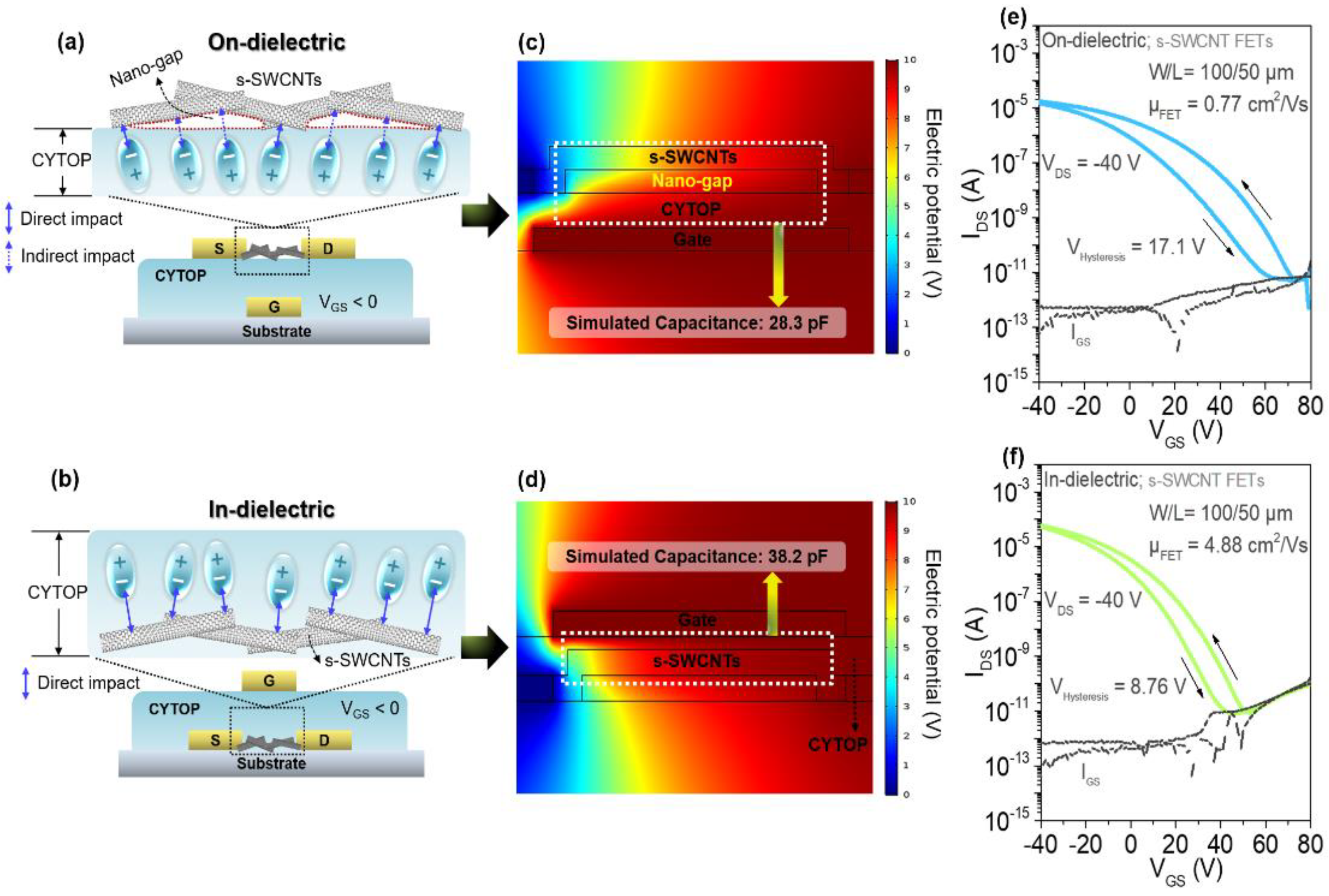
The structure of semiconductor/gate dielectric interface has a great influence on the electrical performance of SWCNT FETs, particularly with the staggered bottom-gate structure [
31,
32,
33]. This is mainly due to the stacking structure of the SWCNTs where the nanotubes are overlapped with each other. As a result, nano-gaps can be formed between the SWCNTs and the bottom gate dielectric layer, causing a weak gate-field applied to the SWCNTs [
34]. Meanwhile, using top-gate structure and soft gate dielectrics such as polymers and ion-gels, more intimate contacts between SWCNTs and gate dielectric can be made by conformally surrounding the SWCNTs with the soft gate dielectric [
35,
36,
37].
Accordingly, compared to the staggered bottom-gate structure, nano-gaps may be relatively suppressed by a structural feature of the top-gate structure. To evaluate the influence of using a soft gate dielectric on the electrical performance, both bottom-gate and top-gate structured s-SWCNT FETs were fabricated as shown in
Figure 3a,d using CYTOP as a gate dielectric, respectively. Here, the bottom-gate and top-gate FETs were designated as ‘on-dielectric’ and ‘in-dielectric’ structures depending on the position of SWCNTs in respect to the gate dielectric layer. Note that s-SWCNTs with the HAP treatment was used for this test. As shown in
Figure 3a, in the case of on-dielectric FETs, nano-gaps with the length of ~50 nm which is estimated by the AFM data exist between the SWCNTs and the gate dielectric, resulting in a weak gate-field and reduced charge accumulation. On the other hand, with the in-dielectric structure (
Figure 3d), the CYTOP gate dielectric conformably covers the SWCNTs and more effective charge accumulation can be possible. To verify the effect of FET structure on the charge accumulation, electrical simulations using the finite-element analysis (FEA) method were performed as shown in
Figure 3b,e (also,
Table S1). It was found that the top-gated in-dielectric device showed a higher capacitance (38.2 pF) compared to bottom-gated on-dielectric devices (28.3 pF) by the suppression of the nano-gaps. Following, SWCNT FETs with on-dielectric and in-dielectric structures were fabricated and their transfer characteristics were analyzed (
Figure S5). As shown in
Figure 3c,f, the in-dielectric structure FETs exhibited higher average field-effect mobility of 4.07 (standard deviation of 0.65 cm
2·V
−1·s
−1 ), and reduced hysteresis behavior (~8.76 V), which can be attributed to the higher number of holes accumulated in the s-SWCNT channel and the reduction of surface trap states caused by the air exposure.
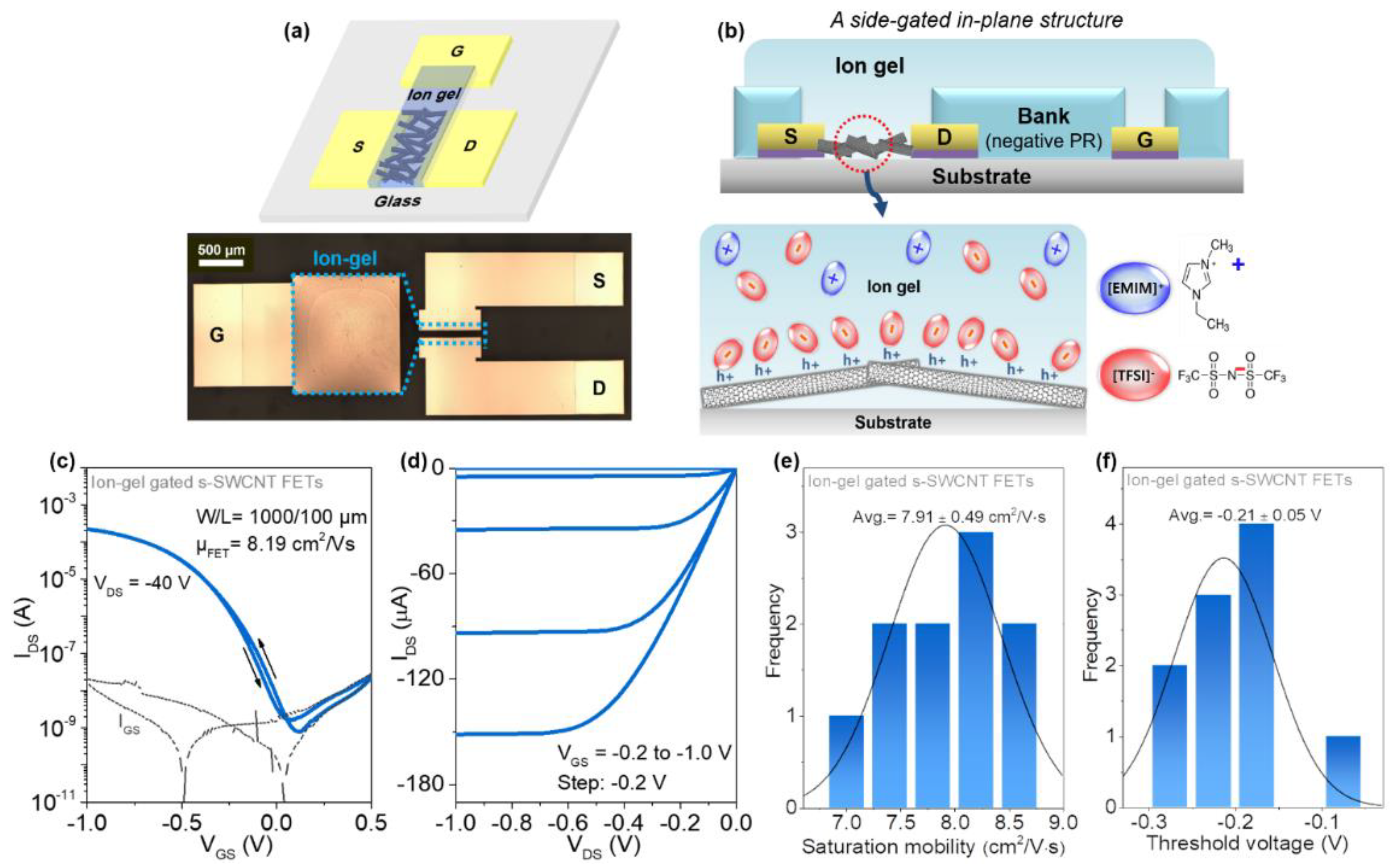
To further improve the electrical properties of SWCNT FETs and to realize a low-voltage operation, high-k ion-gel film was employed as a gate dielectric. Since the ion-gel gate dielectric can be fabricated at a low-temperature using a solution process similar to the CYTOP gate dielectric, SWCNT FETs with a top-gate-like structure can be fabricated as shown in
Figure 4a. In particular, after depositing the Cr/Au source/drain and gate electrodes, HAP-processed s-SWCNTs were spin-coated as a channel layer. Then, a negative photoresist was coated and patterned as a bank to isolate the ion-gel gate dielectric. Finally, an ion-gel solution consisting of 1-ethyl-3-methylimidazolium bis(trifluoro-methylsulfonyl) imide ([EMIM][TFSI]), polyethylene glycol diacrylate, and 2-hydroxy-2-methylpropiophenone was drop-casted at the bank region and photo-polymerized by UV exposure (
Figure 4b). When a negative gate voltage is applied, an electrical double layer (EDL) is formed at the s-SWCNT/ion-gel interface, inducing accumulation of positive hole charges in the s-SWCNT channel.
Figure 4c–f shows the transfer and output characteristics of the ion-gel-gated SWCNT FETs, respectively. The devices exhibited the improved electrical properties such as field-effect mobility of 8.19 cm
2·V
−1·s
−1 and current on/off ratio of ~10
5 and a low threshold voltage (V
th) of −0.2 V, attributing to the high capacitance of the ion-gel gate dielectric as well as the conformal contact between the ion-gel and the s-SWCNTs (
Figure 4).
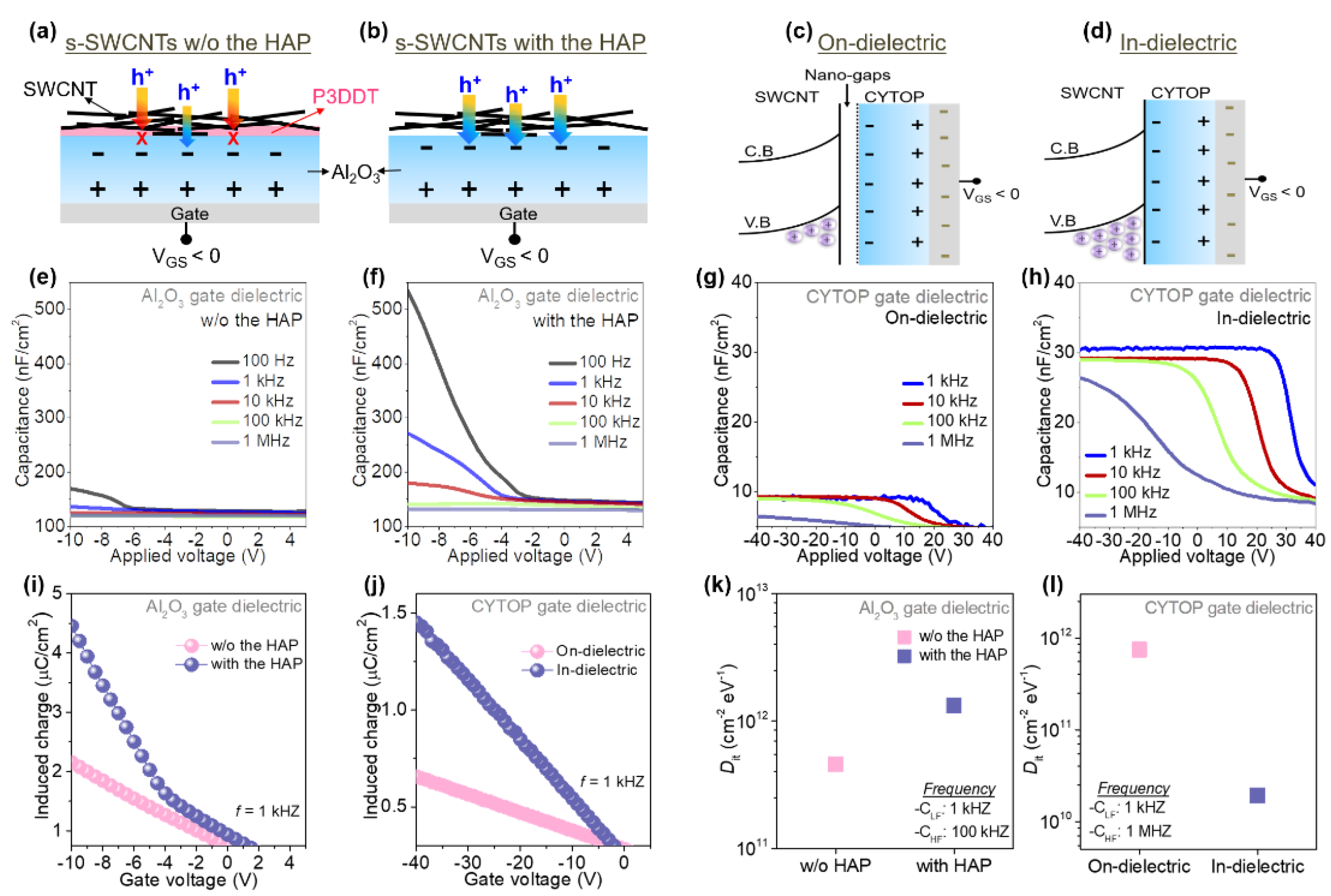
To further explain the variations of hole accumulation and transport properties depending on the HAP process and the device structure (on- or in-dielectric) with the gate dielectric materials (Al
2O
3, CYTOP, or ion-gel), schematics of the mechanism of gate modulation on hole-charge carriers in the s-SWCNT networks and the corresponding energy band diagram models were constructed as shown in
Figure 5a–d. Firstly, in the case of the SWCNT FETs on Al
2O
3 gate dielectric without the HAP treatment, hole-carriers can be accumulated near the Al
2O
3/s-SWCNT interface under a negative gate bias (V
GS < 0) to form a current pathway. As aforementioned, however, the charge carrier transport would be interrupted by the P3DDT polymer bound to s-SWCNTs which plays a role as a block-barrier for hole carriers. Additionally, the P3DDT may prevent gate-field from being induced charges at the interface, resulting in a small number of accumulating hole-carriers (
Figure 5a). On the other hand, as shown in
Figure 5b, the s-SWCNTs with the HAP treatment could lead to a number of charges induced by gate-field as well as enhance the charge-carrier transport due to the reduced P3DDT. However, it is noteworthy that compared to the s-SWCNT without the HAP treatment, a larger area of the s-SWCNT channel layer would be exposed to ambient gases by the reduction of P3DDT, causing a large hysteresis behavior, which is in agreement with the transfer curve of s-SWCNT TFTs with the HAP process (
Figure 2c). In addition to the effect of the HAP process on the electrical characteristics of the SWCNT FETs, device configurations significantly influence the entire properties of the TFTs.
Figure 5c and d shows the comparison of CYTOP on- and in-dielectric configurations for the accumulation of hole-carriers, respectively. In the case of CYTOP gate dielectric and on-dielectric device structure, nano-gaps exist between the s-SWCNT channel and the CYTOP as shown in
Figure 5c, causing reduced gate-field in the s-SWCNT channel and smaller number of accumulated holes. With the in-dielectric structure, however, the formation of the nano-gaps is suppressed by the conformal contact made between the CYTOP gate dielectric and the s-SWCNTs (
Figure 5d). Subsequently, more numbers of holes are accumulated in the channel layer resulting in improved field-effect mobility. Similarly, with the ion-gel gate dielectric and in-dielectric device structure (a side-gated in-plane structure), cations migrated to the s-SWCNT/ion-gel interface under a negative gate bias and relatively high number of holes can be accumulated in the s-SWCNT channel even at a low gate bias (
Figure S6a).
To verify the above the mechanisms and energy band models, capacitance-voltage (C-V) characteristics of metal-insulator-semiconductor (MIS) devices with Au/(Al
2O
3, CYTOP or ion-gel)/s-SWCNTs structures were analyzed. As shown in
Figure 5e–h, in all cases, the number of accumulated hole carriers increased with negative gate biasing. Additionally, the capacitance value was significantly decreased with the applied frequency. The increase of capacitance at low frequency is attributed to the interface states that cannot respond quickly. In contrary, at the low frequency, the charges can follow the ac signal easily and the interface state capacitance can be considered to the total capacitance. The C-V characteristics were largely varied with the presence of P3DDT in the s-SWCNT channel. Particularly, with the HAP-processed s-SWCNTs, higher capacitance value was obtained compared to the s-SWCNTs with P3DDT (
Figure 5e,f). As described, compared to the pristine s-SWCNTs without the HAP treatment, the s-SWCNTs with the HAP treatment could be exposed to air through the reduced P3DDT bound to s-SWCNT, resulting in higher area capacitance. This result is due to an increase in the effective contact area between s-SWCNTs and gate dielectric. However, despite such positive features, the reduction of the P3DDT would negatively affect a hysteresis of the SWCNT FETs due to the direct adsorption of water molecules on the s-SWCNT surfaces, which is in tune with the hysteresis characteristic of HAP-processed SWCNT FETs. In addition, the device configuration has a significant impact on the C-V characteristics. As shown in
Figure 5g,h, with the in-dielectric FET structure completely covering the s-SWCNTs with the CYTOP gate dielectric, the capacitance value was increased in all frequency domains compared to the on-dielectric device, supporting the elimination of the nano-gaps. Additionally, the ion-gel gated s-SWCNTs showed a similar trend to the in-dielectric structure and the highest areal capacitance value (~50 µF·cm
−2) due to a high-k ion-gel film (
Figure S6b,c).
Additionally, from the C-V characteristics, we extracted the induced charge density (Q
ind) in the s-SWCNT channel layer using the following Equation (1) [
35,
38],
where C
GD and V
th are the areal capacitance of gate dielectric and the threshold voltage in the linear region, respectively. As a result, both the HAP process reducing the P3DDT polymer, and the in-dielectric device structure providing the conformal contact at the interface improved the Q
ind, resulting in a lot of the accumulated hole carriers and the enhanced charge transport of the s-SWCNT (
Figure 5i,k). Additionally, for further analysis of the interface between the s-SWCNT and gate dielectric, the interface trap density (D
it) has been investigated from the C-V characteristics using the Equation (2) below [
38,
39],
where C
LF, C
HF, C
di, and q are the low-frequency, high-frequency, gate dielectric capacitance, and electron charge, respectively. The results indicate that the interface trap density considerably increased as the P3DDT polymers bonded with the s-SWCNTs were reduced by the HAP process, as shown in
Figure 5j. It means that a clean s-SWCNT surface with the reduced P3DDT can lead to active adsorption of water molecules, causing a larger hysteresis behavior. Therefore, it is important to reduce D
it, which degrades electrical performance.
Figure 5i shows the comparison of the D
it depending on device configuration (on- and in-dielectric). As expected, with the in-dielectric configuration covering the entire s-SWCNT channel layer, the D
it decreased considerably. This result is attributed to both a conformal/imitate contact mitigating nano-gaps that can interrupt inducible charges at the interface and the passivation effect that can prevent the absorption of ambient molecules on the s-SWCNT channel surface. Similarly, for the ion-gel gated s-SWCNTs FETs, the interface trap density would be positively relieved due to more conformal contact with an ion-gel dielectric.


 and
and 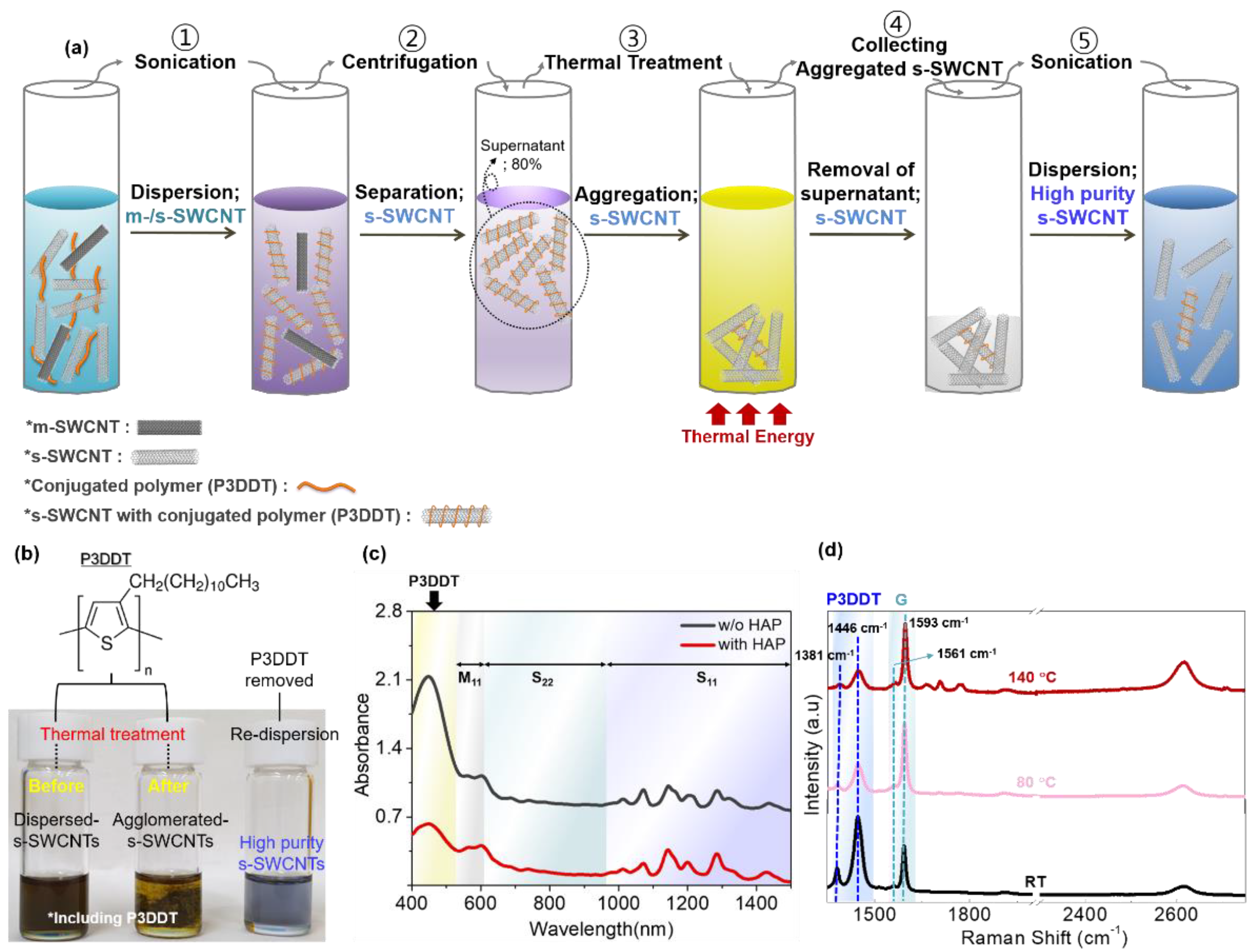


