
Dye-Sensitized Solar Cell for Building-Integrated Photovoltaic (BIPV) Applications


 ,
,  ,
,
Abstract
:1. Introduction
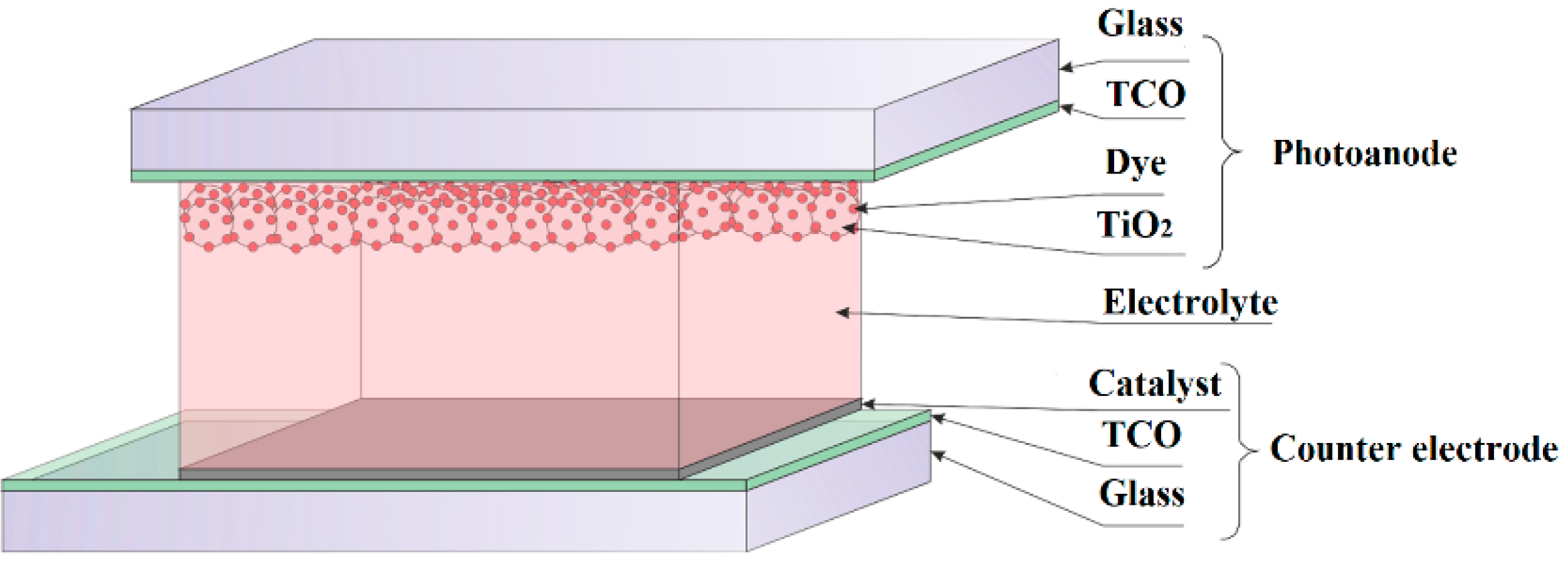
2. Material Descriptions and Research Methodology
2.1. Substrates Modification
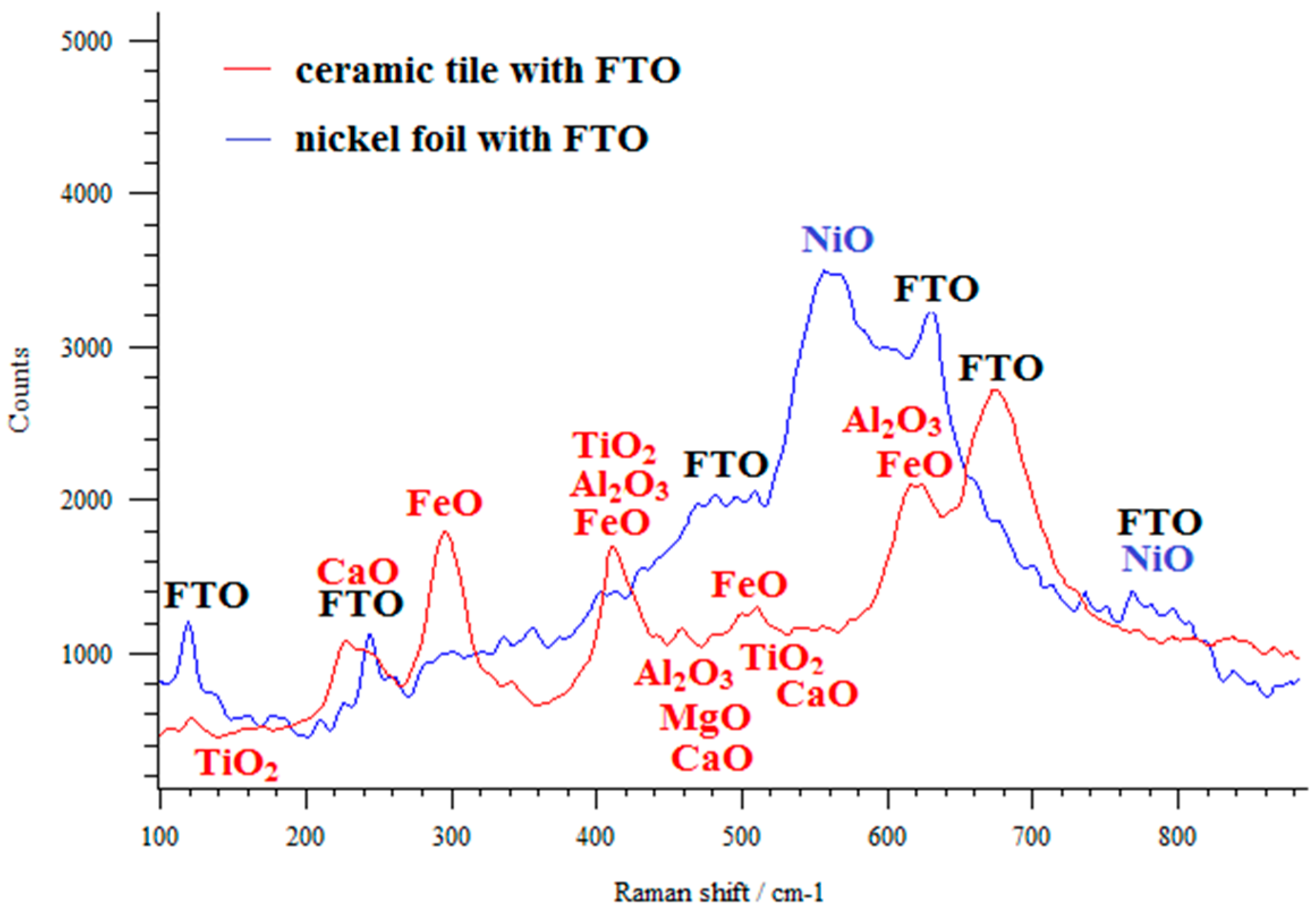
2.2. Characterization Methods
2.3. Device Fabrication and Characterization
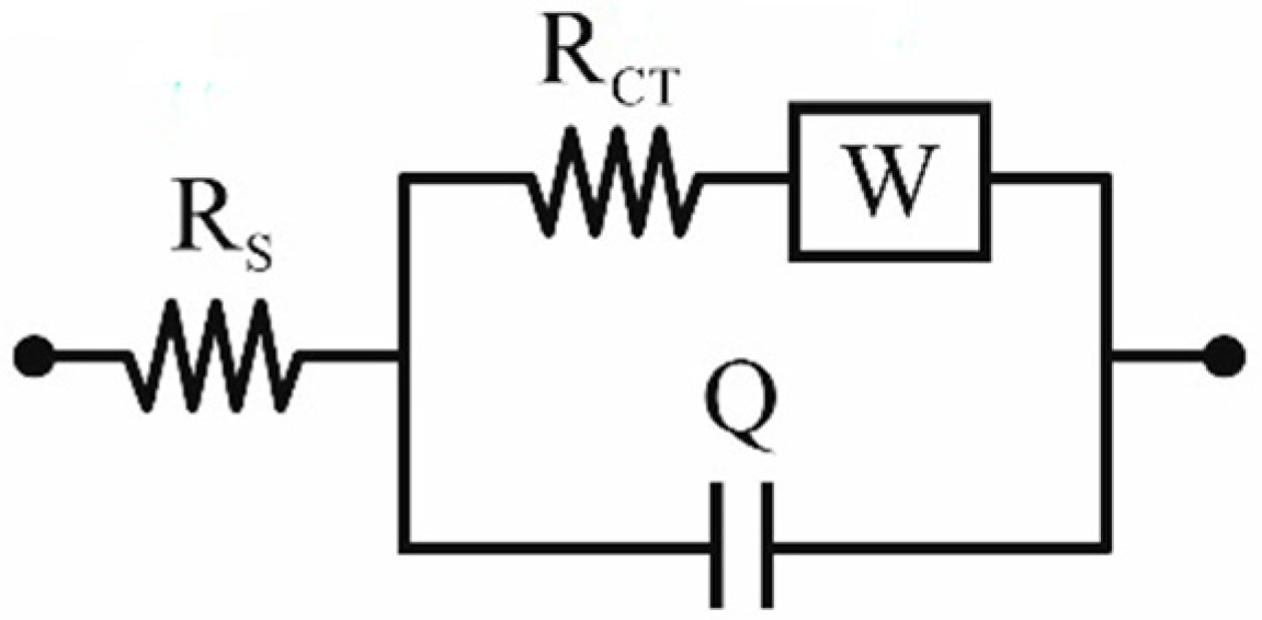
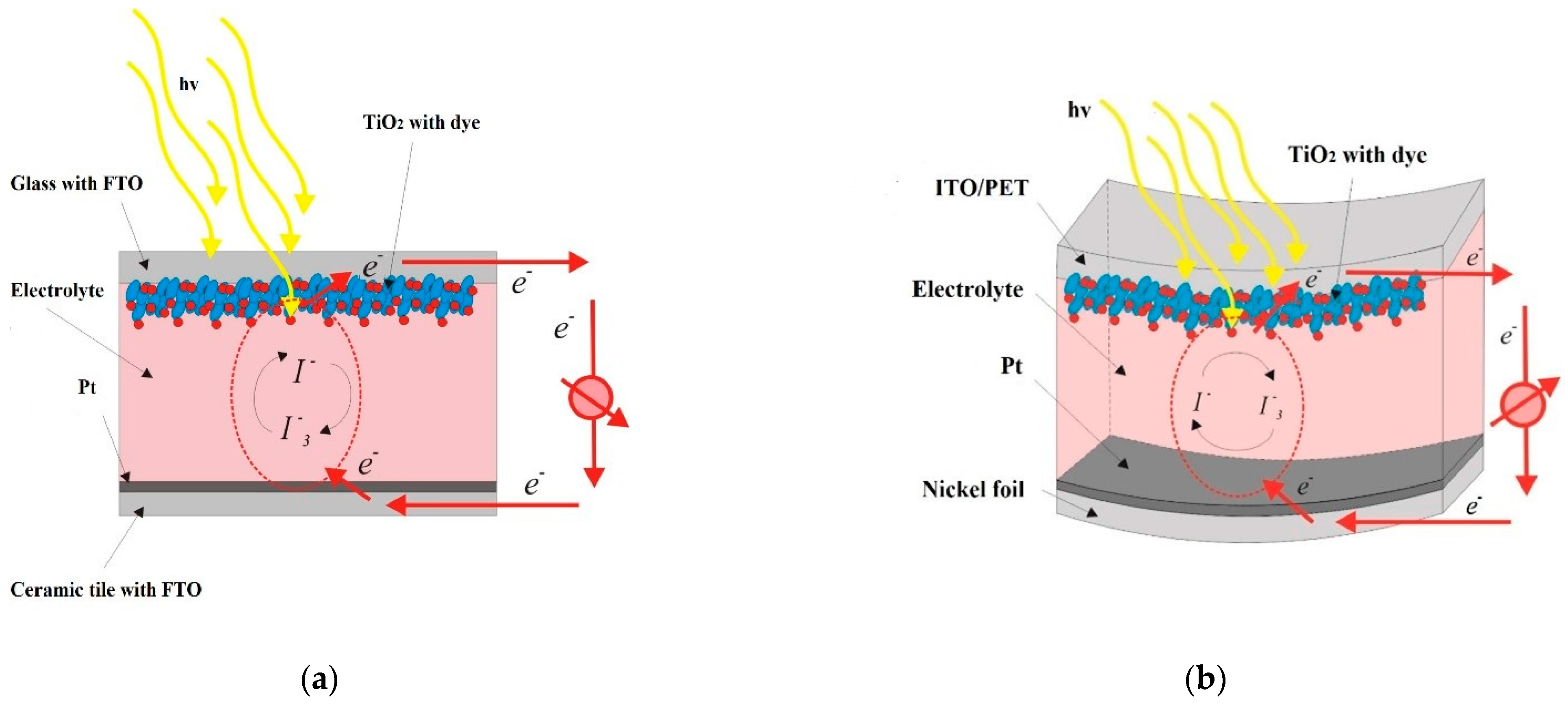
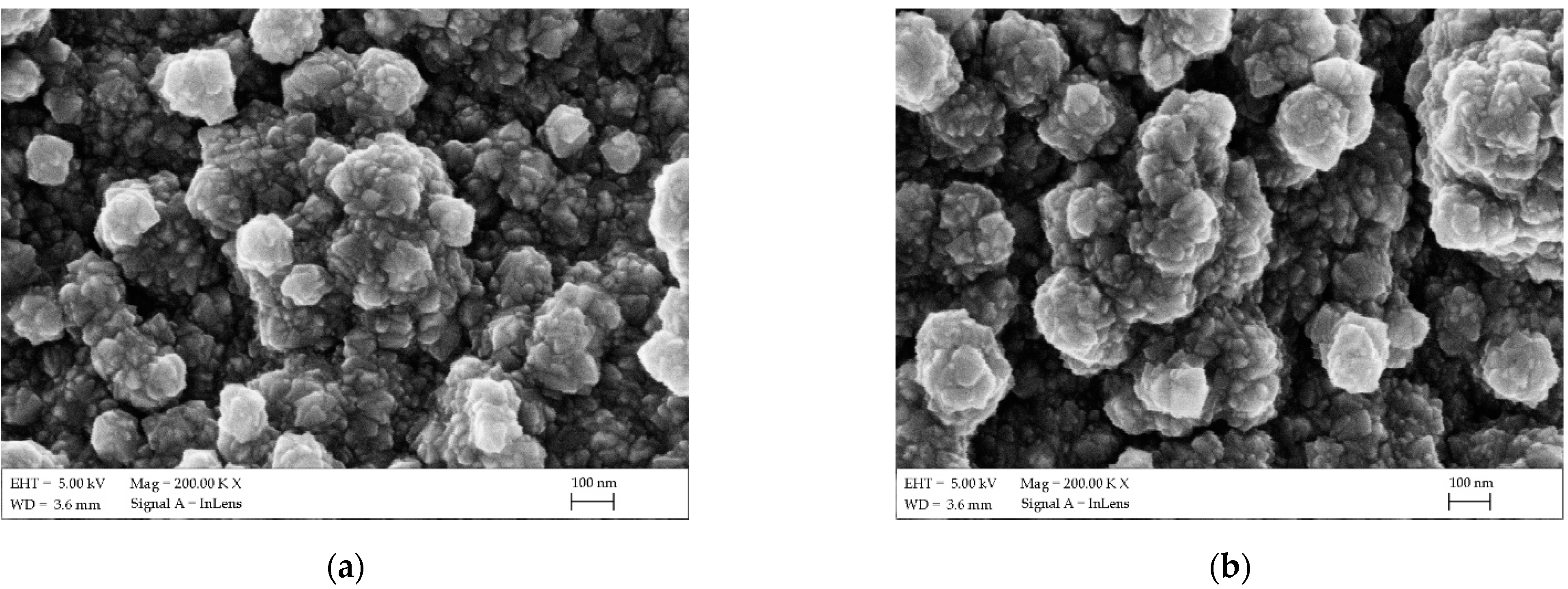
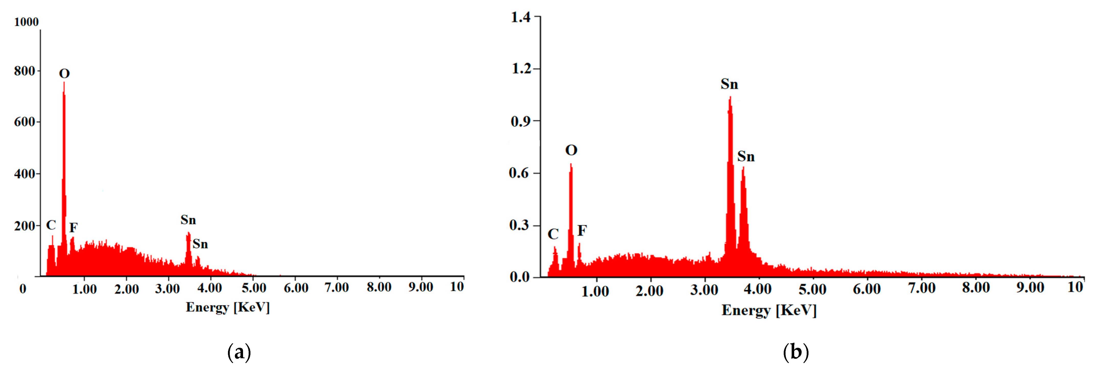
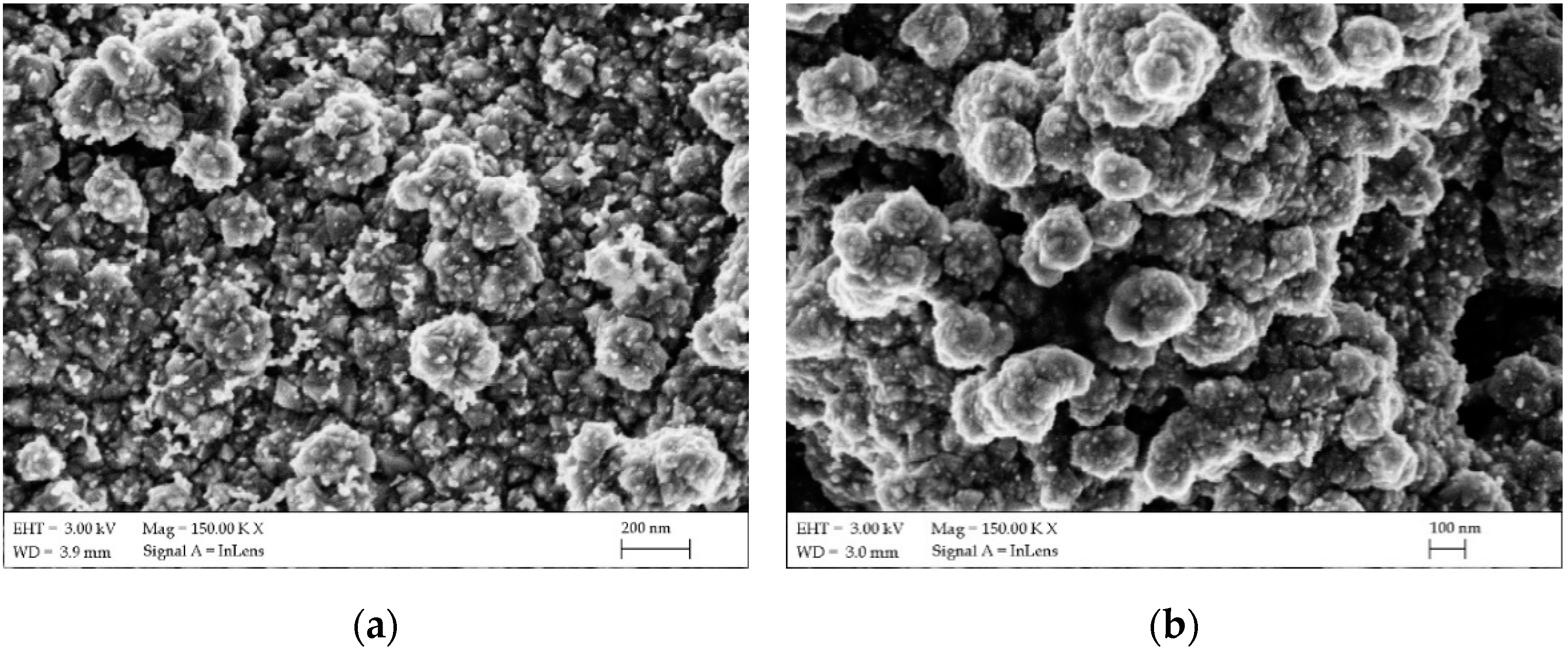
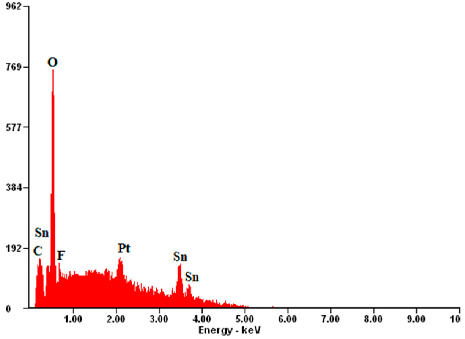
3. Results and Discussion
4. Conclusions
Author Contributions
Funding
Institutional Review Board Statement
Informed Consent Statement
Data Availability Statement
Acknowledgments
Conflicts of Interest
References
- Battaglia, C.; Cuevas, A.; De Wolf, S. High-efficiency crystalline silicon solar cells: Status and perspectives. Energy Environ. Sci. 2016, 9, 1552–1576. [Google Scholar] [CrossRef] [Green Version]
- Masuko, K.; Shigematsu, M.; Hashiguchi, T.; Fujishima, D.; Kai, M.; Yoshimura, N.; Yamaguchi, T.; Ichihashi, Y.; Mishima, T.; Matsubara, N.; et al. Achievement of More Than 25% Conversion Efficiency with Crystalline Silicon Heterojunction Solar Cell. IEEE J. Photovolt. 2014, 4, 1433–1435. [Google Scholar] [CrossRef]
- Deng, S.; Wang, R.; Dai, Y. How to evaluate performance of net zero energy building—A literature research. Energy 2014, 71, 1–16. [Google Scholar] [CrossRef]
- De Santoli, L. Guidelines on energy efficiency of cultural heritage. Energy Build. 2015, 86, 534–540. [Google Scholar] [CrossRef]
- Heinstein, P.; Ballif, C.; Perret-Aebi, L.-E.E. Building integrated photovoltaics (BIPV): Review, potentials, barriers and myths. Green 2013, 3, 125–156. [Google Scholar] [CrossRef]
- Jelle, B.P.; Breivik, C.; Røkenes, H.D. Building integrated photovoltaic products: A state-of-the-art review and future research opportunities. Sol. Energy Mater. Sol. Cells 2012, 100, 69–96. [Google Scholar] [CrossRef] [Green Version]
- Huang, Y.-C.; Chan, C.C.; Wang, S.-J.; Lee, S.-K. Development of building integrated photovoltaic (BIPV) system with PV ceramic tile and its application for building façade. Energy Procedia 2014, 61, 1874–1878. [Google Scholar] [CrossRef] [Green Version]
- Debbarma, M.; Sudhakar, K.; Baredar, P. Comparison of BIPV and BIPVT: A review. Resour. Effic. Technol. 2017, 3, 263–271. [Google Scholar] [CrossRef]
- O’Regan, B.; Grätzel, M. A low-cost, high-efficiency solar cell based on dye-sensitized colloidal TiO2 films. Nature 1991, 353, 737–740. [Google Scholar] [CrossRef]
- Ferber, J.; Stangl, R.; Luther, J. An electrical model of the dye-sensitized solar cell. Sol. Energy Mater. Sol. Cells 1998, 53, 29–54. [Google Scholar] [CrossRef]
- Liang, M.; Chen, J. Arylamine organic dyes for dye-sensitized solar cells. Chem. Soc. Rev. 2013, 42, 3453. [Google Scholar] [CrossRef] [PubMed]
- Ezhov, A.; Zhdanova, K.A.; Bragina, N.A.; Mironov, A.F. Approaches to Improve Efficiency of Dye-Sensitized Solar Cells. Macroheterocycles 2016, 9, 337–352. [Google Scholar] [CrossRef] [Green Version]
- Yang, J.; Ganesan, P.; Teuscher, J.; Moehl, T.; Kim, Y.J.; Yi, C.; Comte, P.; Pei, K.; Holcombe, T.W.; Nazeeruddin, M.K.; et al. Influence of the Donor Size in D−π–A Organic Dyes for Dye-Sensitized Solar Cells. J. Am. Chem. Soc. 2014, 136, 5722–5730. [Google Scholar] [CrossRef] [PubMed]
- Li, Y.; Li, Y.; Song, P.; Ma, F.; Liang, J.; Sun, M. Screening and design of high-performance indoline-based dyes for DSSCs. RSC Adv. 2017, 7, 20520–20536. [Google Scholar] [CrossRef] [Green Version]
- Bella, F.; Galliano, S.; Gerbaldi, C.; Viscardi, G. Cobalt-Based Electrolytes for Dye-Sensitized Solar Cells: Recent Advances towards Stable Devices. Energies 2016, 9, 384. [Google Scholar] [CrossRef] [Green Version]
- Raj, A.C.; Prasanth, R. A critical review of recent developments in nanomaterials for photoelectrodes in dye-sensitized solar cells. J. Power Sources 2016, 317, 120–132. [Google Scholar] [CrossRef]
- Gerosa, M.; Sacco, A.; Scalia, A.; Bella, F.; Chiodoni, A.; Quaglio, M.; Tresso, E.; Bianco, S. Toward Totally Flexible Dye-Sensitized Solar Cells Based on Titanium Grids and Polymeric Electrolyte. IEEE J. Photovolt. 2016, 6, 498–505. [Google Scholar] [CrossRef]
- Milan, R.; Selopal, G.S.; Epifani, M.; Natile, M.M.; Sberveglieri, G.; Vomiero, A.; Concina, I. ZnO/SnO2 engineered composite photoanodes for dye-sensitized solar cells. Sci. Rep. 2015, 5, 14523. [Google Scholar] [CrossRef] [Green Version]
- Clifford, J.N.; Palomares, E.; Nazeeruddin, K.; Grätzel, M.; Nelson, J.; Li, X.; Long, A.N.J.; Durrant, J.R. Molecular Control of Recombination Dynamics in Dye-Sensitized Nanocrystalline TiO2Films: Free Energy vs Distance Dependence. J. Am. Chem. Soc. 2004, 126, 5225–5233. [Google Scholar] [CrossRef]
- Shimada, K.; Toyoda, T.; Shahiduzzaman, M.; Taima, T. Platinum counter electrodes for dye-sensitized solar cells prepared by one-step dipping process. Jpn. J. Appl. Phys. 2019, 58, 1–4. [Google Scholar] [CrossRef]
- Yu-Hsun, N.; Chen, H.-H.; Hsu, H.-H.; Rangasamy, M.; Hu, G.-M.; Yong, Z.-R.; Kuo, P.-Y.; Chou, J.-C.; Lai, C.-H.; Ko, C.-C.; et al. Study of How Photoelectrodes Modified by TiO2/Ag Nanofibers in Various Structures Enhance the Efficiency of Dye-Sensitized Solar Cells under Low Illumination. Energies 2020, 13, 1–14. [Google Scholar]
- Dao, V.-D.; Tran, C.Q.; Ko, S.-H.; Choi, H.-S. Dry plasma reduction to synthesize supported platinum nanoparticles for flexible dye-sensitized solar cells. J. Mater. Chem. A 2013, 1, 4436. [Google Scholar] [CrossRef]
- Dang, H.-L.T.; Dao, V.-D.; Vu, N.H.; Quang, D.V.; Vu, H.H.T.; Nguyen, T.H.; Mohamed, I.M.; Hoang, X.-C.; Vu, D.A.; Tuan, P.A. Balance between the explored Pt counter electrode in an electrolyte medium and the photoanode for highly efficient liquid-junction photovoltaic devices. J. Sci. Adv. Mater. Devices 2020, 5, 180–184. [Google Scholar] [CrossRef]
- Baiju, K.G.; Murali, B.; Rao, R.S.; Jayanarayanan, K.; Kumaresan, D. Heat sink assisted elevated temperature sintering process of TiO2 on polymer substrates for producing high performance flexible dye-sensitized solar cells. Chem. Eng. Process. Process. Intensif. 2020, 149, 107817. [Google Scholar] [CrossRef]
- Weerasinghea, H.C.; Huanga, F.; Chenga, Y.-B. Fabrication of flexible dye sensitized solar cells on plastic substrates. Nano Energy 2013, 2, 174–189. [Google Scholar] [CrossRef]
- Sheng, L.; Li, G.; Zhang, W.; Wang, K. Full-stainless steel mesh dye-sensitized solar cells based on core-shell ZnO/TiO2 nanorods. Optik 2019, 184, 90–97. [Google Scholar] [CrossRef]
- Toivola, M.; Ahlskog, F.; Lund, P. Industrial sheet metals for nanocrystalline dye-sensitized solar cell structures. Sol. Energy Mater. Sol. Cells 2006, 90, 2881–2893. [Google Scholar] [CrossRef]
- Kanta, A.-F.; Decroly, A. Stainless steel electrode characterizations by electrochemical impedance spectroscopy for dye sensitized solar cells. Electrochim. Acta 2011, 56, 10276–10282. [Google Scholar] [CrossRef]
- Ouyang, F.Y.; Tai, W.L. Enhanced corrosion resistance of TiN-coated stainless steels for the application in flexible dye-sensitized solar cells. Appl. Surf. Sci. 2013, 276, 563–570. [Google Scholar] [CrossRef]
- Wang, B.; Kerr, L.L. Dye sensitized solar cells on paper substrates. Sol. Energy Mater. Sol. Cells 2011, 95, 2531–2535. [Google Scholar] [CrossRef]
- Kumara, G.; Ranasinghe, S.; Jayaweera, E.N.; Bandara, H.M.N.; Okuya, M.; Rajapakse, R.M.G. Preparation of Fluoride-Doped Tin Oxide Films on Soda–Lime Glass Substrates by Atomized Spray Pyrolysis Technique and Their Subsequent Use in Dye-Sensitized Solar Cells. J. Phys. Chem. C 2014, 118, 16479–16485. [Google Scholar] [CrossRef]
- Banyamin, Z.Y.; Kelly, P.J.; West, G.; Boardman, J. Electrical and Optical Properties of Fluorine Doped Tin Oxide Thin Films Prepared by Magnetron Sputtering. Coatings 2014, 4, 732–746. [Google Scholar] [CrossRef]
- Kim, C.Y.; Riu, D.H. Raman scattering, electrical and optical properties of fluorine-doped tin oxide thin films with (200) and (301) preferred orientation. Mater. Chem. Phys. 2014, 148/3, 810–817. [Google Scholar] [CrossRef]
- Dobrzański, L.A.; Szindler, M.; Prokopowicz, M.P.V.; Drygała, A.; Lukaszkowicz, K.; Jung, T.; Szindler, M.M. Transparent platinum counter electrode for dye-sensitized solar cells. J. Achiev. Mater. Manuf. Eng. 2015, 68/1, 5–10. [Google Scholar]
- Dao, V.-D.; Kim, S.-H.; Choi, H.-S.; Kim, J.-H.; Park, H.-O.; Lee, J.-K. Efficiency Enhancement of Dye-Sensitized Solar Cell Using Pt Hollow Sphere Counter Electrode. J. Phys. Chem. C 2011, 115, 25529–25534. [Google Scholar] [CrossRef]


| FTO Samples | ρ [Ω·cm] | n [cm−3] | µ [cm2/V·s] |
|---|---|---|---|
| Nickel foil (non heated) | 1.23 × 10⁻⁴ | 2.68 × 10²¹ | 24.20 |
| Nickel foil (Heated = 100 °C) | 5.69 × 10⁻⁵ | 4.52 × 10²¹ | 24.30 |
| Ceramic tile (non heated) | 1.26 × 10⁻⁴ | 2.71 × 10²¹ | 24.10 |
| Ceramic tile (Heated = 100 °C) | 5.76 × 10⁻⁵ | 4.54 × 10²¹ | 24.30 |
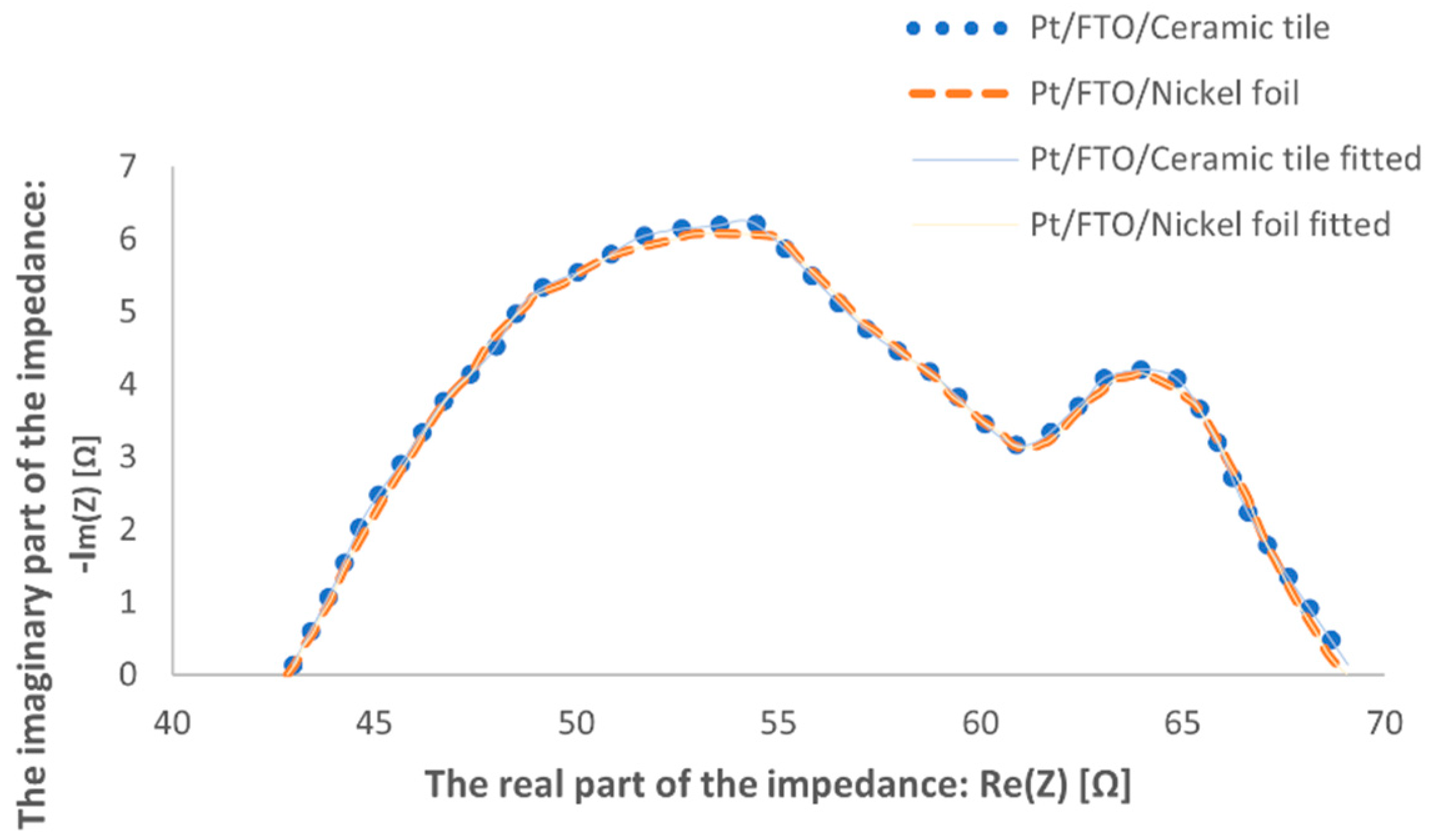
| Pt Samples | Rct [Ω] | Rs [Ω] |
|---|---|---|
| Nickel foil | 26.5 | 42.5 |
| Ceramic tile | 27.3 | 41.8 |
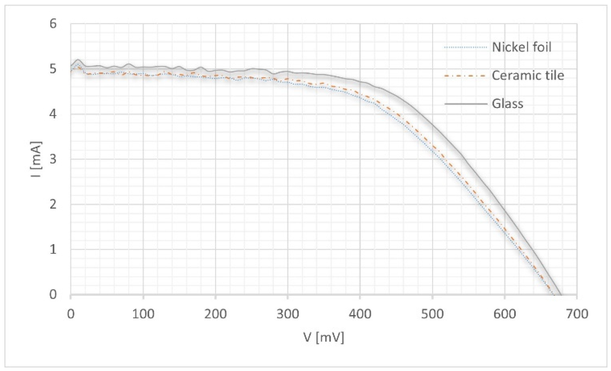
| DSSC Sample | Active Area [cm2] | Jsc [mA/cm2] | Isc [mA] | Voc [mV] | Imax [mA] | Vmax [mV] | Pmax [mW] | FF | Eff [%] |
|---|---|---|---|---|---|---|---|---|---|
| Nickel foil | 0.4 | 12.40 | 4.959 | 667.453 | 4.157 | 425.694 | 1.769 | 0.53 | 4.34 |
| Ceramic tile | 0.4 | 12.36 | 4.944 | 668.392 | 4.215 | 431.203 | 1.818 | 0.55 | 4.48 |
| Glass | 0.4 | 12.68 | 5.072 | 677.769 | 4.395 | 450.470 | 1.980 | 0.58 | 4.83 |
Publisher’s Note: MDPI stays neutral with regard to jurisdictional claims in published maps and institutional affiliations. |
© 2021 by the authors. Licensee MDPI, Basel, Switzerland. This article is an open access article distributed under the terms and conditions of the Creative Commons Attribution (CC BY) license (https://creativecommons.org/licenses/by/4.0/).
Share and Cite
Szindler, M.; Szindler, M.; Drygała, A.; Lukaszkowicz, K.; Kaim, P.; Pietruszka, R. Dye-Sensitized Solar Cell for Building-Integrated Photovoltaic (BIPV) Applications. Materials 2021, 14, 3743. https://doi.org/10.3390/ma14133743
Szindler M, Szindler M, Drygała A, Lukaszkowicz K, Kaim P, Pietruszka R. Dye-Sensitized Solar Cell for Building-Integrated Photovoltaic (BIPV) Applications. Materials. 2021; 14(13):3743. https://doi.org/10.3390/ma14133743
Chicago/Turabian StyleSzindler, Marek, Magdalena Szindler, Aleksandra Drygała, Krzysztof Lukaszkowicz, Paulina Kaim, and Rafał Pietruszka. 2021. "Dye-Sensitized Solar Cell for Building-Integrated Photovoltaic (BIPV) Applications" Materials 14, no. 13: 3743. https://doi.org/10.3390/ma14133743
APA StyleSzindler, M., Szindler, M., Drygała, A., Lukaszkowicz, K., Kaim, P., & Pietruszka, R. (2021). Dye-Sensitized Solar Cell for Building-Integrated Photovoltaic (BIPV) Applications. Materials, 14(13), 3743. https://doi.org/10.3390/ma14133743