Article

Low-Temperature Metallization and Laser Trimming Process for Microwave Dielectric Ceramic Filters

1
Department of Electrical Engineering, National Changhua University of Education, Changhua 500, Taiwan
2
Mechanical and System Research Laboratories, Industrial Technology and Research Institute, Hsinchu 310, Taiwan
*
Author to whom correspondence should be addressed.
Materials 2021, 14(24), 7519; https://doi.org/10.3390/ma14247519
Submission received: 14 November 2021 / Revised: 6 December 2021 / Accepted: 6 December 2021 / Published: 8 December 2021
(This article belongs to the Special Issue Materials for LTCC Technology)

Abstract

:
This paper describes a low-temperature metallization and laser trimming process for microwave dielectric ceramic filters. The ceramic was metalized by electroless copper plating at a temperature lower than those of conventional low-temperature co-fired ceramic (LTCC) and direct bond copper (DBC) methods. Compared with filters made via traditional silver paste sintering, the metal in the holes of the microwave dielectric filters is uniform, smooth, and does not cause clogging nor become detached. Further, the batches of fabricated filters do not require individual inspection, reducing energy, labor, cost, and time requirements. A microwave dielectric filter was then manufactured from the prepared ceramic using a laser trimming machine with a line width and position error within ±50 μm; this demonstrates a more accurately controlled line width than that offered by screen printing. After using HFSS software simulations for preliminary experiments, the microwave dielectric filter was tuned to a target Wi-Fi band of 5.15–5.33 GHz; the return loss was <−10 dB, and the insertion loss was >−3 dB. To implement the real-world process, the laser parameters were optimized. Laser trimming has a higher success rate than traditional manual trimming, and the microwave dielectric filter manufactured here verified the feasibility of this process.

1. Introduction

Microwave dielectric ceramics are widely applied in many fields, such as mobile communications, wireless local networks, and satellite positioning and communications. Microwave dielectric ceramics with high dielectric constants and low loss tangents are suitable for devices such as filters, oscillators, and antennas [1,2,3]. The MgTiO3-CaTiO3 used in this study is a dielectric ceramic material that is widely used in microwave applications. The MgTiO3-CaTiO3 [4,5,6,7] has the desired properties for making compact and low-loss microwave devices, viz. a high dielectric constant (Dk), high quality factor/low loss (Q × f), and low-temperature coefficients of dielectric constant (TCK). Table 1 summarizes the properties of some MgTiO3-CaTiO3 materials.
As the market for and volume of microwave dielectric ceramics grow continuously, processes that consume less power and time have been investigated globally [8,9,10]. For instance, novel low-temperature processes for microwave dielectric ceramic metallization have been proposed [11,12,13], including an electroless copper plating strategy previously developed by our group [13]. The temperature at which our previously fabricated metallization process operates is less than 50 °C; this avoids requirements of increasing and decreasing temperature, which saves both energy and time, respectively. Another benefit of this low-temperature process is that it results in metal with uniform and smooth thicknesses and other dimensions; this provides cross sections superior to those of conventional low-temperature co-fired ceramics (LTCCs), which are often clogged by incompletely attached metal (Figure 1).
A manufactured microwave dielectric ceramic filter with four through-holes is shown in Figure 1a; the through-holes were drilled using a laser. Figure 1b,c show the cross sections (along the dashed line shown in Figure 1a) of filters prepared with the conventional LTCC process and the low-temperature metallization process, respectively. Figure 1b,c show that the metal thickness and dimensions provided by the low-temperature metallization process are more uniform and smoother than those provided by the conventional LTCC process, which would avoid the metal clog problems associated with the traditional process. Furthermore, the batches of microwave dielectric filters do not need to be inspected separately, which saves energy, labor, cost, and time.
After the low-temperature metallization process, the frequency response band of the microwave dielectric ceramic filter was lower than the target specifications. Hence, a laser trimming process was introduced to modify the ceramic structure to shift the frequency response to the desired band. The low-temperature metallization and laser trimming process of the microwave dielectric ceramic filter are explained in Section 2. In Section 3, an electromagnetic 3D simulation software is used to understand the characteristic moving trend of the microwave dielectric ceramic filter after applying the laser trimming process. In Section 4, the laser trimming process is applied to real ceramic samples to determine the associations between the laser trimming parameter recipe and the digging depth. After a series of processes and testings, optimized laser trimming parameter recipes were obtained. In Section 5, the final process and measurement results are presented. This study is concluded in Section 6.

2. Low-Temperature Metallization Process and Filter Specification

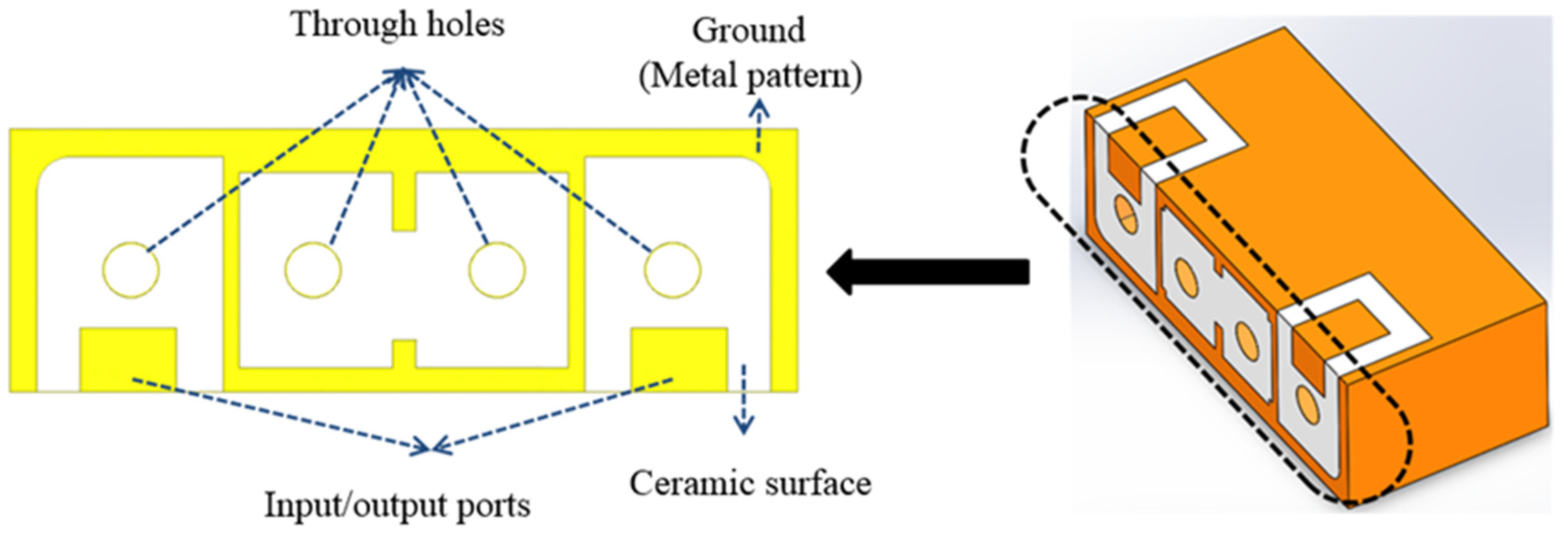
The structure of the microwave dielectric ceramic filter is shown in Figure 2.
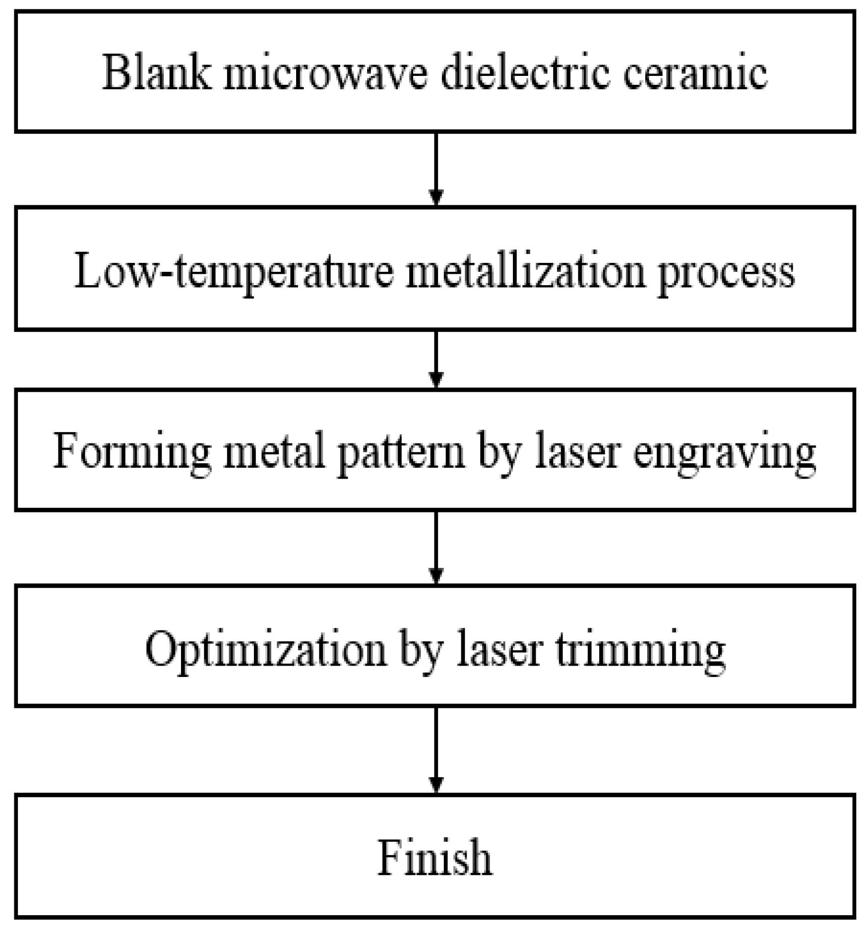
There are four through-holes with metal on the inner walls and a designated metal pattern on the ceramic surface. The dimensions were approximately 8 × 3 × 4 mm3. The low-temperature metallization and laser trimming processes are shown in Figure 3.
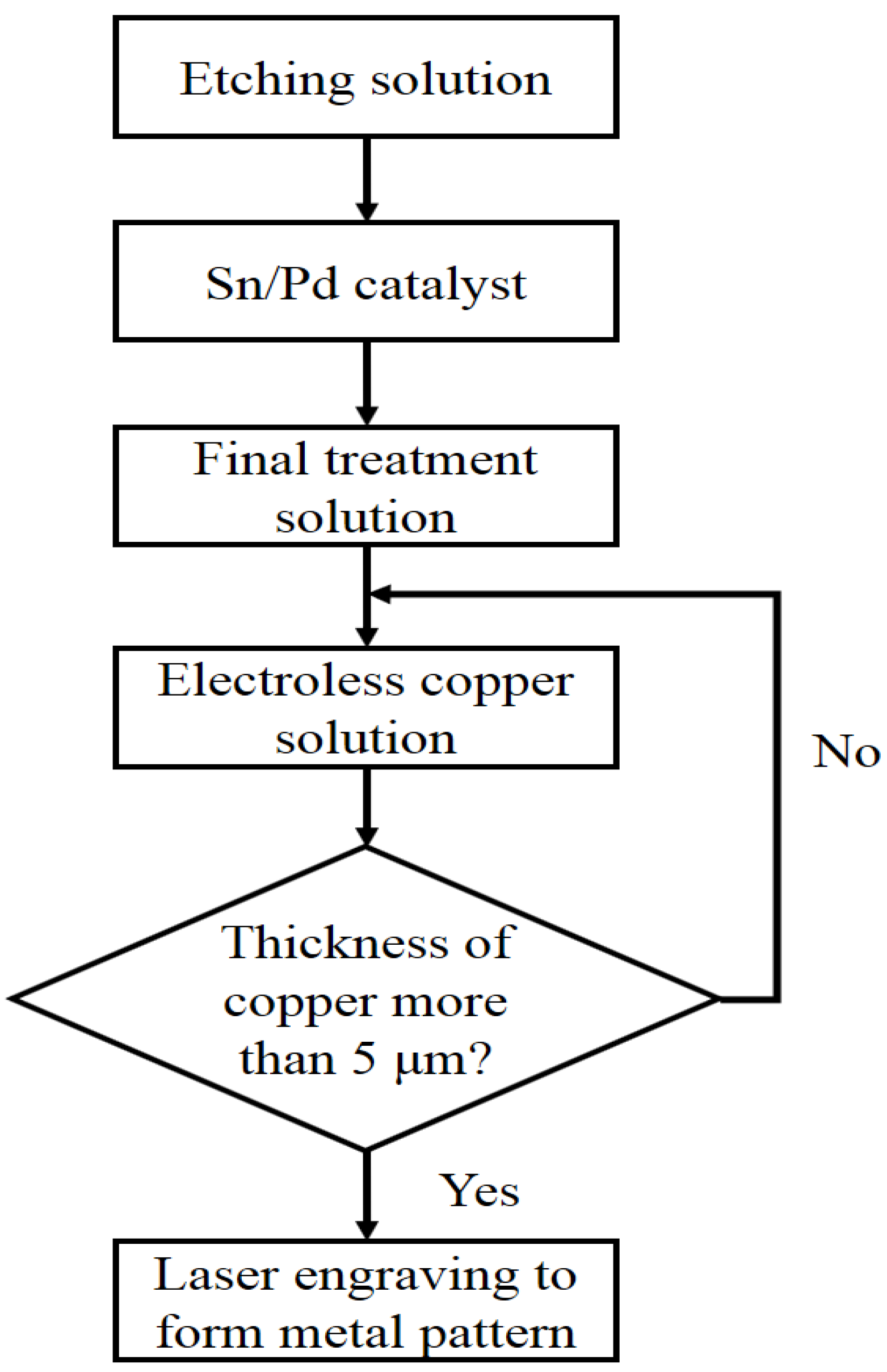
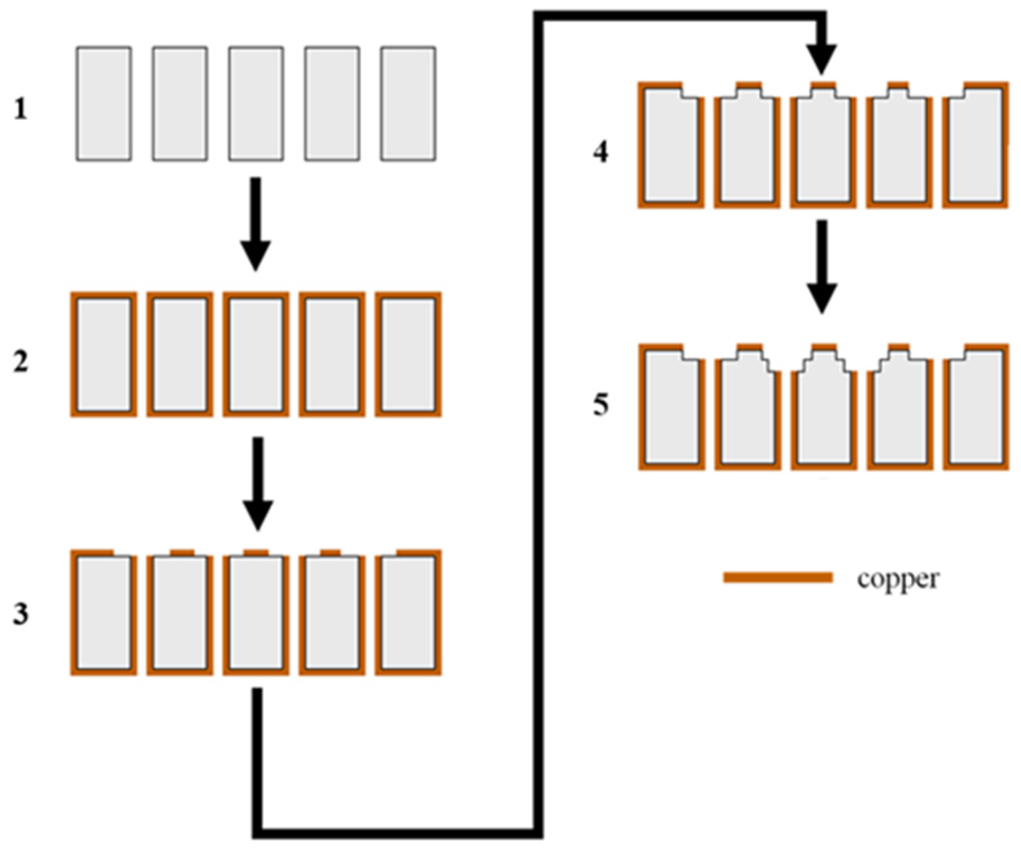
First, a blank microwave dielectric ceramic with the desired dimensions was obtained. The microwave dielectric ceramic metallization technology involves processing the microwave dielectric ceramic surface and depositing a copper metal on it using electroless copper plating technology; the detailed steps are shown in Figure 4 [13].
To form micro-pores on the surfaces of the ceramics and their holes, the CaTiO3 component was dissolved and removed from the ceramic using an oxidative etching solution; (e.g., phosphoric acid and HCl). After five minutes in the etching solution, the solution color was relatively yellow, which suggests that the Ca/Ti particles dissolved in the solution. The etching solution roughens the ceramic surface, which helps metals to adhere to it. The ceramic was then kept in an activator for ten minutes; the activator contained Sn and Pd ions that adhered to the ceramic surface. The ceramic was kept in the cleaning agent for three minutes as a final treatment to remove any free Sn particles, leaving just the Sn ions on the surface. Finally, the ceramic was placed in a copper solution that was heated with a water bath for one hour, where the temperature was maintained between 40 and 50 °C to control the deposition rate at approximately 5–7 µm/h. If the temperature is lower than 40 °C, the process may be too slow; if the temperature is higher than 50 °C, the process may be too fast, which could cause uneven copper thickness and poor copper adhesion. Owing to this being a low-temperature technology and the process being rapid, this metallization method has high energy-saving benefits. The desired metal pattern was then formed by laser engraving. For this, the width and position of the circuit were accurately controlled with a minimum line width of less than 50 μm, and the position accuracy was controlled within ±50 μm. These first three steps were introduced in previous works [11,12,13].
The characteristics of the manufactured microwave dielectric ceramic filters differed from the specifications, as shown in Table 2.
The target passband is between 5.15 and 5.33 GHz; this targets a 5-GHz Wi-Fi application with channel numbers from 32 to 64. The input matching (S11) should be less than −10 dB and the in-band loss (S21) should be higher than −3 dB at 5.15 to 5.33 GHz. Note that fL and fH represent the lowest and highest frequencies, respectively, with S11 being less than −10 dB. The passband bandwidth (BW) is the difference between fL and fH, and the image rejection (S21) should be less than −60 dB at ~5.5 GHz. This aims to suppress the possible interference from the 5.5 GHz Wi-Fi band. The filter structure is symmetric, which means S11 and S22 will be the same, as well as S21 and S12. Thus, only S11 and S21 are discussed.

3. Electromagnetic Simulations

Electromagnetic 3D simulation software (HFSS) was used to simulate and predict the results after laser trimming. In a previous study [13], the frequency band of the microwave dielectric ceramic filter was slightly shifted, and the in-band loss was higher than the specifications. Based on [14,15], the lengths of the four resonant cavities can be adjusted to achieve the appropriate frequency band and filtering effect. Therefore, the strategy is to process the through-holes. At the early stage of the simulations, all four holes were processed, but after the simulations, we discovered that processing the two middle holes would be enough to meet the filter specifications thereby saving time and cost in real laser trimming processes. Thus, the simulation process focuses on the two middle holes in this section.
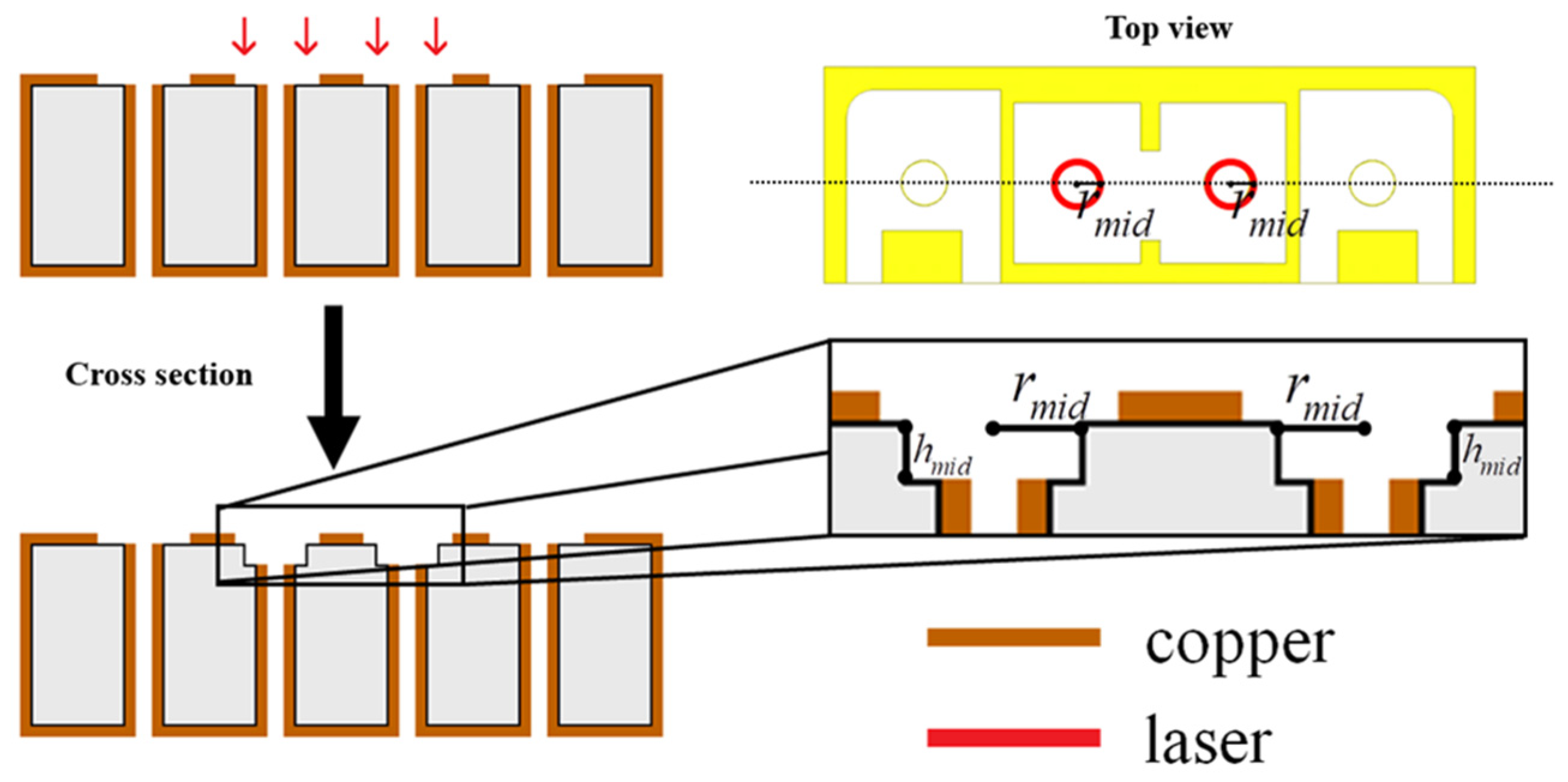
Figure 5 shows the top view and cross section of the laser trimming process. The cross section is based on the dashed line in the top-view diagram in Figure 5. The laser trimming process modifies the digging depth (hmid) and digging radius (rmid) of the two middle holes to adjust the frequency band and improve the in-band matching and loss. HFSS simulations were used to determine the trends with various hmid and rmid values, as well as to suggest the final hmid and rmid parameters for the real-world laser trimming performed later. The hole radius used in this project was 0.35 mm with an approximate error of ±25 µm. Therefore, the hole digging radius was initially set to a minimum of 0.4 mm and evaluated at different digging depths; a hole digging radius of 0.5 mm was similarly investigated.
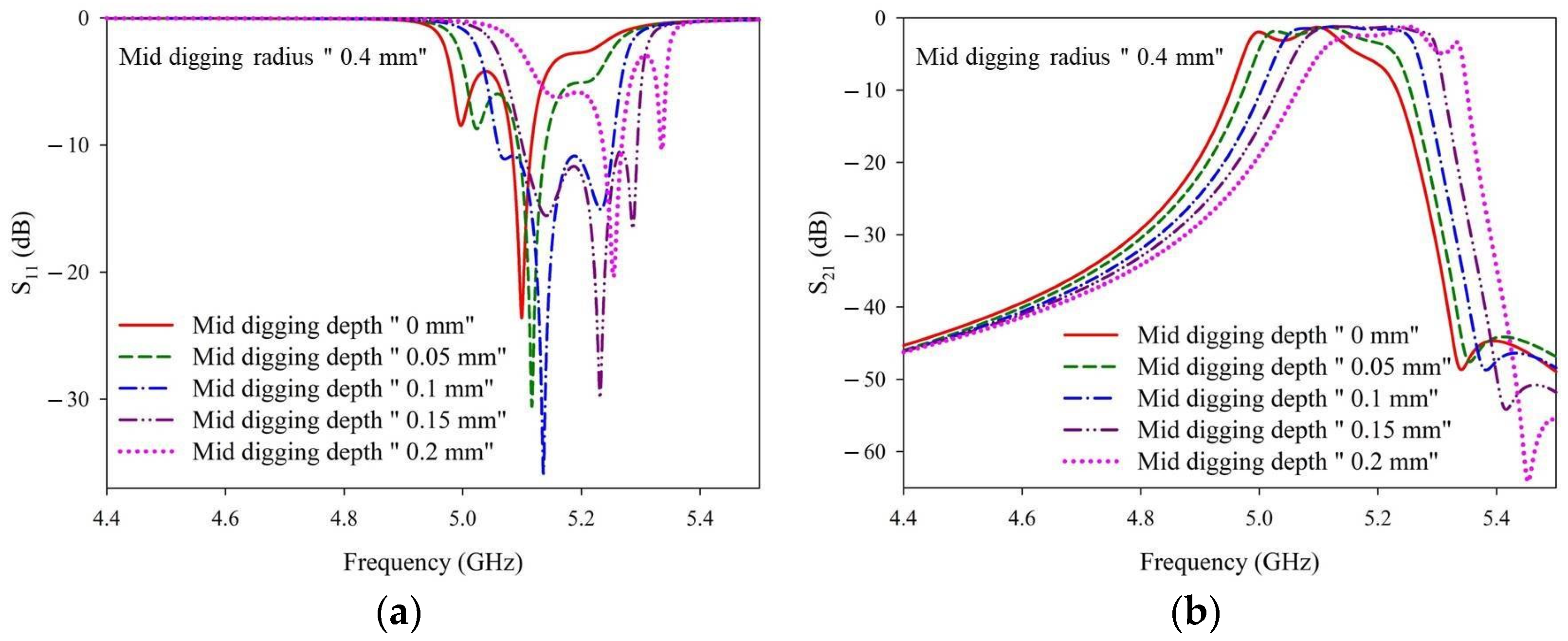
Figure 6 shows the S-parameters of these simulation results. The specific numbers of the corresponding curves are provided in Table A1. When the radius of the digging hole was fixed at 0.4 mm and the depth was increased from 0 mm to 0.15 mm in increments of 0.05 mm, the S11 value tended to be lower, and the frequency band shifted to a higher frequency. The optimal depth falls between 0.1 mm and 0.15 mm; however, as the depth was further increased to 0.2 mm, the frequency band continued to shift toward higher frequencies but the S11 values increased.
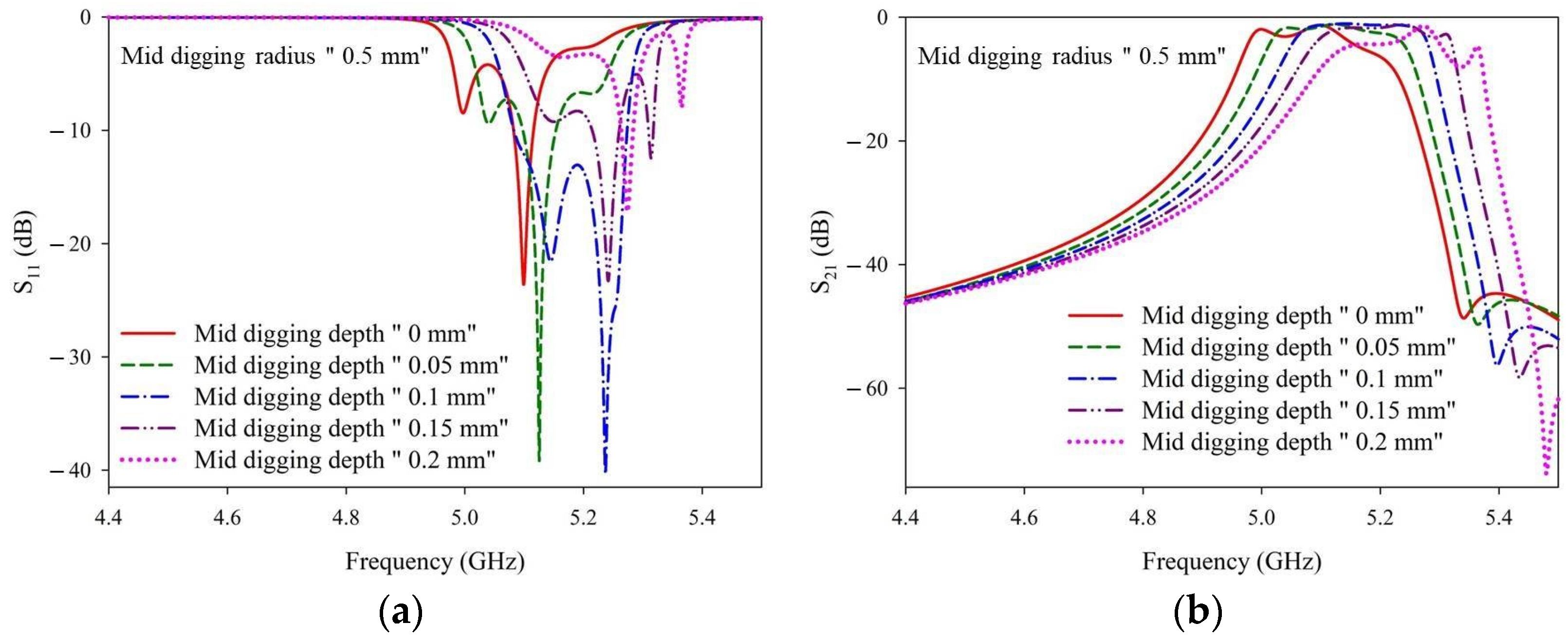
Figure 7 shows the S-parameter results with the digging radius fixed at 0.5 mm and various digging depths. The specific numbers of the corresponding curves are detailed in Table A2. The simulations run at digging radii of 0.4 and 0.5 mm showed similar trends, wherein the S11 value has the tendency to be lower, while the frequency band shifts to a higher frequency with a larger digging depth. When the fixed digging radius was 0.5 mm, the best performance was achieved with a digging depth of approximately 0.1 mm. The simulation results shown in Figure 6 and Figure 7 and Table A1 and Table A2 reveal that even with different digging radii, an appropriate digging depth can provide desired filter specifications. The digging depth in the subsequent simulations was set as 0.1–0.15 mm based on these obtained results.
Figure 8 shows the simulated S-parameters with a fixed digging depth of 0.1 mm and various digging radii. The specific values of the corresponding curves are given in Table A3. At a fixed digging depth of 0.1 mm, the input matching (S11) will be slightly lower and the rejection (S21 at ~5.4 GHz) is slightly better with wider digging radius.
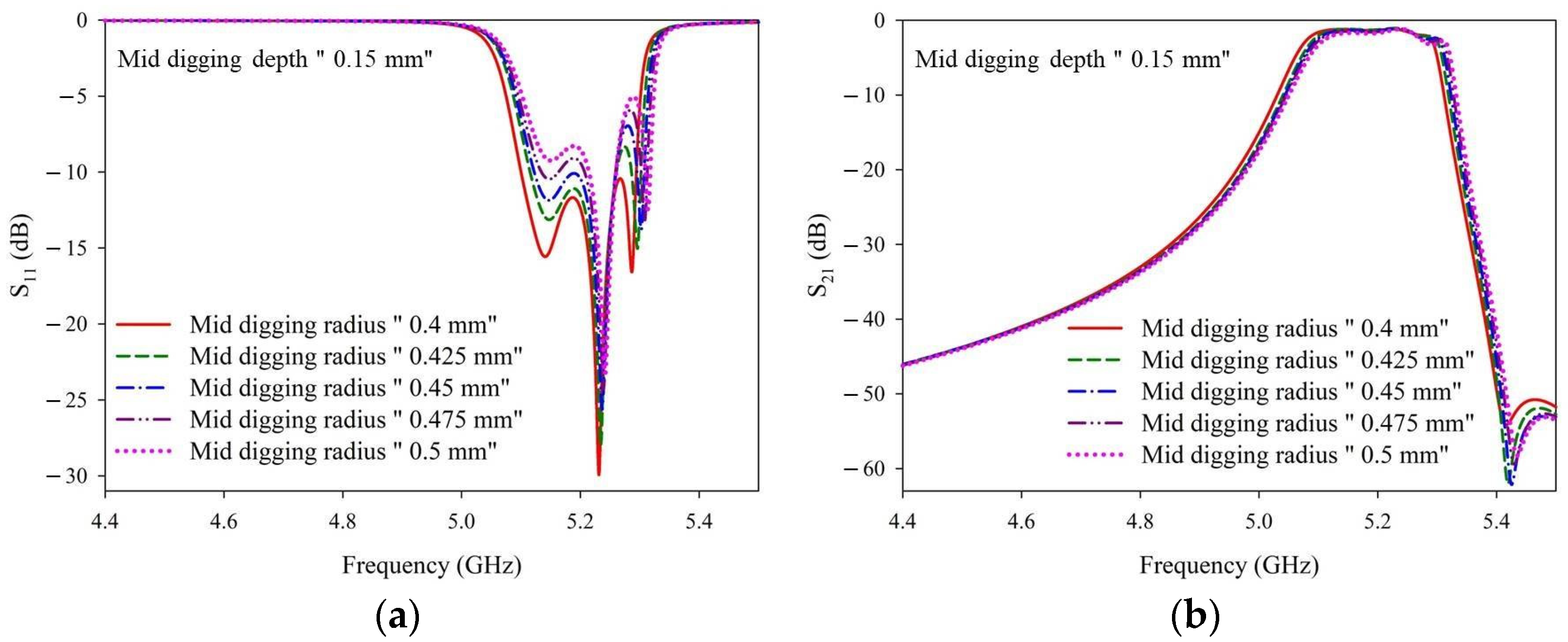
Figure 9 shows the simulated S-parameters obtained with a fixed digging depth of 0.15 mm and various digging radii. The detailed numbers of the corresponding curves are given in Table A4. With a fixed digging depth of 0.15 mm, the input matching (S11) was slightly higher/worse in the passband range. When considering the real-world laser trimming process, a YAG laser was applied. Owing to the heat accumulation around the operation areas, the more the YAG laser is utilized in the trimming process, the more difficult it is to control the digging depth and width after laser trimming. Therefore, a digging radius of 0.4 mm was used.

4. Laser Trimming Parameters, Operation Times, and Digging Depths

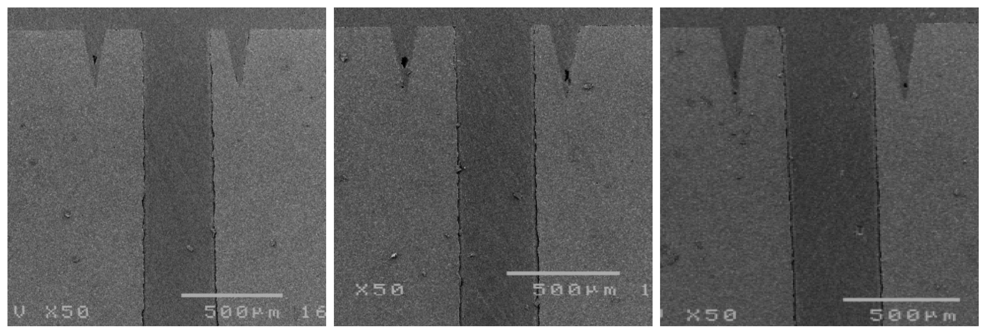
Simulations (Section 3) revealed that reducing the two middle holes shifts the frequency response to a higher frequency and smooths the frequency band. In this section, the laser trimming parameter recipe was investigated to meet the demands. Ceramic samples with and without metal surfaces were used for testing. After applying different laser trimming parameter recipes, the ceramic samples were cut and the digging depths were recorded. Four laser trimming parameters were evaluated: laser power (W), laser emitting frequency (kHz), processing speed (mm/s), and the number of repeated laser firings. These parameters were chosen because when a laser spot size is smaller than the designated trimming area radius, which is 350 µm in this study, the laser needs to repeatedly fire and move around the designated area to trim a uniform depth; this behavior can be investigated through the aforementioned parameters. Concerning notation, the parameter recipe of “5.5w_30k_300_re50” refers to a laser power of 5.5 W, a laser emitting frequency of 30 kHz, a processing speed of 300 mm/s, and 50 repetitions. In the early stage, the laser trimming zone was set as a donut type, as shown in Figure 10a. As mentioned in Section 3, the hole radius was 350 ± 25 µm. Consequently, a few smaller holes were not trimmed around the hole opening area, as shown in Figure 11. Figure 11 shows the cross-sectional images of the samples of three failed attempts using the donut-type laser trimming strategy. To avoid this type of failure, the laser trimming zone was changed to a circular type, as shown in Figure 10b.
Figure 12 shows the corresponding cross sections after different numbers of repeating laser firings with the 5.5w_30k_300_re50 recipe. Figure 12a–f show the cross sections of blank ceramic samples (i.e., those without metal surfaces) after one to six repetitions of laser firing, respectively; Table 3 summarizes the results shown in Figure 12. The results show that when the number of laser firings is more than three, the digging depths are approximately 325–361 µm because the laser goes out of focus while trimming deeper. For this process, the laser beam was set to focus on the ceramic top surface. As the number of repetitions increased, the hole edge became deeper. When the digging depth is greater than 300 µm, the laser goes out of focus and does not have enough power to dig deeper.
Table 4 summarizes the cross-sectional results of the ceramic samples with a metal thickness of 15 µm on the surface. From Table 4, it can be seen again that when the number of laser firings is greater than three, the depths are approximately 300 µm. Further, these results for samples with metal surfaces (Table 4) are consistent with those for samples without metal surfaces (Table 3).
As the electromagnetic simulations suggested in Section 3, the digging depth was approximately 0.1–0.15 mm; therefore, the 5.5w_30k_300_re50 trimming parameter recipe provided depths that were too great for this study. Therefore, after trying many combinations of laser trimming parameters, the laser trimming parameter recipes of 4w_30k_300_re10, 4w_30k_300_re20, and 4w_30k_100_re10 were selected for further investigations. The corresponding cross-section depths are summarized in Table 5, Table 6 and Table 7, respectively, as are those of the blank ceramic samples without metal surface.

5. Final Manufacture Process and Measurement Results

The final manufacturing process of the microwave dielectric ceramic filter is illustrated in Figure 13.
In Step 1, holes were drilled into the blank ceramic, while Steps 2 and 3 employed our previously reported [13] low-temperature process metallization process with laser patterning (Steps 1–3 are explained in detail in [13]). In Step 4, the ceramic surface around all four holes was partially trimmed. In Step 5, a lower trimming depth was utilized on the two middle holes to obtain the optimized results.
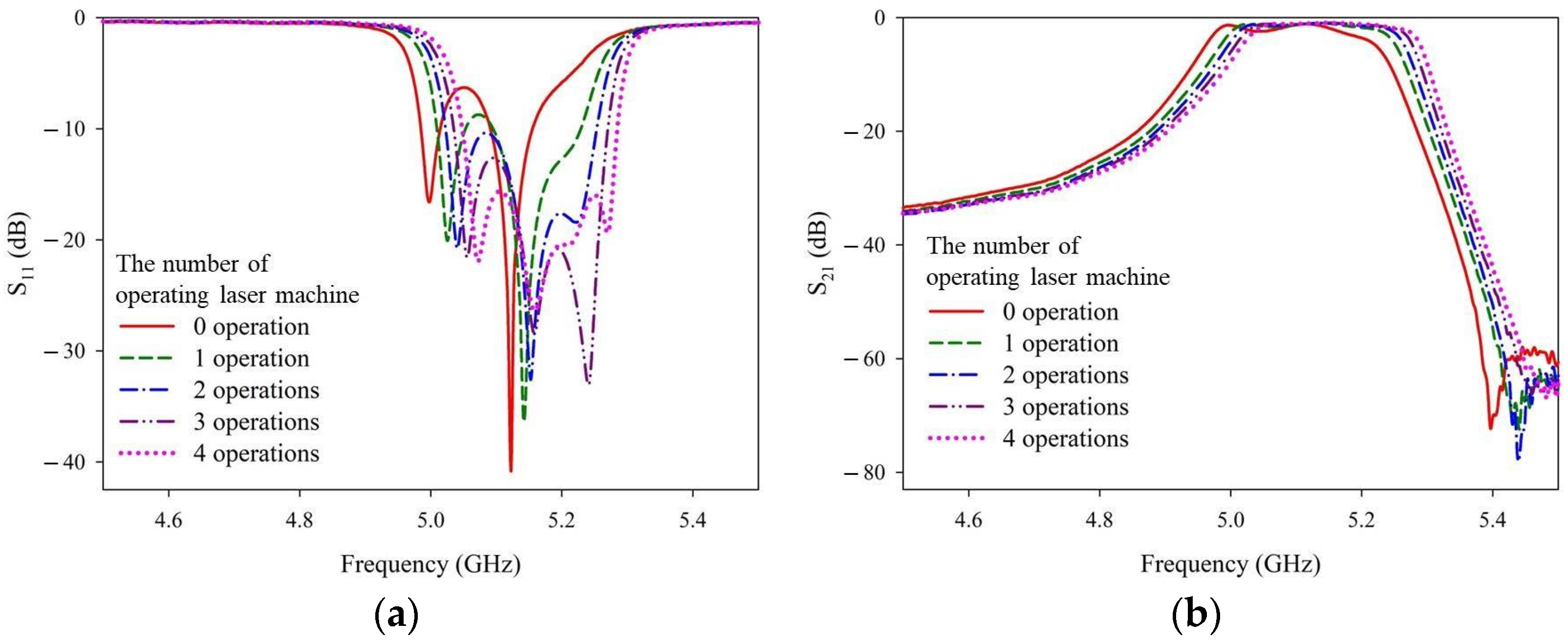
To obtain the approximate digging depth provided around the four holes in Step 4, the laser trimming parameter recipes of 4w_30k_300_re20 and 4w_30k_100_re10 were applied. After one operation (i.e., the number of repeated laser firings = 1), the ceramic filter sample was removed to measure and record the S-parameter characteristics. The ceramic filter sample was then returned and the process was repeated three more times (i.e., a total of four operations). Figure 14 and Figure 15 show the measurement results of the laser trimming parameter recipes 4w_30k_100_re10 and 4w_30k_300_re20, respectively.
The solid red curves represent ceramic filter samples without laser trimming. Figure 13 and Figure 14 show that the input matching (S11), in-band loss (S21), and band rejection (S21) shift toward higher frequencies with deeper digging depths (i.e., more operations) around the four holes. Upon comparing Figure 13 and Figure 14, several input matching (S11) curves in the passband lower end of recipe 4w_30k_100_re10 can be seen; these values are greater than −10 dB. However, these values are not as good as those of the 4w_30k_300_re20 recipe. Thus, recipe 4w_30k_300_re20 was selected for Step 4.
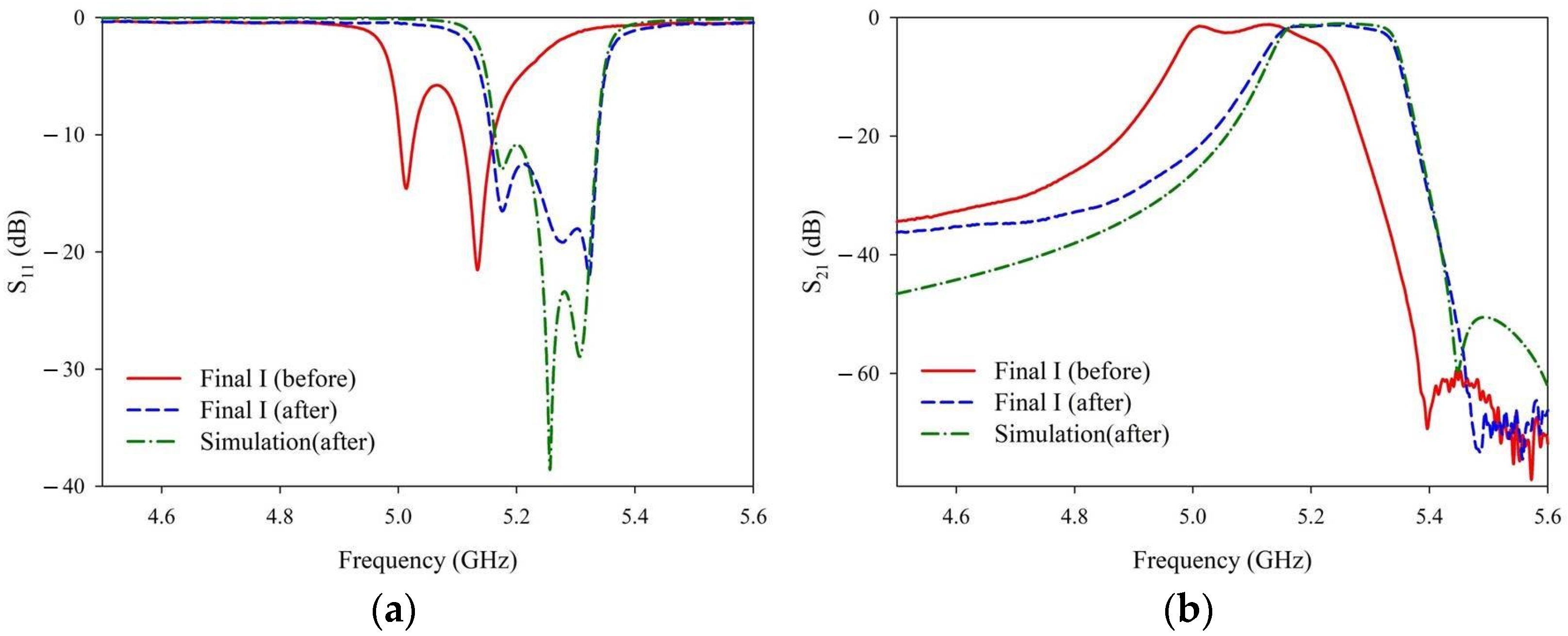
The final measurement results are presented in Figure 16 and Table 8. Figure 16 and Table 8 show the data before and after (measurements and simulation results) laser trimming. Step 4 of the final manufacturing process consists of two operation times using the 4w_30k_300_re20 recipe (Table 6), and Step 5 comprises another two operation times of the 4w_30k_300_re10 recipe (Table 5). As shown in Figure 16 and Table 8, the manufactured microwave dielectric ceramic filter meets design specifications after applying the proposed laser trimming recipes and manufacturing processes.
Figure 17 shows the photographs of the manufactured microwave dielectric ceramic filter. These photos clearly show that any metal around the hole openings was removed after laser trimming. At this stage, approximately ten microwave dielectric ceramic filters were manufactured in one round. The measurements were consistent among all ten, and met the target design criteria. This shows that the proposed recipes and processes are practical, effective, and can be applied to small-scale production. Comparisons between the conventional LTCC process and our proposed method are summarized in Table 9. The proposed process solves the metal clogging problem in the holes successfully. It also has less line width error and higher line position precision and can be applied to small-scale production.

6. Conclusions

In this study, microwave dielectric ceramics made of MgTiO3-CaTiO3 were metalized by electroless copper plating, and then patterned and optimized by a laser trimming process. Adopting this process can effectively save energy, production costs, and manufacturing time. The temperature employed for the entire microwave dielectric ceramic metallization process was below 50 °C. Thus, compared to other methods such as LTCC and DBC metallization, this technology can not only effectively reduce energy, but also greatly reduce the time and cost of heating and cooling. In addition, the proposed method solves the problem of clogging or incomplete adherence in the holes by applying a conventional silver paste sintering process. For laser engraving/trimming, the errors of the width and relative position of each line were within ±50 μm. Repeated laser trimming successfully adjusted the length of each resonant cavity to tune the device to the expected frequency band, and the digging depth was more accurately controlled than that observed for manual trimming. In addition to reducing the failure rate of product trimming, this strategy can also reduce labor costs and time. All measurements of the microwave dielectric ceramics fabricated using the proposed process met the desired design criteria. Moreover, approximately ten microwave dielectric ceramic filters can be manufactured in one round in the laboratory. The measurements among the ten filters were consistent, and met the criteria. This demonstrates that the proposed recipes and processes are practical and effective and can be applied to small-scale production.

Author Contributions

Conceptualization, J.-J.L., T.-H.K. and M.-C.H.; Methodology, J.-J.L., T.-H.K. and M.-C.H.; Software, J.-J.L. and C.-I.L.; Validation, J.-J.L., C.-I.L., T.-H.K. and M.-C.H.; Formal Analysis, J.-J.L., C.-I.L., T.-H.K. and M.-C.H.; Investigation, J.-J.L., C.-I.L., T.-H.K. and M.-C.H.; Resources, T.-H.K. and M.-C.H.; Data Curation, J.-J.L.; Writing—Original Draft Preparation, J.-J.L. and C.-I.L.; Writing—Review & Editing, J.-J.L.; Visualization, J.-J.L. and C.-I.L.; Supervision, J.-J.L. and M.-C.H.; Project Administration, J.-J.L. and M.-C.H.; Funding acquisition, J.-J.L. All authors have read and agreed to the published version of the manuscript.

Funding

This research was funded by the Ministry Of Science And Technology, Taiwan, grant number MOST 109-2221-E-018-007-.

Institutional Review Board Statement

Not applicable.

Informed Consent Statement

Not applicable.

Data Availability Statement

The data presented in this study are available on request from the corresponding author. The data are not publicly available due to their association with an ongoing study.

Acknowledgments

The manufacturing performed in this study was supported by Mechanical and Mechatronics Systems Research Laboratories, Industrial Technology Research Institute (ITRI), Taiwan.

Conflicts of Interest

The authors declare no conflict of interest. The funders had no role in the design of the study; the collection, analysis, or interpretation of data; the writing of the manuscript; or the decision to publish the results.

Appendix A

Table A1. The simulation results obtained with a fixed digging radius of 0.4 mm and various digging depths.
Digging Hole
Depth (mm)
fL
(GHz)
fH
(GHz)
BW
(MHz)
The Highest S11 Value in Passband (dB)S21 < −3 dB in Passband?
04.9845.132148−4.205.028–5.049 < −3 dB
0.055.0085.176168−5.97Yes (Bad S11)
0.15.0435.256213−10.84Yes
0.155.0765.293217−10.43Yes
0.25.1315.281150−5.85Yes (Bad S11)
Table A2. The simulation results obtained with a fixed digging radius of 0.5 mm and various digging depths.
Digging Hole
Depth (mm)
fL
(GHz)
fH
(GHz)
BW
(MHz)
The Highest S11 Value in Passband (dB)S21 < −3 dB in Passband?
04.9845.132148−4.205.028–5.049 < −3 dB
0.055.0225.220198−6.66Yes (Bad S11)
0.15.0615.274213−13.05Yes
0.155.1045.315211−5.055.280–5.303< −3 dB
0.25.2455.29247-----Fail
Table A3. The simulation results obtained with a fixed digging depth of 0.1 mm and various digging radii.
Digging Hole
Depth (mm)
fL
(GHz)
fH
(GHz)
BW
(MHz)
The Highest S11 Value in Passband (dB)S21 < −3 dB in Passband?
0.45.0435.256213−10.84Yes
0.4255.0455.260215−11.30Yes
0.455.0505.265215−11.94Yes
0.4755.0565.270214−12.50Yes
0.55.0615.274213−13.05Yes
Table A4. The simulation results obtained with a fixed digging depth of 0.15 mm and various digging radii.
Digging Hole
Depth (mm)
fL
(GHz)
fH
(GHz)
BW
(MHz)
The Highest S11 Value in Passband (dB)S21 < −3 dB in Passband?
0.45.0765.293217−10.43Yes
0.4255.0875.301214−8.33Yes (Bad S11)
0.455.0935.306213−6.95Yes (Bad S11)
0.4755.0975.311214−5.92Yes (Bad S11)
0.55.1045.315211−5.055.280–5.303 < −3 dB

References

  1. Liu, B.; Sha, K.; Zhou, M.F.; Song, K.X.; Huang, Y.H.; Hu, C.C. Novel low-εr MGa2O4 (M = Ca, Sr) microwave dielectric ceramics for 5 G antenna applications at the Sub-6 GHz band. J. Eur. Ceram. Soc. 2021, 41, 5170–5175. [Google Scholar] [CrossRef]
  2. Szwagierczak, D.; Synkiewicz-Musialska, B.; Kulawik, J.; Pałka, N. LTCC and Bulk Zn4B6O13–Zn2SiO4 Composites for Submillimeter Wave Applications. Materials 2021, 14, 1014. [Google Scholar] [CrossRef]
  3. Zhang, R.; Liu, J.; Wang, Y.; Luo, Z.; Zhang, B.; Duan, J. Flexible Wearable Composite Antennas for Global Wireless Communication Systems. Sensors 2021, 21, 6083. [Google Scholar] [CrossRef]
  4. Lee, B.D.; Yoon, K.H.; Kim, E.S.; Kim, T.H. Microwave dielectric properties of CaTiO3 and MgTiO3 thin films. Jpn. J. Appl. Phys. 2003, 42, 6158. [Google Scholar] [CrossRef]
  5. Huang, C.-L.; Weng, M.-H. Improved high Q value of MgTiO3-CaTiO3 microwave dielectric ceramics at low sintering temperature. Mater. Res. Bull. 2001, 36, 2741–2750. [Google Scholar] [CrossRef]
  6. Hao, S.; Shun-Hua, W.; Hai-yang, Y. Dielectric properties of B2O3 doped MgTiO3-CaTiO3 system ceramics. J. Wuhan Univ. Technol., Mater. Sci. Ed. 2004, 19, 62–64. [Google Scholar] [CrossRef]
  7. Jantunen, H.; Rautioaho, R.; Uusimäki, A.; Leppävuori, S. Compositions of MgTiO3–CaTiO3 ceramic with two borosilicate glasses for LTCC technology. J. Eur. Ceram. Soc. 2000, 20, 2331–2336. [Google Scholar] [CrossRef]
  8. Tummala, R.R. Ceramic and glass-ceramic packaging in the 1990s. J. Am. Ceram. Soc. 1991, 74, 895–908. [Google Scholar] [CrossRef]
  9. Sebastian, M.T.; Jantunen, H. Low loss dielectric materials for LTCC applications: A review. Int. Mater. Rev. 2008, 53, 57–90. [Google Scholar] [CrossRef]
  10. Narang, S.B.; Bahel, S. Low loss dielectric ceramics for microwave applications: A review. J. Ceram. Process. Res. 2010, 11, 316–321. [Google Scholar]
  11. Li, W.; Huang, M.; Kao, T.; Chung, W.; Chou, M. Novel LIM (Laser Induced Metallization) technologies of ITRI applied to WWAN/LTE 2-port antenna array for smart handset applications. In IEEE Antennas and Propagation Magazine, Proceedings of the 2014 International Symposium on Antennas and Propagation Conference Proceedings, Kaohsiung, Taiwan, 2–5 December 2014; Institute of Electrical and Electronics Engineers: Piscataway, NJ, USA, 2014; pp. 599–600. [Google Scholar]
  12. Yang, C.; Chou, M.; Kao, T.; Huang, M. Applications of Three Dimensional Laser Induced Metallization Technology with Polymer Coating. In Proceedings of the 2018 13th International Congress Molded Interconnect Devices (MID), Würzburg, Germany, 25–26 September 2018; pp. 1–6. [Google Scholar]
  13. Lin, J.-J.; Lin, C.-I.; Kao, T.-H.; Huang, M.-C. A Novel Low Temperature Process for Microwave Dielectric Ceramics Metallization. Appl. Comput. Electromagn. Soc. J. 2019, 34, 1601–1606. [Google Scholar]
  14. Rawat, B.S.; Beilke, L.; Miller, R.E. Design of a tapered coaxial resonator filter for mobile communications. IEEE Trans. Veh. Technol. 1992, 41, 1–5. [Google Scholar] [CrossRef]
  15. Maas, S. Coaxial Resonator Filters. Master’s Thesis, Stellenbosch University, Stellenbosch, South Africa, 2011. [Google Scholar]
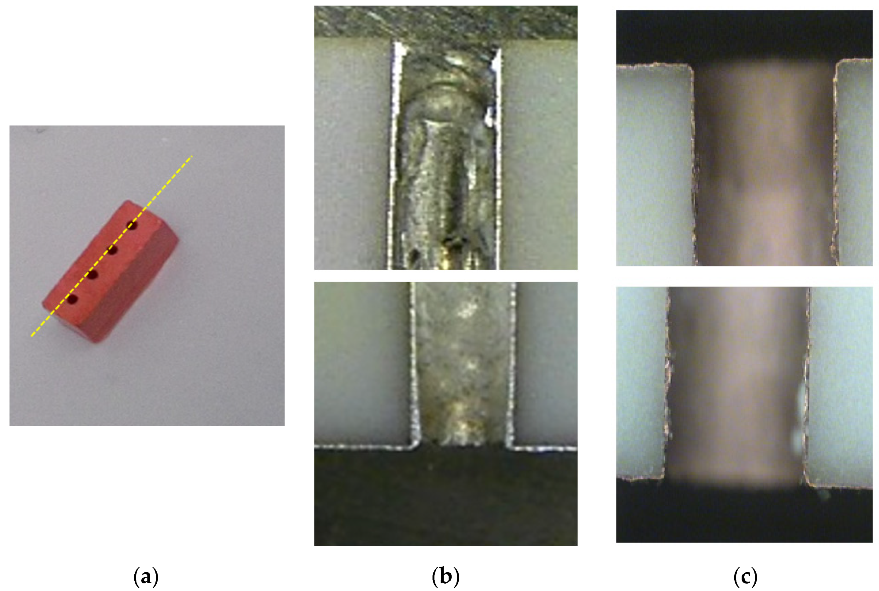
Figure 1. (a) A microwave dielectric ceramic filter; (b) Cross sections obtained with a conventional low-temperature co-fired ceramics (LTCC) process; (c) Cross sections obtained with the proposed low-temperature metallization process.
Materials 14 07519 g001
Figure 2. The microwave dielectric ceramic filter structure.
Materials 14 07519 g002
Figure 3. The complete low-temperature metallization and laser trimming processes.
Materials 14 07519 g003
Figure 4. The detailed steps of the low-temperature metallization process.
Materials 14 07519 g004
Figure 5. The top view and cross section of laser trimming processes.
Materials 14 07519 g005
Figure 6. (a) S11 and (b) S21 simulation results with a fixed digging radius of 0.4 mm and various digging depths.
Materials 14 07519 g006
Figure 7. (a) S11 and (b) S21 simulation results with a fixed digging radius of 0.5 mm and various digging depths.
Materials 14 07519 g007
Figure 8. (a) S11 and (b) S21 simulation results with a fixed digging depth of 0.1 mm and various digging radii.
Materials 14 07519 g008
Figure 9. (a) S11 and (b) S21 simulation results with a fixed digging depth of 0.15 mm and various digging radii.
Materials 14 07519 g009
Figure 10. Two laser trimming strategies: (a) donut type and (b) circular type.
Materials 14 07519 g010
Figure 11. Cross sections of three samples unsuccessfully trimmed with a donut-type laser trimming strategy.
Materials 14 07519 g011
Figure 12. The cross sections of samples trimmed for different numbers of repeated laser firings with the 5.5w_30k_300_re50 recipe (no metal surface): (a) one; (b) two; (c) three; (d) four; (e) five; and (f) six repetitions.
Materials 14 07519 g012
Figure 13. The final manufacturing process of the microwave dielectric ceramic filter.
Materials 14 07519 g013
Figure 14. Measured (a) S11 and (b) S21 values after different numbers of operations with the 4w_30k_100_re10 recipe.
Materials 14 07519 g014
Figure 15. Measured (a) S11 and (b) S21 values after different numbers of operations with the 4w_30k_300_re20 recipe.
Materials 14 07519 g015
Figure 16. Measured (a) S11 (b) S21 values of the filter before laser trimming and after laser trimming (measurements and simulation results).
Materials 14 07519 g016
Figure 17. The manufactured microwave dielectric ceramic filter: (a) The laser trimming the opening parts of the through-holes; (b) Closer view of the two middle holes.
Materials 14 07519 g017
Table 1. The properties of selected MgTiO3-CaTiO3 materials.
MaterialDk Q × f (GHz)Sintering Temperature (°C)TCK (ppm/°C)
MgTiO3 [4]1716,000 @ 7 GHz800−50
CaTiO3 [4]1703600 @ 7 GHz800800
0.95 MgTiO3-0.05 CaTiO3 + 2 wt%B2O3 [5]21.262,000 @ 8 GHz14004
0.95 MgTiO3-0.05 CaTiO3 + 3.5 wt%B2O3 [6]20.368,000 @ 6 GHz1210−5
MgTiO3-CaTiO3 [7]18–204000 @ 6 GHz1360−10 to 10
Abbreviations. Dk = dielectric constant, Q × f = quality factor at the corresponding frequency, TCK = temperature coefficient of dielectric constant.
Table 2. The microwave dielectric ceramic filter specifications.
PassbandInput and Output Matching (S11 and S22)In-Band Loss (S21 and S12)Image Rejection at ~5.5 GHz
fL
(GHz)
fH
(GHz)
BW
(MHz)
5.155.33180<−10 dB>−3 dB<−60 dB
Table 3. The measured depth values after different numbers of repeated laser firings with the 5.5w_30k_300_re50 (no metal surface) recipe.
Number of Repeated Laser FiringsDepth on the Left Edge (µm)Depth on the Right Edge (µm)Depth Difference (µm)Depth Average (µm)
One1331249143.5
Two24122219231.5
Three2892967292.5
Four34833711342.5
Five31633115338.5
Six32033010325
Table 4. The measured depth values after different numbers of repeated laser firings with the 5.5w_30k_300_re50 (15-µm metal surface) recipe.
Number of Repeated Laser FiringsDepth on the Left Edge (µm)Depth on the Right Edge (µm)Depth Difference (µm)Depth Average (µm)
One1701744172
Two2872969291.5
Three27631539295.5
Four30233634319
Five29134352317
Six30033030315
Table 5. The measured depth values after different numbers of repeated laser firings with the 4w_30k_300_re10 recipe.
Number of Repeated Laser FiringsDepth on the Left Edge (µm)Depth on the Right Edge (µm)Depth Difference (µm)Depth Average (µm)
One15.9022.977.0719.44
Two37.1045.948.8441.52
Three70.6777.767.0974.22
Four72.4670.671.7971.57
Table 6. The measured depth values after different numbers of repeated laser firings with the 4w_30k_300_re20 recipe.
Number of Repeated Laser FiringsDepth on the Left Edge (µm)Depth on the Right Edge (µm)Depth Difference (µm)Depth Average (µm)
One24.7330.095.3627.41
Two65.3793.6428.2779.51
Three132.51123.698.82128.10
Four153.71166.0812.37159.90
Table 7. The measured depth values after different numbers of repeated laser firings with the 4w_30k_100_re10 recipe.
Number of Repeated Laser FiringsDepth on the Left Edge (µm)Depth on the Right Edge (µm)Depth Difference (µm)Depth Average (µm)
One65.3961.843.5563.62
Two98.96104.255.29101.61
Three120.14134.2814.14127.21
Four162.54178.4515.91170.50
Table 8. Summary of parameters before laser trimming and after laser trimming (measurements and simulation results).
fL
(GHz)
fH
(GHz)
BW
(MHz)
Highest S11 Value in Passband (dB)S21 > −3 dB in Passband?Image Rejection < −60 dB at ~5.5 GHz
Measured data (before)4.9915.178187−5.76Yes (Bad S11)Yes
Measured data (after)5.155.33180−11.77YesYes
Table 9. Comparisons between the conventional LTCC process and the proposed process.
LTCC Process [7]Proposed Process
Temperature of metallization process (°C)900~1000<50
Metal clogged in holesYesNo
Minimum metal line width (µm)10050
Relative position of lines (µm)±100±50
Mass productionYesNot yet
Publisher’s Note: MDPI stays neutral with regard to jurisdictional claims in published maps and institutional affiliations.