3.1. The Characterization of Surface Morphology
The observation of samples’ surfaces from SEM images provides microscopic details of porous coatings with which the characteristics of surface morphology can be analyzed.
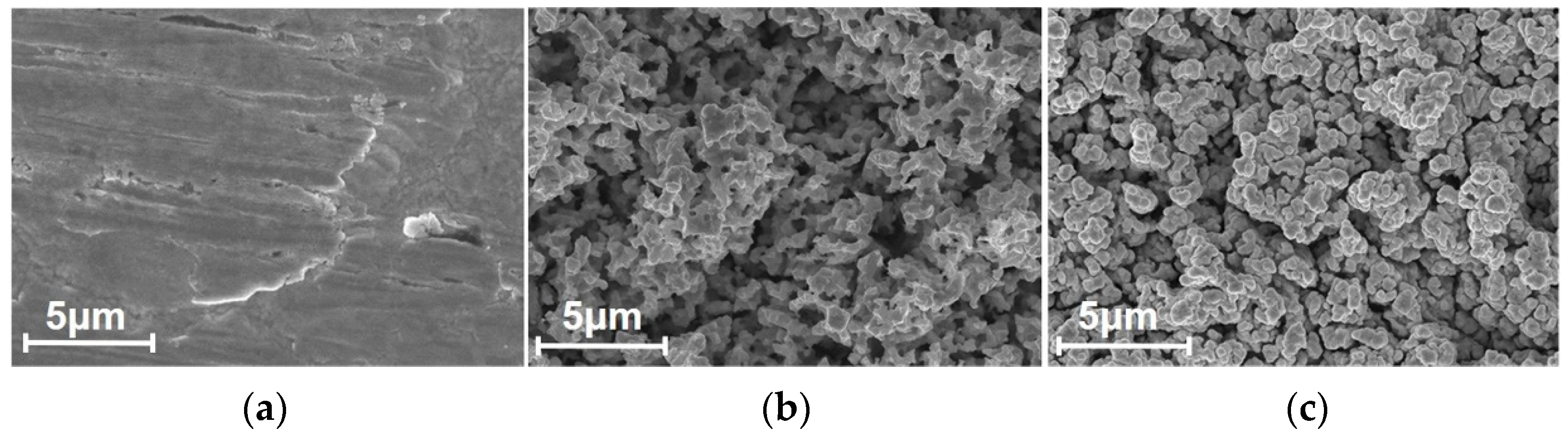
Figure 2 presents the evolution of samples’ surface morphologies in the process using the parameter scheme
D4. The surface of the sample with nickel and silver layers in
Figure 2a appeared to be plate-like and smooth before wet etching. In
Figure 2b, the microstructures produced via etching made the surface rugged and porous. After gold sputtering, the edges and corners of the porous microstructures become gentle and rounded into sphere-like, granular clusters, as shown in
Figure 2c. However, this characteristic of granular morphology was not universal in all of the schemes.
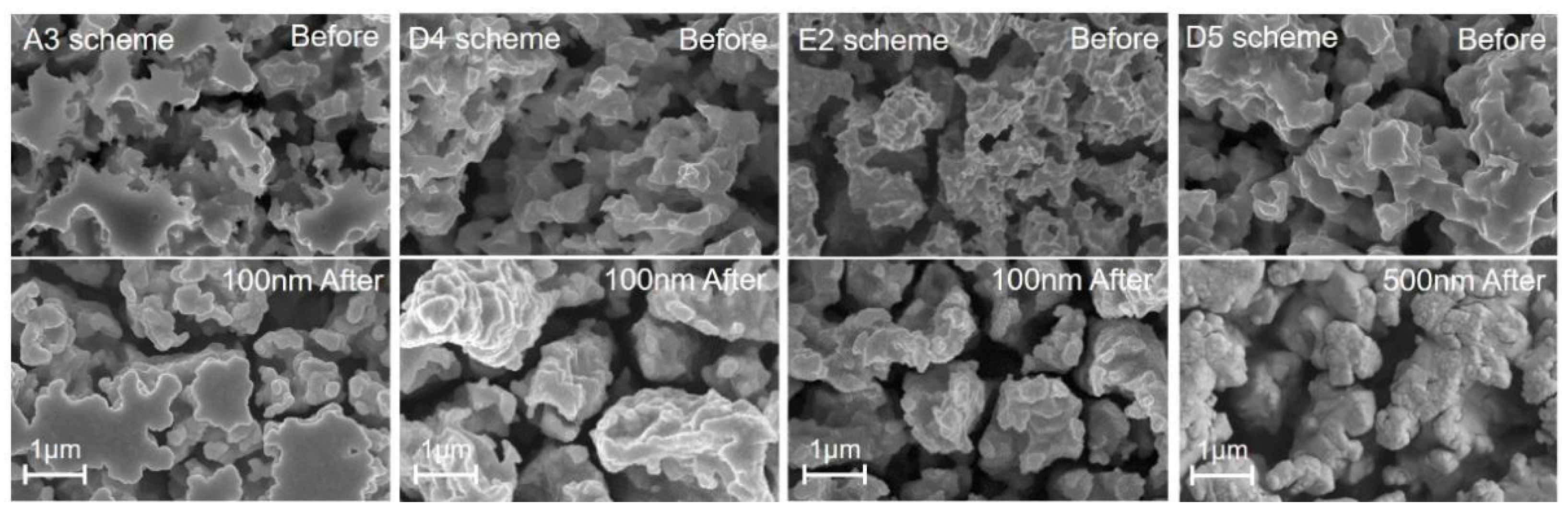
Figure 3 shows the porous microstructures before and after gold coating was obtained using different schemes, and these schemes led to a tremendous difference in surface morphology. The microstructure produced using the
A3 scheme before gold coating had islands and a flat top, while the structures produced using the
D4 scheme appeared to have porous granular morphologies with uniformity. The resulting porous structures from different schemes were different in terms of porosity and particle size, which was reflected in the difference in morphology before gold coating between the
E2 scheme and the
D5 scheme. After gold coating, wrapping and filling with the gold layer made the characteristics of surface morphology more obvious. However, the application of a 500 nm gold layer on the porous structures of the
D5 scheme made it become granular, and fine structures disappeared. With a further increase in the thickness of the gold layer, the discrepancy in the surface morphology due to this thickness could potentially affect the surface SEY that corresponded to different schemes.
In order to quantitatively describe the difference between these morphological features, a parameter
, called the characteristic pore size of a porous structure, was defined as the average distance between adjacent visible particles in a sampling area on porous surface structures. It could be calculated using Equation (1) according to SEM images, where
n is the number of pores and
represents the size of each individual pore which is usually on the micron scale.
i circulates from 1 to
n to calculate the average size of n pores in an image, and the result is accurate to one decimal place. Thus, the
values for the SEY images corresponding to different schemes could be calculated, as shown in
Table 2.
While
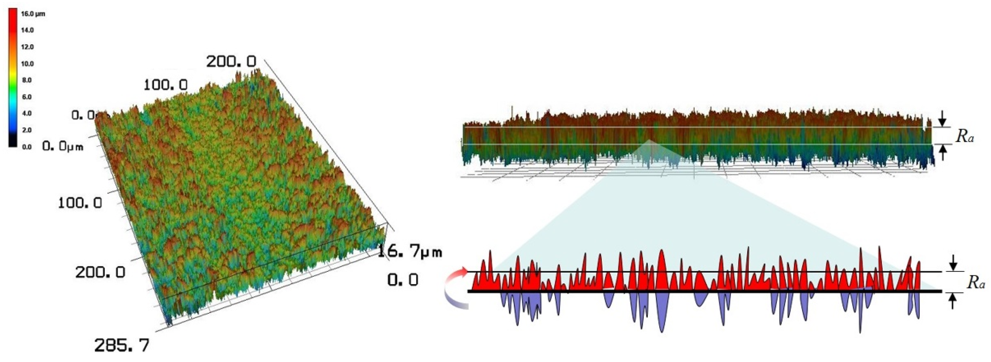
reflects the real appearance of porous structures, it cannot be obtained using large-scale measurements. Therefore, the values of the absolute average relative to the base height of 3D surface profiles,
, were used to characterize surface roughness. The value of
was obtained by extracting surface height information measured using a color laser scanning microscope (LSM), and it was calculated according to Formula (2).
provided the average difference between peaks and valleys. It was more appropriate for use in the macroscopic evaluation of surface morphology, while
was advantageous to use in the analysis of local microporous structures. An example of gaining
from a surface profile is shown in
Figure 4, which outlines the process of extracting and processing profile information. This underpins the average
values of some representative schemes presented in
Table 2. It should be noted that
reflected the arithmetic average of the absolute values of the deviation from the points on the actual profile to its profile centerline within a selected area. Additionally, the
values for schemes in
Table 2 were averages of the
measurements of several substrates with this scheme. The
measurement of one substrate was also an average of five sampling areas on a same substrate, which eliminated the effect of a random defect in one sampling area.
3.2. The Measurements of Secondary Electron Yield
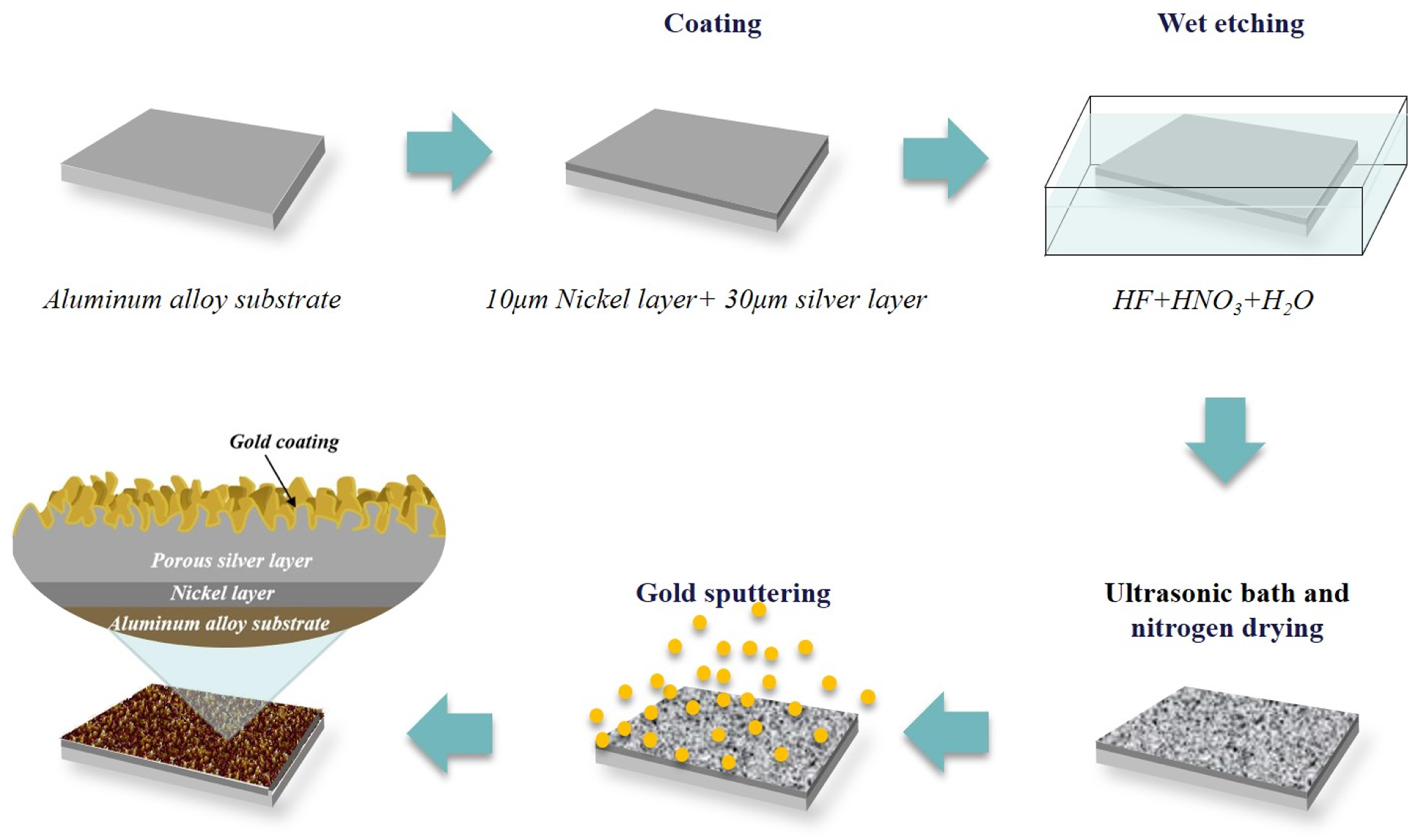
The SEY measurement system is outlined in
Figure 5. The electron beam irradiated the target sample surface with primary energy from 30 eV to 3000 eV, which could be adjusted by the output of a DC power. The emitted SEs were entirely collected by the collector biased with a positive potential of 40 V. The secondary electrons current
and the target current
could be measured using the continuously irradiated method, and then the primary electron current
was obtained as
. The SEY value
δ could finally be calculated using:
Figure 6 presents the SEY results of substrates before and after the surface treatment with some different process schemes. Notably, the SEY result for each scheme is an average of the SEY measurements of five samples, and the measured value of each sample is also an average of the results of several sampling areas selected on it. It was found that the
, the average value of the maximum SEY as a function of the primary electron energy, decreased a lot after the treatment. The
for substrates decreased from 2.2 (with the error of 0.4) to 1.1 (within ±0.03) ~1.2 with the
D4 scheme for the 100 nm gold batch (
D4-100n) and the
D4 scheme for the 500 nm gold one (
D4-500n), in which the best SEY suppression reached 54% in the
D4-100n scheme. For more evidence to indicate the great differences in the final
values caused by process schemes, the
results corresponding to ten schemes with 100 nm-thick gold coatings are shown in
Table 3. More results of
for schemes in
Table 1 are shown in
Appendix A Table A1 and
Table A2.


 ,
, 