Abstract
Two-dimensional van der Waals crystals (2D vdW) are recognized as one of the potential materials to solve the physical limits caused by size scaling. Here, vdW metal oxide MoO3 is applied with the gate dielectric in a 2D field-effect transistor (FET). Due to its high dielectric constant and the good response of MoS2 to visible light, we obtained a field effect transistor for photodetection. In general, the device exhibits a threshold voltage near 0 V, Ion/Ioff ratio of 105, electron mobility about 85 cm2 V−1 s−1 and a good response to visible light, the responsivity is near 5 A/W at low laser power, which shows that MoO3 is a potential material as gate dielectric.
Keywords:
MoS2; MoO3; FET; photodetector; field effect transistor; gate dielectric; transistor; van der Waals materials 1. Introduction
There is no doubt that the transistor is an indispensable part of modern life, it is the brain of all electronic devices today. Unfortunately, the short channel effect caused by the reduction in channel size and the direct electron tunneling caused by the decrease in dielectric layer thickness seriously restricts the performance of devices [1,2,3,4]. Two-dimensional van der Waals materials (2D vdW) with superior carrier migration and excellent gate controllability at atomic thickness are considered as the next-generation potential channel materials [5]. In addition, since the capacitance is inversely proportional to the gate dielectric material thickness and proportional to the dielectric constant [6]. It can be seen that materials with high dielectric constant can satisfy the thickness reduction while providing strong capacitive coupling. To date, the 2D field-effect transistors supported by high-κ material substrate has been reported. For example, Ganapathi et al. fabricated MoS2 short channel devices with 5 nm-thick HfO2, achieving an extremely low threshold voltage (approximately −1 V), 106 switching ratio, and extremely low subthreshold swing (110~120 mV/dec) [7]. Ah-Jin Cho et al. also successfully fabricated the field effect devices using Al2O3 as the gate dielectric layer [8]. However, there are a lot of dangling bonds and surface trap states in the thin film dielectric layer, resulting in a large hysteresis. High-quality vdW dielectric has received much attention due to its atomic plane, hanging bonds-free, and low trap density. Hexagonal boron nitride (hBN) is the most common two-dimensional insulator and is widely regarded as a promising gate insulator in two-dimensional material transistors. However, the dielectric constant of hBN is only 5 [9]. Recently, Liu et al. showed that MoS2 field-effect transistors supported by Sb2O3 dielectric substrate exhibit negligible hysteresis [10]. However, the dielectric constant of Sb2O3 is also only 11.5, there is still a lot of room for improvement.
As a member of transition metal oxides (TMO), α-MoO3 is widely used in electronics, sensors, energy storage and other fields [11]. More importantly, α-MoO3 has high dielectric constant. It has been shown that α-MoO3 has the relative dielectric constant as high as 35, near 10 times that of SiO2 [12]. In addition, the unique vdW characteristics can be easily integrated with other 2D vdW semiconductors, promising applications in future 2D electronics and optoelectronics [13,14].
Here, we constructed the α-MoO3 flake support MoS2 field effect transistor. Thanks to high capacitive coupling, we achieve a low-threshold voltage (−1 V), which is lower than hBN (−2 V) and Sb2O3 (−7 V), and has greater electron mobility (85 cm2 V−1 s−1) compared to the SiO2 dielectric layer (41 cm2 V−1 s−1). In addition, due to the good response of MoS2 to visible light, combined with the excellent performance of the MoO3 gate dielectric layer, we can obtain photodetectors with higher responsivity (5 A/W).
2. Results and Discussion
2.1. Structural Characteristics of α-MoO3 Flakes
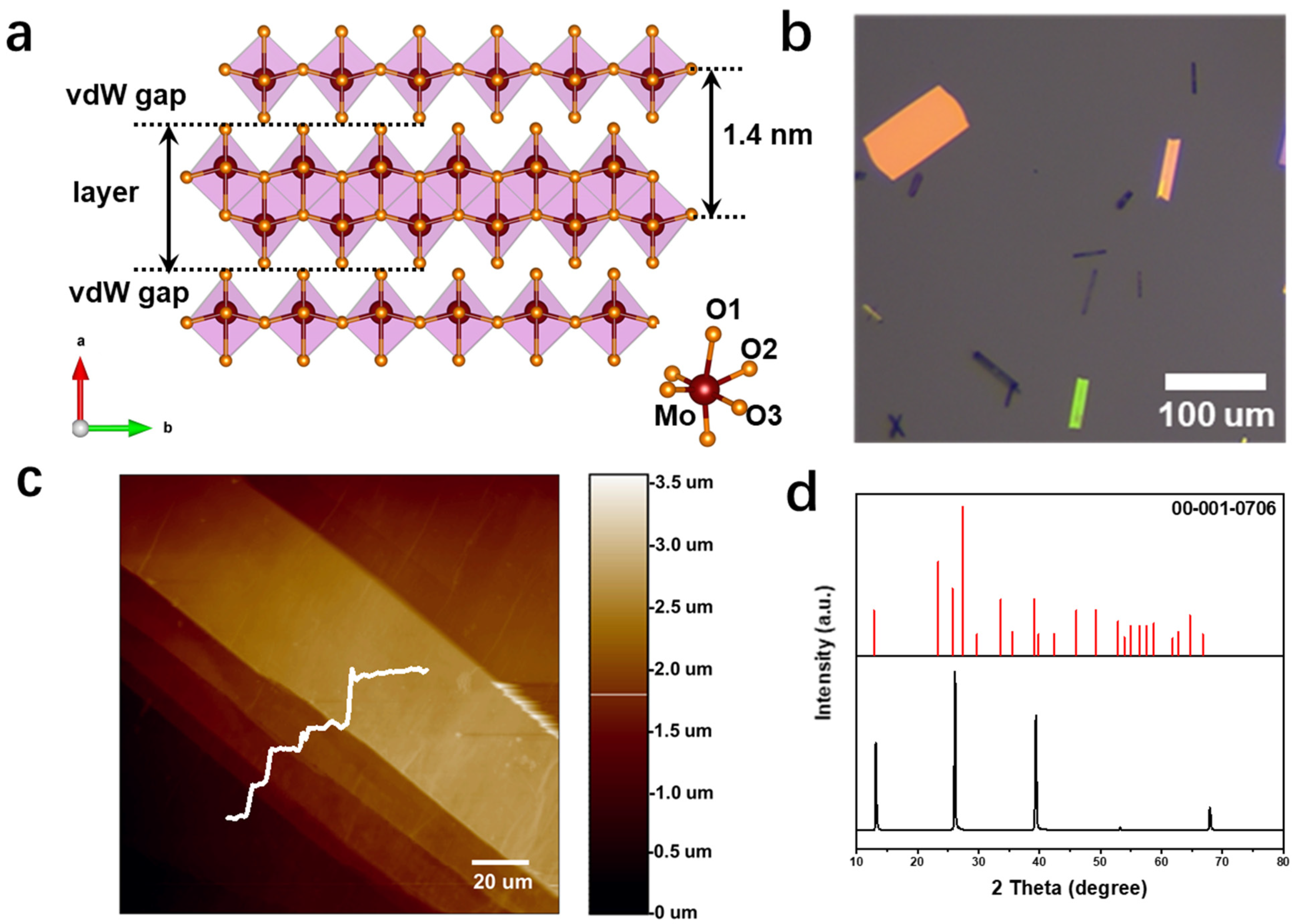
α-MoO3 is a wide-bandgap material (3 ev), has a large work function (6 ev), and is an orthorhombic crystal structure [15,16,17]. As shown in Figure 1a, it consists of double layers of MoO6 octahedrons of approximately 1.4 nm thickness. In each layer, the octahedrons are arranged by sharing angles in the directions [001] and [100], and the different layers are arranged in the direction [010] by van der Waals forces. The preparation of uniform large-size MoO3 nanosheets is the key to the application of the gate dielectric, so several α-MoO3 nanosheets were grown using rapid-cooling chemical vapor deposition (CVD) (growth details are shown in the experimental section and Figure S1) [18]. Figure 1b shows the optical image of the prepared MoO3 nanosheet. It can be seen that MoO3 nanosheet has a large area, with micron level length and width, regular shape and smooth surface. As show in Figure 1c, the layered structure of MoO3 is well illustrated by the multi-thickness steps at the edge in atomic force microscopy (AFM) image. XRD characterization revealed that the lattice has a series of sharp peaks at 13.7°, 26.6° and 39.8°, which correspond to the (020), (040), and (060) planes of α-MoO3, indicating the high quality of MoO3 single crystal (Figure 1d).

Figure 1.
(a) MoO3 lattice structure diagram. (b) Optical microscope image of MoO3 nanosheets grown by vapor deposition method. (c) AFM surface topography of MoO3 nanosheets. (d) XRD spectrum of MoO3 nanosheets.
2.2. Device Performance
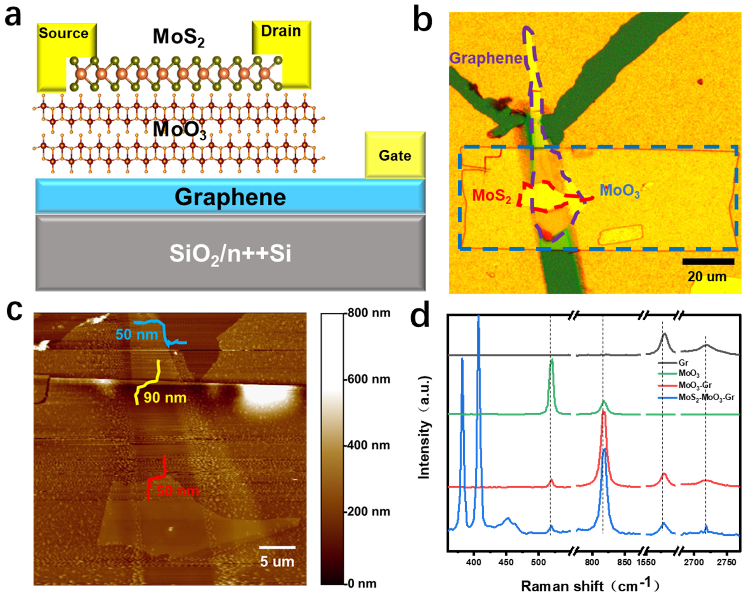
Good insulation is the key to gate dielectric applications, therefore, we first studied the insulation of MoO3 before preparing heterojunction devices. As shown in Figure S2, when the source–drain voltage (Vds) is 2 V, the MoO3 FET device presents a high resistance state of 10−13 A and remains stable under the action of gate voltage, suggesting the good insulation of MoO3. Furthermore, we constructed a graphene/MoO3/MoS2 field effect devices by the dry method of location transfer where graphene, MoO3 and MoS2 are the gate electrode, gate dielectric layer and channel layer, respectively (details are shown in the experimental section and Figure S3). An optical image of the prefabricated device is shown in Figure 2b. The AFM in Figure 2c shows that the corresponding thickness of MoS2, MoO3 and Gr are 50 nm, 90 nm and 50 nm, respectively. Raman spectroscopy is further used to confirm heterojunction composition. In the Raman spectrum of graphene, the G peak near 1580 cm−1 can correspond to the c–c σ bond of carbon atoms, reflecting the in-plane vibration of carbon atoms, while the G’ peak near 2700 cm−1 corresponds to carbon atom π-bond in the z direction, reflecting graphene-layered connections [19,20]. In the Raman spectrum of MoS2, the peak located near 386 cm−1 is caused by the opposite vibrations of the two S atoms relative to the Mo atom, while the A1g peak located near 408 cm−1 is due to the S atoms in opposite directions out-of-plane vibration [21]. In the Raman spectrum of MoO3, there is a strong Raman peak at 820 cm−1, which corresponds to the O3-Mo-O3 stretching vibration in the [100] direction [22]. Due to the special structure of MoO3, there may be oxygen vacancies inside, which will affect the electron mobility, band gap, etc. [23]. Thus, we calculated the exact MoO3 stoichiometry by analyzing the Raman spectrum. From the Raman spectrum of MoO3 in Figure 2d, the ratio of I512/I820 is approximately 3.997, and finally, we calculated the ratio of O/Mo to be approximately 2.998, which indicates that there are very few oxygen vacancies in the MoO3 nanosheets we used. In the Gr/MoO3/MoS2 heterojunction region, Raman signals corresponding to different materials can be obtained simultaneously, which proves the composition of the heterojunction.
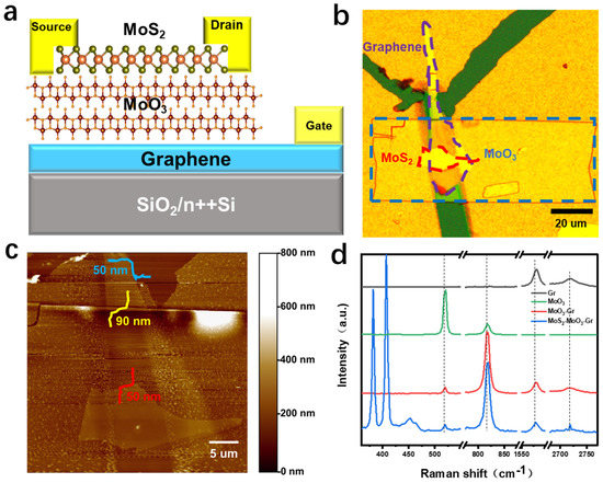
Figure 2.
(a) Schematic diagram of Gr/MoO3/MoS2 heterostructure. (b) Optical image of the device under optical microscope. (c) AFM surface topography of the device. (d) Raman spectra at different positions of the device.
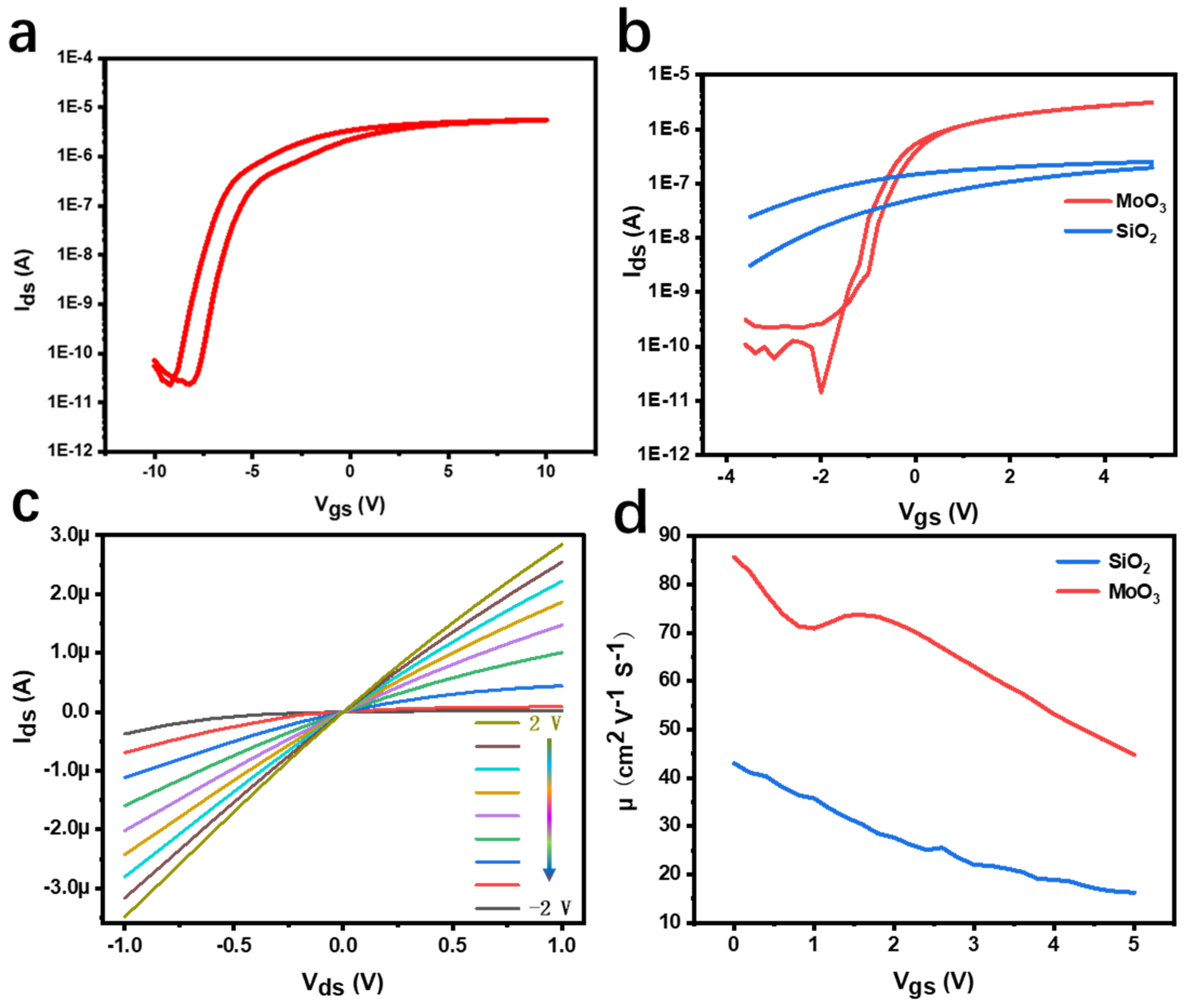
MoS2 FETs using MoO3 nanosheets as the gate dielectric show interesting device performance. Figure 3b shows the transfer curves of MoS2 FETs with different gate dielectric layers. Compared with SiO2 as the gate dielectric layer, it can be found that when the MoO3 nanosheet is used as the gate dielectric layer, MoS2 channel conductance increases with the increase in gate voltage, and obvious on–off current can be observed, showing obvious n-type modulation characteristics, which is caused by the natural sulfur vacancy of MoS2 [24]. Additionally, due to the low gate current leakage of ~10−11 A, this FET exhibits an equally high on/off ratio (~105). However, the MoS2 transistor using SiO2 as the gate dielectric layer cannot achieve obvious on–off state current within the same gate voltage range. By further increasing the gate voltage, we still observe that MoS2 channel conductance increases with increasing Vgs, because a larger Vgs may gradually open the whole channel and increase the conductivity of the whole channel. At the same time, it requires a more negative Vgs to close the channel, and a threshold voltage of approximately −9 V can be observed (Figure 3a). This indicates that MoS2/MoO3 FET has lower starting voltage and lower power consumption. In addition, the hysteresis of a transfer curve is usually used to study the charge trap state at the interface. The change of threshold voltage in the double-scan transmission characteristic curve is usually affected by the charge of the trap state density. It can be found that, with vdW dielectric, ultra-small hysteresis can be observed in the double scan, and the MoS2/SiO2 FET hysteresis window is quite big. According to
where and represent the gate capacitance and capture charge, respectively, the trap state density can be obtained as 9.8 × 1010 cm−2, while the trap state density of SiO2 is 1.4 × 1012 cm−2, indicating that MoO3 is within low effective trap state density. By processing transfer curve data (Figure 3b), we obtained that the subthreshold swing (SS) of molybdenum disulfide with MoO3 as the gate dielectric layer is basically stable at approximately 400 mV/dec. The gate control characteristics of the channel conductance and the ohmic contact between the electrode and MoS2 can be further verified from the output curve in Figure 3c. In order to clearly compare the effect of dielectric effects (MoO3 and SiO2) on FET mobility, we plot together their electron mobility, which is modulated by the gate voltage (Figure 3d). The electron mobility can be calculated by the following formula:
where and are the channel length and width, respectively, is the capacitance, and can be calculated as 3.27 × 10⁻⁷ F/cm2 by the following formula:
where , and are vacuum permittivity, relative permittivity and dielectric thickness of dielectric layers, respectively.

Figure 3.
(a) Transfer curves of the gate of SiO2 under more gate voltage range. (b) Comparison of transfer curves of different substrates under the same gate voltage range. (c) Output curves of the device, the interval is 0.5 V. (d) The relationship between the mobility of different substrates and gate voltage curve.
It was evident that MoS2 on MoO3 substrate showed approximately twice the mobility (85 cm2 V−1 S−1) compared with that on the SiO2 substrate (41 cm2 V−1 S−1).
Finally, we statistically compared the performance of this device with other MoS2 devices with difference gate dielectric layers (Table 1), showing that the MoO3 dielectric layer can still have a larger current switching ratio under the small threshold voltage, and its requirements on material thickness is also low.

Table 1.
Device data for different gate dielectric layers.
2.3. Device Mechanism Exploration
In order to further understand the carrier transport characteristics of heterojunction devices, Kelvin probe force microscopy (KPFM) was used to obtain the function of the surface potential position along the channel of the sample. Figure 4a is a schematic diagram of KPFM experiments on heterogeneous junction devices under different working conditions. We fixed the source–drain voltage Vds = 0 V and studied the functional relationship between the surface potential and back-gate voltage (Vgs). As shown in Figure 4b, since both ends of the source and drain are grounded, the corresponding surface potential is 0 V, while the channel has an obvious potential difference. When the gate voltage is between −10 V and −2 V, there is no obvious change in the surface potential difference. When the gate voltage rises to within the range of −2 V–0 V, the surface potential of the channel gradually rises, and then it exceeds the source–drain surface potential, and the potential difference is 0.5 V; the gate voltage continues to rise, the surface potential continues to rise, but the upward trend has weakened. Through the change of surface potential difference and the corresponding transfer curve, it can be found that when the gate voltage is −10 V, the surface potential is the smallest, which means that the contact barrier is low, electrons are prone to transition at the interface, and the source–drain current has a large upward trend. As the gate voltage increases, the surface potential difference rises, so the contact potential barrier is raised rapidly, and it is difficult for electrons to transition at the interface, and finally the rising trend of the source–drain current is weakened.
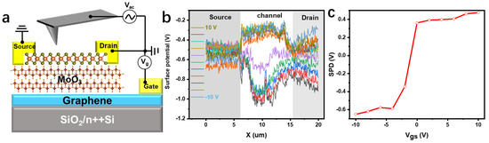
Figure 4.
(a) Schematic diagram of KPFM test structure. (b) Surface potential diagram at different gate voltages, the interval is 2 V. (c) Summary diagram of contact potential difference between electrode and MoS2 under different gate voltages.
2.4. Device Specific Performance Parameters
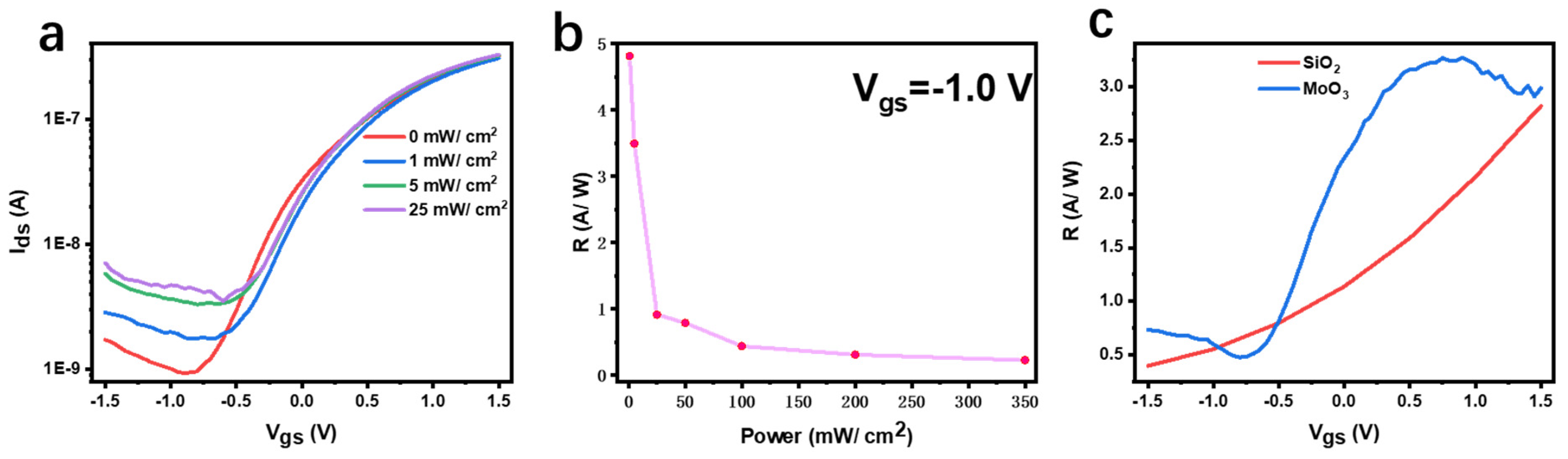
Furthermore, the photoelectric performance of the device is verified. We irradiated the entire surface of the device with a 405 nm laser, adjusted the different laser powers and tested whether the relationship between the source–drain current and the gate voltage would be changed compared with the dark state (Figure 5a). As can be seen from Figure 5a, the photoelectric response of the device is more obvious under the action of negative gate pressure. According to the following formula:
where is photoresponsivity, is the optical power density, is the effective area of the device, and denote the photocurrent and dark current, respectively.

Figure 5.
(a) Transfer curves of a 405 nm laser with a different light power in MoO3 medium. (b) The relationship between responsivity and optical power at the same gate voltage in MoO3 medium. (c) The relationship between the responsivity and gate voltage of the two media under the same light power (50 mW/cm2).
The highest responsivity of the device can be obtained as the power is 1 mW/cm2 in Figure 5b. Figure 5c summarizes the functional relationship between the responsivity of MoS2 on different substrates and the gate voltage. Since the difference between the photocurrent and dark current of MoS2/MoO3 is larger than that of MoS2/SiO2, by comparison, it is found that the responsivity of MoS2/MoO3 is significantly higher than that of MoS2/SiO2 under the same optical power, indicating that MoS2 on MoO3 substrate shows superior photoelectric performance.
3. Conclusions
We demonstrate that MoS2/MoO3 can effectively reduce the device operating voltage. The device exhibits a high on–off ratio (105), low SS (400 mV/dec), high electron mobility (85 cm2 V−1 s−1), low lag and high stability due to fewer surface defects. In addition to this, we obtained devices with higher electron mobility and a lower density of defect states, which favors smaller hysteresis voltage. Furthermore, the device is capable of significant response to visible light and the most responsivity is near 5 A/W. In general, this study proves that high-κ van der Waals MoO3 can be effectively applied to the gate dielectric layer to improve the photoelectric performance of the device.
4. Experimental Section
MoO3 Single Crystal Growth: We used the vapor deposition method, placed approximately 0.1 g of MoO3 powder in the center of the ark, and then placed the ark in the center of the tube furnace, continued to pass in the gas Ar at a rate of 100 sccm, and connected the gas outlet to the atmosphere. The heating started from room temperature (25 °C), 25 min to 780 °C, keeping warm for 1 min, then the heating tube was quickly removed, and the tube furnace was allowed to cool down rapidly, during which MoO3 nanosheets could be seen flying out and depositing on the silicon wafer approximately 10 cm away from the powder on the side near the gas outlet. This resulted in large-area MoO3 nanosheets.
Gr/MoO3/MoS2 Heterostructure Memory Devices Fabrication: We used the mechanical exfoliation method, used the layered structure of 2D materials, used tape to obtain thin-layer materials, and transferred the thin-layer materials to the same silicon wafer through PDMS. Figure S3 shows the transfer schematic diagram, and displays the transfer and stacking of Gr, MoO3 and MoS2 from left to right, respectively. Then, we used the flocculated crystals generated in the tube furnace during the growth of MoO3 nanosheets to cover the surface of the transistor part with the probes. The surface of the transistor is covered with gold by evaporation method, and the channel of the transistor can be obtained by removing the crystal. Finally, the device is obtained by drawing electrodes with a probe.
Device Characterization: AFM (NT-MDT NTEGRA) was used to characterize the change of surface morphology. The photoluminescence spectrum was measured using confocal Raman microscope (Horiba LabRAM HR Evolution Inc., Palaiseau, France). Semiconductor device parameter analyzer (FS-Pro, Primarius Electronic Technology, Beijing, China) was employed to characterize the electrical properties of the devices. Semiconductor lasers with a wavelength of 405 nm were used to study the photoresponse properties of the devices.
Supplementary Materials
The following supporting information can be downloaded at: https://www.mdpi.com/article/10.3390/ma15175859/s1, Figure S1. The detailed process of growing MoO3 nanosheets using vapor deposition method, the resulting nanosheets are shown in Figure 1b. Figure S2. I-V curve of MoO3. Figure S3. Gr/MoO3/MoS2 heterostructure transfer process.
Author Contributions
Conceptualization, J.W. and W.X.; methodology, J.W. and H.L.; software, J.W. and H.L.; formal analysis, X.H.; investigation, J.W., H.L., X.H., J.L. and Y.L.; resources, J.L.; data curation, J.W.; writing—original draft preparation, J.W. and H.L.; writing—review and editing, J.W. and H.L.; visualization, Y.L.; supervision, W.X. and P.L.; project administration, W.X. and P.L.; funding acquisition, W.X. All authors have read and agreed to the published version of the manuscript.
Funding
This work was supported by the National Natural Science Foundation of China (Grant Nos. 62174072), Guangdong Basic and Applied Basic Research Foundation (Grant No. 2019B151502049). W.X. also acknowledge the Guangzhou Key Laboratory of Vacuum Coating Technologies and New Energy Materials (No. 201605030008).
Conflicts of Interest
The authors declare no conflict of interest.
References
- Robertson, J.; Falabretti, B. Band offsets of high K gate oxides on III-V semiconductors. J. Appl. Phys. 2006, 100, 014111. [Google Scholar] [CrossRef]
- Javey, A.; Kim, H.; Brink, M.; Wang, Q.; Ural, A.; Guo, J.; McIntyre, P.; McEuen, P.; Lundstrom, M.; Dai, H. High-kappa dielectrics for advanced carbon-nanotube transistors and logic gates. Nat. Mater. 2002, 1, 241–246. [Google Scholar] [CrossRef] [PubMed]
- Gusev, E.P.; Cartier, E.; Buchanan, D.A.; Gribelyuk, M.; Copel, M.; Okorn-Schmidt, H.; D’Emic, C. Ultrathin high-K metal oxides on silicon: Processing, characterization and integration issues. Microelectron. Eng. 2001, 59, 341–349. [Google Scholar] [CrossRef]
- Wilk, G.D.; Wallace, R.M.; Anthony, J.M. High-κ gate dielectrics: Current status and materials properties considerations. J. Appl. Phys. 2001, 89, 5243–5275. [Google Scholar] [CrossRef]
- Wang, Y.; Chhowalla, M. Making clean electrical contacts on 2D transition metal dichalcogenides. Nat. Rev. Phys. 2022, 4, 101–112. [Google Scholar] [CrossRef]
- Chourasia, N.K.; Sharma, A.; Acharya, V.; Pal, N.; Biring, S.; Pal, B.N. Solution processed low band gap ion-conducting gate dielectric for low voltage metal oxide transistor. J. Alloys Compd. 2019, 777, 1124–1132. [Google Scholar] [CrossRef]
- Ganapathi, K.L.; Bhat, N.; Mohan, S. Optimization and integration of ultrathin e-beam grown HfO2 gate dielectrics in MoS2 transistors. J. Phys. D Appl. Phys. 2021, 54, 445302. [Google Scholar] [CrossRef]
- Cho, A.J.; Yang, S.; Park, K.; Namgung, S.D.; Kim, H.; Kwon, J.Y. Multi-Layer MoS2 FET with Small Hysteresis by Using Atomic Layer Deposition Al2O3 as Gate Insulator. ECS Solid State Lett. 2014, 3, Q67–Q69. [Google Scholar] [CrossRef]
- Ahmed, F.; Heo, S.; Yang, Z.; Ali, F.; Ra, C.H.; Lee, H.-I.; Taniguchi, T.; Hone, J.; Lee, B.H.; Yoo, W.J. Dielectric Dispersion and High Field Response of Multilayer Hexagonal Boron Nitride. Adv. Funct. Mater. 2018, 28, 1804235. [Google Scholar] [CrossRef]
- Liu, K.; Jin, B.; Han, W.; Chen, X.; Gong, P.; Huang, L.; Zhao, Y.; Li, L.; Yang, S.; Hu, X.; et al. A wafer-scale van der Waals dielectric made from an inorganic molecular crystal film. Nat. Electron. 2021, 4, 906–913. [Google Scholar] [CrossRef]
- Khandare, L.; Terdale, S.S.; Late, D.J. Ultra-fast α-MoO3 nanorod-based Humidity sensor. Adv. Device Mater. 2016, 2, 15–22. [Google Scholar] [CrossRef]
- Holler, B.A.; Crowley, K.; Berger, M.H.; Gao, X.P.A. 2D Semiconductor Transistors with Van der Waals Oxide MoO3 as Integrated High-κ Gate Dielectric. Adv. Electron. Mater. 2020, 6, 2000635. [Google Scholar] [CrossRef]
- Bhattacharjee, S.; Ganapathi, K.L.; Mohan, S.; Bhat, N. A sub-thermionic MoS2 FET with tunable transport. Appl. Phys. Lett. 2017, 111, 163501. [Google Scholar] [CrossRef]
- Chau, T.K.; Phan, T.L.; Park, N.; Na, J.; Suh, D. Distinctive Photo-Induced Memory Effect in Heterostructure of 2D Van Der Waals Materials and Lanthanum Aluminate. Adv. Opt. Mater. 2022, 10, 2200124. [Google Scholar] [CrossRef]
- Guo, Y.; Robertson, J. Origin of the high work function and high conductivity of MoO3. Appl. Phys. Lett. 2014, 105, 222110. [Google Scholar] [CrossRef]
- Peelaers, H.; Chabinyc, M.L.; Van de Walle, C.G. Controlling n-Type Doping in MoO3. Chem. Mater. 2017, 29, 2563–2567. [Google Scholar] [CrossRef]
- Meyer, J.; Kidambi, P.R.; Bayer, B.C.; Weijtens, C.; Kuhn, A.; Centeno, A.; Pesquera, A.; Zurutuza, A.; Robertson, J.; Hofmann, S. Metal oxide induced charge transfer doping and band alignment of graphene electrodes for efficient organic light emitting diodes. Sci. Rep. 2014, 4, 5380. [Google Scholar] [CrossRef]
- Wang, Y.; Du, X.; Wang, J.; Su, M.; Wan, X.; Meng, H.; Xie, W.; Xu, J.; Liu, P. Growth of Large-Scale, Large-Size, Few-Layered alpha-MoO3 on SiO2 and Its Photoresponse Mechanism. ACS Appl. Mater. Interfaces 2017, 9, 5543–5549. [Google Scholar] [CrossRef] [PubMed]
- Bai, J.; Huang, Y. Fabrication and electrical properties of graphene nanoribbons. Mater. Sci. Eng. R Rep. 2010, 70, 341–353. [Google Scholar] [CrossRef]
- Ferrari, A.C.; Meyer, J.C.; Scardaci, V.; Casiraghi, C.; Lazzeri, M.; Mauri, F.; Piscanec, S.; Jiang, D.; Novoselov, K.S.; Roth, S.; et al. Raman spectrum of graphene and graphene layers. Phys. Rev. Lett. 2006, 97, 187401. [Google Scholar] [CrossRef] [Green Version]
- Li, H.; Zhang, Q.; Yap, C.C.R.; Tay, B.K.; Edwin, T.H.T.; Olivier, A.; Baillargeat, D. From Bulk to Monolayer MoS2: Evolution of Raman Scattering. Adv. Funct. Mater. 2012, 22, 1385–1390. [Google Scholar] [CrossRef]
- Seguin, L.; Figlarz, M.; Cavagnat, R.; Lassègues, J.C. Infrared and Raman spectra of MoO3 molybdenum trioxides and MoO3 · xH2O molybdenum trioxide hydrates. Spectrochim. Acta Part A Mol. Biomol. Spectrosc. 1995, 51, 1323–1344. [Google Scholar] [CrossRef]
- Crowley, K.; Ye, G.; He, R.; Abbasi, K.; Gao, X.P. α-MoO3 as a conductive 2D oxide: Tunable n-type electrical transport via oxygen vacancy and fluorine doping. ACS Appl. Nano Mater. 2018, 1, 6407–6413. [Google Scholar] [CrossRef]
- Liu, D.; Guo, Y.; Fang, L.; Robertson, J. Sulfur vacancies in monolayer MoS2 and its electrical contacts. Appl. Phys. Lett. 2013, 103, 183113. [Google Scholar] [CrossRef]
- Srivastava, A.; Fahad, M.S. Vertical MoS2/hBN/MoS2 interlayer tunneling field effect transistor. Solid State Electron. 2016, 126, 96–103. [Google Scholar] [CrossRef]
- Hu, Y.; Jiang, H.; Lau, K.M.; Li, Q. Chemical vapor deposited monolayer MoS2 top-gate MOSFET with atomic-layer-deposited ZrO2 as gate dielectric. Semicond. Sci. Technol. 2018, 33, 045004. [Google Scholar] [CrossRef]

Publisher’s Note: MDPI stays neutral with regard to jurisdictional claims in published maps and institutional affiliations. |
© 2022 by the authors. Licensee MDPI, Basel, Switzerland. This article is an open access article distributed under the terms and conditions of the Creative Commons Attribution (CC BY) license (https://creativecommons.org/licenses/by/4.0/).