Abstract
In this work, the resistive switching behavior of bilayer ZnO/Al2O3-based resistive-switching random access memory (RRAM) devices is demonstrated. The polycrystalline nature of the ZnO layer confirms the grain boundary, which helps easy oxygen ion diffusion. Multilevel resistance states were modulated under DC bias by varying the current compliance from 0.1 mA to 0.8 mA, the SET operations where the low resistance state of the memristor device was reduced from 25 kΩ to 2.4 kΩ. The presence of Al2O3 acts as a redox layer and facilitates oxygen vacancy exchange that demonstrates stable gradual conductance change. Stepwise disruption of conductive filaments was monitored depending on the slow DC voltage sweep rate. This is attributed to the atomic scale modulation of oxygen vacancies with four distinct reproducible quantized conductance states, which shows multilevel data storage capability. Moreover, several crucial synaptic properties such as potentiation/depression under identical presynaptic pulses and the spike-rate-dependent plasticity were implemented on ITO/ZnO/Al2O3/TaN memristor. The postsynaptic current change was monitored defining the long-term potentiation by increasing the presynaptic stimulus frequency from 5 Hz to 100 Hz. Moreover, the repetitive pulse voltage stimulation transformed the short-term plasticity to long-term plasticity during spike-number-dependent plasticity.
1. Introduction
Emulating brain-inspired synaptic devices has recently attracted attention as a potential application in neuromorphic computing systems [1,2,3,4]. In this context, resistive random access memories (RRAM) with a simple metal–insulator–metal structure have been studied due to their low power consumption, high speed, and high-density memory storage ability [5,6]. However, stable gradual conductance change due to controlled movement of oxygen vacancies is the challenge for integrating memristor in simulating the synaptic function. ZnO and Al2O3 have shown excellent electrical and optical properties and have been studied successfully in resistive switching. The crystallinity and oxygen content of reactively sputtered ZnO film was found to be largely controlled by the O2/Ar ratio during sputtering. Further, it influences the oxygen vacancy (VO) formations during the electroforming of conductive filaments [7]. Jing et al. and Gu et al., have explained the mechanism [8,9]. They have shown that the oxygen vacancy defect states and are originated by the O-deficient Zn orbitals, and the electron and hole injection under the electric field in the ZnO layer controls the formation and rupture of the oxygen-vacancy-related conductive filaments. So, the diffusion of oxygen vacancies by an external electric field controls the resistive switching in the memristor [8]. In this context, Gul et al. introduced an oxygen deficient (ZnO1−x) layer intentionally by controlling the O2 flow during sputtering between two ZnO layers [10]. However, the filamentary bipolar switching shows a very low ON/OFF ratio. On the other hand, SET and RESET mechanisms were modulated by the external doping of Li and Cu doped ZnO [11,12] although the RESET switching behaviors observed in these cases were stepwise and mostly abrupt. Cobalt dopants in ZnO demonstrated improved resistive switching with a comparatively higher memory window and stable endurance properties, where Co-dopants suppressed uncontrolled oxygen vacancy formations [13]. Recently it was demonstrated that Al2O3 is a stable electrical insulator with a large bandgap and low leakage characteristics, which benefits from reliable and reproducible switching characteristics [14,15,16,17]. The Al2O3 interfacial layer plays a significant role in controlling multilevel storage and oxygen vacancies at the oxide/oxide interface [18]. The interlayer formation between the Al2O3/oxide interface plays an important role, and the migration of oxygen ions controls the redox reactions by localizing the formation and rupture of the conductive filaments [14]. Previous reports show that buffer Al2O3 introduction with the ZnO layer has improved unipolar resistive switching with a modified memory window [19]. Moreover, inserting the semiconducting layer with an Al2O3 resistive switching device can be beneficial for attaining low-voltage bipolar memory properties [20]. According to the previous study, the grain boundary is present in the polycrystalline ZnO layer, where loss of oxygen vacancy can be reduced, and a stable switching performance can be achieved by introducing a thin Al2O3 layer [21]. Wang et al. described the Al2O3/ZnO bilayer RRAM structure using the ALD technique where both SET and RESET processes were found to be abrupt [22]. On the other hand, Lekshmi et al. used ALD deposited Al2O3/ZnO bilayer memristor with large variability in cycle-to-cycle switching with ON/OFF ratio less than 10 [23]. Tri-layer Al2O3/ZnO/Al2O3 has also been used as a switching layer with uni-polar switching using non-reactive Pt electrodes [19]. Tri-layer memristor was also reported by Kumar et al. where the endurance of bi-polar resistive witching was improved [21]. In earlier reports on Al2O3/ZnO bilayer and Al2O3/ZnO/Al2O3 tri-layer based memristors, the synaptic behavior was not studied in detail, an essential characteristic of neuroplasticity.
A detailed study on gradual conductance change under DC and pulse conditions for short-term and long-term memory behaviors is critically needed for future synaptic device applications. So, this work is focused on the various essential synaptic properties inserting an Al2O3 interfacial layer between ZnO and the TaN electrode in ITO/ZnO/Al2O3/TaN. The ZnO layer was deposited by RF sputter using the pure Zn target and O2+Ar gas flow. The sputtered ZnO/Al2O3 interface controls the gradual resistive switching in the memristor. Stable resistive switching and synaptic properties show that gradual conductance change can be achieved by applying electrical stimuli. The memristor can be successfully mimicked as a biological synapse with basic function short-term plasticity (STP), long-term plasticity (LTP), spike rate dependent plasticity (SRDP), spike number dependent plasticity (SNDP), and paired-pulse facilitation (PPF).
2. Materials and Methods
Bottom electrode TaN was prepared by sputtering on Si/SiO2 substrate with a thickness ~100 nm using the pure TaN target with a Ar flow of 20 sccm. Surface contamination was removed by sequential ultrasonic cleaning with acetone, isopropyl alcohol, and DI water. After cleaning of the TaN surface, the first switching layer of ~3 nm Al2O3 was deposited using an atomic layer deposition (ALD) system with Al metal precursors as trimethylaluminum (TMA) and H2O as ALD oxidant at a substrate temperature of 280 °C. To achieve the target thickness, the recipe of Al2O3 deposition (total 26 cycles) for 1 cycle was kept as: TMA 0.2 s/Purge 15 s/H2O 0.2 s/Purge 15 s. After that, the ZnO layer (~30 nm) was deposited by radio frequency (RF) sputtering system at the 10−3 Torr working gas pressure. The gas mixture of Ar + O2 at a ratio of 8:12 sccm was used with RF power of 80 W. Finally, 100 μm × 100 μm square patterns were formed through a photo-lithography process. Indium tin oxide (ITO) was deposited (Ar, 8 sccm and RF 60 W) from an ITO target (90:10 wt %) followed by the lift-off process to fabricate the ITO/ZnO/Al2O3/TaN memristor. The microstructure of the ITO/ZnO/Al2O3/TaN device was analyzed by the high-resolution transmission electron microscopy (JEOL JEM-F200) along with energy-dispersive x-ray spectroscopy (EDS). Using the Keithley 4200 SCS semiconductor parameter analyzer and 4225-PMU pulse module, DC resistive switching performances and presynaptic pulse-induced synaptic characteristics were evaluated.
3. Results and Discussion
3.1. Structural Characterization
The structural properties and thickness of each layer of fabricated ITO/ZnO/Al2O3/TaN memristor were analyzed by high-resolution transmission electron microscopy (HRTEM) and energy-dispersive X-ray spectroscopy (EDS) line profile. HRTEM shows the switching layer consists of a polycrystalline 30 nm ZnO, and an amorphous 3 nm Al2O3 bilayer, as shown in Figure 1a,b. A magnified TEM image shows a polycrystalline nature of the ZnO layer which is suitable for electroforming conductive filaments, whereas the amorphous Al2O3 helps resistive switching characteristics. The EDS line scan atomic % of N, O, Ta, Al, In, Sn, and Zn elements was present in the structure which further confirms the presence of each layer in the fabricated memristor as shown in Figure 1c.
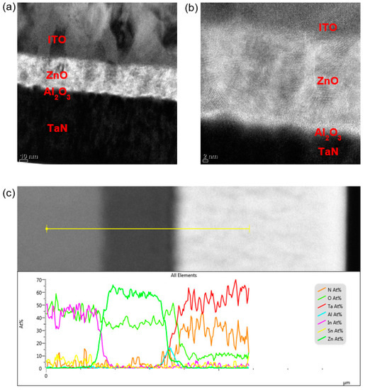
Figure 1.
(a,b) HRTEM image of pristine ITO/ZnO/Al2O3/TaN resistive switching device; (c) EDS line profile of atomic % of N, O, Ta, Al, In, Sn, and Zn scanned from top to bottom electrodes.
3.2. Electroforming and Bipolar Resistive Switching of ITO/ZnO/Al2O3/TaN Device
Bipolar resistive switching was achieved in the ITO/ZnO/Al2O3/TaN memristor after the electroforming of conductive filaments (CFs) due to the creation of oxygen vacancies under external electric field. In this experiment, electroforming of several memristors were monitored at the current compliance of 10 µA as shown in the Figure 2a. Lower current compliance was selected for protecting the memristor from strong filament formation that cause hard breakdown of the switching layer. The variation of the electroforming voltage may be due to the large area of the device, which forms a different number of CFs under the electric field. The generation of oxygen ions and oxygen vacancies (VO) during the external field was further examined by the ramp voltage stress (RVS), where the maximum sweep voltage was increased slowly stepwise by +0.3 V as shown in Figure 2b [24]. Figure 2b shows that the positive charge build-up occurs due to VO+ formation during RVS and an eventual SBD due to the CFs connecting the top and bottom electrodes. The initial jump in I–V characteristics during RVS at the voltage range of +6.5 to +7.8 V may be due to the presence of polycrystalline ZnO where the strong filament forms easily due to the grain boundary, which provides oxygen vacancies diffusion much easier [25,26]. At higher RVS, the oxygen vacancy creation was slower, possibly due to the Al2O3 layer and a final soft breakdown, as shown in Figure 2b. Figure 2c shows 200 DC cycles of bipolar resistive switching properties for ITO/ZnO/Al2O3/TaN memristor, which shows stable endurance properties, and cycle-to-cycle ION/IOFF ratio variations are pretty small. The presence of crystalline ZnO in the switching layer forms a strong filament during electroforming due to the easy movements of oxygen ions [21]. According to Kumar et al., oxygen vacancy in ZnO layers is four times higher than Al2O3 layers, which play a key role in stabilizing the CFs size and shape [21]. So, when positive voltage is applied to the top electrode during electroforming, thicker cylindrical CFs form inside the ZnO layer. Close to the bottom electrode, Al2O3 contains thin filaments. During the RESET process at the negative top electrode bias, oxygen ions drift from the TaN electrode (due to the presence of the TaOxNy interlayer) easily. The oxygen ions recombine with oxygen vacancy inside the Al2O3 layer and rupture the filaments (RESET) due to the presence of the weakest part located at the interface of the ZnO/Al2O3. So, the thin layer of Al2O3 can stabilize the filament formation and rupture during resistive switching. In the cyclic steps during SET operation, the oxygen ions are again depleted (O-vacancy creation) due to the application of positive bias at the top electrode. The schematic illustration of the SET and RESET operation of the bipolar resistive switching is shown in Figure 2d. Stable DC switching properties of multiples devices are presented in Figure S1 (supplementary materials) which confirm the device-to-device stable variability. During the RESET operation, multiple memory states are achieved at a very slow rate of sweep voltage at −0.005 V/0.5 s as shown in Figure 2e. The stepwise current change is analogous due to the quantum conductance change reported earlier [27,28,29]. So, during the RESET process (25 cycles), the currents reduce from la ow resistance state (LRS) to a high resistance state (HRS) due to the progressive reduction in CFs size behaving as quantum conductance behavior. As shown in Figure 2d, the clear four conductance states indicate multiple stable quantum states suitable for synaptic applications described later in the section below.
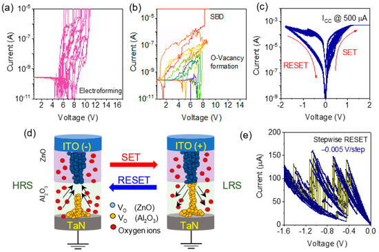
Figure 2.
(a) Electroforming behavior of ITO/ZnO/Al2O3/TaN memristor with current compliance of 10 µA; (b) charge trapping and O-vacancy formation at increasing ramp voltage stress; (c) bipolar resistive switching properties of the memristor at the current compliance of 10 µA; (d) schematic illustration of formation and rupture of CFs during the SET and RESET process at the ZnO/Al2O3 interface; (e) 50 cycles of multiple RESET characteristics at a very low sweep rate of −0.005 V/0.5 s show the quantized conductance states.
In the ITO/ZnO/Al2O3/TaN memristor, multiple resistance states were achieved by controlling the current compliance (ICC) during the SET process and at a RESET voltage of −1.7 V as shown in Figure 3a,b. Varying the current compliance from 0.1 mA to 0.8 mA, the LRS was changed from 25 kΩ to 2.4 kΩ as depicted in Figure 3b. Resistance states were stable up to 100 DC cycles, indicating the multilevel memory capability of ITO/ZnO/Al2O3/TaN memristor. The mechanism of multilevel states achieved due to increasing ICC was attributed to the enhancement of the CFs diameter, which caused multiple LRS [3,30]. Figure 3c illustrates filament size modifications under HRS and multiple resistance at LRS1 to LRS 5. So, the control of oxygen vacancy creation inside the Al2O3 layer during resistive switching by modifying the DC electrical parameter confirms the feasible application of ITO/ZnO/Al2O3/TaN memristor for the synaptic devices. Device-to-device endurance properties are plotted in Figure 3d, confirming that the RON/ROFF ratio is always >10, suitable for memristor applications.
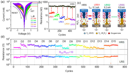
Figure 3.
(a) Resistive switching behavior of ITO/ZnO/Al2O3/TaN memristor with varied current compliance at the SET process; (b) distribution of HRS and multiple LRS with 100 cycles endurance each; (c) filament growth model for oxygen vacancy formation inside ZnO/Al2O3 switching layer and increasing CFs diameter during multiple LRS; (d) endurance characteristics of 15 individual memristor shows an ION/IOFF ratio of >10.
3.3. Synaptic Characteristics under Identical Pulse Sequence
Furthermore, synaptic properties were emulated for ITO/ZnO/Al2O3/TaN memristor with identical pulse sequences. Gradual conductance modulation under electrical pulses is an essential synaptic property for neuromorphic applications. A continuous tunable synaptic weight change was observed during potentiation and depression with an identical pulse amplitude of +0.7 V/1 ms and −0.9 V/1 ms correspondingly, as shown in Figure 4a. A fast transition at the first pulse was observed, followed by a gradual change in synaptic weight (current) in both cases similar to the previous reports [31,32]. Although in case of the depression process the rupture of CFs is faster than formation, five consecutive potentiation/depression cycles indicated the stable and reproducible synaptic properties of the ITO/ZnO/Al2O3/TaN memristor. A normalized conductance vs. pulse number is plotted in Figure 4b for the bilayer device. From multiple cycles, the synaptic weight change (Δw) was fitted, and the nonlinearity factors were obtained by the Equation [32]:
where GHRS and GLRS are the conductance at HRS and LRS, w is varied from 0 to 1, and α is the nonlinearity factor for potentiation and depression. Nonlinearity at potentiation and depression was found to be αp~1.8 and αd~−0.15, respectively. The transition from synaptic short-term plasticity (STP) to long-term plasticity (LTP) was further monitored by varying the spike number from 1 to 10 with a pulse amplitude of +0.85 V/50 µs as shown in Figure 4c. As shown here, after two spikes, the base voltage (+0.2 V) was recovered, suggesting STP behavior. As shown in Figure 4c, after the application of five successive pulses, a transition from STP to LTP was observed due to the generation of continuous neutral [33]. A similar phenomenon was also confirmed by Luo et al. [34]. However, during spike-number-dependent plasticity (SNDP), the effect of repetitive pulse shows that an eventual LTP behavior can be achieved after 10 stimuli [35]. Repeated pulse strengthens the CFs inside the switching layer through rehearsal, which emulates the biological synaptic behavior as mentioned by Kim et al. [1]. The SNDP ratio An/A1 due to the change of excitatory postsynaptic current (EPSC) was increased from 1.1 to 1.25 after applying 1 to 10 spikes, as shown in Figure 4d.
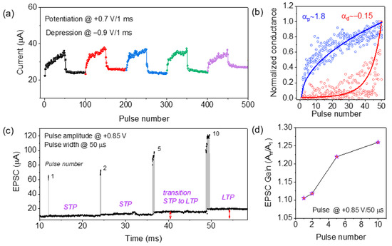
Figure 4.
(a) Five cycles of potentiation/depression were obtained with 50 identical pulse trains of +0.7 V/1 ms and −0.9 V/1 ms correspondingly; (b) linearity factors of potentiation/depression were calculated using Equation (1); (c) pulse-number-dependent STP to LTP transition with a pulse amplitude of +0.85 V/1 ms; (d) EPSC gain from the ratio of An/A1 is plotted.
3.4. Pulse-Frequency-Dependent and Experience-Dependent Synaptic Properties
In neuroscience, spike-rate-dependent plasticity (SRDP) is another essential synaptic function for modifications of memory learning processes that describes the synaptic plasticity dependency on the spike frequency [36,37,38,39]. Figure 5a illustrates the frequency-dependent EPSC response ranges from 5 Hz to 100 Hz with an amplitude of +0.85 V/200 µs in the short-term memory (STM) mode. Each pulse stimulus contains 20 identical pulses with different pulse delay. Current increases significantly at the higher frequencies, whereas the current increment is reduced at the comparatively lower frequency. At the lower frequency of 5 Hz to 10 Hz, the longer recombination time of oxygen vacancies and oxygen ions current is relaxed and tends to reach equilibrium [39]. The EPSC gain is further plotted against the spike frequency in Figure 5b. Synaptic weight change A20/A1 (A20 and A1 refer to the current amplitude at the 20th and 1st pulse) clearly depicts that significant potentiation behavior occurred at the higher frequencies. So, the frequency-dependent synaptic weight change in ITO/ZnO/Al2O3/TaN memristor can mimic the high-pass filter where synaptic functions enhance due to high-frequency input pulse frequency. Experience- or history-dependent plasticity was also emulated on the memristor by applying high- to low-frequency spike trains [36,40]. Series of pulse trains with different pulse frequencies were applied to ITO/ZnO/Al2O3/TaN memristor with amplitude of +0.9 V/200 µs, and the change in current was observed as shown in Figure 5c,d. The postsynaptic currents increase (learning process) due to the spike train frequency of 5 Hz and 10 Hz at the first stage, whereas at the second stage at spike train frequency of 2 Hz, the current increment or even decreasing trends (forgetting process) were observed. So, the potentiation and depression of synaptic weights are controlled by the pulse train frequency without the application of opposite polarity voltage, which mimics a bio-synapse [37,38]. Similar behavior was reported by Khanas et al. and Yan et al. previously [38,41]. So, ITO/ZnO/Al2O3/TaN memristor shows the frequency-dependent synaptic weight change, and the potentiation/depression synaptic function can be emulated depending on the history of the frequency.
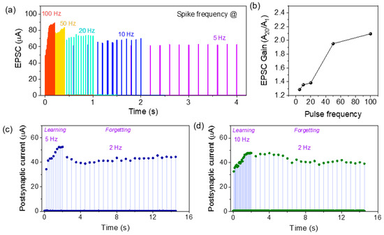
Figure 5.
(a) Current response of ITO/ZnO/Al2O3/TaN memristor with consecutive 20 pulse train at the frequency ranges from 5 Hz to 100 Hz with an amplitude of +0.85 V/200 µs; (b) frequency-dependent EPSC gain of the memristor; (c,d) postsynaptic current response shows STP effect at decreasing frequency with the same pulse amplitude of +0.9 V/200 µs.
3.5. Paired-Pulse Facilitation(PPF) Emulation
The short-term synaptic plasticity phenomenon was mimicked for the ITO/ZnO/Al2O3/TaN memristor with PPF behavior for excitatory response [42,43]. The excitatory postsynaptic current (EPSC) triggered by the second synaptic spike increased compared to the first one during the paired pre-spike pulse signals, as shown in Figure 6a. The EPSC increased sharply due to the presynaptic voltage spike of +0.9 V/500 µs and tended to decay after the first pulse [44]. After applying the successive second pulse, triggered EPSC was found larger than the first one. Depending on the interval time (Δt) of the two pulses, the magnitude of the postsynaptic current at the second pulse increased correspondingly [43]. So, depending on the time interval, the created oxygen vacancies inside the switching layer diffuse back and recombined with oxygen ions. At the shorter interval of 1 ms between two pulses, the recombination process was less compared to the larger pulse interval at 10 ms, and as a consequence, the PPF response increased at the shorter interval. Due to the short interval between the first and second presynaptic spike, the total amount of residual oxygen vacancies increased due to less recombination time. The PPF index A2/A1 × 100% as a function of Δt is plotted in Figure 6b [42]. As shown in Figure 6b, larger delay time induces a Vo+ and O− recombination, which results in a decreased PPF index. The experimental data was fitted with the decay factor to determine the relaxation time constant by Equation (2):
where Δt is the pre-spike interval time, τ1 and τ2 are the characteristic relaxation time, and C1 and C1 are the initial facilitation magnitudes [45]. After fitting with experimental data, the value of τ1 and τ2 was found 6.6 ms and 885 ms, respectively. So, in this study, the gradual change in PPF exponential decay response mimics the biological synaptic properties analogous to the neurotransmitter. Table 1 illustrates the comparison of experimental DC electrical parameters and synaptic properties such as VSET, VRESET, ON/OFF ratio, and switching type of existing various stacks of ZnO and the Al2O3-based memristor. It can be seen that ITO/ZnO/Al2O3/TaN is comparable to the DC characteristics of previously reported memristors. Comparing the postsynaptic current changes in the case of sputtered-ZnO/ALD-Al2O3 stacks in the present experiment is advantageous regarding various synaptic characteristics.
PPF = C1 exp(−Δt/τ1) + C1 exp(−Δt/τ2)
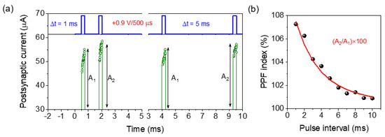
Figure 6.
Paired-pulse facilitation short-term memory synaptic function of the ITO/ZnO/Al2O3/TaN memristor device; (a) post-synaptic current response at the pair pulse of +0.9 V/500 µs with a time interval (Δt) of 1 ms and 5 ms; (b) experimental PPF index calculated from output current of first and second pulse as (A2/A1) × 100% along with fitted curve using Equation (2) at the pre-spike time interval of 1 ms to 10 ms.

Table 1.
Comparison of resistive switching and synaptic properties of ZnO and the ZnO/Al2O3-based memristor.
4. Conclusions
The resistive switching characteristics and synaptic properties of the ZnO/Al2O3 bilayer devices were investigated in detail. The regular grain size of the sputtered deposited ZnO layer and a thin atomic deposited Al2O3 layer help enhance synaptic properties gradual formation and rupture of the conductive filaments in the ZnO/Al2O3 interface. Oxygen ions movement due to the presence of the Al2O3 layer facilitates the controlled formation and recombination of oxygen vacancy near the ZnO/Al2O3 interface. Multistate memory storage was observed by changing the DC SET current compliance with stable endurance properties. The slow voltage sweep rate at 0.005 V/0.5 s during the RESET process shows the quantized conductance characteristics with stepwise change in current. Achievement of QC-states primarily in the current memristor shows potential applications for high-density storage. Essential synaptic functions, such as potentiation/depression, SRDP, SNDP, and PPF learning rules, are demonstrated on an ITO/ZnO/Al2O3/TaN device that emulates the biological synapse. Experimental evidence of STP to LTP transition characteristics by frequent presynaptic pulse repetition was observed. Thus, promising electrical properties of the memristor suggest future applications in neuromorphic devices.
Supplementary Materials
The following supporting information can be downloaded at: https://www.mdpi.com/article/10.3390/ma15196663/s1, Figure S1: Bipolar resistive switching performances of 16 individual ITO/ZnO/Al2O3/TaN memristor.
Author Contributions
Conceptualization, experiments and data analysis, writing, C.M.; experiments, J.P. and M.I.; review and editing, D.H.K. and S.K. All authors have read and agreed to the published version of the manuscript.
Funding
This work was supported in part by the National Research Foundation of Korea (NRF) grant funded in part by the Korean Government (MSIT) (No. 2016R1A5A1012966) and Korea Institute of Energy Technology Evaluation and Planning (KETEP) grant funded by the Korea government (MOTIE) under Grant 20224000000020.
Institutional Review Board Statement
Not applicable.
Informed Consent Statement
Not applicable.
Data Availability Statement
Not applicable.
Conflicts of Interest
The authors declare no conflict of interest.
References
- Kim, M.K.; Lee, J.S. Short-Term Plasticity and Long-Term Potentiation in Artificial Biosynapses with Diffusive Dynamics. ACS Nano 2018, 12, 1680–1687. [Google Scholar] [CrossRef]
- Ambrosi, E.; Bricalli, A.; Laudato, M.; Ielmini, D. Impact of oxide and electrode materials on the switching characteristics of oxide ReRAM devices. Faraday Discuss. 2019, 213, 87–98. [Google Scholar] [CrossRef] [PubMed]
- Ielmini, D. Resistive switching memories based on metal oxides: Mechanisms, reliability and scaling. Semicond. Sci. Technol. 2016, 31, 063002. [Google Scholar] [CrossRef]
- Sun, B.; Guo, T.; Zhou, G.; Ranjan, S.; Jiao, Y.; Wei, L.; Zhou, Y.N.; Wu, Y.A. Synaptic devices based neuromorphic computing applications in artificial intelligence. Mater. Today Phys. 2021, 18, 100393. [Google Scholar] [CrossRef]
- Yu, S.; Gao, B.; Fang, Z.; Yu, H.; Kang, J.; Wong, H.S.P. A low energy oxide-based electronic synaptic device for neuromorphic visual systems with tolerance to device variation. Adv. Mater. 2013, 25, 1774–1779. [Google Scholar] [CrossRef]
- Moon, K.; Lim, S.; Park, J.; Sung, C.; Oh, S.; Woo, J.; Lee, J.; Hwang, H. RRAM-based synapse devices for neuromorphic systems. Faraday Discuss. 2019, 213, 421–451. [Google Scholar] [CrossRef]
- Camacho-Berríos, A.A.; Pantojas, V.M.; Otaño, W. Reactive sputtered ZnO thin films: Influence of the O2/Ar flow ratio on the oxygen vacancies and paramagnetic active sites. Thin Solid Film. 2019, 692, 063002. [Google Scholar] [CrossRef]
- Zhao, J.; Dong, J.Y.; Zhao, X.; Chen, W. Role of oxygen vacancy arrangement on the formation of a conductive filament in a Zno thin film. Chin. Phys. Lett. 2014, 31, 3–6. [Google Scholar] [CrossRef]
- Gu, T. Metallic filament formation by aligned oxygen vacancies in ZnO-based resistive switches. J. Appl. Phys. 2014, 115, 203707. [Google Scholar] [CrossRef]
- Gul, F.; Efeoglu, H. ZnO and ZnO1−x based thin film memristors: The effects of oxygen deficiency and thickness in resistive switching behavior. Ceram. Int. 2017, 43, 10770–10775. [Google Scholar] [CrossRef]
- Lin, C.C.; Tang, J.F.; Su, H.H.; Hong, C.S.; Huang, C.Y.; Chu, S.Y. Multi-step resistive switching behavior of Li-doped ZnO resistance random access memory device controlled by compliance current. J. Appl. Phys. 2016, 119, 244506. [Google Scholar] [CrossRef]
- Xiao, J.; Herng, T.S.; Ding, J.; Zeng, K. Resistive switching behavior in copper doped zinc oxide (ZnO:Cu) thin films studied by using scanning probe microscopy techniques. J. Alloys Compd. 2017, 709, 535–541. [Google Scholar] [CrossRef]
- Simanjuntak, F.M.; Prasad, O.K.; Panda, D.; Lin, C.A.; Tsai, T.L.; Wei, K.H.; Tseng, T.Y. Impacts of Co doping on ZnO transparent switching memory device characteristics. Appl. Phys. Lett. 2016, 108, 3515–3520. [Google Scholar] [CrossRef]
- Wang, L.G.; Qian, X.; Cao, Y.Q.; Cao, Z.Y.; Fang, G.Y.; Li, A.D.; Wu, D. Excellent resistive switching properties of atomic layer-deposited Al2O3/HfO2/Al2O3 trilayer structures for non-volatile memory applications. Nanoscale Res. Lett. 2015, 10, 135. [Google Scholar] [CrossRef] [PubMed]
- Banerjee, W.; Xu, X.; Lv, H.; Liu, Q.; Long, S.; Liu, M. Variability improvement of TiOx/Al2O3 bilayer nonvolatile resistive switching devices by interfacial band engineering with an ultrathin Al2O3 dielectric material. ACS Omega 2017, 2, 6888–6895. [Google Scholar] [CrossRef] [PubMed]
- Mahata, C.; Lee, C.; An, Y.; Kim, M.H.; Bang, S.; Kim, C.S.; Ryu, J.H.; Kim, S.; Kim, H.; Park, B.G. Resistive switching and synaptic behaviors of an HfO2/Al2O3 stack on ITO for neuromorphic systems. J. Alloys Compd. 2020, 826, 154434. [Google Scholar] [CrossRef]
- Chen, L.; Xu, Y.; Sun, Q.-Q.; Liu, H.; Gu, J.-J.; Ding, S.-J.; Zhang, D.W. Highly Uniform Bipolar Resistive Switching With Al2O3 Buffer Layer in Robust NbAlO-Based RRAM. IEEE Electron Device Lett. 2010, 31, 356–358. [Google Scholar] [CrossRef]
- Song, W.; Wang, W.; Lee, H.K.; Li, M.; Zhuo, V.Y.-Q.; Chen, Z.; Chui, K.J.; Liu, J.-C.; Wang, I.-T.; Zhu, Y.; et al. Analog switching characteristics in TiW/Al2O3/Ta2O5/Ta RRAM devices. Appl. Phys. Lett. 2019, 115, 133501. [Google Scholar] [CrossRef]
- Qiao, Q.; Xu, D.; Li, Y.W.; Zhang, J.Z.; Hu, Z.G.; Chu, J.H. Detection of resistive switching behavior based on the Al2O3/ZnO/Al2O3 structure with alumina buffers. Thin Solid Film. 2017, 623, 8–13. [Google Scholar] [CrossRef]
- Park, J.; Huh, D.; Son, S.; Kim, W.; Ju, S.; Lee, H. Transparent, Flexible, and Low-Operating-Voltage Resistive Switching Memory Based on Al2O3/IZO Multilayer. Glob. Chall. 2022, 6, 2100118. [Google Scholar] [CrossRef]
- Kumar, D.; Chand, U.; Wen Siang, L.; Tseng, T.-Y. High-Performance TiN/Al2O3/ZnO/Al2O3/TiN Flexible RRAM Device With High Bending Condition. IEEE Trans. Electron Devices 2020, 67, 493–498. [Google Scholar] [CrossRef]
- Wang, D.T.; Dai, Y.W.; Xu, J.; Chen, L.; Sun, Q.Q.; Zhou, P.; Wang, P.F.; Ding, S.J.; Zhang, D.W. Resistive Switching and Synaptic Behaviors of TaN/Al2O3/ZnO/ITO Flexible Devices with Embedded Ag Nanoparticles. IEEE Electron Device Lett. 2016, 37, 878–881. [Google Scholar] [CrossRef]
- Arya Lekshmi, J.; Nandha Kumar, T.; Jinesh, K.B. The effect of the top electrode on the switching behavior of bipolar Al2O3/ZnO RRAM. Microelectron. Eng. 2021, 250, 111637. [Google Scholar] [CrossRef]
- Gonzalez, M.B.; Rafí, J.M.; Beldarrain, O.; Zabala, M.; Campabadal, F. Charge trapping and electrical degradation in atomic layer deposited Al2O3 films. Microelectron. Eng. 2013, 109, 57–59. [Google Scholar] [CrossRef]
- Zhuge, F.; Peng, S.; He, C.; Zhu, X.; Chen, X.; Liu, Y.; Li, R.W. Improvement of resistive switching in Cu/ZnO/Pt sandwiches by weakening the randomicity of the formation/rupture of Cu filaments. Nanotechnology 2011, 22, 275204. [Google Scholar] [CrossRef]
- Dai, Y.; Zhong, Z.; Gong, S. Effect of ZnO grain boundaries on non-linearity: First-principles calculations. Mater. Res. Express 2018, 5, 065904. [Google Scholar] [CrossRef]
- Zhao, J.; Zhou, Z.; Zhang, Y.; Wang, J.; Zhang, L.; Li, X.; Zhao, M.; Wang, H.; Pei, Y.; Zhao, Q.; et al. An electronic synapse memristor device with conductance linearity using quantized conduction for neuroinspired computing. J. Mater. Chem. C 2019, 7, 1298–1306. [Google Scholar] [CrossRef]
- Gao, S.; Zeng, F.; Chen, C.; Tang, G.; Lin, Y.; Zheng, Z.; Song, C.; Pan, F. Conductance quantization in a Ag filament-based polymer resistive memory. Nanotechnology 2013, 24, 335201. [Google Scholar] [CrossRef]
- Liu, J.; Yang, H.; Ma, Z.; Chen, K.; Huang, X.; Wang, K. HfO2/TiOx bilayer structure memristor with linear conductance tuning for high density memory and neuromorphic computing. J. Appl. Phys. 2020, 128, 184902. [Google Scholar] [CrossRef]
- Prakash, A.; Hwang, H. Multilevel cell storage and resistance variability in resistive random access memory. Phys. Sci. Rev. 2019, 1, 1–16. [Google Scholar] [CrossRef]
- Peng, Z.; Wu, F.; Jiang, L.; Cao, G.; Jiang, B.; Cheng, G.; Ke, S.; Chang, K.; Li, L.; Ye, C. HfO2-Based Memristor as an Artificial Synapse for Neuromorphic Computing with Tri-Layer HfO2/BiFeO3/HfO2 Design. Adv. Funct. Mater. 2021, 31, 2107131. [Google Scholar] [CrossRef]
- Li, X.; Yu, B.; Wang, B.; Bao, L.; Zhang, B.; Li, H.; Yu, Z.; Zhang, T.; Yang, Y.; Huang, R.; et al. Multi-terminal ionic-gated low-power silicon nanowire synaptic transistors with dendritic functions for neuromorphic systems. Nanoscale 2020, 12, 16348–16358. [Google Scholar] [CrossRef] [PubMed]
- Sengupta, A.; Roy, K. Short-Term Plasticity and Long-Term Potentiation in Magnetic Tunnel Junctions: Towards Volatile Synapses. Phys. Rev. Appl. 2016, 5, 024012. [Google Scholar] [CrossRef]
- Luo, S.; Liao, K.; Lei, P.; Jiang, T.; Chen, S.; Xie, Q.; Luo, W.; Huang, W.; Yuan, S.; Jie, W.; et al. A synaptic memristor based on two-dimensional layered WSe2 nanosheets with short- And long-term plasticity. Nanoscale 2021, 13, 6654–6660. [Google Scholar] [CrossRef]
- Zhang, X.; Liu, S.; Zhao, X.; Wu, F.; Wu, Q.; Wang, W.; Cao, R.; Fang, Y.; Lv, H.; Long, S.; et al. Emulating short-term and long-term plasticity of bio-synapse based on cu/a-si/pt memristor. IEEE Electron Device Lett. 2017, 38, 1208–1211. [Google Scholar] [CrossRef]
- Guo, J.; Liu, Y.; Li, Y.; Li, F.; Huang, F. Bienenstock-Cooper-Munro Learning Rule Realized in Polysaccharide-Gated Synaptic Transistors with Tunable Threshold. ACS Appl. Mater. Interfaces 2020, 12, 50061–50067. [Google Scholar] [CrossRef]
- Hao, S.; Ji, X.; Liu, F.; Zhong, S.; Pang, K.Y.; Lim, K.G.; Chong, T.C.; Zhao, R. Monolayer MoS2/WO3 Heterostructures with Sulfur Anion Reservoirs as Electronic Synapses for Neuromorphic Computing. ACS Appl. Nano Mater. 2021, 4, 1766–1775. [Google Scholar] [CrossRef]
- Khanas, A.; Hebert, C.; Becerra, L.; Portier, X.; Jedrecy, N. Second-Order Memristor Based on All-Oxide Multiferroic Tunnel Junction for Biorealistic Emulation of Synapses. Adv. Electron. Mater. 2022, 2200421. [Google Scholar] [CrossRef]
- Jiang, J.; Hu, W.; Xie, D.; Yang, J.; He, J.; Gao, Y.; Wan, Q. 2D electric-double-layer phototransistor for photoelectronic and spatiotemporal hybrid neuromorphic integration. Nanoscale 2019, 11, 1360–1369. [Google Scholar] [CrossRef]
- Chen, W.-J.; Cheng, C.-H.; Lin, P.-E.; Tseng, Y.-T.; Chang, T.-C.; Chen, J.-S. Analog Resistive Switching and Synaptic Functions in WOx/TaOx Bilayer through Redox-Induced Trap-Controlled Conduction. ACS Appl. Electron. Mater. 2019, 1, 2422–2430. [Google Scholar] [CrossRef]
- Yan, X.; Zhao, Q.; Chen, A.P.; Zhao, J.; Zhou, Z.; Wang, J.; Wang, H.; Zhang, L.; Li, X.; Xiao, Z.; et al. Vacancy-Induced Synaptic Behavior in 2D WS2 Nanosheet–Based Memristor for Low-Power Neuromorphic Computing. Small 2019, 15, 1901423. [Google Scholar] [CrossRef] [PubMed]
- Liu, Y.H.; Zhu, L.Q.; Feng, P.; Shi, Y.; Wan, Q. Freestanding Artificial Synapses Based on Laterally Proton-Coupled Transistors on Chitosan Membranes. Adv. Mater. 2015, 27, 5599–5604. [Google Scholar] [CrossRef] [PubMed]
- Hu, S.G.; Liu, Y.; Chen, T.P.; Liu, Z.; Yu, Q.; Deng, L.J.; Yin, Y.; Hosaka, S. Emulating the paired-pulse facilitation of a biological synapse with a NiOx-based memristor. Appl. Phys. Lett. 2013, 102, 183510. [Google Scholar] [CrossRef]
- Lee, Y.; Lee, T.W. Organic Synapses for Neuromorphic Electronics: From Brain-Inspired Computing to Sensorimotor Nervetronics. Acc. Chem. Res. 2019, 52, 964–974. [Google Scholar] [CrossRef]
- Zhong, Y.N.; Wang, T.; Gao, X.; Xu, J.L.; Wang, S.D. Synapse-Like Organic Thin Film Memristors. Adv. Funct. Mater. 2018, 28, 1800854. [Google Scholar] [CrossRef]
- Xue, W.H.; Xiao, W.; Shang, J.; Chen, X.X.; Zhu, X.J.; Pan, L.; Tan, H.W.; Zhang, W.B.; Ji, Z.H.; Liu, G.; et al. Intrinsic and interfacial effect of electrode metals on the resistive switching behaviors of zinc oxide films. Nanotechnology 2014, 25, 425204. [Google Scholar] [CrossRef]
- Chandrasekaran, S.; Simanjuntak, F.M.; Panda, D.; Tseng, T.Y. Enhanced Synaptic Linearity in ZnO-Based Invisible Memristive Synapse by Introducing Double Pulsing Scheme. IEEE Trans. Electron Devices 2019, 66, 4722–4726. [Google Scholar] [CrossRef]
- Hu, H.; Scholz, A.; Singaraju, S.A.; Tang, Y.; Marques, G.C.; Aghassi-Hagmann, J. Inkjet-printed bipolar resistive switching device based on Ag/ZnO/Au structure. Appl. Phys. Lett. 2021, 119, 112103. [Google Scholar] [CrossRef]


Publisher’s Note: MDPI stays neutral with regard to jurisdictional claims in published maps and institutional affiliations. |
© 2022 by the authors. Licensee MDPI, Basel, Switzerland. This article is an open access article distributed under the terms and conditions of the Creative Commons Attribution (CC BY) license (https://creativecommons.org/licenses/by/4.0/).