
Diamond/GaN HEMTs: Where from and Where to?


Abstract
:1. Introduction
- Due to the intrinsic nature of the 2DEG, GaN HEMTs are normally-on (depletion mode) devices. For power switching applications, normally-off devices are preferred due to static power consumption, simplification of circuit design, and safety concerns. Normally-off transistors can be obtained with different techniques [14], however their performance is typically worse than that of their normally-on counterparts [15,16].
- The existence of electrically active surface traps located at the passivation/top-layer interface [17] and of bulk traps present in the GaN and buffer layers [18] induces effects such as current collapse [19,20,21], dynamic on-resistance (or knee walkout) [22], degradation of cut-off frequency [23], and DC-RF dispersion [24], which compromise the reliability of the devices and prevent harnessing the full potential of GaN HEMT power devices [25].
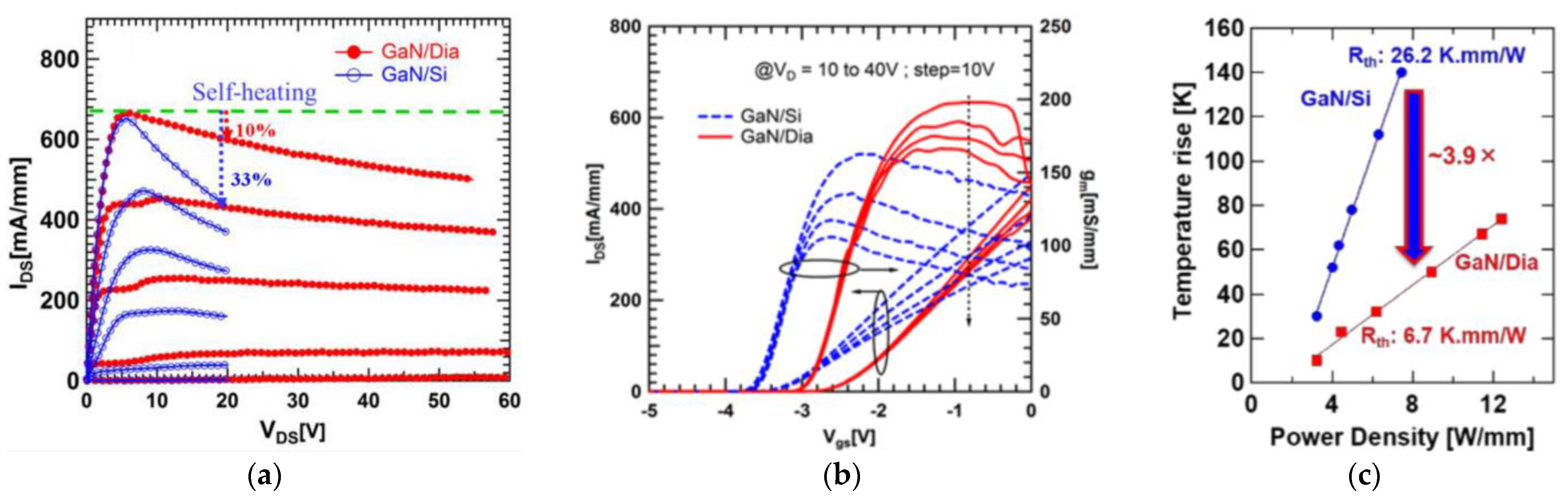
- Due to the intrinsic nature of GaN HEMTs, harsh and localized self-heating in the conducting channel may occur [26]; this effect increases with the device power density and further compromises reliability [22,27]. On one side, the electrical behavior of the traps mentioned in the above paragraph is temperature-dependent [25]. On the other side, additional phonon scattering in the channel degrades the 2DEG effective carrier mobility, leading to degraded DC and RF performance [28]. Finally, since the relation between the mean time-to-failure (MTTF) of an electronic component and its operating temperature is semi-exponential [29], even a small temperature reduction can have a great impact on the lifetime of HEMTs with thermally-activated degradation mechanisms [30].
2. Thermal Management of GaN HEMTs
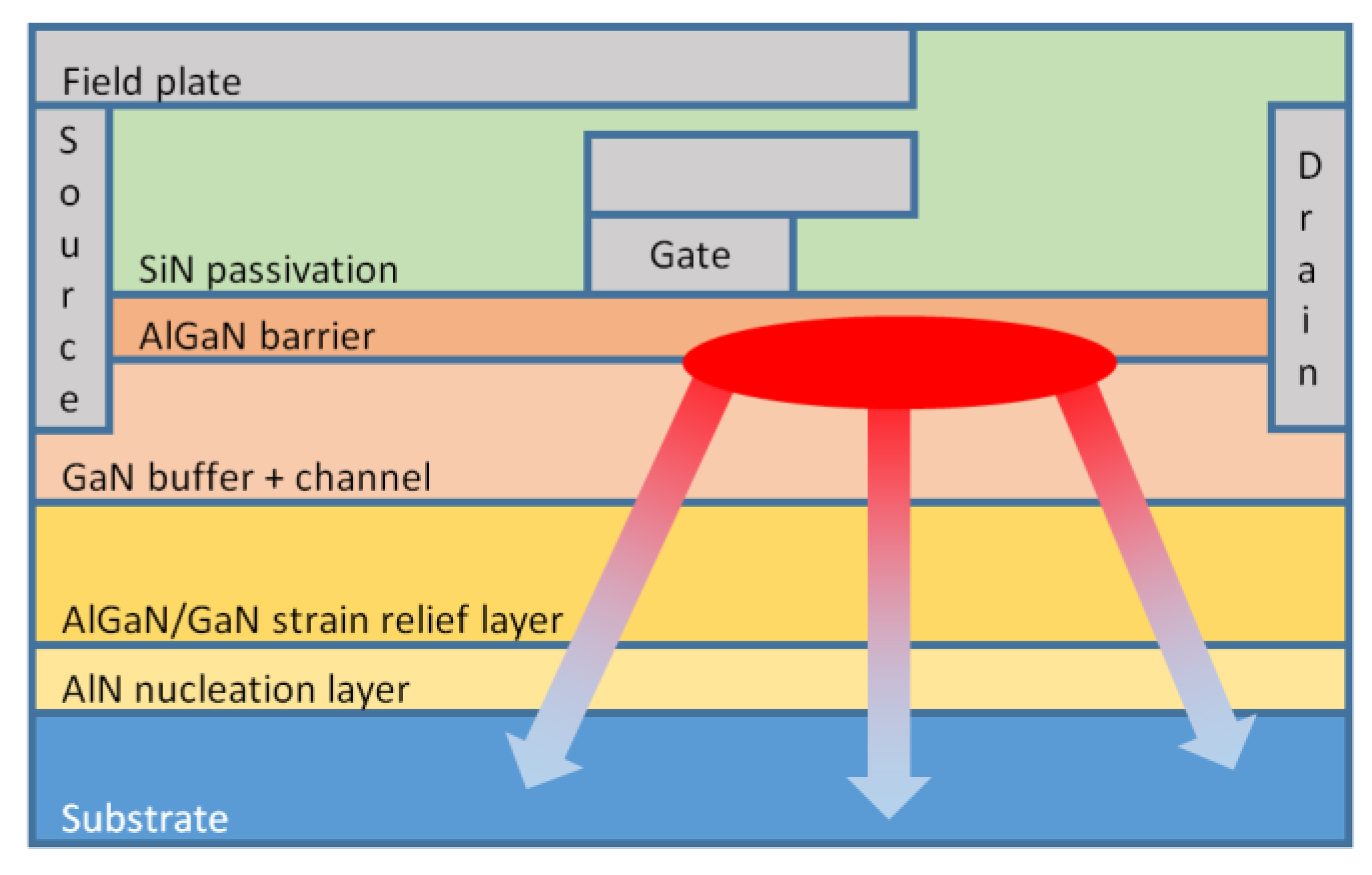
2.1. GaN HEMT
- Substrate. Homoepitaxial growth of GaN-based films is hampered by the limited availability of GaN substrates in standard wafer sizes. As a consequence, the different layers are typically deposited by either Molecular Beam Epitaxy (MBE) or MOCVD onto sapphire, Si, or silicon carbide (SiC) substrates. Epitaxial films with dislocation densities of 108 cm−2 are typically obtained [36]; dislocation densities lower than 107 cm−2 involve hydride vapor phase epitaxy (HVPE) growth.
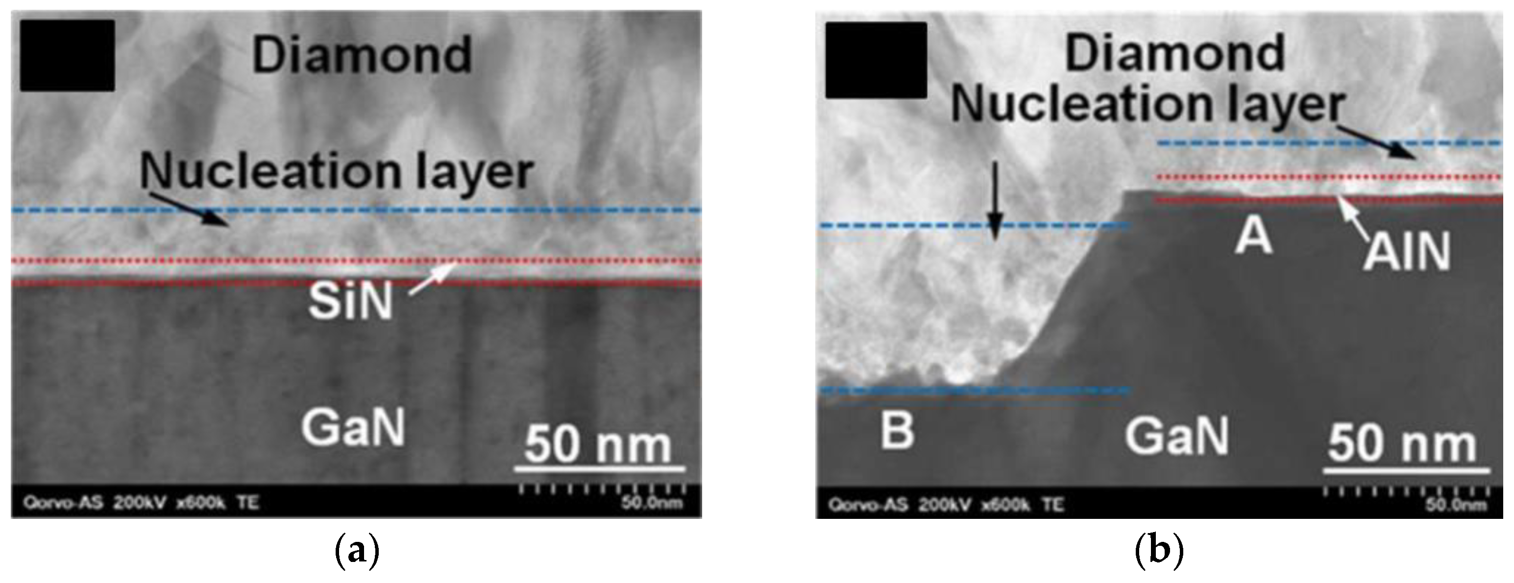
- Nucleation layer. The deposition of high quality epitaxial GaN films with smooth surfaces and low dislocation density is not a straightforward task due to lattice mismatch and to the difference in the coefficients of thermal expansion (CTEs) of GaN and substrate [37]. A nucleation layer, typically 40–200 nm of aluminum nitride (AlN) [38], is thus initially deposited on the substrate surface for strain accommodation and increased interface resistivity [39,40].
- Strain relief layer. AlGaN/GaN transition layers, often up to 1 µm thickness, further accommodate the lattice mismatch during the growth of GaN on the foreign substrate [41].
- GaN layer. A 0.6–1.5 µm-thick GaN buffer layer that provides electrical isolation to reduce substrate leakage and prevents the propagation of threading dislocations and contaminants that might migrate from the substrate into the top high quality channel region follows.
- Passivation layer. A thin dielectric layer, typically silicon nitride (Si3N4), compensates the surface/interface states responsible for the current collapse issue by introducing shallow donors [44].
- Field plate. The source and gate-connected field plates are usually employed to reduce the strength of the electric field near the gate terminal, reducing the gate tunneling injection current responsible for charging the surface traps [45].
2.2. Getting the Heat Out
2.3. Why GaN-Diamond HEMTs?
3. Integration of Diamond and GaN
3.1. GaN-on-Diamond
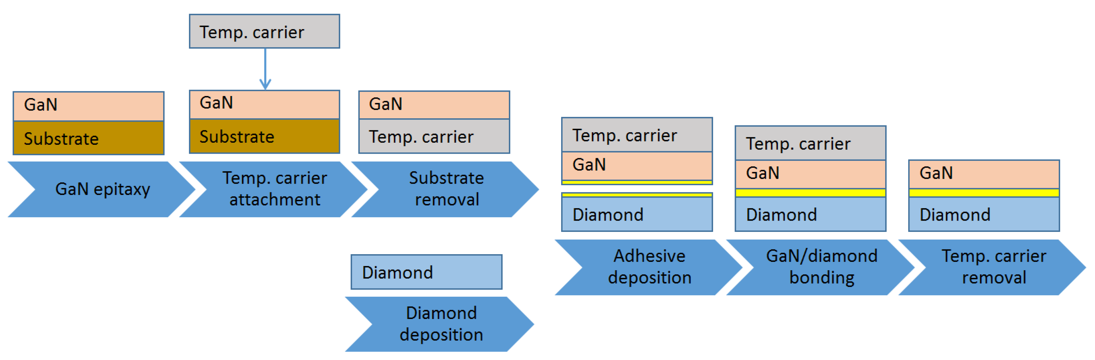
3.2. Bonded Wafers
3.3. GaN Epitaxy
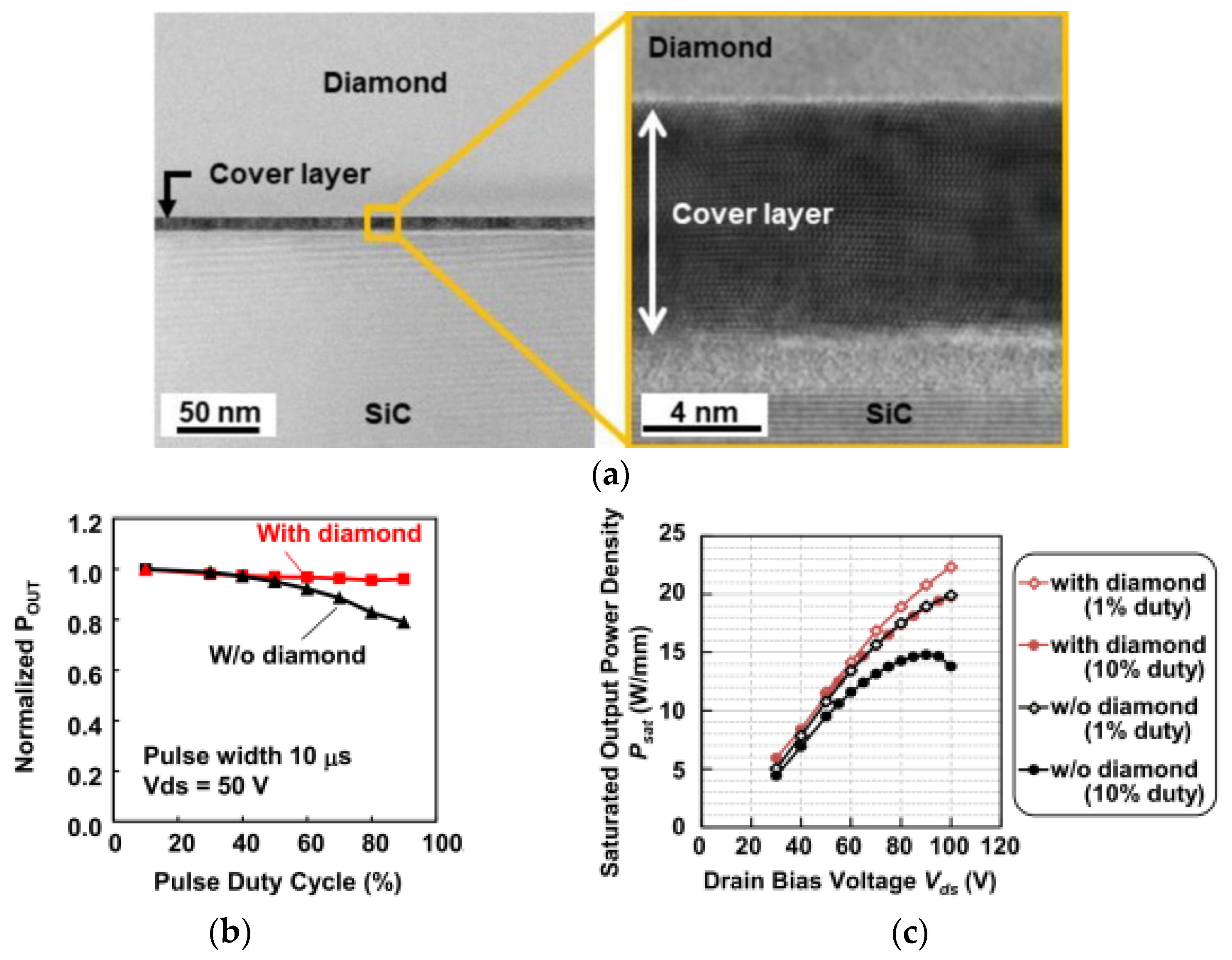
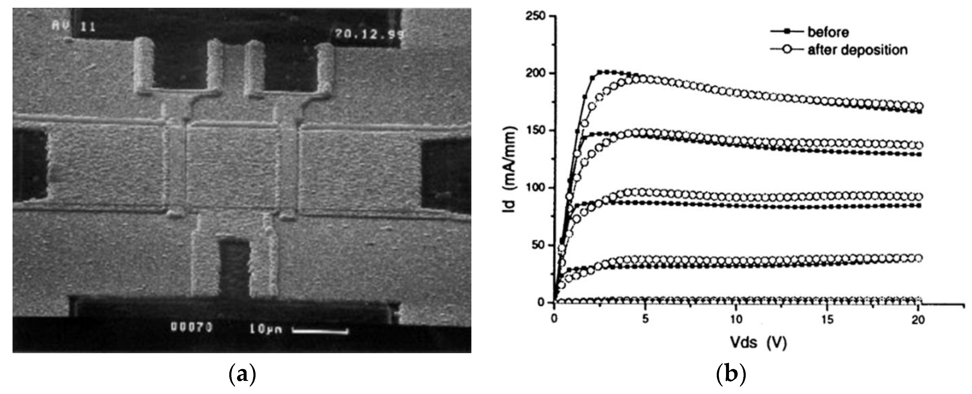
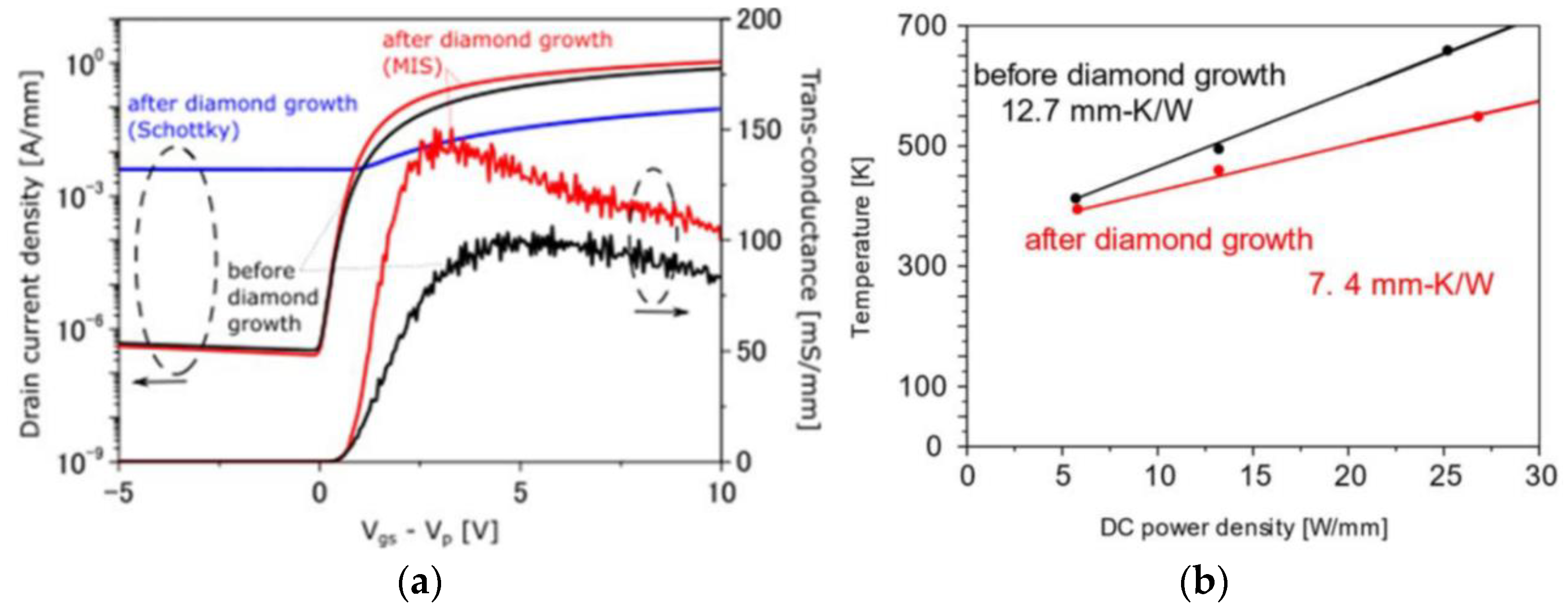
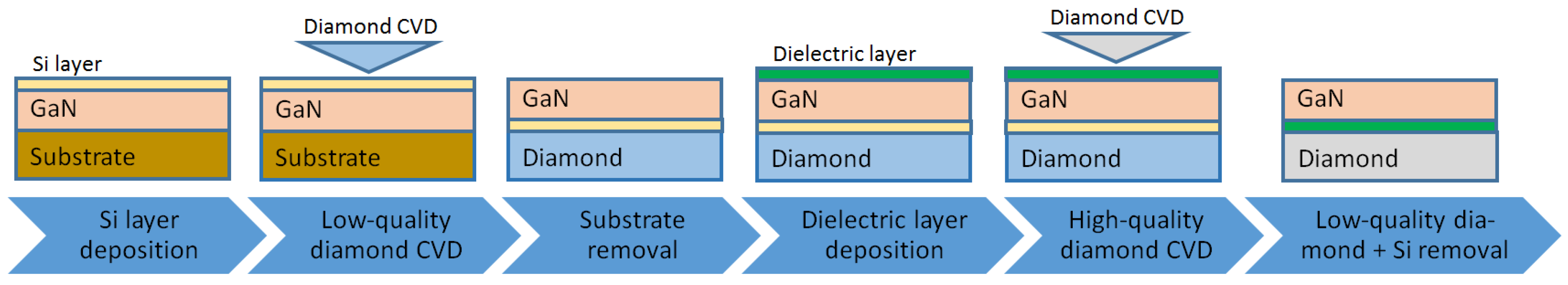
3.4. Capping Diamond
4. GaN/Diamond HEMTs: Where to Go?
4.1. Challenges of Fabricating GaN-on-Diamond Wafers
4.1.1. Decreasing Thermal Stress
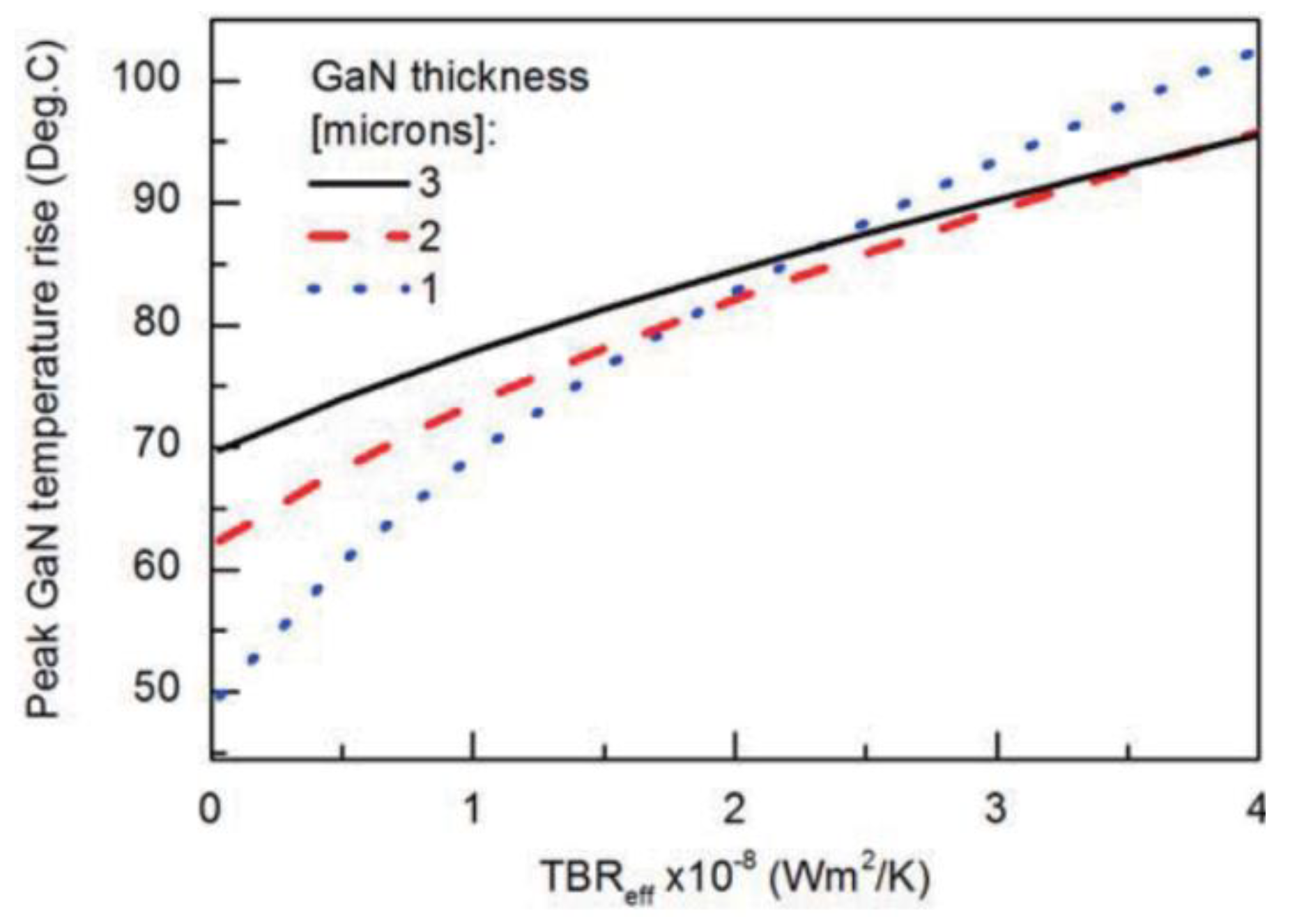
4.1.2. Optimizing the Thermal Barrier Resistance at the Diamond/GaN Interface
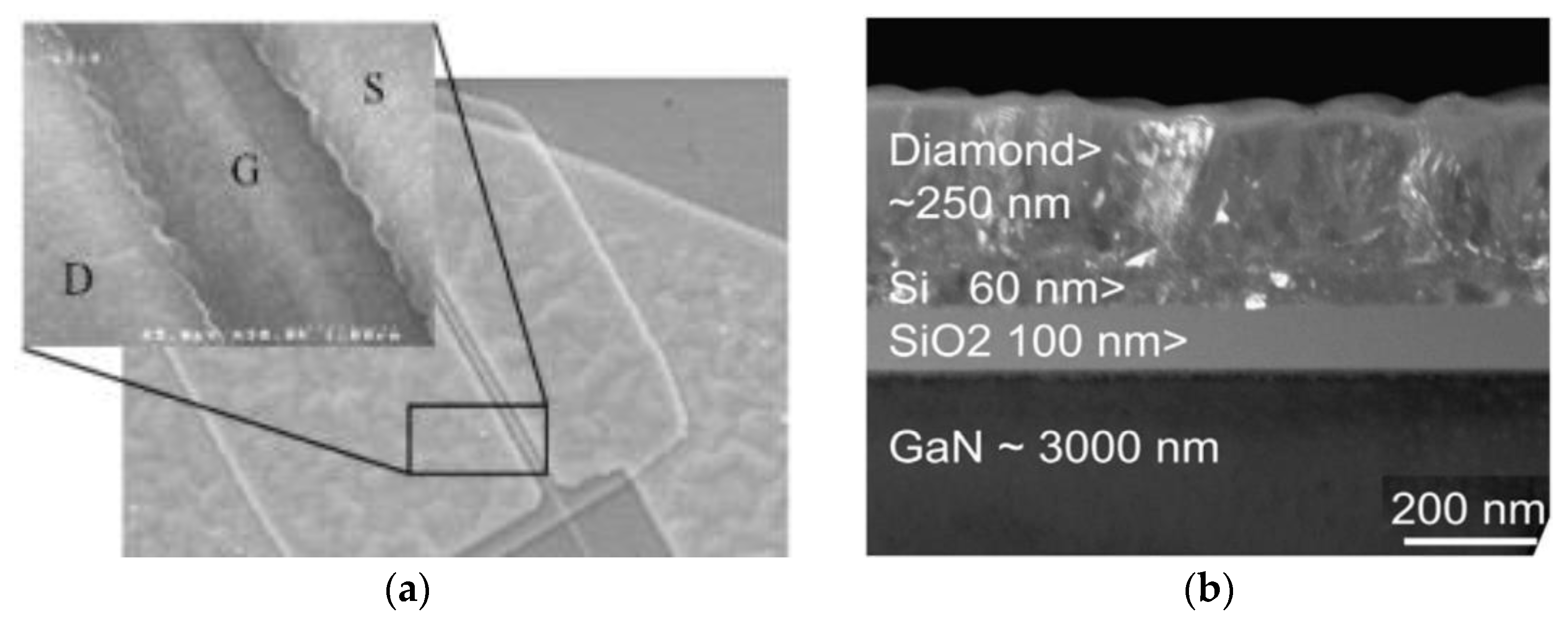
4.1.3. Optimizing Diamond CVD for Thermal Management Applications
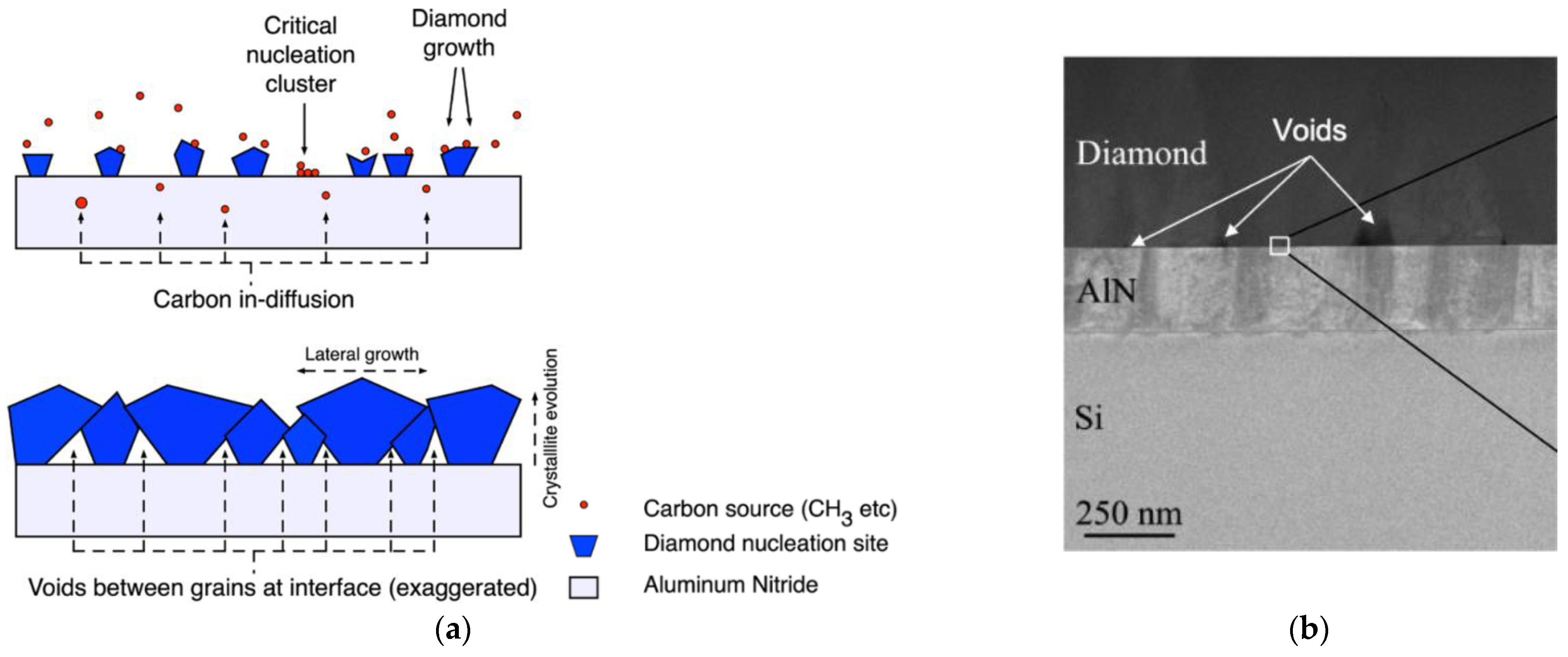
4.1.3.1. Impact of the Seeding Procedure
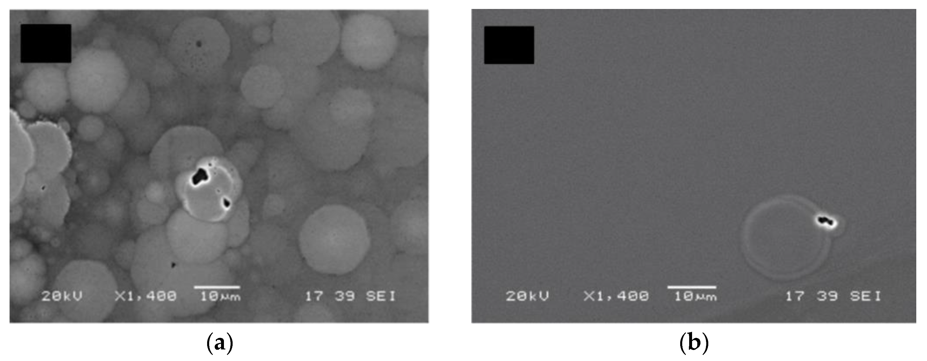
- Ultrasonic agitation in a suspension containing DND seeds. Ultrasonic seeding has been widely used since the early 1990s [176]. Seeding can be performed with different sized diamond grit, as well as with a mixture of diamond grit and metal particles. As an example, the adhesion of 0.25 µm tungsten (W) and Ti particles to a nanodiamond suspension was reported to increase the seeding density and the adhesion of diamond films deposited on Si and Si3N4 substrates [177]. A significant improvement was achieved with DND particles colloidal solutions, which enabled seeding densities in excess of 1012 cm−2 [178].
- Enhancement of electrostatic attraction between DND seeds and substrate. By properly tuning the ζ-potentials of seeds and/or substrates, one can benefit from enhanced electrostatic attraction between the DND seeds and the substrate. This can be achieved by terminating the DND seeds with oxygen (O) or H atoms [179] or by preparing polymer/nanodiamond colloids [180,181]. This effect can be further enhanced by exposing the substrate to a plasma treatment in order to guarantee that the ζ-potentials of diamond seeds and substrate have opposite signs [84].
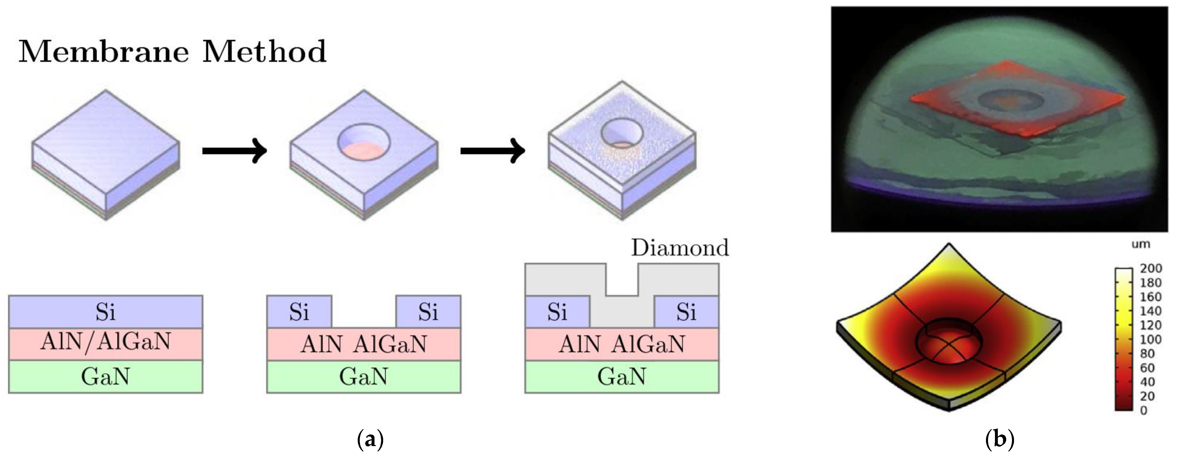
4.1.4. Optimizing the Thickness of the GaN Epilayers
4.2. Challenges of Bonding GaN and Diamond Wafers
4.3. Challenges of Epitaxially Growing GaN on Diamond
4.4. Challenges of Capping GaN HEMTs with Diamond
4.5. What Is the Best Approach?
5. Conclusions
Author Contributions
Funding
Institutional Review Board Statement
Informed Consent Statement
Data Availability Statement
Conflicts of Interest
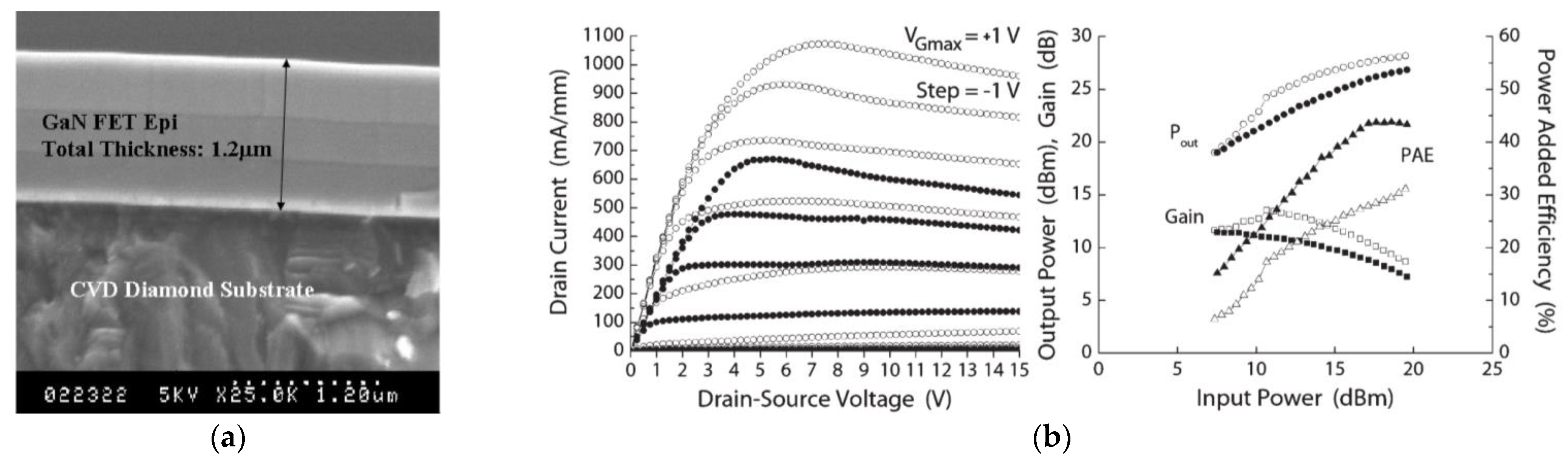
Appendix A. Performance of Diamond/GaN HEMT Transistors

| Ref. | Year | HEMT Dimensions a | DC Measurements | Small-Signal | Large Signal | Rth (K⋅mm/W) | |||||||
|---|---|---|---|---|---|---|---|---|---|---|---|---|---|
| ID max (mA/mm) | gm peak (mS/mm) | PD, DC (W/mm) | VD (V) | fT (GHz) | fmax (GHz) | Conditions | PAE (%) | PD (W/mm) | |||||
| [63] | 2006 | NF/WG/LSD/LG | 2/150/4.5/1.5 | 306 | 70 | -- | -- | 8 | 11.46 | -- | -- | -- | -- |
| [64] | 2007 | NF/WG/LSD/LG | 1/50/4.5/1.2 | 800 | 180 | -- | -- | -- | -- | -- | -- | -- | -- |
| NF/WG/LSD/LG | 2/37.5/4.5/1.2 | -- | -- | -- | 10 | 12.3 | 21.8 | -- | -- | -- | -- | ||
| [65] | 2007 | NF/WG/LSD/LG | 2/125/5.3/0.25 | 670 | 187 | -- | -- | 27.4 | -- | Class B; VD = 25 V | 47 | 2.79 | 6 |
| Class B; VD = 20 V | 44 | 1.92 | -- | ||||||||||
| [66] | 2009 | NF/WG/LGD/LSG/ LG | 2/50/2.5/0.5/ 0.04 | 580 | 220 | -- | -- | 85 | 91 | -- | -- | -- | -- |
| [70,186] | 2013 | NF/WG/LSD/LG | 1/50/4/0.25 | 1100 | 300 | -- | -- | -- | -- | -- | -- | -- | -- |
| NF/WG/LSD/LG | 2/100/4/0.25 | -- | -- | -- | 30 | 30 | -- | 10 GHz; VD = 40 V | >46 | >7 | -- | ||
| [28] | 2019 | NF/WG/LGD/LSG/LG | 2/100/3/2/2 | 662 | 199 | 27.56 | 10 | 10.2 | 31.4 | -- | -- | -- | 6.7 |
| [101] | 2019 | -- | -- | -- | -- | 56 | -- | -- | -- | -- | -- | -- | 2.95 |
| [102] | 2019 | NF/WG/LG | 2/300/0.5 | -- | -- | -- | -- | -- | -- | Pulsed; PW = 50 µs; DC = 10%; VD = 100 V | -- | 22.5 | -- |
| NF/WG/LG | 10/50/0.5 | -- | -- | -- | -- | -- | -- | Pulsed; PW = 50 µs; DC = 10%; VD = 100 V | -- | 23.2 | -- | ||
| NF/WG/LG | 10/200/0.5 b | -- | -- | -- | -- | -- | Pulsed; PW = 50 µs; DC = 10%; VD = 80 V | -- | 18.1 | -- | |||
| Ref. | Year | HEMT Dimensions a | DC Measurements | Small-Signal | Large Signal | ||||||
|---|---|---|---|---|---|---|---|---|---|---|---|
| ID max (mA/mm) | gm peak (mS/mm) | VD (V) | fT (GHz) | fmax (GHz) | Conditions | PAE (%) | PD (W/mm) | ||||
| [109] | 2014 | NF/WG | 2/100 | 1000 | 330 | -- | -- | -- | 10 GHz; VD = 20 V; tuned for PD | 38 | 3.4 |
| 10 GHz; VD = 20 V; tuned for PAE | 42 | 3.0 | |||||||||
| 10 GHz; VD = 40 V; tuned for PD | 30 | 6.0 | |||||||||
| 10 GHz; VD = 40 V; tuned for PAE | 33 | 5.4 | |||||||||
| [111] | 2016 | NF/WG | 12/50 | 1200 | 390 | -- | -- | -- | 10 GHz; VD = 40 V | 51 | 11.0 |
| [112] | 2017 | NF/WG | 10/125 | 1000 | -- | -- | -- | -- | -- | -- | -- |
| NF/WG | 4/125 | Class AB; 10 GHz; VD = 28 V | 50.5 | 5.5 | |||||||
| [114] | 2019 | NF/WG | 4 × 8/180 | 640 | -- | -- | -- | -- | -- | -- | -- |
| [118] | 2020 | WG/Pg | 1000/30 | -- | -- | -- | -- | -- | Pulsed; PW = 10 µs; DC = 10%; VD = 50 V | -- | 19.8 |
| Pulsed; PW = 10 µs; DC = 1%; VD = 50 V | 22.3 | ||||||||||
| [119,120] | 2020 | NF/WG/LG | 2/75/0.08 | 690 | 325 | 4 | 85 | 106 | -- | -- | -- |
| [122] | 2018 | NF/WG/LG | 2/300/0.5 | -- | -- | -- | -- | -- | 3 GHz; VD = 50 V; tuned for PD | 46.5 | 6.63 |
| 3 GHz; VD = 50 V; tuned for PAE | 54.2 | 5.39 | |||||||||
| Pulsed; VD = 50 V; tuned for PD | 53.5 | 7.44 | |||||||||
| Pulsed; VDS = 50 V; tuned for PAE | 59.1 | 5.91 | |||||||||
| Ref. | Year | HEMT Dimensions a | DC Measurements | Small-Signal | Large Signal | Rth (K⋅mm/W) | ||||||
|---|---|---|---|---|---|---|---|---|---|---|---|---|
| ID max (mA/mm) | gm peak (mS/mm) | VD (V) | fT (GHz) | fmax (GHz) | Conditions | PAE (%) | PD (W/mm) | |||||
| [129] | 2010 | NF/WG/LG/LSD | 1/50/0.2/4.5 | 730 | 137.5 | 10 | 21 | 42.5 | -- | -- | -- | -- |
| [130] | 2011 | NF/WG/LG/LSD | 1/100/3/20 | 220 | -- | 10 | 3 | 7 | -- | -- | -- | -- |
| NF/WG/LG | 1/630/6 | -- | -- | -- | -- | -- | -- | -- | -- | 4.1 | ||
| [131] | 2012 | NF/WG/LGD/LSG/LG/LSD | 2/100/2.3/2.3/0.4/5 | 770 | 160 | 15 | 25 | 18 | -- | -- | -- | -- |
| NF/WG/LGD/LSG/LG/LSD | 2/400/2.3/2.3/0.4/5 | -- | -- | -- | -- | -- | 1 GHz; VD = 50 V | 46 | 2.13 | 1.5 | ||
| [132] | 2012 | NF/WG/LGD/LSG/LG/LSD | 1/100/7.5/7.5/5/20 | 275 | 60 | -- | -- | -- | -- | -- | -- | -- |
| [133] | 2012 | NF/LG/LGD/LSG/LSD | 1/0.4/2.3/2.3/5 | 800 | 160 | -- | -- | -- | -- | -- | -- | -- |
| Ref. | Year | HEMT Dimensions a | DC Measurements | Small-Signal | Rth (K⋅mm/W) | |||
|---|---|---|---|---|---|---|---|---|
| ID max (mA/mm) | gm peak (mS/mm) | fT (GHz) | fmax (GHz) | |||||
| [46] | 2001 | NF | 2 | 190 | 100 | -- | -- | -- |
| [141] | 2010 | -- | -- | 150 | 113.9 | -- | -- | -- |
| [142] | 2012 | -- | -- | 270 | -- | -- | -- | -- |
| [143,144] | 2013, 2014 | -- | -- | 445 | 127 | -- | -- | 0.96 |
| [145] | 2013 | NF/WG/LG/LSD | 1/100/3/20 | 430 | -- | -- | -- | -- |
| [148] | 2011 | NF/WG/LG | 1/50/0.25 | 400 | 170 | 4.2 | 5 | -- |
| [154] | 2021 | -- | -- | 1100 | 148 | -- | -- | 7.4 |
References
- Roccaforte, F.; Fiorenza, P.; Nigro, R.L.; Giannazzo, F.; Greco, G. Physics and technology of gallium nitride materials for power electronics. Riv. del Nuovo Cim. 2018, 41, 625–681. [Google Scholar]
- Longobardi, G. GaN for power devices: Benefits, applications, and normally-off technologies. Proc. Int. Semicond. Conf. CAS 2017, 2017-Octob, 11–18. [Google Scholar]
- Kuball, M. GaN-on-Diamond Technology Recent UK Successes. In Proceedings of the Diamond D-Day—Workshop hosted by the Centre for Device Thermography and Reliability of the University of Bristol and the GaNDaME Programme, Bristol, UK, 29 January 2019. [Google Scholar]
- Amano, H.; Baines, Y.; Beam, E.; Borga, M.; Bouchet, T.; Chalker, P.R.; Charles, M.; Chen, K.J.; Chowdhury, N.; Chu, R.; et al. The 2018 GaN power electronics roadmap. J. Phys. D Appl. Phys. 2018, 51, 163001. [Google Scholar] [CrossRef]
- Lin, Y.Q.; Patterson, A. Design Solutions for 5G Power Amplifiers using 0.15 μm and 0.25 μm GaN HEMTs. In Proceedings of the 2020 International Symposium on VLSI Design, Automation and Test (VLSI-DAT), Hsinchu, Taiwan, 10–13 August 2020; pp. 31–33. [Google Scholar]
- Iucolano, F.; Boles, T. GaN-on-Si HEMTs for wireless base stations. Mater. Sci. Semicond. Process 2019, 98, 100–105. [Google Scholar] [CrossRef]
- Chow, T.P.; Omura, I.; Higashiwaki, M.; Kawarada, H.; Pala, V. Smart power devices and ICs using GaAs and wide and extreme bandgap semiconductors. IEEE Trans. Electron Devices 2017, 64, 856–873. [Google Scholar] [CrossRef]
- Millán, J. Wide band-gap power semiconductor devices. IET Circ. Devices Syst. 2007, 1, 372–379. [Google Scholar] [CrossRef]
- Gracio, J.J.; Fan, Q.H.; Madaleno, J.C. Diamond growth by chemical vapour deposition. J. Phys. D Appl. Phys. 2010, 43, 374017. [Google Scholar] [CrossRef]
- Yates, L.; Anderson, J.; Gu, X.; Lee, C.; Bai, T.; Mecklenburg, M.; Aoki, T.; Goorsky, M.S.; Kuball, M.; Piner, E.L.; et al. Low Thermal Boundary Resistance Interfaces for GaN-on-Diamond Devices. ACS Appl. Mater. Interfaces 2018, 10, 24302–24309. [Google Scholar] [CrossRef]
- Diamond Materials, The CVD Diamond Booklet. Available online: https://www.diamond-materials.com/site/assets/files/1095/cvd_diamond_booklet.pdf (accessed on 7 October 2021).
- Watanabe, H.; Yamada, N.; Okaji, M. Linear thermal expansion coefficient of silicon from 293 to 1000 K. Int. J. Thermophys. 2004, 25, 221–236. [Google Scholar] [CrossRef]
- Stockmeier, M.; Müller, R.; Sakwe, S.A.; Wellmann, P.J.; Magerl, A. On the lattice parameters of silicon carbide. J. Appl. Phys. 2009, 105, 033511. [Google Scholar] [CrossRef]
- He, J.; Cheng, W.C.; Wang, Q.; Cheng, K.; Yu, H.; Chai, Y. Recent Advances in GaN-Based Power HEMT Devices. Adv. Electron. Mater. 2021, 7, 2001045. [Google Scholar] [CrossRef]
- Palacios, T.; Suh, C.-S.; Chakraborty, A.; Keller, S.; DenBaars, S.P.; Mishra, U.K. High-Performance E-Mode AlGaN/GaN HEMTs. IEEE Electron Device Lett. 2006, 27, 428–430. [Google Scholar] [CrossRef]
- Lu, B.; Saadat, O.I.; Palacios, T. High-Performance Integrated Dual-Gate AlGaN/GaN Enhancement-Mode Transistor. IEEE Electron Device Lett. 2010, 31, 990–992. [Google Scholar] [CrossRef]
- Longobardi, G.; Udrea, F.; Sque, S.; Croon, J.; Hurkx, F.; Šonskỳ, J. Investigation of surface charges and traps in gallium nitride/aluminium gallium nitride/gallium nitride high-voltage transistors via measurements and technology computer-aided design simulations of transfer characteristics of metal-insulator-semiconductor. IET Power Electron. 2015, 8, 2322–2328. [Google Scholar] [CrossRef]
- Hu, J.; Stoffels, S.; Lenci, S.; Groeseneken, G.; Decoutere, S. On the identification of buffer trapping for bias-dependent dynamic RON of AlGaN/GaN schottky barrier diode with AlGaN:C back barrier. IEEE Electron Device Lett. 2016, 37, 310–313. [Google Scholar] [CrossRef]
- Mizutani, T.; Ohno, Y.; Akita, M.; Kishimoto, S.; Maezawa, K. A study on current collapse in AlGaN/GaN HEMTs induced by bias stress. IEEE Trans. Electron Devices 2003, 50, 2015–2020. [Google Scholar] [CrossRef]
- Meneghesso, G.; Meneghini, M.; Zanoni, E. Reliability and instabilities in GaN-based HEMTs. In Proceedings of the 2014 IEEE International Conference on Electron Devices and Solid-State Circuits, EDSSC 2014, Chengdu, China, 18–20 June 2014; pp. 5–6. [Google Scholar]
- Wang, M.; Yan, D.; Zhang, C.; Xie, B.; Wen, C.P.; Wang, J.; Hao, Y.; Wu, W.; Shen, B. Investigation of surface- and buffer-induced current collapse in GaN high-electron mobility transistors using a soft switched pulsed I-V measurement. IEEE Electron Device Lett. 2014, 35, 1094–1096. [Google Scholar] [CrossRef]
- Jin, D.; del Alamo, J.A. Mechanisms responsible for dynamic ON-resistance in GaN high-voltage HEMTs. In Proceedings of the 2012 24th International Symposium on Power Semiconductor Devices and ICs, Bruges, Belgium, 3–7 June 2012; pp. 333–336. [Google Scholar]
- Ubochi, B.; Faramehr, S.; Ahmeda, K.; Igić, P.; Kalna, K. Operational frequency degradation induced trapping in scaled GaN HEMTs. Microelectron. Reliab. 2017, 71, 35–40. [Google Scholar] [CrossRef]
- McGovern, P.; Tasker, P.J.; Powell, J.R.; Hilton, K.P.; Glasper, J.L.; Balmer, R.S.; Martin, T.; Uren, M.J. Analysis of DC-RF Dispersion in AlGaN/GaN HFETs Using Pulsed I-V and Time-Domain Waveform Measurements. In Proceedings of the IEEE MTT-S International Microwave Symposium Digest, Long Beach, CA, USA, 17 June 2005; pp. 513–516. [Google Scholar]
- Gomes, J.L.; Nunes, L.C.; Goncalves, C.F.; Pedro, J.C. An Accurate Characterization of Capture Time Constants in GaN HEMTs. IEEE Trans. Microw. Theory Technol. 2019, 67, 2465–2474. [Google Scholar] [CrossRef]
- Gaska, R.; Osinsky, A.; Yang, J.W.; Shur, M.S. Self-heating in high-power AlGaN-GaN HFETs. IEEE Electron Device Lett. 1998, 19, 89–91. [Google Scholar] [CrossRef]
- Azarifar, M.; Donmezer, N. A multiscale analytical correction technique for two-dimensional thermal models of AlGaN/GaN HEMTs. Microelectron. Reliab. 2017, 74, 82–87. [Google Scholar] [CrossRef]
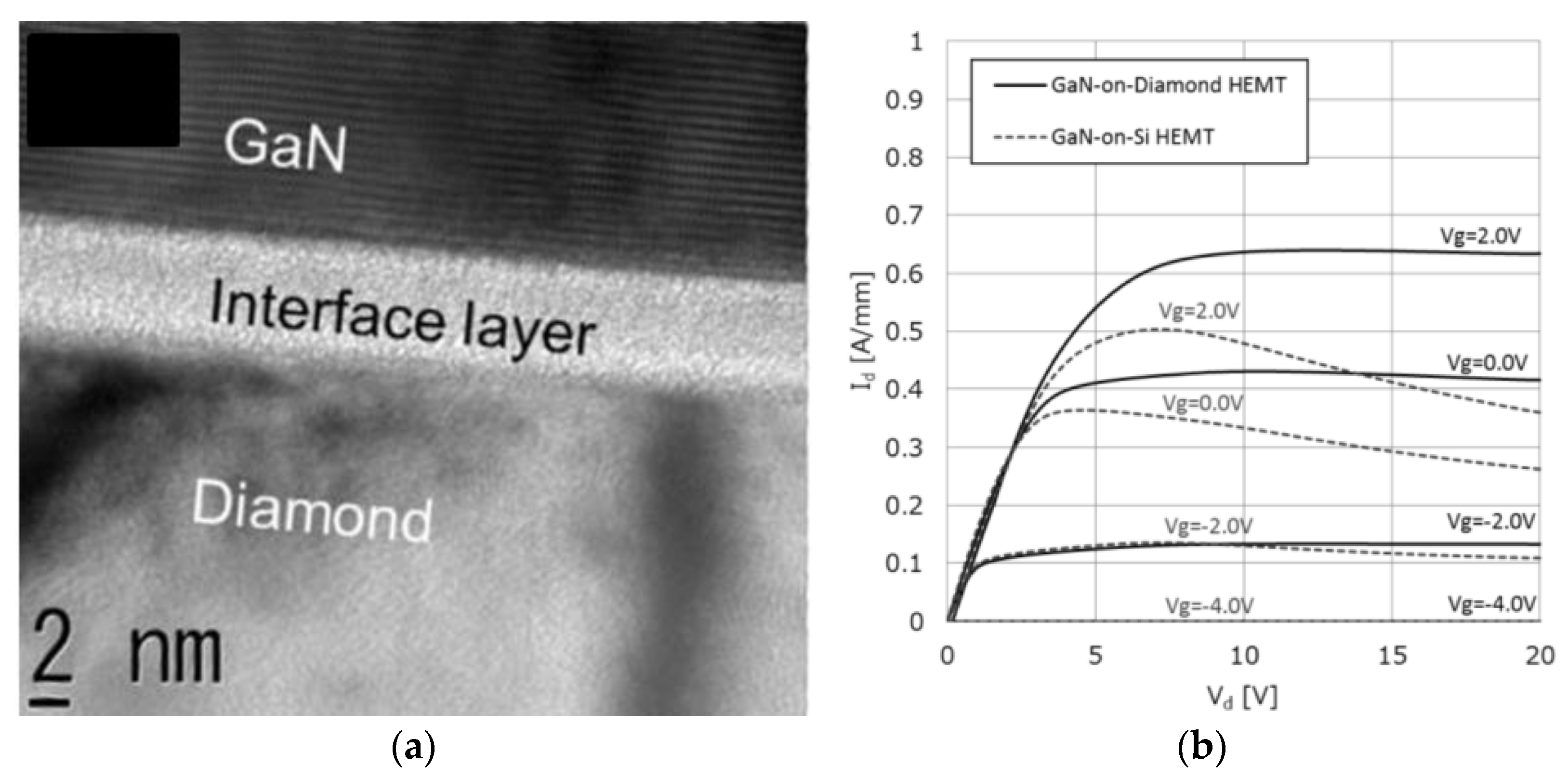
- Ranjan, K.; Arulkumaran, S.; Ng, G.I.; Sandupatla, A. Investigation of Self-Heating Effect on DC and RF Performances in AlGaN/GaN HEMTs on CVD-Diamond. IEEE J. Electron Devices Soc. 2019, 7, 1264–1269. [Google Scholar] [CrossRef]
- Kraus, A.D.; Bar-cohen, A. Thermal Analysis and Control of Electronic Equipment; Hemisphere Pub. Corp.: Washington, DC, USA, 1983. [Google Scholar]
- Joshin, K.; Kikkawa, T. High-power and high-efficiency GaN HEMT amplifiers. In Proceedings of the 2008 IEEE Radio and Wireless Symposium, Orlando, FL, USA, 22–24 January 2008; pp. 65–68. [Google Scholar]
- Darwish, A.M.; Bayba, A.J.; Hung, H.A. Thermal resistance calculation of AlGaN-GaN devices. IEEE Trans. Microw. Theory Technol. 2004, 52, 2611–2620. [Google Scholar] [CrossRef]
- Dingle, R.; Störmer, H.L.; Gossard, A.C.; Wiegmann, W. Electron mobilities in modulation-doped semiconductor heterojunction superlattices. Appl. Phys. Lett. 1978, 33, 665–667. [Google Scholar] [CrossRef]
- Mimura, T.; Hiyamizu, S.; Fujii, T.; Nanbu, K. A New Field-Effect Transistor with Selectively Doped {GaAs}/n-{AlxGa}1-{xAs} Heterojunctions. Jpn. J. Appl. Phys. 1980, 19, L225–L227. [Google Scholar] [CrossRef]
- Nakamura, S.; Harada, Y.; Seno, M. Novel metalorganic chemical vapor deposition system for GaN growth. Appl. Phys. Lett. 1991, 58, 2021–2023. [Google Scholar] [CrossRef]
- Khan, M.A.; Bhattarai, A.; Kuznia, J.N.; Olson, D.T. High electron mobility transistor based on a GaN-AlxGa 1-xN heterojunction. Appl. Phys. Lett. 1993, 63, 1214–1215. [Google Scholar] [CrossRef]
- Keller, S. Substrates and Materials. In Power GaN Devices: Materials, Applications and Reliability; Meneghini, M., Meneghesso, G., Zanoni, E., Eds.; Springer International Publishing: Cham, Switzerland, 2017; pp. 27–52. [Google Scholar]
- Amano, H.; Sawaki, N.; Akasaki, I.; Toyoda, Y. Metalorganic vapor phase epitaxial growth of a high quality GaN film using an AlN buffer layer. Appl. Phys. Lett. 1986, 48, 353–355. [Google Scholar] [CrossRef] [Green Version]
- Manoi, A.; Pomeroy, J.W.; Killat, N.; Kuball, M. Benchmarking of thermal boundary resistance in AlGaN/GaN HEMTs on SiC substrates: Implications of the nucleation layer microstructure. IEEE Electron Device Lett. 2010, 31, 1395–1397. [Google Scholar] [CrossRef]
- Chang, S.; Zhao, M.; Spampinato, V.; Franquet, A.; Chang, L. The influence of AlN nucleation layer on RF transmission loss of GaN buffer on high resistivity Si (111) substrate. Semicond. Sci. Technol. 2020, 35, 035029. [Google Scholar] [CrossRef]
- Chen, J.-T.; Pomeroy, J.W.; Rorsman, N.; Xia, C.; Virojanadara, C.; Forsberg, U.; Kuball, M.; Janzén, E. Low thermal resistance of a GaN-on-SiC transistor structure with improved structural properties at the interface. J. Cryst. Growth 2015, 428, 54–58. [Google Scholar] [CrossRef] [Green Version]
- Pomeroy, J.; Bernardoni, M.; Sarua, A.; Manoi, A.; Dumka, D.C.; Fanning, D.M.; Kuball, M. Achieving the best thermal performance for GaN-on-diamond. In Proceeding of the IEEE Compound Semiconductor Integrated Circuit Symposium, CSICS, Monterey, CA, USA, 13–16 October 2013; pp. 1–4. [Google Scholar]
- Smorchkova, I.P.; Chen, L.; Mates, T.; Shen, L.; Heikman, S.; Moran, B.; Keller, S.; DenBaars, S.P.; Speck, J.S.; Mishra, U.K. AlN/GaN and (Al,Ga)N/AlN/GaN two-dimensional electron gas structures grown by plasma-assisted molecular-beam epitaxy. J. Appl. Phys. 2001, 90, 5196–5201. [Google Scholar] [CrossRef]
- Lee, D.S.; Gao, X.; Guo, S.; Kopp, D.; Fay, P.; Palacios, T. 300-GHz InAlN/GaN HEMTs With InGaN Back Barrier. IEEE Electron Device Lett. 2011, 32, 1525–1527. [Google Scholar] [CrossRef]
- Yang, S.; Tang, Z.; Hua, M.; Zhang, Z.; Wei, J.; Lu, Y.; Chen, K.J. Investigation of SiNx and AlN Passivation for AlGaN/GaN High-Electron-Mobility Transistors: Role of Interface Traps and Polarization Charges. IEEE J. Electron Devices Soc. 2020, 8, 358–364. [Google Scholar] [CrossRef]
- Brannick, A.; Zakhleniuk, N.A.; Ridley, B.K.; Shealy, J.R.; Schaff, W.J.; Eastman, L.F. Influence of Field Plate on the Transient Operation of the AlGaN/GaN HEMT. IEEE Electron Device Lett. 2009, 30, 436–438. [Google Scholar] [CrossRef]
- Seelmann-Eggebert, M.; Meisen, P.; Schaudel, F.; Koidl, P.; Vescan, A.; Leier, H. Heat-spreading diamond films for GaN-based high-power transistor devices. Diam. Relat. Mater. 2001, 10, 744–749. [Google Scholar] [CrossRef]
- Mitterhuber, L.; Hammer, R.; Dengg, T.; Spitaler, J. Thermal Characterization and Modelling of AlGaN-GaN Multilayer Structures for HEMT Applications. Energies 2020, 13, 2363. [Google Scholar] [CrossRef]
- Kucukgok, B.; Wu, X.; Wang, X.; Liu, Z.; Ferguson, I.T.; Lu, N. The structural properties of InGaN alloys and the interdependence on the thermoelectric behavior. AIP Adv. 2016, 6, 25305. [Google Scholar] [CrossRef] [Green Version]
- Ejeckam, F.; Francis, D.; Faili, F.; Twitchen, D.; Bolliger, B.; Babic, D.; Felbinger, J. S2-T1: GaN-on-diamond: A brief history. In Proceedings of the Lester Eastman Conference 2014—High Perform. Devices, LEC, Ithaca, NY, USA, 5–7 August 2014; pp. 1–5. [Google Scholar]
- Swartz, E.T.; Pohl, R.O. Thermal boundary resistance. Rev. Mod. Phys. 1989, 61, 605–668. [Google Scholar] [CrossRef]
- Bao, W.; Wang, Z.; Tang, D. Phonon transport across GaN/AlN interface: Interfacial phonon modes and phonon local non-equilibrium analysis. Int. J. Heat Mass Transf. 2022, 183, 122090. [Google Scholar] [CrossRef]
- Zhao, Y.; Zhu, C.; Wang, S.; Tian, J.Z.; Yang, D.J.; Chen, C.K.; Cheng, H.; Hing, P. Pulsed photothermal reflectance measurement of the thermal conductivity of sputtered aluminum nitride thin films. J. Appl. Phys. 2004, 96, 4563–4568. [Google Scholar] [CrossRef]
- Zou, J.; Kotchetkov, D.; Balandin, A.A.; Florescu, D.I.; Pollak, F.H. Thermal conductivity of GaN films: Effects of impurities and dislocations. J. Appl. Phys. 2002, 92, 2534–2539. [Google Scholar] [CrossRef]
- Riedel, G.J.; Pomeroy, J.W.; Hilton, K.P.; Maclean, J.O.; Wallis, D.J.; Uren, M.J.; Martin, T.; Forsberg, U.; Lundskog, A.; Kakanakova-Georgieva, A.; et al. Reducing thermal resistance of AlGaN/GaN electronic devices using novel nucleation layers. IEEE Electron Device Lett. 2009, 30, 103–106. [Google Scholar] [CrossRef]
- Sarua, A.; Ji, H.; Hilton, K.P.; Wallis, D.J.; Uren, M.J.; Martin, T.; Kuball, M. Thermal boundary resistance between GaN and substrate in AlGaN/GaN electronic devices. IEEE Trans. Electron Devices 2007, 54, 3152–3158. [Google Scholar] [CrossRef]
- Inagaki, M.; Kaburagi, Y.; Hishiyama, Y. Thermal management material: Graphite. Adv. Eng. Mater. 2014, 16, 494–506. [Google Scholar] [CrossRef]
- Chu, R.C.; Ellsworth, J.M.J.; Marotta, E.; Singh, P. Graphite-Based Heat Sinks and Apparatus for the Manufacture Thereof. U.S. Patent 6,907,917 B2, 21 June 2005. [Google Scholar]
- Huang, Y.; Ouyang, Q.; Guo, Q.; Guo, X.; Zhang, G.; Zhang, D. Graphite film/aluminum laminate composites with ultrahigh thermal conductivity for thermal management applications. Mater. Des. 2016, 90, 508–515. [Google Scholar] [CrossRef]
- Balandin, A.A. Thermal properties of graphene and nanostructured carbon materials. Nat. Mater. 2011, 10, 569–581. [Google Scholar] [CrossRef] [PubMed] [Green Version]
- Huang, P.; Li, Y.; Yang, G.; Li, Z.-X.; Li, Y.-Q.; Hu, N.; Fu, S.-Y.; Novoselov, K.S. Graphene film for thermal management: A review. Nano Mater. Sci. 2021, 3, 1–16. [Google Scholar] [CrossRef]
- Yan, Z.; Liu, G.; Khan, J.M.; Balandin, A.A. Graphene quilts for thermal management of high-power GaN transistors. Nat. Commun. 2012, 3, 827–828. [Google Scholar] [CrossRef] [PubMed]
- Mukherjee, D.; Mendes, J.C.; Alves, L.N. Diamond for Future (Power) Electronics. Power Electron. Eur. 2020, 4, 6–8. [Google Scholar]
- Jessen, G.H.; Gillespie, J.K.; Via, G.D.; Crespo, A.; Langley, D.; Wasserbauer, J.; Faili, F.; Francis, D.; Babic, D.; Ejeckam, F.; et al. AlGaN/GaN HEMT on diamond technology demonstration. In Proceedings of the Technical Digest—IEEE Compound Semiconductor Integrated Circuit Symposium, CSIC, San Antonio, TX, USA, 12–15 November 2006; pp. 271–274. [Google Scholar]
- Dumka, D.C.; Saunier, P. AlGaN/GaN HEMTs on diamond substrate. In Proceedings of the 65th DRC Device Research Conference, South Bend, Indiana, 18–20 June 2007; pp. 31–32. [Google Scholar]
- Felbinger, J.G.; Chandra, M.V.S.; Sun, Y.; Eastman, L.F.; Wasserbauer, J.; Faili, F.; Babic, D.; Francis, D.; Ejeckam, F. Comparison of GaN HEMTs on diamond and SiC substrates. IEEE Electron Device Lett. 2007, 28, 948–950. [Google Scholar] [CrossRef]
- Diduck, Q.; Felbinger, J.; Eastman, L.F.; Francis, D.; Wasserbauer, J.; Faili, F.; Babić, D.I.; Ejeckam, F. Frequency performance enhancement of AlGaN/GaN HEMTs on diamond. Electron. Lett. 2009, 45, 758–759. [Google Scholar] [CrossRef]
- Babić, D.I.; Diduck, Q.; Yenigalla, P.; Schreiber, A.; Francis, D.; Faili, F.; Ejeckam, F.; Felbinger, J.G.; Eastman, L.F. GaN-on-diamond field-effect transistors: From wafers to amplifier modules. In Proceedings of the International Convention on Information and Communications Technology, Electronics and Microelectronics (MIPRO), Opatija, Hrvatska, 24–28 May 2010; pp. 60–66. [Google Scholar]
- Dumka, D.C.; Chowdhury, U.; Jimenez, J.L.; Chou, T.-M.; Ketterson, A.; Fanning, D.M.; Murdock, B.; Faili, F.; Francis, D.; Ejeckam, F. Near-Junction Thermal Management in High Power GaN HEMTs. In Proceedings of the Government Microcircuit Applications and Critical Technology Conf. (GOMACTech 2012), Las Vegas, NV, USA, 19–22 March 2012; Volume 556, pp. 6–9. [Google Scholar]
- Cho, J.; Li, Z.; Bozorg-Grayeli, E.; Kodama, T.; Francis, D.; Ejeckam, F.; Faili, F.; Asheghi, M.; Goodson, K.E. Improved thermal interfaces of GaN-Diamond composite substrates for HEMT applications. IEEE Trans. Compon. Packag. Manuf. Technol. 2013, 3, 79–85. [Google Scholar] [CrossRef]
- Dumka, D.C.; Chou, T.M.; Jimenez, J.L.; Fanning, D.M.; Francis, D.; Faili, F.; Ejeckam, F.; Bernardoni, M.; Pomeroy, J.W.; Kuball, M. Electrical and thermal performance of AlGaN/GaN HEMTs on diamond substrate for RF applications. In Proceedings of the 2013 IEEE Compound Semiconductor Integrated Circuit Symposium (CSICS), Monterey, CA, USA, 13–16 October 2013; pp. 1–4. [Google Scholar]
- Altman, D.; Tyhach, M.; McClymonds, J.; Kim, S.; Graham, S.; Cho, J.; Goodson, K.; Francis, D.; Faili, F.; Ejeckam, F.; et al. Analysis and characterization of thermal transport in GaN HEMTs on Diamond substrates. In Proceedings of the Intersociety Conference on Thermal and Thermomechanical Phenomena in Electronic Systems (ITherm), Orlando, FL, USA, 27–30 May 2014; pp. 1199–1205. [Google Scholar]
- Pomeroy, J.W.; Bernardoni, M.; Dumka, D.C.; Fanning, D.M.; Kuball, M. Low thermal resistance GaN-on-diamond transistors characterized by three-dimensional Raman thermography mapping. Appl. Phys. Lett. 2014, 104, 083513. [Google Scholar] [CrossRef] [Green Version]
- el Helou, A.; Tadjer, M.; Hobart, K.; Raad, P.E. Effects of Thermal Boundary Resistance on the Thermal Performance of GaN HEMT on Diamond. In Proceedings of the 2020 IEEE International Reliability Physics Symposium (IRPS), Dallas, TX, USA, 28 April–30 May 2020; pp. 2–5. [Google Scholar]
- Waller, W.M.; Pomeroy, J.W.; Field, D.; Smith, E.J.W.; May, P.W.; Kuball, M. Thermal boundary resistance of direct van der Waals bonded GaN-on-diamond. Semicond. Sci. Technol. 2020, 35, 095021. [Google Scholar] [CrossRef]
- Wu, Q.; Wu, Q.; Xu, Y.; Zhou, J.; Kong, Y.; Chen, T.; Wang, Y.; Lin, F.; Fu, Y.; Jia, Y.; et al. Performance Comparison of GaN HEMTs on Diamond and SiC Substrates Based on Surface Potential Model. ECS J. Solid State Sci. Technol. 2017, 6, Q171–Q178. [Google Scholar] [CrossRef] [Green Version]
- Smith, E.J.W.; Piracha, A.H.; Field, D.; Pomeroy, J.W.; Mackenzie, G.R.; Abdallah, Z.; Massabuau, F.C.P.; Hinz, A.M.; Wallis, D.J.; Oliver, R.A.; et al. Mixed-size diamond seeding for low-thermal-barrier growth of CVD diamond onto GaN and AlN. Carbon N. Y. 2020, 167, 620–626. [Google Scholar] [CrossRef]
- Pomeroy, J.W.; Simon, R.B.; Sun, H.; Francis, D.; Faili, F.; Twitchen, D.J.; Kuball, M. Contactless thermal boundary resistance measurement of GaN-on-diamond wafers. IEEE Electron Device Lett. 2014, 35, 1007–1009. [Google Scholar] [CrossRef] [Green Version]
- Sun, H.; Simon, R.B.; Pomeroy, J.W.; Francis, D.; Faili, F.; Twitchen, D.J.; Kuball, M. Reducing GaN-on-diamond interfacial thermal resistance for high power transistor applications. Appl. Phys. Lett. 2015, 106, 111906. [Google Scholar] [CrossRef] [Green Version]
- Sun, H.; Pomeroy, J.W.; Simon, R.B.; Francis, D.; Faili, F.; Twitchen, D.J.; Kuball, M. Temperature-Dependent Thermal Resistance of GaN-on-Diamond HEMT Wafers. IEEE Electron Device Lett. 2016, 37, 621–624. [Google Scholar] [CrossRef]
- Cho, J.; Francis, D.; Altman, D.H.; Asheghi, M.; Goodson, K.E. Phonon conduction in GaN-diamond composite substrates. J. Appl. Phys. 2017, 121, 055105. [Google Scholar] [CrossRef]
- Liu, D.; Francis, D.; Faili, F.; Middleton, C.; Anaya, J.; Pomeroy, J.W.; Twitchen, D.J.; Kuball, M. Impact of diamond seeding on the microstructural properties and thermal stability of GaN-on-diamond wafers for high-power electronic devices. Scr. Mater. 2017, 128, 57–60. [Google Scholar] [CrossRef] [Green Version]
- Zhou, Y.; Anaya, J.; Pomeroy, J.; Sun, H.; Gu, X.; Xie, A.; Beam, E.; Becker, M.; Grotjohn, T.A.; Lee, C.; et al. Barrier layer optimization for enhanced GaN-on-diamond device cooling. ACS Appl. Mater. Interfaces 2017, 9, 34416–34422. [Google Scholar] [CrossRef]
- Jia, X.; Wei, J.-J.; Kong, Y.; Li, C.-M.; Liu, J.; Chen, L.; Sun, F.; Wang, X. The influence of dielectric layer on the thermal boundary resistance of GaN-on-diamond substrate. Surf. Interface Anal. 2019, 51, 783–790. [Google Scholar] [CrossRef]
- Mandal, S.; Yuan, C.; Massabuau, F.; Pomeroy, J.W.; Cuenca, J.; Bland, H.; Thomas, E.; Wallis, D.; Batten, T.; Morgan, D.; et al. Thick, Adherent Diamond Films on AlN with Low Thermal Barrier Resistance. ACS Appl. Mater. Interfaces 2019, 11, 40826–40834. [Google Scholar] [CrossRef] [Green Version]
- Park, K.; Bayram, C. Thermal resistance optimization of GaN/substrate stacks considering thermal boundary resistance and temperature-dependent thermal conductivity. Appl. Phys. Lett. 2016, 109, 151904. [Google Scholar] [CrossRef]
- Guo, H.; Kong, Y.; Chen, T. Thermal simulation of high power GaN-on-diamond substrates for HEMT applications. Diam. Relat. Mater. 2017, 73, 260–266. [Google Scholar] [CrossRef]
- Guo, H.; Kong, Y.; Chen, T. Impact of thermal boundary resistance on the thermal design of GaN-on-diamond HEMTs. In Proceedings of the 2019 IEEE 69th Electronic Components and Technology Conference (ECTC), Las Vegas, NV, USA, 28–31 May 2019; Volume 2019-May, pp. 1842–1847. [Google Scholar]
- Middleton, C.; Chandrasekar, H.; Singh, M.; Pomeroy, J.W.; Uren, M.J.; Francis, D.; Kuball, M. Impact of thinning the GaN buffer and interface layer on thermal and electrical performance in GaN-on-diamond electronic devices. Appl. Phys. Express 2019, 12, 024003. [Google Scholar] [CrossRef]
- Zou, B.; Sun, H.; Guo, H.; Dai, B.; Zhu, J. Thermal characteristics of GaN-on-diamond HEMTs: Impact of anisotropic and inhomogeneous thermal conductivity of polycrystalline diamond. Diam. Relat. Mater. 2019, 95, 28–35. [Google Scholar] [CrossRef]
- Song, C.; Kim, J.; Cho, J. The effect of GaN epilayer thickness on the near-junction thermal resistance of GaN-on-diamond devices. Int. J. Heat Mass Transf. 2020, 158, 119992. [Google Scholar] [CrossRef]
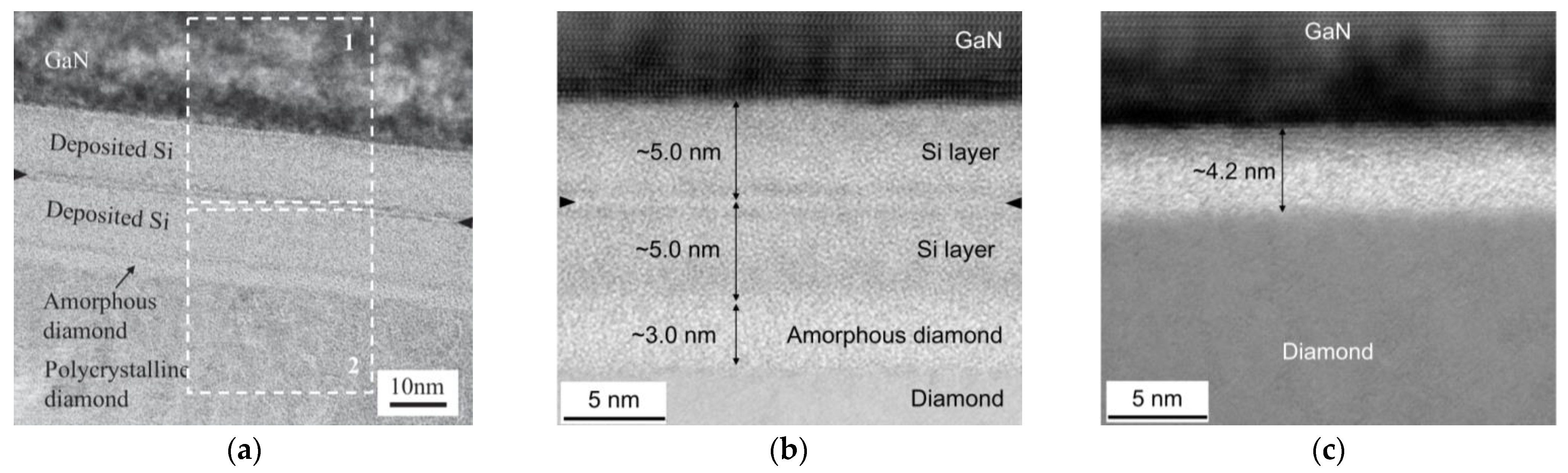
- Siddique, A.; Ahmed, R.; Anderson, J.; Nazari, M.; Yates, L.; Graham, S.; Holtz, M.; Piner, E.L. Structure and Interface Analysis of Diamond on an AlGaN/GaN HEMT Utilizing an in Situ SiNx Interlayer Grown by MOCVD. ACS Appl. Electron. Mater. 2019, 1, 1387–1399. [Google Scholar] [CrossRef]
- Hancock, B.L.; Nazari, M.; Anderson, J.; Piner, E.; Faili, F.; Oh, S.; Twitchen, D.; Graham, S.; Holtz, M. Ultraviolet micro-Raman spectroscopy stress mapping of a 75-mm GaN-on-diamond wafer. Appl. Phys. Lett. 2016, 108, 211901. [Google Scholar] [CrossRef]
- Hines, N.J. Advanced Solutions for Thermal Management and Reliabiliy of Gallium Nitride-Based High Electron Mobility Transistors on Diamond Substrates. Doctoral Thesis, Georgia Institute of Technology, Atlanta, GA, USA, 2019. [Google Scholar]
- Smith, M.D.; Cuenca, J.A.; Field, D.E.; Fu, Y.C.; Yuan, C.; Massabuau, F.; Mandal, S.; Pomeroy, J.W.; Oliver, R.A.; Uren, M.J.; et al. GaN-on-diamond technology platform: Bonding-free membrane manufacturing process. AIP Adv. 2020, 10, 035306. [Google Scholar] [CrossRef]
- Cuenca, J.A.; Smith, M.D.; Field, D.E.; Massabuau, F.C.-P.; Mandal, S.; Pomeroy, J.; Wallis, D.J.; Oliver, R.A.; Thayne, I.; Kuball, M.; et al. Thermal stress modelling of diamond on GaN/III-Nitride membranes. Carbon 2021, 174, 647–661. [Google Scholar] [CrossRef]
- Jia, X.; Wei, J.; Huang, Y.; Shao, S.; An, K.; Kong, Y.; Liu, J.; Chen, L.; Li, C. Fabrication of low stress GaN-on-diamond structure via dual-sided diamond film deposition. J. Mater. Sci. 2021, 56, 6903–6911. [Google Scholar] [CrossRef]
- Liu, D.; Sun, H.; Pomeroy, J.W.; Francis, D.; Faili, F.; Twitchen, D.J.; Kuball, M. GaN-on-diamond electronic device reliability: Mechanical and thermo-mechanical integrity. Appl. Phys. Lett. 2015, 107, 251902. [Google Scholar] [CrossRef] [Green Version]
- Zhai, W.; Zhang, J.; Chen, X.; Bu, R.; Wang, H.; Hou, X. FEM thermal and stress analysis of bonded GaN-on-diamond substrate. AIP Adv. 2017, 7, 095105. [Google Scholar] [CrossRef] [Green Version]
- Liu, D.; Fabes, S.; Li, B.S.; Francis, D.; Ritchie, R.O.; Kuball, M. Characterization of the Interfacial Toughness in a Novel ‘GaN-on-Diamond’ Material for High-Power RF Devices. ACS Appl. Electron. Mater. 2019, 1, 354–369. [Google Scholar] [CrossRef]
- Ranjan, K.; Ing, N.G.; Arulkumaran, S.; Vicknesh, S.; Foo, S.C. Enhanced DC and RF performance of AlGaN/GaN HEMTs on CVD-Diamond in high power CW operation. In Proceedings of the 2019 Electron Devices Technology and Manufacturing Conference (EDTM 2019), Singapore, 12–15 March 2019; pp. 97–99. [Google Scholar]
- Tadjer, M.J.; Anderson, T.J.; Ancona, M.G.; Raad, P.E.; Komarov, P.; Bai, T.; Gallagher, J.C.; Koehler, A.D.; Goorsky, M.S.; Francis, D.A.; et al. GaN-On-Diamond HEMT Technology with TAVG = 176 C at PDC,max = 56 W/mm Measured by Transient Thermoreflectance Imaging. IEEE Electron Device Lett. 2019, 40, 881–884. [Google Scholar] [CrossRef]
- Lee, W.S.; Lee, K.W.; Lee, S.H.; Cho, K.; Cho, S. A GaN/Diamond HEMTs with 23 W/mm for Next Generation High Power RF Application. In Proceedings of the IEEE MTT-S International Microwave Symposium Digest, Boston, MA, USA, 2–7 June 2019; pp. 1395–1398. [Google Scholar]
- Cho, J.; Won, Y.; Francis, D.; Asheghi, M.; Goodson, K.E. Thermal interface resistance measurements for GaN-on-diamond composite substrates. In Proceedings of the 2014 IEEE Compound Semiconductor Integrated Circuit Symposium (CSICS), La Jolla, CA, USA, 19–22 October 2014; pp. 1–4. [Google Scholar]
- Bolliger, B.; Ejeckam, F.; Dodson, J.; Faili, F.; Francis, D.; Lowe, F.; Twitchen, D. CVD diamond for enhanced GaN devices. In Proceedings of the 2014 Asia-Pacific Microwave Conference, Sendai, Japan, 4–7 November 2014. [Google Scholar]
- Tyhach, M.; Altman, D.; Bernstein, S.; Korenstein, R.; Cho, J.; Goodson, K.E.; Francis, D.; Faili, F.; Ejeckam, F.; Kim, S.; et al. S2-T3: Next generation gallium nitride HEMTs enabled by diamond substrates. In Proceedings of the 2014 Lester Eastman Conference on High Performance Devices (LEC), Ithaca, NY, USA, 5–7 August 2014. [Google Scholar]
- Field, D.E.; Cuenca, J.A.; Smith, M.; Fairclough, S.M.; Massabuau, F.C.-P.; Pomeroy, J.W.; Williams, O.; Oliver, R.A.; Thayne, I.; Kuball, M. Crystalline Interlayers for Reducing the Effective Thermal Boundary Resistance in GaN-on-Diamond. ACS Appl. Mater. Interfaces 2020, 12, 54138–54145. [Google Scholar] [CrossRef]
- Chao, P.C.; Chu, K.; Creamer, C. A new high power GaN-on-diamond HEMT with low-temperature bonded substrate technology. In Proceedings of the 2013 International Conference on Compound Semiconductor Manufacturing Technology, CS MANTECH 2013, New Orleans, LA, USA, 13–16 May 2013; pp. 179–182. [Google Scholar]
- Chu, K.K.; Yurovchak, T.; Chao, P.C.; Creamer, C.T. Thermal modeling of high power GaN-on-diamond HEMTs fabricated by low-temperature device transfer process. In Proceedings of the 2013 IEEE Compound Semiconductor Integrated Circuit Symposium (CSICS), Monterey, CA, USA, 13–16 October 2013; pp. 6–9. [Google Scholar]
- Chu, K.K.; Chao, P.C.; Diaz, J.A.; Yurovchak, T.; Creamer, C.T.; Sweetland, S.; Kallaher, R.L.; McGray, C. S2-T4: Low-temperature substrate bonding technology for high power GaN-on-diamond HEMTs. In Proceedings of the 2014 Lester Eastman Conference on High Performance Devices (LEC), Ithaca, NY, USA, 5–7 August 2014; pp. 1–4. [Google Scholar]
- Chao, P.C.; Chu, K.; Diaz, J.; Creamer, C.; Sweetland, S.; Kallaher, R.; McGray, C.; Via, G.D.; Blevins, J. GaN-on-Diamond HEMTs with 11 W/mm Output Power at 10 GHz. MRS Adv. 2016, 1, 147–155. [Google Scholar] [CrossRef]
- Chu, K.K.; Chao, P.C.; Diaz, J.A.; Yurovchak, T.; Schmanski, B.J.; Creamer, C.T.; Sweetland, S.; Kallaher, R.L.; McGray, C.; Via, G.D.; et al. High-Performance GaN-on-Diamond HEMTs Fabricated by Low-Temperature Device Transfer Process. In Proceedings of the 2015 IEEE Compound Semiconductor Integrated Circuit Symposium (CSICS), New Orleans, LA, USA, 11–14 October 2015; pp. 7–10. [Google Scholar]
- Liu, T.; Kong, Y.; Wu, L.; Guo, H.; Zhou, J.; Kong, C.; Chen, T. 3-inch GaN-on-Diamond HEMTs with Device-First Transfer Technology. IEEE Electron Device Lett. 2017, 38, 1417–1420. [Google Scholar] [CrossRef]
- Mu, F.; He, R.; Suga, T. Room temperature GaN-diamond bonding for high-power GaN-on-diamond devices. Scr. Mater. 2018, 150, 148–151. [Google Scholar] [CrossRef]
- Hiza, S.; Fujikawa, M.; Takiguchi, Y.; Nishimura, K.; Yagyu, E.; Matsumae, T.; Kurashima, Y.; Takagi, H.; Yamamuka, M. High-Power GaN-on-Diamond HEMTs Fabricated by Surface-Activated Room-Temperature Bonding. In Proceedings of the 2019 International Conference on Solid State Devices and Materials, Aichi, Japan, 2–5 September 2019; Volume 04, pp. 467–468. [Google Scholar]
- Cheng, Z.; Mu, F.; Yates, L.; Suga, T.; Graham, S. Interfacial Thermal Conductance across Room-Temperature Bonded GaN-Diamond Interfaces for GaN-on-Diamond Devices. ACS Appl. Mater. Interfaces 2020, 12, 8376–8384. [Google Scholar] [CrossRef] [PubMed]
- Suga, T.; Mu, F. Direct Bonding of GaN to Diamond Substrate at Room Temperature. In Proceedings of the 2020 IEEE 70th Electronic Components and Technology Conference (ECTC), Orlando, FL, USA, 3–30 June 2020; pp. 1328–1331. [Google Scholar]
- Wang, K.; Ruan, K.; Hu, W.; Wu, S.; Wang, H. Room temperature bonding of GaN on diamond wafers by using Mo/Au nano-layer for high-power semiconductor devices. Scr. Mater. 2020, 174, 87–90. [Google Scholar] [CrossRef]
- Minoura, Y.; Ohki, T.; Okamoto, N.; Yamada, A.; Makiyama, K.; Kotani, J.; Ozaki, S.; Sato, M.; Nakamura, N. Surface activated bonding of SiC/diamond for thermal management of high-output power GaN HEMTs. Jpn. J. Appl. Phys. 2020, 59, SGGD03. [Google Scholar] [CrossRef]
- Abou Daher, M.; Lesecq, M.; Tilmant, P.; Defrance, N.; Rousseau, M.; Cordier, Y.; De Jaeger, J.C.; Tartarin, J.G. AlGaN/GaN high electron mobility transistors on diamond substrate obtained through aluminum nitride bonding technology. J. Vac. Sci. Technol. B 2020, 38, 033201. [Google Scholar] [CrossRef]
- Abou Daher, M.; Lesecq, M.; Defrance, N.; Okada, E.; Boudart, B.; Guhel, Y.; Tartarin, J.G.; de Jaeger, J.C. Electrical and thermal analysis of AlGaN/GaN HEMTs transferred onto diamond substrate through an aluminum nitride layer. Microw. Opt. Technol. Lett. 2021, 63, 1–5. [Google Scholar] [CrossRef]
- Yablonovitch, E.; Hwang, D.M.; Gmitter, T.J.; Florez, L.T.; Harbison, J.P. Van der Waals bonding of GaAs epitaxial liftoff films onto arbitrary substrates. Appl. Phys. Lett. 1990, 56, 2419–2421. [Google Scholar] [CrossRef]
- Gerrer, T.; Cimalla, V.; Waltereit, P.; Müller, S.; Benkhelifa, F.; Maier, T.; Czap, H.; Ambacher, O.; Quay, R. Transfer of AlGaN/GaN RF-devices onto diamond substrates via van der Waals bonding. Int. J. Microw. Wirel. Technol. 2018, 10, 666–673. [Google Scholar] [CrossRef] [Green Version]
- Cimalla, V. Low Temperature Bonding of GaN electronics on diamond heat spreaders. In Proceedings of the Diamond D-Day—Workshop hosted by the Centre for Device Thermography and Reliability of the University of Bristol and the GaNDaME Programme, Bristol, UK, 29 January 2019. [Google Scholar]
- Webster, R.F.; Cherns, D.; Kuball, M.; Jiang, Q.; Allsopp, D. Electron microscopy of gallium nitride growth on polycrystalline diamond. Semicond. Sci. Technol. 2015, 30, 114007. [Google Scholar] [CrossRef] [Green Version]
- Hageman, P.R.; Schermer, J.J.; Larsen, P.K. GaN growth on single-crystal diamond substrates by metalorganic chemical vapor deposition and hydride vapour deposition. Thin Solid Films 2003, 443, 9–13. [Google Scholar] [CrossRef]
- van Dreumel, G.W.G.; Tinnemans, P.T.; van Den Heuvel, A.A.J.; Bohnen, T.; Buijnsters, J.G.; ter Meulen, J.J.; van Enckevort, W.J.P.; Hageman, P.R.; Vlieg, E. Realising epitaxial growth of GaN on (001) diamond. J. Appl. Phys. 2011, 110, 013503. [Google Scholar] [CrossRef] [Green Version]
- Dussaigne, A.; Malinverni, M.; Martin, D.; Castiglia, A.; Grandjean, N. GaN grown on (111) single crystal diamond substrate by molecular beam epitaxy. J. Cryst. Growth 2009, 311, 4539–4542. [Google Scholar] [CrossRef]
- Dussaigne, A.; Gonschorek, M.; Malinverni, M.; Py, M.A.; Martin, D.; Mouti, A.; Stadelmann, P.; Grandjean, N. High-mobility AlGaN/GaN two-dimensional electron gas heterostructure grown on (111) single crystal diamond substrate. Jpn. J. Appl. Phys. 2010, 49, 061001. [Google Scholar] [CrossRef]
- Alomari, M.; Dussaigne, A.; Martin, D.; Grandjean, N.; Gaquière, C.; Kohn, E. AlGaN/GaN HEMT on (111) single crystalline diamond. Electron. Lett. 2010, 46, 299–301. [Google Scholar] [CrossRef]
- Hirama, K.; Taniyasu, Y.; Kasu, M. AlGaN/GaN high-electron mobility transistors with low thermal resistance grown on single-crystal diamond (111) substrates by metalorganic vapor-phase epitaxy. Appl. Phys. Lett. 2011, 98, 162112. [Google Scholar] [CrossRef]
- Hirama, K.; Kasu, M.; Taniyasu, Y. RF high-power operation of AlGaN/GaN HEMTs epitaxially grown on diamond. IEEE Electron Device Lett. 2012, 33, 513–515. [Google Scholar] [CrossRef]
- Hirama, K.; Kasu, M.; Taniyasu, Y. Growth and device properties of AlGaN/GaN high-electron mobility transistors on a diamond substrate. Jpn. J. Appl. Phys. 2012, 51, 01AG09. [Google Scholar] [CrossRef]
- Hirama, K.; Taniyasu, Y.; Kasu, M. Epitaxial growth of AlGaN/GaN high-electron mobility transistor structure on diamond (111) surface. Jpn. J. Appl. Phys. 2012, 51, 090114. [Google Scholar] [CrossRef] [Green Version]
- van Dreumel, G.W.G.; Buijnsters, J.G.; Bohnen, T.; ter Meulen, J.J.; Hageman, P.R.; van Enckevort, W.J.P.; Vlieg, E. Growth of GaN on nano-crystalline diamond substrates. Diam. Relat. Mater. 2009, 18, 1043–1047. [Google Scholar] [CrossRef]
- Zhang, D.; Bai, Y.Z.; Qin, F.W.; Bian, J.M.; Jia, F.C.; Wu, Z.L.; Zhao, J.J.; Jiang, X. Preparation and characteristics of GaN films on freestanding CVD thick diamond films. Chin. Phys. Lett. 2010, 27, 018102. [Google Scholar]
- Jiang, Q.; Allsopp, D.W.E.; Bowen, C.R. Growth of GaN epitaxial films on polycrystalline diamond by metal-organic vapor phase epitaxy. J. Phys. D Appl. Phys. 2017, 50, 165103. [Google Scholar] [CrossRef]
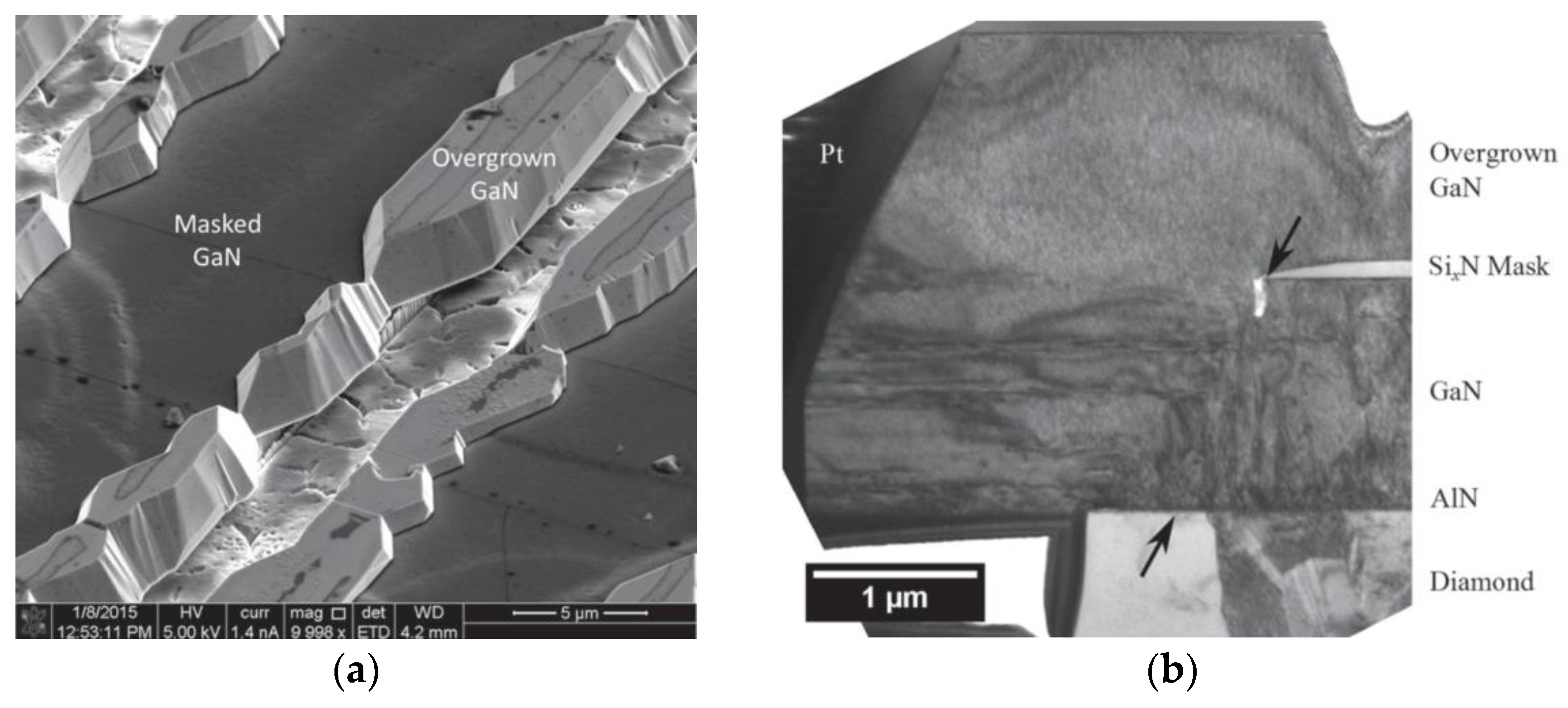
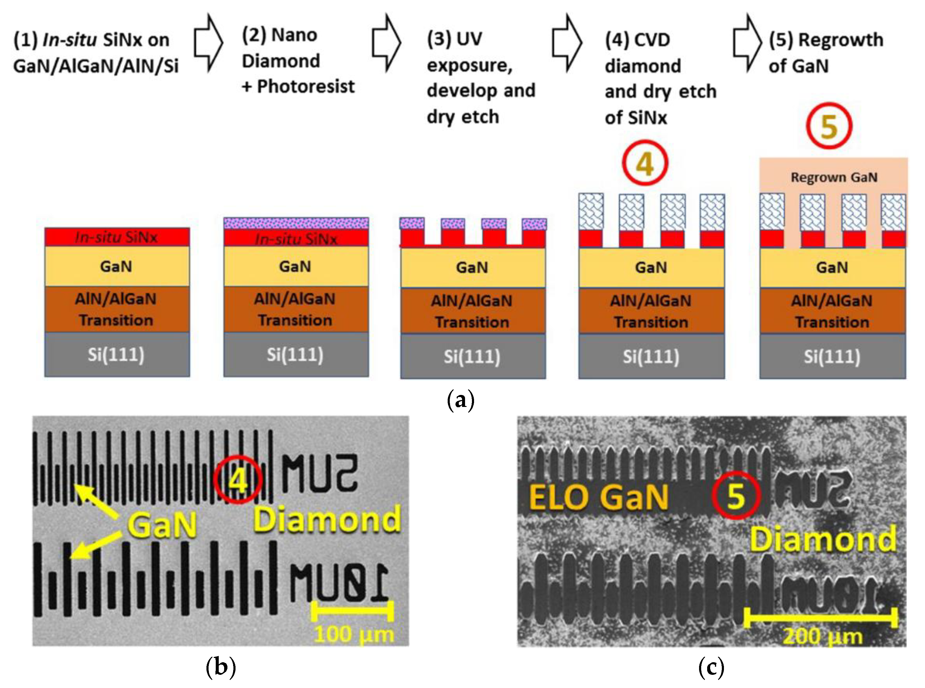
- Ahmed, R.; Siddique, A.; Anderson, J.; Gautam, C.; Holtz, M.; Piner, E. Integration of GaN and Diamond Using Epitaxial Lateral Overgrowth. ACS Appl. Mater. Interfaces 2020, 12, 39397–39404. [Google Scholar] [CrossRef]
- Ahmed, R.; Siddique, A.; Anderson, J.; Engdahl, C.; Holtz, M.; Piner, E. Selective Area Deposition of Hot Filament CVD Diamond on 100 mm MOCVD Grown AlGaN/GaN Wafers. Cryst. Growth Des. 2019, 19, 672–677. [Google Scholar] [CrossRef]
- Rotter, S. Diamond and Diamond-Like-Carbon Films for Electronics. In Workshop on Compound Semiconductor Devices and Integrated Circuits 91 (WOCSDICE 91); Sandia National Labs.: Albuquerque, NM, USA, 1991. [Google Scholar]
- Rotter, S. A proposed novel application of thin overlay diamond films for improved thermal management budget of short gate high power devices. In Proceedings of the Fourth International Conference on New Diamond Science and Technology, Kobe, Japan, 18–22 July 1994; pp. 665–668. [Google Scholar]
- Tadjer, M.J.; Anderson, T.J.; Hobart, K.D.; Feygelson, T.I.; Mastro, M.A.; Caldwell, J.D.; Hite, J.K.; Eddy, C.R., Jr.; Kub, F.J.; Butler, J.E.; et al. Reduced Self-heating in AlGaN/GaN HEMTs Using Nanocrystalline Diamond Heat Spreading Films. In Proceedings of the 68th Device Research Conference, Notre Dame, IN, USA, 21–23 June 2010; pp. 125–126. [Google Scholar]
- Tadjer, M.J.; Anderson, T.J.; Hobart, K.D.; Feygelson, T.I.; Caldwell, J.D.; Eddy, C.R.; Kub, F.J.; Butler, J.E.; Pate, B.; Melngailis, J. Reduced self-heating in AlGaN/GaN HEMTs using nanocrystalline diamond heat-spreading films. IEEE Electron Device Lett. 2012, 33, 23–25. [Google Scholar] [CrossRef]
- Anderson, T.J.; Hobart, K.D.; Tadjer, M.J.; Koehler, A.D.; Feygelson, T.I.; Hite, J.K.; Pate, B.B.; Kub, F.J.; Eddy, C.R., Jr. Nanocrystalline diamond for near junction heat spreading in GaN power HEMTs. In Proceedings of the Technical Digest—IEEE Compound Semiconductor Integrated Circuit Symposium, CSIC, Monterey, CA, USA, 13–16 October 2013; pp. 8–11. [Google Scholar]
- Anderson, T.J.; Hobart, K.D.; Tadjer, M.J.; Koehler, A.D.; Feygelson, T.I.; Pate, B.B.; Hite, J.K.; Kub, F.J.; Eddy, C.R., Jr. Nanocrystalline Diamond for Near Junction Heat Spreading in GaN Power HEMTs. ECS Trans. 2014, 61, 45–49. [Google Scholar] [CrossRef]
- Anderson, T.J.; Koehler, A.D.; Hobart, K.; Tadjer, M.J.; Feygelson, T.I.; Hite, J.K.; Pate, B.B.; Kub, F.J.; Eddy, C.R., Jr. Nanocrystalline Diamond-Gated AlGaN/GaN HEMT. IEEE Electron Device Lett. 2013, 34, 1382–1384. [Google Scholar] [CrossRef]
- Anderson, T.J.; Hobart, K.D.; Tadjer, M.J.; Koehler, A.D.; Imhoff, E.A.; Hite, J.K.; Feygelson, T.I.; Pate, B.B.; Eddy, C.R., Jr.; Kub, F.J. Nanocrystalline Diamond Integration with III-Nitride HEMTs. ECS J. Solid State Sci. Technol. 2017, 6, Q3036–Q3039. [Google Scholar] [CrossRef]
- El Helou, A.; Komarov, P.; Tadjer, M.J.; Anderson, T.J.; Francis, D.A.; Feygelson, T.; Pate, B.B.; Hobart, K.D.; Raad, P.E. High-Resolution Thermoreflectance Imaging Investigation of Self-Heating in AlGaN/GaN HEMTs on Si, SiC, and Diamond Substrates. IEEE Trans. Electron Devices 2020, 67, 5415–5420. [Google Scholar] [CrossRef]
- Alomari, M.; Dipalo, M.; Rossi, S.; Diforte-Poisson, M.A.; Delage, S.; Carlin, J.F.; Grandjean, N.; Gaquiere, C.; Toth, L.; Pecz, B.; et al. Diamond overgrown InAlN/GaN HEMT. Diam. Relat. Mater. 2011, 20, 604–608. [Google Scholar] [CrossRef]
- Kohn, E.; Alomari, M.; Gao, Z.; Rossi, S.; Dussaigne, A.; Carlin, J.-F.; Grandjean, N.; Aretouli, K.; Adikimenakis, A.; Konstantinidis, G.; et al. Direct Integration of Diamond Heat Spreader with GaN-Based HEMT Device Structures. In Proceedings of the High Performance Devices. Lester Eastman Conference (LEC), Ithaca, NY, USA, 5–7 August 2014; pp. 1–4. [Google Scholar]
- Zhou, Y.; Ramaneti, R.; Anaya, J.; Korneychuk, S.; Derluyn, J.; Sun, H.; Pomeroy, J.; Verbeeck, J.; Haenen, K.; Kuball, M. Thermal characterization of polycrystalline diamond thin film heat spreaders grown on GaN HEMTs. Appl. Phys. Lett. 2017, 111, 041901. [Google Scholar] [CrossRef] [Green Version]
- Wang, A.; Tadjer, M.J.; Anderson, T.J.; Baranyai, R.; Pomeroy, J.W.; Feygelson, T.I.; Hobart, K.D.; Pate, B.B.; Calle, F.; Kuball, M. Impact of intrinsic stress in diamond capping layers on the electrical behavior of AlGaN/GaN HEMTs. IEEE Trans. Electron Devices 2013, 60, 3149–3156. [Google Scholar] [CrossRef]
- Soleimanzadeh, R.; Khadar, R.A.; Naamoun, M.; Van Erp, R.; Matioli, E. Near-junction heat spreaders for hot spot thermal management of high power density electronic devices. J. Appl. Phys. 2019, 126, 165113. [Google Scholar] [CrossRef]
- Arivazhagan, L.; Jarndal, A.; Nirmal, D. GaN HEMT on Si substrate with diamond heat spreader for high power applications. J. Comput. Electron. 2021, 20, 873–882. [Google Scholar] [CrossRef]
- Yaita, J.; Yamada, A.; Kotani, J. Growth of microcrystalline diamond films after fabrication of GaN high-electron-mobility transistors for effective heat dissipation. Jpn. J. Appl. Phys. 2021, 60, 076502. [Google Scholar] [CrossRef]
- Fujitsu. Fujitsu Successfully Grows Diamond Film to Boost Heat Dissipation Efficiency of GaN HEMT. Press Release 2019. Available online: https://www.fujitsu.com/global/about/resources/news/press-releases/2019/1205-01.html%202019 (accessed on 7 October 2021).
- Zhang, H.; Guo, Z.; Lu, Y. Enhancement of Hot Spot Cooling by Capped Diamond Layer Deposition for Multifinger AlGaN/GaN HEMTs. IEEE Trans. Electron Devices 2020, 67, 47–52. [Google Scholar] [CrossRef]
- Zhu, T.; Zheng, X.-F.; Cao, Y.-R.; Wang, C.; Mao, W.; Wang, Y.-Z.; Mi, M.-H.; Wu, M.; Mo, J.-H.; Ma, X.-H.; et al. Study on the Effect of Diamond Layer on the Performance of Double-Channel AlGaN/GaN HEMTs. Semicond. Sci. Technol. 2020, 35, 055006. [Google Scholar] [CrossRef]
- Zhang, H.; Guo, Z. Thickness Dependence and Anisotropy of Capped Diamond Thermal Conductivity on Cooling of Pulse-Operated GaN HEMTs. IEEE Trans. Compon. Packag. Manuf. Technol. 2021, 11, 233–240. [Google Scholar] [CrossRef]
- Moelle, C.; Klose, S.; Szücs, F.; Fecht, H.J.; Johnston, C.; Chalker, P.R.; Werner, M. Measurement and calculation of the thermal expansion coefficient of diamond. Diam. Relat. Mater. 1997, 6, 839–842. [Google Scholar] [CrossRef]
- Reeber, R.R.; Wang, K. Lattice parameters and thermal expansion of GaN. J. Mater. Res. 2000, 15, 40–44. [Google Scholar] [CrossRef]
- Tripathy, S.; Chua, S.J.; Chen, P.; Miao, Z.L. Micro-Raman investigation of strain in GaN and AlxGa 1-xN/GaN heterostructures grown on Si(111). J. Appl. Phys. 2002, 92, 3503. [Google Scholar] [CrossRef]
- Ahmad, I.; Holtz, M.; Faleev, N.N.; Temkin, H. Dependence of the stress-temperature coefficient on dislocation density in epitaxial GaN grown on α-Al2O3 and 6H-SiC substrates. J. Appl. Phys. 2004, 95, 1692–1697. [Google Scholar] [CrossRef] [Green Version]
- Choi, S.; Heller, E.; Dorsey, D.; Vetury, R.; Graham, S. The impact of mechanical stress on the degradation of AlGaN/GaN high electron mobility transistors. J. Appl. Phys. 2013, 114, 164501. [Google Scholar] [CrossRef]
- Kang, B.S.; Kim, S.; Kim, J.; Ren, F. Effect of external strain on the conductivity of AlGaN/GaN high-electron-mobility transistors. Appl. Phys. Lett. 2003, 83, 4845. [Google Scholar] [CrossRef]
- Slack, G.A.; Tanzilli, R.A.; Pohl, R.O.; Vandersande, J.W. The intrinsic thermal conductivity of AIN. J. Phys. Chem. Solids 1987, 48, 641–647. [Google Scholar] [CrossRef]
- Pobedinskas, P.; Degutis, G.; Dexters, W.; Hardy, A.; van Bael, M.K.; Haenen, K. Influence of hydrogen and hydrogen/methane plasmas on AlN thin films. Appl. Phys. Lett. 2014, 104, 081917. [Google Scholar] [CrossRef]
- Pobedinskas, P.; Degutis, G.; Dexters, W.; Janssen, W.; Janssens, S.D.; Conings, B.; Ruttens, B.; D’Haen, J.; Boyen, H.-G.; Hardy, A.; et al. Surface plasma pretreatment for enhanced diamond nucleation on AlN. Appl. Phys. Lett. 2013, 102, 201609. [Google Scholar] [CrossRef] [Green Version]
- Smith, M.D.; Li, X.; Uren, M.J.; Thayne, I.G.; Kuball, M. Polarity dependence in Cl2-based plasma etching of GaN, AlGaN and AlN. Appl. Surf. Sci. 2020, 521, 146297. [Google Scholar] [CrossRef]
- Song, C.; Kim, J.; Lee, H.; Cho, J. Fundamental limits for near-junction conduction cooling of high power GaN-on-diamond devices. Solid State Commun. 2019, 295, 12–15. [Google Scholar] [CrossRef]
- van der Drift, A. Evolutionary selection, a principle governing growth orientation in vapour-deposited layers. Philips Res. Rep. 1967, 22, 267–288. [Google Scholar]
- Ophus, C.; Ewalds, T.; Luber, E.J.; Mitlin, D. The role of self-shadowing on growth and scaling laws of faceted polycrystalline thin films. Acta Mater. 2010, 58, 5150–5159. [Google Scholar] [CrossRef]
- Smereka, P.; Li, X.; Russo, G.; Srolovitz, D.J. Simulation of faceted film growth in three dimensions: Microstructure, morphology and texture. Acta Mater. 2005, 53, 1191–1204. [Google Scholar] [CrossRef]
- Liu, T.; Raabe, D.; Mao, W.-M. A review of crystallographic textures in chemical vapor-deposited diamond films. Front. Mater. Sci. China 2010, 4, 1–16. [Google Scholar] [CrossRef]
- Graebner, J.E.; Jin, S.; Kammlott, G.W.; Bacon, B.; Seibles, L.; Banholzer, W. Anisotropic thermal conductivity in chemical vapor deposition diamond. J. Appl. Phys. 1992, 71, 5353–5356. [Google Scholar] [CrossRef]
- Anaya, J.; Sun, H.; Pomeroy, J.; Kuball, M. Thermal management of GaN-on-diamond high electron mobility transistors: Effect of the nanostructure in the diamond near nucleation region. In Proceedings of the 15th IEEE Intersociety Conference on Thermal and Thermomechanical Phenomena in Electronic Systems (ITherm), Las Vegas, NV, USA, 31 May–3 June 2016; pp. 1558–1565. [Google Scholar]
- Iijima, S.; Aikawa, Y.; Baba, K. Early formation of chemical vapor deposition diamond films. Appl. Phys. Lett. 1990, 57, 2646–2648. [Google Scholar] [CrossRef]
- Liu, J.; Hei, L.F.; Chen, G.C.; Li, C.M.; Song, J.H.; Tang, W.Z.; Lu, F.X. Influence of seeding pre-treatments on mechanical properties of ultrananocrystalline diamond films on silicon and Si3N4 substrates. Thin Solid Films 2014, 556, 385–389. [Google Scholar] [CrossRef]
- Williams, O.A.; Douhéret, O.; Daenen, M.; Haenen, K.; Osawa, E.; Takahashi, M. Enhanced diamond nucleation on monodispersed nanocrystalline diamond. Chem. Phys. Lett. 2007, 445, 255–258. [Google Scholar] [CrossRef]
- Mandal, S.; Thomas, E.L.H.; Middleton, C.; Gines, L.; Griffiths, J.T.; Kappers, M.J.; Oliver, R.A.; Wallis, D.J.; Goff, L.E.; Lynch, S.A.; et al. Surface Zeta Potential and Diamond Seeding on Gallium Nitride Films. ACS Omega 2017, 2, 7275–7280. [Google Scholar] [CrossRef]
- Kim, J.H.; Lee, S.K.; Kwon, O.M.; Hong, S.I.; Lim, D.S. Thickness controlled and smooth polycrystalline CVD diamond film deposition on SiO2 with electrostatic self assembly seeding process. Diam. Relat. Mater. 2009, 18, 1218–1222. [Google Scholar] [CrossRef]
- Scorsone, E.; Saada, S.; Arnault, J.C.; Bergonzo, P. Enhanced control of diamond nanoparticle seeding using a polymer matrix. J. Appl. Phys. 2009, 106, 014908. [Google Scholar] [CrossRef]
- Ōsawa, E. Monodisperse single nanodiamond particulates. Pure Appl. Chem. 2008, 80, 1365–1379. [Google Scholar] [CrossRef]
- Bai, T.; Wang, Y.; Feygelson, T.I.; Tadjer, M.J.; Hobart, K.D.; Hines, N.J.; Yates, L.; Graham, S.; Anaya, J.; Kuball, M.; et al. Diamond Seed Size and the Impact on Chemical Vapor Deposition Diamond Thin Film Properties. ECS J. Solid State Sci. Technol. 2020, 9, 053002. [Google Scholar] [CrossRef]
- Nochetto, H.C.; Jankowski, N.R.; Bar-Cohen, A. The impact of GaN/substrate thermal boundary resistance on a HEMT device. In Proceedings of the ASME 2011 International Mechanical Engineering Congress and Exposition. Volume 10: Heat and Mass Transport Processes, Parts A and B., Denver, CO, USA, 11–17 November 2011; Volume 10, pp. 241–249. [Google Scholar]
- Kuball, M.; Calvo, J.A.; Simon, R.B.; Pomeroy, J.W. Novel thermal management and its analysis in GaN electronics. In Proceedings of the 2014 Asia-Pacific Microwave Conference, Sendai, Japan, 4–7 November 2014; pp. 920–922. [Google Scholar]
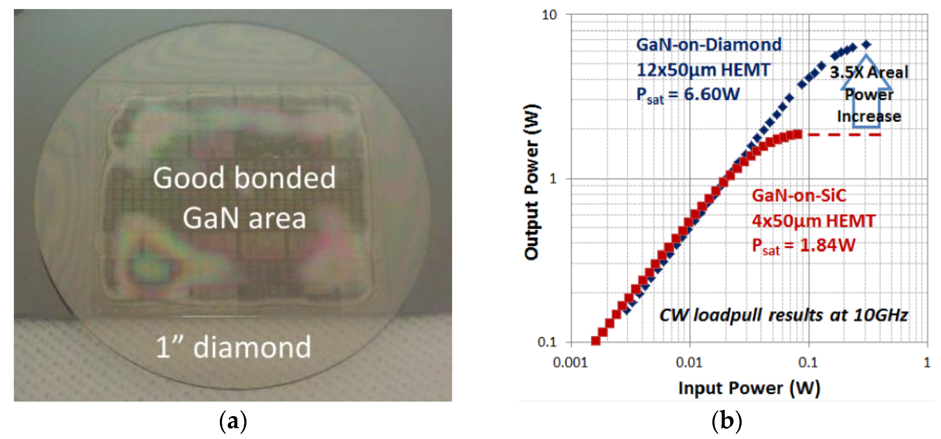
- Dumka, D.C.; Chou, T.M.; Faili, F.; Francis, D.; Ejeckam, F. AlGaN/GaN HEMTs on diamond substrate with over 7 W/mm output power density at 10 GHz. Electron. Lett. 2013, 49, 1298–1299. [Google Scholar] [CrossRef]


| Material Property | Si | SiC | GaN | Diamond |
|---|---|---|---|---|
| Bandgap (eV) | 1.12 | 2.9 (6H)/ 3.2 (4H) | 3.4 | 5.47 |
| Breakdown field (×106 V/cm) | 0.25 | 2.5 (6H)/ 3 (4H) | 3–3.75 | 20 |
| Electron mobility (cm2/(V⋅s)) | 1350 | 415 (6H)/ 950 (4H) | 1100–1300 | 2400 |
| Thermal conductivity (W/(m⋅K)) | 150 | 380–450 | 130–210 | 2200 (single crystal) >1800 (polycrystalline) |
| Coefficient of thermal expansion (×10−6 K−1) | 2.6 | 3.08 | 5.6 (a0)/ 3.2 (c0) | 0.8 |
| Material | Thermal Conductivity (W/(m⋅K)) |
|---|---|
| Sapphire | 46 |
| Si | 150 |
| SiC | 380–450 |
| Single-crystal diamond | 2200 |
| Polycrystalline diamond | >1800 |
| GaN | 130–210 |
| AlN | 130 |
| AlxGa1−xN | 10–11 |
| InxGa1−xN | 5–11 |
| SiN | 1.6 |
| Ref. | Year | Dielectric Layer | Diamond Film | TBRGaN/diamond (m2⋅K/GW) | ||
|---|---|---|---|---|---|---|
| Thickness (nm) | Material | CVD Type/Thickness (µm) | κ (W/(m⋅K)) | |||
| [63] | 2006 | -- | -- | HFCVD/25 | -- | -- |
| [66] | 2009 | -- | -- | 75 | -- | -- |
| [67] | 2010 | -- | -- | MPCVD/100 | >1500 | -- |
| [69] | 2013 | 40 | -- | 30 | -- | 36 ± 12 b |
| [70] | 2013 | 50 | -- | HFCVD/100 | -- | 18 a |
| [103] | 2014 | 30 | -- | 100 | -- | 29 ± 2 b |
| [72] | 2014 | 25 | -- | HFCVD/95 | 710 | 27 ± 3 a |
| 50 | MPCVD/120 | 1200 | 36 a | |||
| [77] | 2014 | 50 | -- | MPCVD/110 | 1200 | 17 b |
| 90 | 41 b | |||||
| [104] | 2014 | -- | -- | MPCVD | 1600 | 19 ± 3 b |
| [105] | 2014 | -- | -- | 100 | -- | 47.6 b |
| 19 b | ||||||
| [78] | 2015 | 34 | SiN | HFCVD/100 | 650 | 25 ± 3 b |
| 100 | MPCVD/100 | 1500 | 50 ± 5 b | |||
| 28 | MPCVD/100 | 1500 | 12 ± 2 b | |||
| [79] | 2016 | 40 | SiN | MPCVD/100 | 1370 | 25.5 ± 0.5 b |
| 31.0 ± 0.7 b | ||||||
| [80] | 2017 | 31 | SiN | HFCVD/100 | -- | 31.8 ± 5.3 b |
| 22 | SiN | MPCVD/100 | 19.8 ± 4.1 b | |||
| 17.4 ± 3.0 b | ||||||
| [81] | 2017 | 30 | SiN | MPCVD/100 | -- | 23 ± 3 b |
| [82] | 2017 | 5 | SiN | MPCVD/1 | 100–700 | 6.5 b |
| AlN | 15.9 b | |||||
| No interlayer | 61.1 b | |||||
| [10] | 2018 | 5 | SiN | MPCVD/1 | -- | 9.5 + 3.8/−1.7 b |
| AlN | 18.2 + 1.5/−3.6 b | |||||
| No interlayer | 41.4 + 14.0/−12.3 b | |||||
| [83] | 2019 | 100 | SiN | MPCVD/2 | -- | 38.5 ± 2.4 b |
| 100 | AlN | 56.4 ± 5.5 b | ||||
| [102] | 2019 | 35 | SiN | MPCVD/120 | -- | 31.0 ± 3.1 b |
| [99] | 2019 | 50 | SiN | MPCVD/100 | -- | 33 |
| 36 | SiN | 22 | ||||
| 41 | SiN | 15 | ||||
| [88] | 2019 | 36 | SiN | MPCVD/75 | -- | 20 c |
| 17 | 13 c | |||||
| [101] | 2019 | 30 | SiN | MPCVD/100 | -- | 18 b |
| [106] | 2020 | 20 | Al0.32Ga0.68N | MPCVD/35 | -- | 30 ± 5 b |
| Ref. | Year | Adhesive Layer | Diamond Substrate | Bonding Process | TBR (m2⋅K/GW) | |
|---|---|---|---|---|---|---|
| Thickness (nm) | Material | |||||
| [107] | 2013 | -- | Si-based | 1″ × 1″ PCD | Pressing at RT | -- |
| [109] | 2014 | 35 | Si-based | 1″ PCD wafer | Pressing <150 °C | 34 ± 5 a |
| [112] | 2017 | 30–40 | -- | 3″ PCD wafer | Pressing 180 °C | 51 b |
| [113] | 2018 | 24 | Si | 900 µm-thick PCD on Si | SAB RT | -- |
| [114] | 2019 | 6 | Si | 1 cm × 1 cm SCD | SAB RT | -- |
| [115] | 2020 | 10 | Si | SCD | SAB RT | 19 a |
| 2 | 11 a | |||||
| [117] | 2020 | 2 × 5/11 | Mo/Au | PCD/SCD | SAB RT | -- |
| [118] | 2020 | 10 | Ti/Si | 5 mm × 5 mm SCD | SAB RT | 66 c |
| [119] | 2020 | 2 × 450 | AlN | -- | SAB 160 °C | -- |
| [122] | 2018 | No interlayer | SCD | VdW bonding | 10 d | |
| Ref. | Year | Diamond | GaN | |||
|---|---|---|---|---|---|---|
| Deposition Method | Type | Thickness (µm) | Disl. Dens. (cm−2) | |||
| [125] | 2003 | Natural SCD | MOCVD on 10 nm AlN layer + HVPE | Polycryst. | 2.5 | -- |
| [126] | 2011 | (011) SCD | MOCVD on AlN layer | Polycryst. | 0.07–1.55 | -- |
| [127] | 2009 | (111) SCD | NH3-MBE on 100 nm AlN layer | Epilayer | 1 | -- |
| [128,129] | 2010 | (111) SCD | NH3-MBE on 200 nm AlN + GaN strain engineered interlayers | Epilayer | 0.8 | 8.4 × 10⁹ |
| [130] | 2011 | Ib (111) SCD | MOVPE on 180 nm single crystal AlN + 400 nm AlN/GaN | Epilayer | 0.6 | -- |
| [131] | 2012 | IIa (111) SCD | MOVPE on 180 nm single crystal AlN + 500 nm AlN/GaN | Epilayer | 0.6 | 8.4 × 10⁹ |
| [132,133] | 2012 | Ib (111) SCD | MOVPE on 180 nm single crystal AlN + 500 nm AlN/GaN | Epilayer | 0.6 | -- |
| [134] | 2009 | NCD | MOCVD on 50 nm GaN | Polycryst. | 3 | -- |
| [135] | 2010 | PCD | MOCVD | Polycryst. | 0.8 | -- |
| [124] | 2015 | PCD | MOVPE on 70 nm AlN layer + deposition of SiN stripes/etching + ELO | 15 µm wide epilayer | 1.5 | ≈7 × 10⁻⁹ → <108 |
| [136] | 2017 | PCD thin films | Etching of Si substrate + MOVPE on 10–40 nm AlN/Al0.75Ga0.25N layers | Epilayer | 0.2–1.1 | -- |
| [137] | 2020 | Post-deposited PCD | MOCVD of SiN-capped AlGaN/GaN stack on Si + selective deposition of PCD stripes + ELO | 5 µm wide epilayer | ≈1–5 | ≈109 → ≈107 |
| Ref. | Year | Passivation Layer | Diamond Film | TBR (m2⋅K/GW) | |||
|---|---|---|---|---|---|---|---|
| Thickness (nm) | Material | Thickness/Type (µm) | Dep. Temp. (°C) | CVD Type | |||
| [46] | 2001 | -- | SiN | 0.7–2/PCD | <500 | MPCVD | -- |
| [141,142] | 2010, 2012 | 50 | SiO2 | 0.5/NCD | 750 | MPCVD | -- |
| [143] | 2013 | No interlayer | -- | --/NCD | 750 | MPCVD | -- |
| [146] | 2017 | 10 | SiN | 0.5/NCD | 750 | MPCVD | -- |
| [148] | 2011 | -- | SiO2/Si3N4 | 0.5/NCD | 750–800 | HFCVD | -- |
| [149] | 2014 | -- | Si3N4 | 2.8/NCD | 750–800 | HFCVD | -- |
| [150] | 2017 | 50 | Si3N4 | 0.155–1/PCD | 650 | MPCVD | 45 + 13/–11—91 + 13/−9 a |
| [91] | 2019 | 46 | SiN | 1.46/PCD | 720–750 | HFCVD | 52.8 + 5.1/−3.2 a |
| [152] | 2019 | 30 | SiN | 3/PCD | 820 | MPCVD | -- |
| [154] | 2021 | 100 | SiN | 2.5/PCD | 700 | HFCVD | -- |
| GaN-on-Diamond | Bonded Wafers | GaN Epitaxy | Capping Diamond | |||
|---|---|---|---|---|---|---|
| SCD | PCD | SCD | PCD | |||
| Large area | Yes | No | Yes | No | Yes | Yes |
| κdiamond at interface | Low | High | High | High | ELO GaN-after-PCD: high | Low |
| PCD-after-ELO GaN: evaluation required | ||||||
| TBRGaN/diamond | Large | Small | VdW: not reproducible | Evaluation required | ELO GaN-after-PCD: evaluation required | Large |
| SAB: evaluation required | PCD-after-ELO GaN: evaluation required | |||||
| Removal of AlGaN/GaN stress-relief layers | Possible | Possible | Possible | Not possible | ELO GaN-after-PCD: not possible | Not relevant |
| PCD-after-ELO GaN: possible | ||||||
| AlGaN top barrier layer | Not relevant | Not relevant | Not relevant | Not relevant | Not relevant | Present |
| Induced thermal stress | Relevant | Not relevant | Not relevant | Not relevant | ELO GaN-after-PCD: not relevant | Relevant |
| PCD-after-ELO GaN: evaluation required | ||||||
| Manufacturing complexity | Fair | Fair | Fair | Simple | ELO GaN-after-PCD: fair | Simple |
| PCD-after-ELO GaN: complex | ||||||
| Advantage | |
| Limitation | |
| Severe limitation |
Publisher’s Note: MDPI stays neutral with regard to jurisdictional claims in published maps and institutional affiliations. |
© 2022 by the authors. Licensee MDPI, Basel, Switzerland. This article is an open access article distributed under the terms and conditions of the Creative Commons Attribution (CC BY) license (https://creativecommons.org/licenses/by/4.0/).
Share and Cite
Mendes, J.C.; Liehr, M.; Li, C. Diamond/GaN HEMTs: Where from and Where to? Materials 2022, 15, 415. https://doi.org/10.3390/ma15020415
Mendes JC, Liehr M, Li C. Diamond/GaN HEMTs: Where from and Where to? Materials. 2022; 15(2):415. https://doi.org/10.3390/ma15020415
Chicago/Turabian StyleMendes, Joana C., Michael Liehr, and Changhui Li. 2022. "Diamond/GaN HEMTs: Where from and Where to?" Materials 15, no. 2: 415. https://doi.org/10.3390/ma15020415
APA StyleMendes, J. C., Liehr, M., & Li, C. (2022). Diamond/GaN HEMTs: Where from and Where to? Materials, 15(2), 415. https://doi.org/10.3390/ma15020415