Article

Electrical and Heat Distributions and Their Influence on the Mass Transfer during the Flash Spark Plasma Sintering of a Cu/Cr Nanocomposite: Experiments and Numerical Simulation

1
Center of Functional Nano-Ceramics, National University of Science and Technology “MISiS”, Leninskiy Prospekt 4, 119049 Moscow, Russia
2
Department of Materials Science and Engineering, Sharif University of Technology, Tehran 11155-9466, Iran
3
Research Laboratory of Scanning Probe Microscopy, Moscow Polytechnic University, B. Semenovskaya St. 38, 107023 Moscow, Russia
4
School of Chemistry and Physics and Centre for Materials Science, Queensland University of Technology, Brisbane 4000, Australia
5
Department of Chemical and Biomolecular Engineering, University of Notre Dame, Notre Dame, IN 46556, USA
*
Authors to whom correspondence should be addressed.
Materials 2022, 15(20), 7366; https://doi.org/10.3390/ma15207366
Submission received: 31 August 2022 / Revised: 16 October 2022 / Accepted: 18 October 2022 / Published: 20 October 2022
(This article belongs to the Special Issue Spark Plasma Sintered Materials with Advanced Properties)

Abstract

:
The nanocomposite Cu–Cr powder was consolidated by flash spark plasma sintering (FSPS), which involves applying an extremely rapid change in the electrical power passing through the bulk of the sample. It was demonstrated that an essentially fully dense material could be obtained in 15 s. Such short-term treatment typically preserves the nanostructured features of the material. However, investigation revealed a nonuniformity in the microstructure of the alloys obtained under such extreme conditions. To better understand the observed effects, the FSPS process was simulated. It was observed that a rapid change in the applied electrical power resulted in nonuniform distributions of current density and temperature along the body of the consolidated material. Specifically, the current density was higher on the periphery of the sample, and the temperature was higher in the middle. These findings explain the observed structural transformation during FSPS and suggest an optimization strategy to avoid microstructural nonuniformity.

Graphical Abstract

1. Introduction

Owing to their unique mechanical, thermal, and electrical properties, copper-chromium nanocomposites are used in a variety of applications, particularly as vacuum interrupters [1,2]. These materials, which are mostly fabricated using powder metallurgy techniques, are extremely sensitive to manufacturing factors [3,4]. For example, to maintain the required fine structure during the sintering procedure, they require a very low temperature and short heat treatment time. Indeed, when subjected to high temperatures for an extended period, these nanocomposites, which are typically formed via high-energy ball milling (HEBM), have a significant tendency to segregate constituent elements from each other, rapidly forming large copper and chromium grains [5,6]. Thus, conventional sintering processes are no longer a suitable option, and innovative methods must be employed to minimize the sintering time and temperature [7,8].
Some of the unique methods to produce Cu/Cr parts are additive manufacturing techniques, such as selective laser melting and selective electron beam melting [9,10,11]. However, because these approaches are intrinsically predicated on the melting of feedstock materials, they are incapable of retaining the nanostructured-supersaturated-solid solution of the initial powders owing to liquid phase segregation and spinodal decomposition. Another creative solution that has been considered for the manufacturing of these nanocomposites is spark plasma sintering (SPS). Several investigations have demonstrated that materials fabricated using this technology exhibit few microstructural changes and have improved mechanical, electrical, and thermal characteristics compared with those of the components produced using other approaches [4,12,13,14,15,16].
Flash sintering (FS) is one of the most recent methods for material consolidation based on the use of an electric field, known as field-assisted sintering technology, which was accidentally discovered in 2010 by Cologna et al. [17], who investigated the effect of electric current on the grain growth of yttrium-stabilized zirconia. Advantages, such as a very short processing time (less than one minute), which restricts grain growth and is critical in sintering nanostructured materials, have made this approach highly popular among scholars. Recently, there has been an increased interest in the investigations of the mass transfer processes during FS. Three primary hypothesized processes have been suggested: (1) Joule heating runaway [18,19], (2) electrochemical reactions [20,21], and (3) nucleation caused by the movement of charged defects [22,23].
In recent years, researchers have created other variations of this process based on the criteria supplied by its patentors, the most well-known of which is flash spark plasma sintering (FSPS). The FSPS principle is based on the modification of the sintering tooling to direct the majority of the applied current to the sample and prevent it from flowing through the die. During FSPS, the mass transfer mechanism of a material, particularly in electrically conductive systems, is generally regarded as localized Joule heating generated in the interparticle regions, resulting in specimen consolidation in a matter of seconds [24]. Using this concept, various materials such as ceramics [25,26,27,28], metals [3,29,30], and composites [31,32] have been successfully sintered regardless of whether they are electrical conductors or insulators. Using the FSPS approach, Sharma et al. [33] produced SiC samples and examined the effects of the electrical conductivity of various additives, namely an electrical conductor (TiC), a semiconductor (B4C), and an electrical insulator (Al2O3), on the sintering behavior of the manufactured parts. Optimum results were achieved when a semiconductor additive was used to facilitate the development of a liquid phase, resulting in the compaction of the specimens. The acceleration of ceramic material consolidation caused by the formation of a liquid phase was also found in the FSPS treatment of titanium diboride with a B2O3 addition [34].
In our previous studies [3,35], we discovered that using this technology can reduce the sintering time by 40 times and the energy consumption by more than 20 times while maintaining the same characteristics and microstructure. Several publications [36,37,38] have numerically modeled the FSPS process. However, the effects of a high heating rate and current density on the microstructural evaluation of these nanocomposites utilized in this approach are not well understood.
This study aims to investigate the microstructural evolution of Cu/Cr nanocomposites produced using FSPS. In this context, in addition to experimental data, numerical simulations were conducted to visualize the distribution of current and heat along the sintering body. Moreover, both the thermal and electro-induced segregation phenomena observed in the outcomes were evaluated from the thermodynamic and kinetic perspectives.

2. Materials and Methods

2.1. Powder Preparation

In this study, copper (99.9% purity, dendrite shape, Uralelektromed, Russia) and chromium (99.9% purity, elongated faceted type, Polema, Russia) powders with average particle sizes of 63 and 20 µm, respectively, were employed. The following mechanical process was used to prepare the Cu/Cr nanocomposite powder: The Cu and Cr powders in a mass ratio of 55% Cu to 45% Cr were poured into stainless steel jars. The ratio of the 8 mm stainless steel balls and the powder mixture was 20:1. The jar was vacuumed and pressurized with argon gas (4 atm.) to protect the mixture from oxidation throughout the milling operation. The HEBM operation was then conducted using a planetary ball mill Activator-2S (Activator, Russia) with a revolving speed of 694 rpm for both the sun wheel and the jar. The entire procedure involved four 15 min mills separated by 5 min cooling periods. The additional details of the preparation procedure and the microstructure of the nanocomposite powder can be found elsewhere [3].

2.2. Consolidation

Labox 650 (Sinter Land, Nagaoka, Japan) SPS equipment was used to consolidate the samples. Figure 1 shows a schematic of the sintering tooling used in the FSPS operations in this study. The Cu/Cr powder (3 g), prepared via HEBM, was placed into a graphite die with an internal radius of 13 mm, wall thickness of 10 mm, and height of 40 mm. The green nanocomposite powder was then cold-pressed under an external pressure of 50 MPa. The mechanical pressure applied to the samples was maintained throughout the sintering procedure. The atmospheric pressure inside the chamber was 10 Pa.
It is important to emphasize that the interior wall of the die was covered with an alumina layer (thickness: 0.3 mm) to prevent the electrical current from passing through the wall of the die. In addition, the specimen was enveloped in a graphite sheet (thickness: 0.4 mm) before being placed within the die. The absence of electrical conductivity between the sample and the die was confirmed using a multimeter. Therefore, electrical power could only pass through the specimen/graphite sheet configuration.
To consolidate the samples using the FSPS approach, the temperature was raised to 473 K at a heating rate of 100 K/min; thereafter, the power was abruptly boosted to the desired level and the device was turned off. In this study, the device powers used were 27% and 33%, corresponding to the power densities of 6.4 × 10⁶ and 9.3 × 10⁶ W/m2, respectively. Hereafter, “FSPS_1” refers to the sample generated using 27% power, while “FSPS_2” corresponds to the sample obtained using 33% power. It is worth noting that the variables such as voltage and applied current were captured at 1 s intervals during the process and were later used for numerical simulation. The total process duration from the increase of the electrical current to its complete termination was 15 s.
However, additional tests with longer dwell times were conducted using the FSPS scheme, and the data were used to validate the numerical results with experimental statistics. These tests were performed at a heating rate of 100 K/min to a maximum temperature of 973 K and a dwell time of 15 min. The temperature of the specimen was measured using K-type thermocouples positioned into holes 0.9 and 0.1 mm deep in the outside surface of the die and represented in Figure 1 by the names of points A and B, respectively.

2.3. Methods for Materials Characterization

Scanning electron microscopy (SEM, JEOL JSM-7600F) with energy-dispersive X-ray spectroscopy (EDS, Oxford Instruments X-MAX 80) was conducted to investigate the microstructures of the obtained alloys. The electrical resistance of the samples was measured using the four-contact method in DC (KRIOTEL Ltd., Moscow, Russia). In addition, an LFA457 NETZSCH thermal diffusion analyzer (Selb, Germany) was used to evaluate the thermal diffusivity of the specimens. Furthermore, the hardness of the samples was evaluated using a micro-hardness tester on polished micro-sections (CSM Instruments, Peuseux, Switzerland) by the Oliver and Farr method, which allows determining this characteristic by analyzing the resulting load-displacement curves. A diamond pyramid was used as the indenter (Vickers hardness test), the maximum load was 100 mN, and the duration of a single loading–unloading cycle was 72 s.

2.4. Numerical Simulation

2.4.1. Governing Equations

To simulate the FSPS, the COMSOL Multiphysics® software package was used to couple the thermal and electrical equations [39,40,41]. Maxwell’s equations describe the electric field in the system, as follows:
J = ( σ E ) = ( σ U ) = 0
where J, σ, E, and U are the current density, electrical conductivity, electric field, and electric potential, respectively.
The energy equation in the cylindrical form was used, as follows:
ρ c p T t = 1 r r ( r λ r T r ) + 1 z z ( r λ z T z ) + q i
In the above equation, r and z indicate directions; T is the temperature; and λ, ρ , and c p are the thermal conductivity, density, and heat capacity of the selected materials, respectively. The primary expressions in this equation are the heat conduction equations arising from the thermal gradient, and electric field equations, which characterize the flow of current across a conductive medium.
Furthermore, q i refers to Joule heat, which is calculated as:
q i = J . E
The electric current equation in the cylindrical form is as follows:
1 r ( r J r ) r = J z z
where Jr and Jz indicate the current densities in the radial and axial directions, respectively.
To account for the power dissipation in the heating tools, the root mean square should be defined for the current density and voltage, which is given by Equation (5), where u ,   P , and τ are the instantaneous voltage, pulsed DC period, and time, respectively.
U R M S = 1 P t T t u 2 ( τ ) d τ
Table 1 lists the physical characteristics of the different materials used in the numerical computations in this study.

2.4.2. Initial and Boundary Conditions
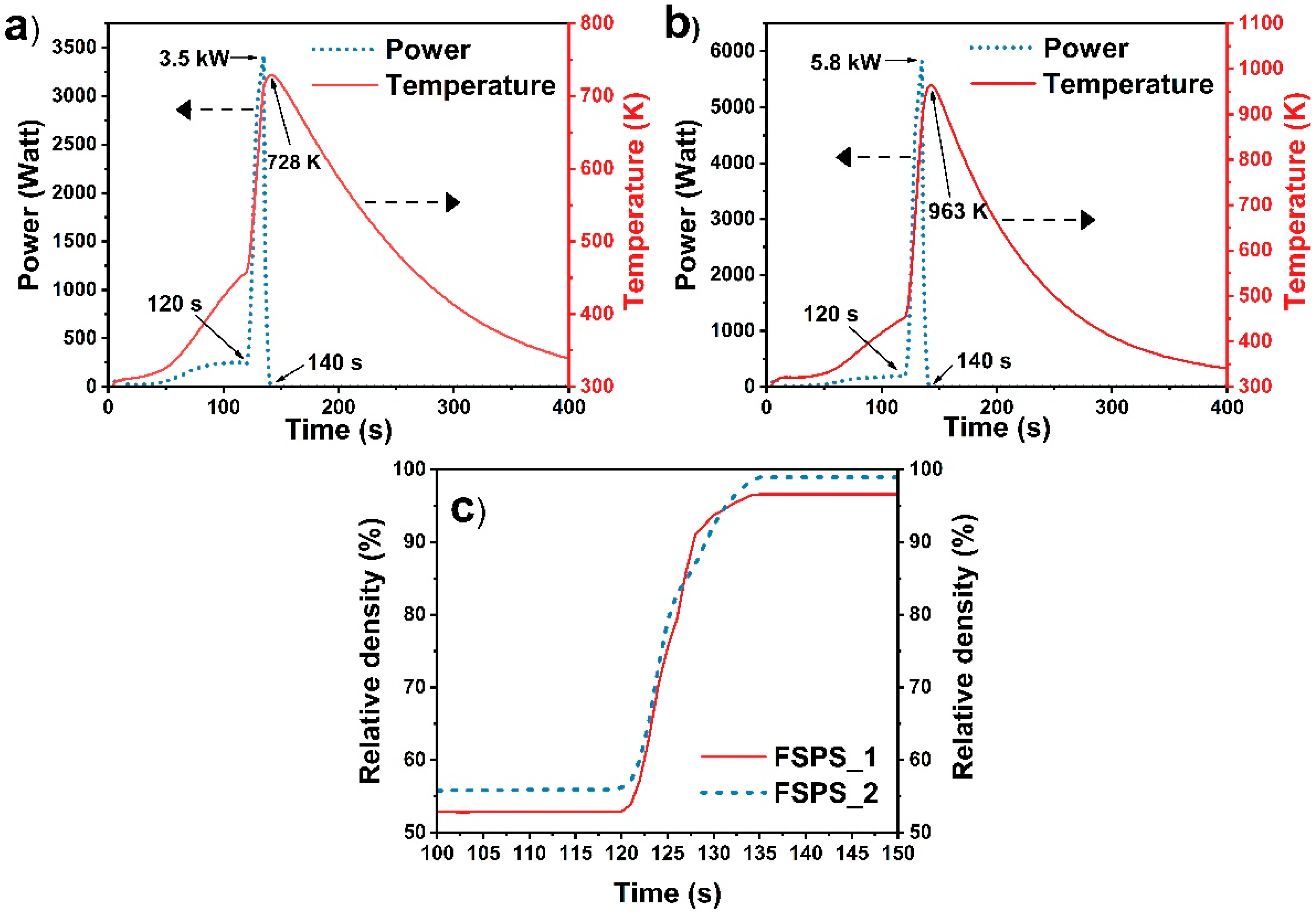
The initial temperature within the SPS chamber was 300 K, and the electric potential was zero at t = 0. The exterior surfaces of the sintering tooling were assumed to be electrically isolated. An electrical current was applied from the top plunger, while the bottom of the lower plunger was treated as the ground. At both the upper and lower surfaces, the convective heat transfer coefficient of 880 W m 2 K was used [46]. The convective heat dissipation from the sintering tooling on the lateral sides was neglected because the entire setup was confined within a vacuum chamber. Therefore, we considered only the radiation heat dissipation:
q r = σ s ε ( T e 4 T a 4 )
where the emissivities ( ε ) for graphite and Inconel are 0.8 and 0.67 [47], respectively; σ s is the Stefan–Boltzmann constant; and T e and T a are the surface temperatures of the graphite die and punch and the temperature of the chamber walls, respectively.

3. Results

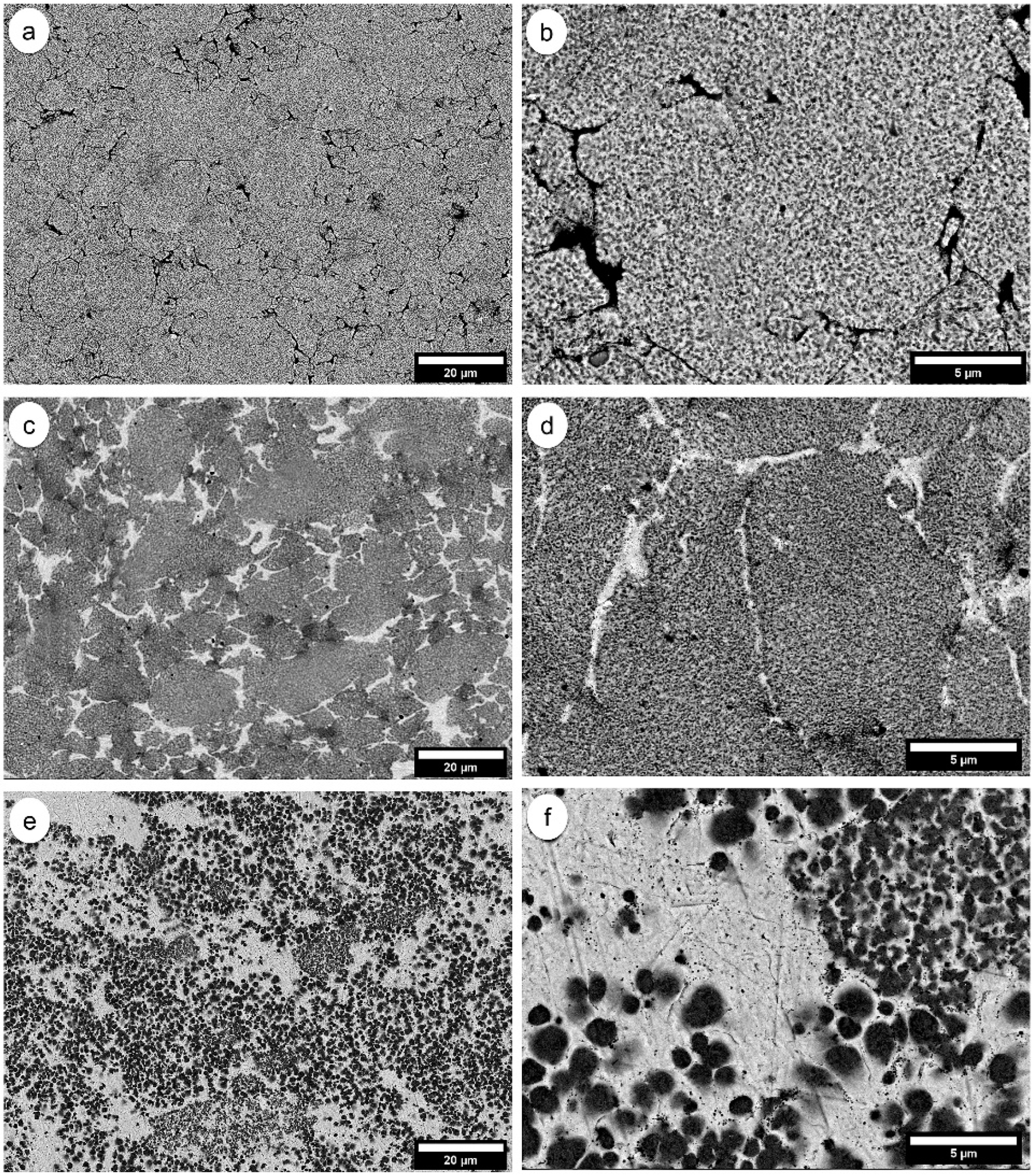
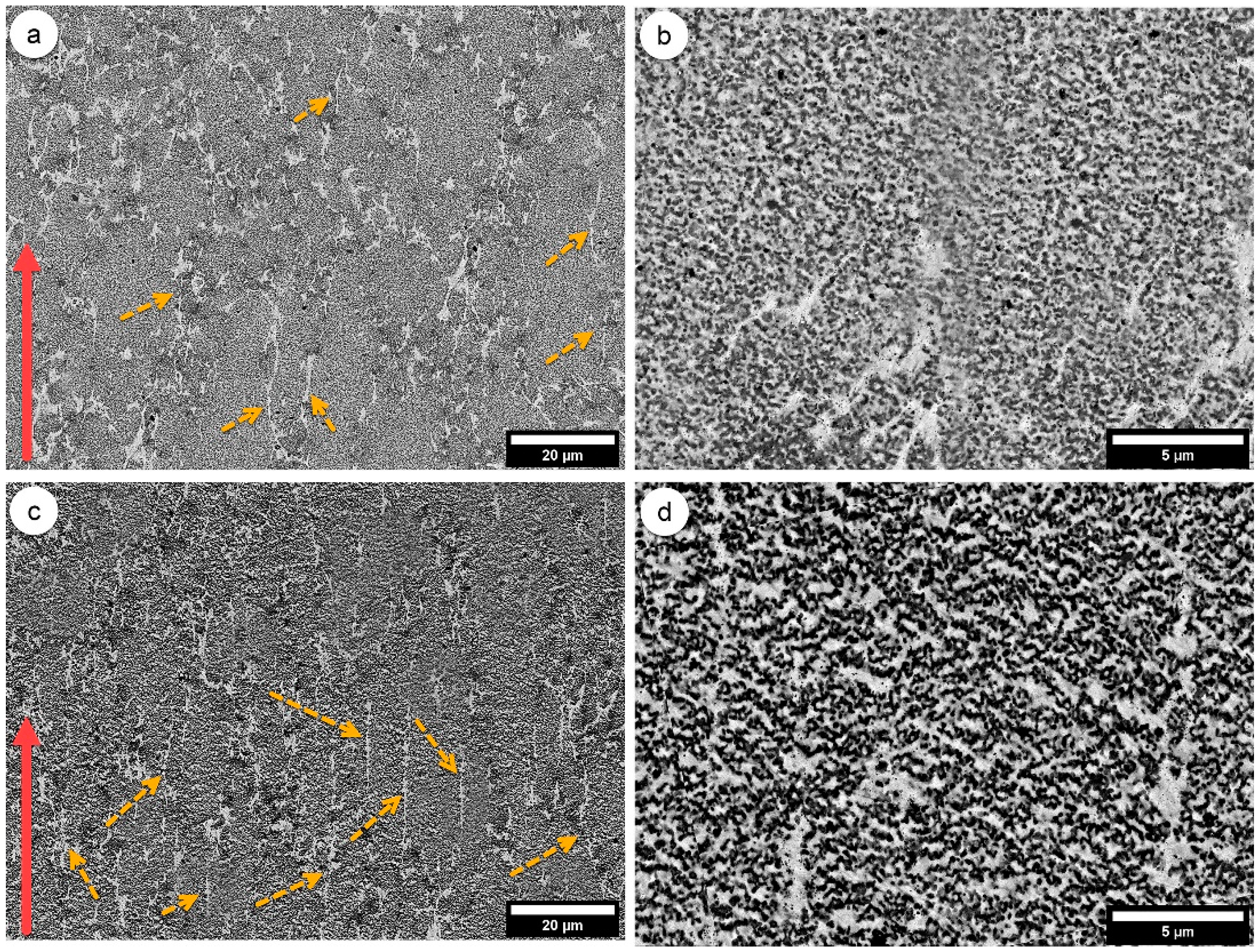
3.1. Experimental Studies

The typical densification parameters of FSPS_1 and FSPS_2 samples are shown in Figure 2. The initial stage (~120 s) involved preheating the samples at a rate of 100 K/min to approximately 473 K (Figure 2a,b). This stage was followed by a rapid increase (in 15 s) in electrical power through the samples (up to 3.5 and 5.8 kW for FSPS_1 and FSPS_2, respectively), which resulted in a rapid (~2000 K/min) increase in the temperature to its maximum value (728 and 963 K for FSPS_1 and FSPS_2, respectively). The total duration of the process after the rapid increase in electrical power until it was completely switched off was 20 s in both cases.
The consolidation of the material rapidly occured (Figure 2c), reaching the final relative densities of 97 ± 0.2% and 99 ± 0.3% for FSPS_1 and FSPS_2, respectively. Because the rates of power increase and heating were extremely fast, the question was whether the distribution of the current and temperature could be expected to be uniform along the sample cross-section. The latter might influence the uniformity of the consolidated material microstructure.
Figure 3 shows the microstructures of the centers of the samples produced via FSPS under different conditions. Figure 3a,b depict the microstructure of the sample core heated at a rate of 100 K/min to 475 K and then quenched. It could be observed that sintering did not occur between the nanocomposite particles until that moment, while the intergranular porosity slightly decreased under an applied external pressure and an elevated temperature (Figure 3a). Each composite Cu/Cr particle (Figure 3b), fabricated via HEBM, contained nanosized (5–10 nm) grains of Cr (dark phase) and Cu (bright phase). This can be considered the initial microstructure before the FSPS process was applied.
After FSPS under condition mentioned for FSPS_1 (Figure 3c,d), the microstructure changed, i.e., the porosity significantly decreased, and the Cu/Cr composite particles were then surrounded by Cu layers (light phase). However, when the sample was consolidated under the condition noted for FSPS_2, the microstructure in the center of the sample significantly changed (Figure 3e,f). The structure lost the “memory” of the initially nanostructured Cu/Cr particles and involved the spherical submicron Cr grains dispersed throughout the Cu matrix.
The structures of the edges of the samples are shown in Figure 4. The microstructure of FSPS_1 (Figure 4a,b) slightly differed from that of the center. This is because the thickness of the Cu-rich layers between the composite grains was lower (compare Figure 3c and Figure 4a) and because these layers displayed a different texture (see Figure 4a). This effect was more pronounced for the microstructures of the edges of FSPS_2 (Figure 4c,d). Moreover, a close examination showed that the preferable orientations of these layers were parallel to the direction of the applied electrical field (indicated by the red arrow in Figure 4a,c). Overall, for both cases, while the nanostructured Cu/Cr grains looked similar to those of the initial sample, the Cu-rich layers were aligned in a direction parallel to the direction of the applied field.

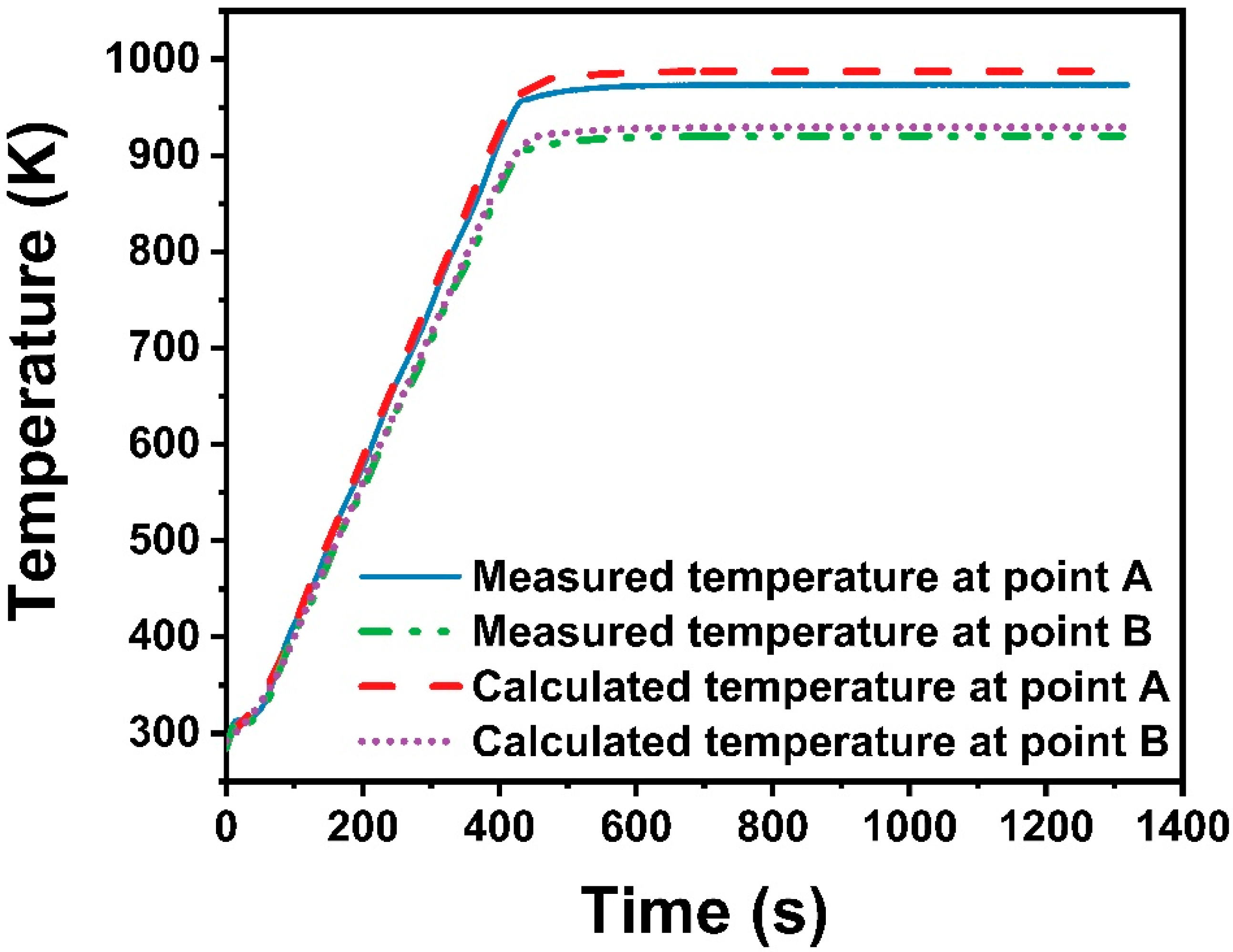
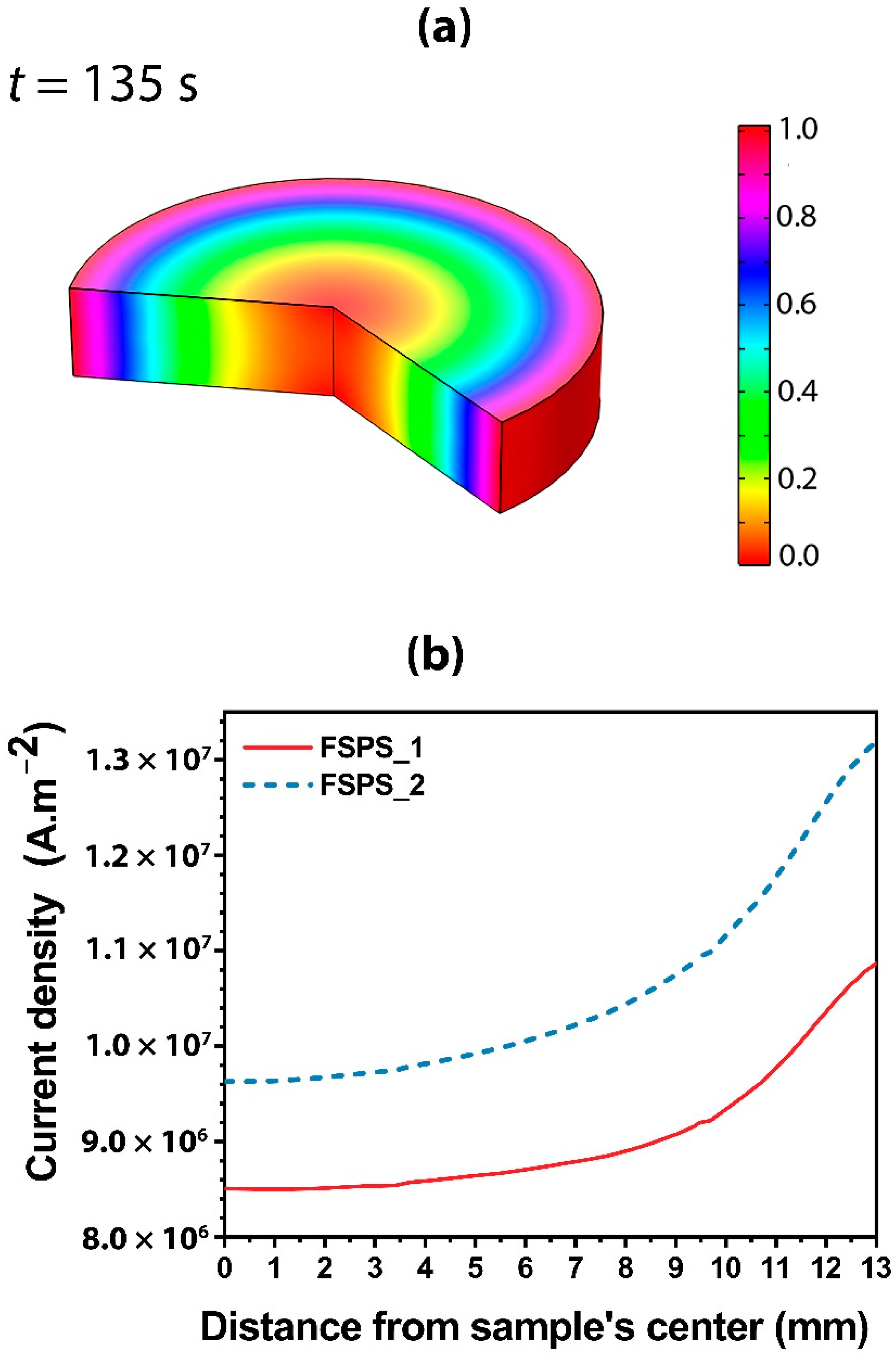
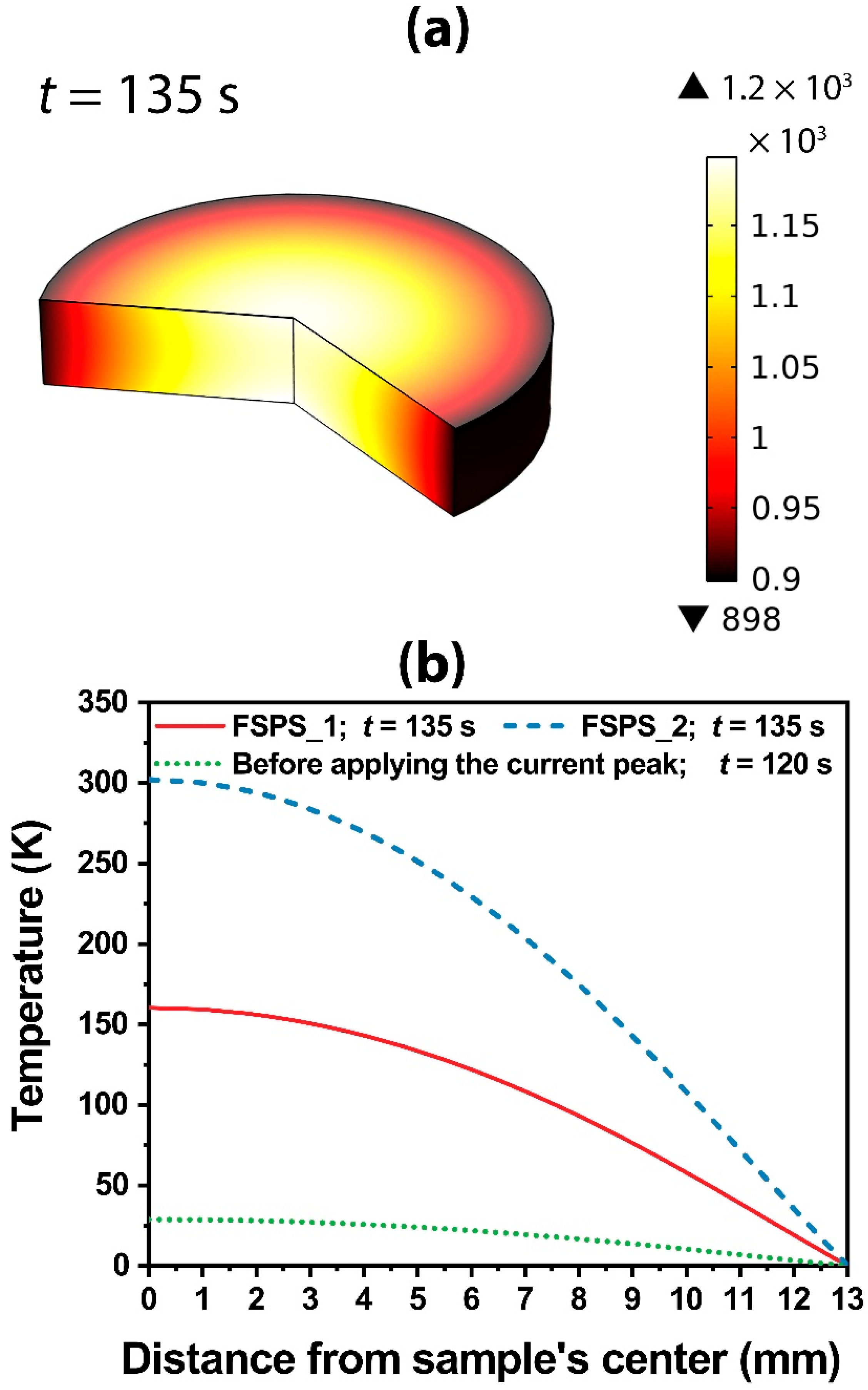
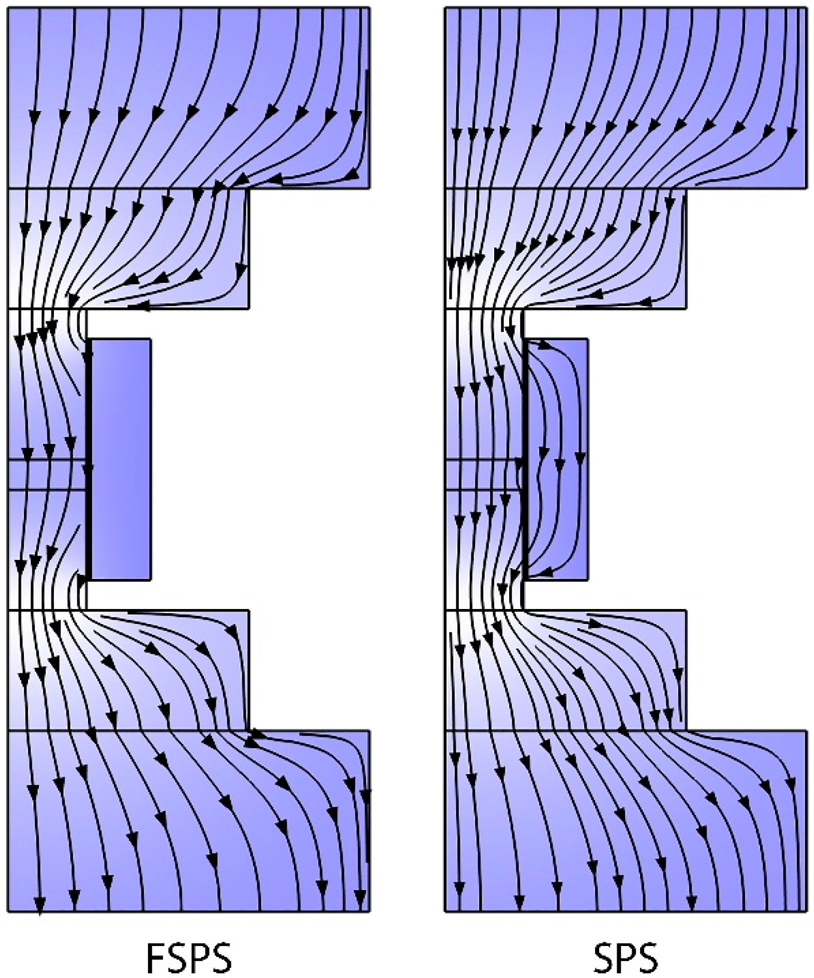
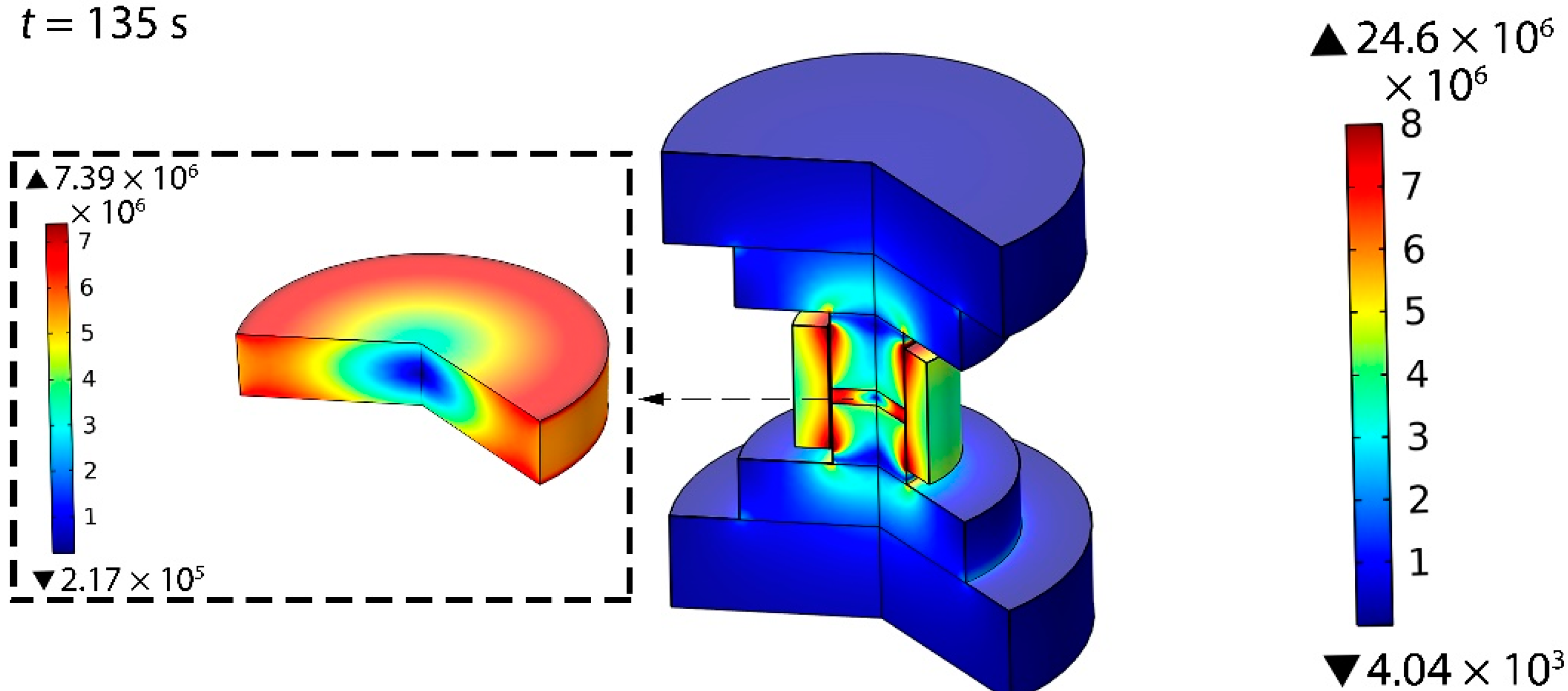
3.2. Simulation Results
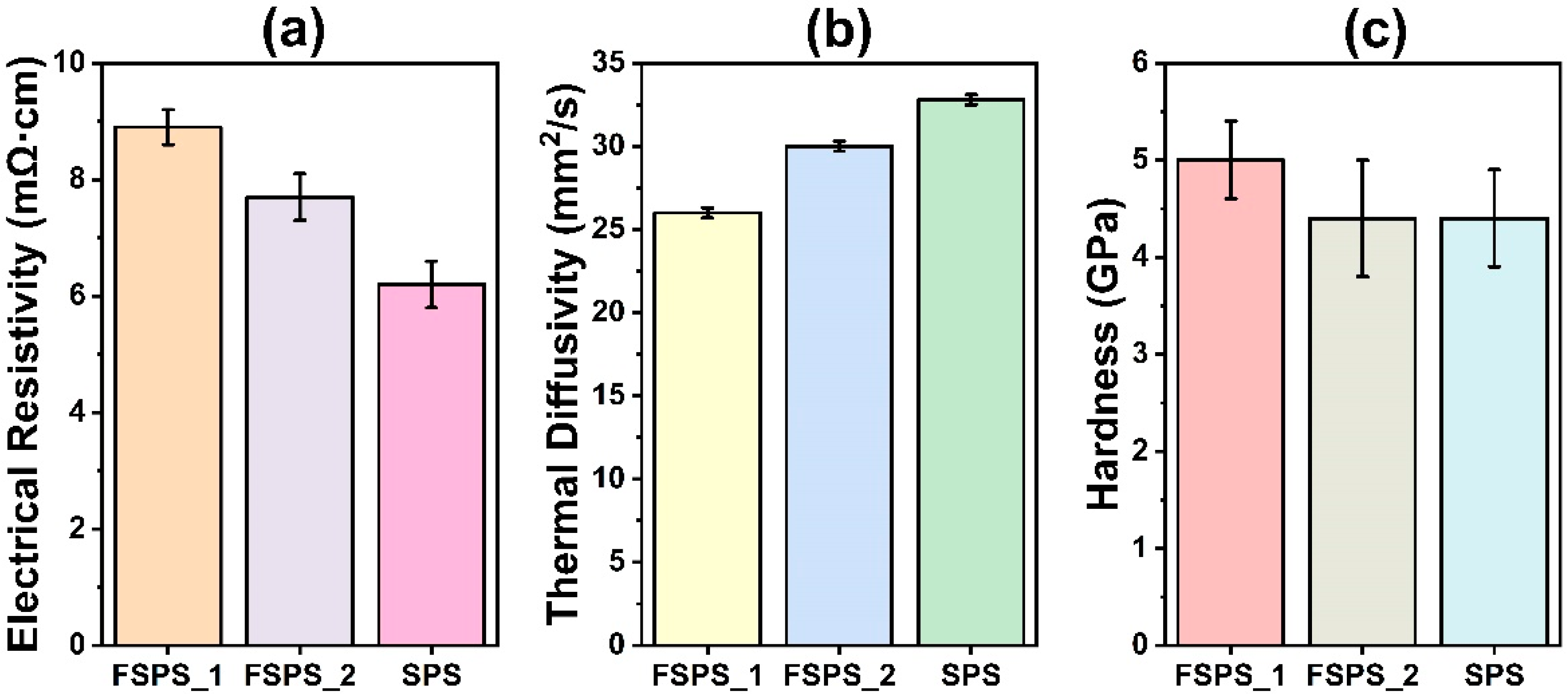
To understand the above experimental observations, it is important to know the current and temperature distributions along the volume of the sample during FSPS. However, these parameters are difficult to address experimentally. First, measuring the precise temperature of the sample is challenging, because the temperature was recorded in a hole in the lateral surface of the die and thus it might be different from the temperature in the center of the specimen. It is worth noting that the nonuniformity of the temperature distribution intensified with an increasing heating rate, which was rooted in the reduction in the characteristic time of thermal equilibrium. Second, currently, we do not have diagnostics for measuring electrical current distribution along the cross-section of the sample. This emphasizes the significance of modeling the temperature and current distribution for the FSPS process, which has a heating rate order of magnitude higher than that of conventional SPS.
To validate the theoretical model (see Section 2.3), we first calculated the temperature-time profiles at points A and B (see Figure 1) under the conditions described in Section 2.2 and compared them with the experimentally measured profiles. Figure 5 shows the results of these comparisons. It can be observed that the numerical and experimental results were in good agreement. Subsequently, we applied the model to simulate the FSPS in the Cu/Cr system.
The determination of the electrical current density inside a sample during FSPS allowed not only an evaluation of the average heat (temperature) distribution along the body but also enabled the identification of the microstructural features that were more prone to electric-current-induced mass transport processes. This feature was mainly affected by three factors: geometry, thermal and electrical conductivities of the structural constituents of the sample, and sintering tooling. Figure 6a depicts the calculated dimensionless current density ( θ = J J min J max J min ) at the end of the experiment (t = 135 s; see Figure 2a,b) for the sintered Cu/Cr nanocomposites.
During FSPS, a considerable disparity in the current distribution within the sample occurred: the edges of the sample had the maximum θ, which gradually decreased until it reached the lowest value in the center of the sample.
Figure 6b depicts the current density values as a function of the radial distance from the specimen center for both samples FSPS_1 and FSPS_2. Although both specimens exhibited a similar trend in the current density distribution in the radial direction, FSPS_2 was subjected to a larger current density. In the case of FSPS_2, the minimum current density was 9.6 × 10⁶ A/m2 and the maximum was 1.32 × 10⁷ A/m2, whereas in FSPS_1, the values were 8.5 × 10⁶ A/m2 and 1.1 × 10⁷ A/m2, respectively.
The current density distribution within the sample obtained in this study was in good agreement with the numerical simulations and experimental results reported for conductive materials [48].
The corresponding calculated temperature distribution for FSPS_2 (at the end of the process, t = 135 s; see Figure 2c) is shown in Figure 7a.
The maximum temperature of ~1200 K appeared to be in the center of the specimen, whereas the edges had the lowest temperature of ~898 K. The radial temperature differences for both FSPS conditions and their values before applying the peak current amplitude (t = 120 s) are shown in Figure 7b. There was a temperature differential of approximately 25 K between the center and edges of the sample at t = 120 s, just before delivering the peak of the current amplitude. As the applied electrical power approached its maximum, the radial temperature difference considerably increased, reaching 160 and 300 K at the end of the operation for samples FSPS_1 and FSPS_2, respectively.
It is logical to expect a direct correlation between the current density and temperature distribution inside the sample, implying that the higher the current density, the more heat is generated. However, this logic applies to adiabatic conditions. The simulation demonstrated that this was not the case under the applied FSPS conditions. To understand this effect, we first considered the difference in boundary conditions for conventional SPS and FSPS.
In the conventional SPS of an electrically conductive specimen, the electric current passes through the die and sample (proportional to the electrical conductivity of each component); consequently, in the case of FSPS, the current does not pass through the graphite die. Figure 8 illustrates the differences in current transmission streamlines between these configurations.
Thus, in the SPS scheme, radiation from the sintering tooling surfaces is the main source of heat dissipation. However, in the FSPS scheme employed in this study, the flow of electric current through the die was blocked, resulting in the die acting as a cooling wall. Figure 9 shows the energy flux within the sample. Maximum heat loss occured at the edges of the sample. This extreme heat dissipation in the radial direction explained why the edges of the sample had the lowest temperature despite the fact that they transmited the maximum current density.

3.3. Properties

The electrical resistivity, thermal diffusivity, and hardness of the produced samples are compared in Figure 10. These characteristics were compared with the corresponding values reported previously [3] for a sample produced under SPS conditions, i.e., a temperature of 1123 K and heating rate of 100 K/min. It could be seen that the specimens manufactured by the FSPS approach had improved properties compared with those produced under SPS condition. It is also worth noting that the FSPS approach required substantially less processing time and energy consumption. Furthermore, the electrical resistivity and hardness of FSPS_1 were higher than those of FSPS_2, whereas FSPS_2 had a higher thermal diffusivity than that of FSPS_1. This behavior was due to the differences in the microstructures of these specimens. The electrical and thermal conductivities of Cu are lower than those of Cr. Therefore, larger Cu-rich areas in FSPS_2, compared with FSPS_1, resulted in lower electrical resistance and higher thermal diffusivity, and vice versa. Moreover, a sample that retains its nanostructure during the sintering process will have a higher hardness [49,50,51]. As shown in Figure 3 and Figure 4, FSPS_1 had a homogeneous nanostructure at its center and edges, while the grain size in the center of FSPS_2 was in the micron and sub-micron range; therefore, the hardness of FSPS_2 was lower than that of FSPS_1.

4. Discussion

With a better understanding of the temperature distribution inside the sample during the FSPS process of the Cu/Cr nanocomposite, we can explain the microstructural transformations observed during the FSPS of the samples (Figure 3 and Figure 4) from a thermodynamic and kinetic standpoint.
The main issue to be addressed is how the Cu-rich layers are formed during FSPS. Cu–Cr is known to be an immiscible alloy, implying very poor (basically zero) solubility of one element in another. Using a kinetic perspective would suggest that a self-diffusion process is responsible for mass transport at the micro-level in this type of medium. Cu and Cr have the self-diffusion coefficients D C u and D C r , respectively, as shown in the equations below [52,53]:
D C u = 4.68 × 10 5 exp ( 47140 R T )
D C r = 2 × 10 5 exp ( 73700 R T )
where R is the ideal gas constant in cal/mol.K, T is the temperature in K, and the activation energy is given in cal/mol. The calculated diffusion coefficients for Cu and Cr at a temperature of 1200 K were equal to 1.2 × 10⁻¹³ and 7.5 × 10⁻¹⁹ m2/s, respectively. As a result, Cu diffused considerably faster than Cr. Consequently, phase segregation occured at the microscopic level inside the sample.
The next question is: how does the electric current passing through the media affect the mass transfer mechanism? The effect of electric current on mass transport in metals is a complex phenomenon and results from a contribution of various factors, such as electromigration, localized overheating at interparticle regions, and particle size. We recently investigated the influence of electric current on diffusion kinetics of a Ni–Al system by using a diffusion couple [29]. It was experimentally demonstrated that SPS conditions significantly enhanced the diffusion phenomena as compared to an alternative preheating technique that did not apply an electric current to the component throughout the process. More specifically, the effective activation energy of diffusion dropped almost two times under Joule heating conditions. Similar trends have been reported in several studies [54,55,56,57]. Therefore, it was expected that a similar effect would occur for the Cu–Cr system.
It is worth mentioning that in many previous publications, it has been stated that the electromigration phenomenon might intensify mass transfer caused by the direct application of an electric current to a sample. Current densities higher than 107 A/m2 and high average atomic mobilities are desirable for accelerating mass transfer through electromigration [58]. In our previous work [29], we considered the electromigration rate to investigate the potential contribution of electromigration to mass transfer for a Ni–Al system under SPS conditions. It was demonstrated that a current density several orders of magnitude higher than that employed in SPS studies was required in order to effectively accelerate the diffusion process through electromigration. Hence, it can be concluded that electromigration does not have a substantial influence on increasing the mass transfer phenomenon during SPS-based processes (including FSPS-based ones).
Hence, if we consider the micro-mechanism for mass transfer in the composite Cu/Cr particles during FSPS, we propose that the self-diffusion of metals dominates with a much faster rate for Cu. This prediction is supported by our observations regarding the changes in the microstructure during SPS consolidation [3]. However, the high heating rates during FSPS may lead to more pronounced local overheating of the media in the contact areas, leading to partial melting and intensification of the mass transport [59,60].

5. Conclusions

It was shown that FSPS is an extremely fast, energy- and time-saving method for the consolidation of materials, specifically immiscible Cu/Cr alloys. The direct comparisons between the experimental data reported in [3] and those in this study showed that fabricating pore-free materials required minutes for conventional SPS and only 15 s for the FSPS mode. In addition, a shorter sintering time allowed for better preservation of the nanostructure of the considered material, which led to improved mechanical properties (see [3] for details). However, according to the experimental and computational data reported in this study, the FSPS technique belongs to the category of sintering methods that are extremely sensitive to their processing parameters. An extremely fast heating rate (thousands of Kelvin per minute), which leads to exceptionally rapid consolidation, may also result in the nonuniformity of the temperature distribution along the sample volume. This implies that the optimal sample sintering conditions, including the amplitude of the electric current and processing duration, are to be precisely determined to minimize possible microstructural and compositional heterogeneities. For example, the heating rate of 50 K/s (FSPS_2) resulted in a significant segregation of the phase in the middle of the sample, whereas the FSPS at a rate of 35 K/s (FSPS_1) resulted in only minor differences (compare Figure 3 and Figure 4). In addition, our study suggested that it is important to optimize the temperature of the surroundings (e.g., the graphite die), which defines heat dissipation. On the one hand, it should not be excessively high, which may lead to a much higher temperature along the outer volume of the sample. On the other hand, it should not be excessively low either, leading to the opposite effect, as demonstrated in this study.

Author Contributions

Conceptualization, M.A. and A.M.; methodology, M.A., A.A. and S.S.; software, M.A. and A.A.; validation, M.A. and K.O.; formal analysis, M.A. and A.A.; investigation, M.A., A.A. and S.S.; resources, M.A. and D.M.; data curation, M.A. and A.M.; writing—original draft preparation, M.A.; writing—review and editing, M.A., K.O. and A.M.; visualization, M.A. and A.A.; supervision, A.M.; project administration, M.A. and A.M.; funding acquisition, D.M. and A.M. All authors have read and agreed to the published version of the manuscript.

Funding

This research received no external funding.

Institutional Review Board Statement

Not applicable.

Informed Consent Statement

Not applicable.

Data Availability Statement

Not applicable.

Acknowledgments

We would like to express our gratitude to Mobina Abedi for her invaluable assistance in the preparation of the artwork for this article.

Conflicts of Interest

The authors declare no conflict of interest.

Nomenclature

c p heat capacity, J/K
d diameter, m
D diffusion coefficient, m2/s
E electric field, V/m
J current density, A/m2
J r current density in a radial direction, A/m2
J z current density in an axial direction, A/m2
P pulsed DC period, s
q i Joule heating, J
q r radiation heat dissipation, W
r radial direction
R gas constant, cal/mol.K
T temperature, K
T a temperature of the chamber walls, K
T e surface temperature of the graphite die and punch, K
u instantaneous voltage, V
U electric potential, V
U R M S root mean square of the value of the voltage, V
z axial direction
Greek symbols
α thermal diffusivity, m2/s
ε material emissivity
λ thermal conductivity, W/m.K
ρ theoretical density, kg/m3
ρ e electrical resistivity, Ω⋅m
τ time, s
σ electrical conductivity, S/m
σ s Stefan–Boltzmann constant, W/m2.K4
Non-Dimensional Numbers
θ dimensionless current density; ( J J min J max J min )
Acronyms and abbreviations
DCDirect Current
EDSEnergy-Dispersive X-ray Spectroscopy
FSFlash Sintering
FSPSFlash Spark Plasma Sintering
HEBMHigh-Energy Ball Milling
SEMScanning Electron Microscopy
SPSSpark Plasma Sintering

References

  1. Slade, P.G. The Vacuum Interrupter: Theory, Design, and Application, 2nd ed.; CRC Press: Boca Raton, FL, USA, 2020; 666p. [Google Scholar] [CrossRef]
  2. Abedi, M.; Asadi, A.; Vorotilo, S.; Mukasyan, A.S. A critical review on spark plasma sintering of copper and its alloys. J. Mater. Sci. 2021, 56, 19739–19766. [Google Scholar] [CrossRef]
  3. Kuskov, K.V.; Abedi, M.; Moskovskikh, D.O.; Serhiienko, I.; Mukasyan, A.S. Comparison of conventional and flash spark plasma sintering of Cu–Cr pseudo-alloys: Kinetics, structure, properties. Metals 2021, 11, 141. [Google Scholar] [CrossRef]
  4. Rogachev, A.S.; Kuskov, K.V.; Shkodich, N.F.; Moskovskikh, D.O.; Orlov, A.O.; Usenko, A.A.; Karpov, A.V.; Kovalev, I.D.; Mukasyan, A.S. Influence of high-energy ball milling on electrical resistance of Cu and Cu/Cr nanocomposite materials produced by Spark Plasma Sintering. J. Alloys Compd. 2016, 688, 468–474. [Google Scholar] [CrossRef]
  5. Mo, X.; Liu, X.; Chen, J.; Zhu, S.; Xu, W.; Tan, K.; Wang, Q.; Lin, Z.; Liu, W. Separation of lattice-incorporated Cr(vi) from calcium carbonate by converting microcrystals into nanocrystals via the carbonation pathway based on the density functional theory study of incorporation energy. Environ. Sci. Nano 2022, 9, 1617–1626. [Google Scholar] [CrossRef]
  6. Li, S.; Zhang, S.; Zhao, R. Regulating the electronic and magnetic properties of 1T’-ReS2 by fabricating nanoribbons and transition-metal doping: A theoretical study. Nanoscale 2022, 14, 8454–8462. [Google Scholar] [CrossRef] [PubMed]
  7. Wu, Y.; Zhao, Y.; Han, X.; Jiang, G.; Shi, J.; Liu, P.; Khan, M.Z.; Huhtinen, H.; Zhu, J.; Jin, Z.; et al. Ultra-fast growth of cuprate superconducting films: Dual-phase liquid assisted epitaxy and strong flux pinning. Mater. Today Phys. 2021, 18, 100400. [Google Scholar] [CrossRef]
  8. Li, X.; Yang, X.; Yi, D.; Liu, B.; Zhu, J.; Li, J.; Gao, C.; Wang, L. Effects of NbC content on microstructural evolution and mechanical properties of laser cladded Fe50Mn30Co10Cr10-xNbC composite coatings. Intermetallics 2021, 138, 107309. [Google Scholar] [CrossRef]
  9. Szemkus, S.; Kempf, B.; Jahn, S.; Wiehl, G.; Heringhaus, F.; Rettenmayr, M. Laser additive manufacturing of contact materials. J. Mater. Process. Technol. 2018, 252, 612–617. [Google Scholar] [CrossRef]
  10. Momeni, S.; Guschlbauer, R.; Osmanlic, F.; Körner, C. Selective electron beam melting of a copper-chrome powder mixture. Mater. Lett. 2018, 223, 250–252. [Google Scholar] [CrossRef]
  11. Chen, Y.; Ren, S.; Zhao, Y.; Qu, X. Microstructure and properties of CuCr alloy manufactured by selective laser melting. J. Alloys Compd. 2019, 786, 189–197. [Google Scholar] [CrossRef]
  12. Fang, Q.; Kang, Z.; Gan, Y.; Long, Y. Microstructures and mechanical properties of spark plasma sintered Cu–Cr composites prepared by mechanical milling and alloying. Mater. Design 2015, 88, 8–15. [Google Scholar] [CrossRef]
  13. Kuskov, K.V.; Sedegov, A.S.; Novitskii, A.P.; Nepapushev, A.A.; Moskovskikh, D.O.; Shkodich, N.F.; Rogachev, A.S.; Mukasyan, A.S. Influence of chromium in nanocrystalline copper–chromium pseudoalloy on its structure and properties. Nanotechnol. Russ. 2017, 12, 40–48. [Google Scholar] [CrossRef]
  14. Grigoryev, E.; Abedi, M.; Goltsev, V.; Osintsev, A.; Plotnikov, A.; Moskovskikh, D. Specific features of high-voltage consolidation of powders: Theoretical and experimental study. Metall. Mater. Trans. B 2022, 53, 1552–1563. [Google Scholar] [CrossRef]
  15. Abedi, M.; Sovizi, S.; Azarniya, A.; Giuntini, D.; Seraji, M.E.; Hosseini, H.R.M.; Amutha, C.; Ramakrishna, S.; Mukasyan, A. An analytical review on Spark Plasma Sintering of metals and alloys: From processing window, phase transformation, and property perspective. Crit. Rev. Solid State Mater. Sci. 2022, 1–46. [Google Scholar] [CrossRef]
  16. Vorotilo, S.; Sidnov, K.; Sedegov, A.S.; Abedi, M.; Vorotilo, K.; Moskovskikh, D.O. Phase stability and mechanical properties of carbide solid solutions with 2–5 principal metals. Comput. Mater. Sci. 2022, 201, 110869. [Google Scholar] [CrossRef]
  17. Cologna, M.; Rashkova, B.; Raj, R. Flash sintering of nanograin zirconia in <5 s at 850 °C. J. Am. Ceram. Soc. 2010, 93, 3556–3559. [Google Scholar] [CrossRef]
  18. Raj, R. Joule heating during flash-sintering. J. Eur. Ceram. Soc. 2012, 32, 2293–2301. [Google Scholar] [CrossRef]
  19. Todd, R.I.; Zapata-Solvas, E.; Bonilla, R.S.; Sneddon, T.; Wilshaw, P.R. Electrical characteristics of flash sintering: Thermal runaway of Joule heating. J. Eur. Ceram. Soc. 2015, 35, 1865–1877. [Google Scholar] [CrossRef]
  20. Lachal, M.; El Khal, H.; Bouvard, D.; Chaix, J.-M.; Bouchet, R.; Steil, M.C. Electrochemical Flash Sintering: A new tool to obtain all solid-state batteries in few seconds. In ECS Meeting Abstracts; IOP Publishing: Bristol, UK, 2020; p. 310. [Google Scholar] [CrossRef]
  21. Caliman, L.B.; Bouchet, R.; Gouvea, D.; Soudant, P.; Steil, M.C. Flash sintering of ionic conductors: The need of a reversible electrochemical reaction. J. Eur. Ceram. Soc. 2016, 36, 1253–1260. [Google Scholar] [CrossRef]
  22. Naik, K.S.; Sglavo, V.M.; Raj, R. Flash sintering as a nucleation phenomenon and a model thereof. J. Eur. Ceram. Soc. 2014, 34, 4063–4067. [Google Scholar] [CrossRef]
  23. Becker, M.Z.E.; Baltianski, S.; Popilevsky, L.; Attias, R.; Paul, T.; Tsur, Y. Flash-sintering mechanism studied through interrupted experiments. Adv. Eng. Mater. 2021, 23, 2001499. [Google Scholar] [CrossRef]
  24. Becker, M.Z.; Shomrat, N.; Tsur, Y. Recent advances in mechanism research and methods for electric-field-assisted sintering of ceramics. Adv. Mater. 2018, 30, e1706369. [Google Scholar] [CrossRef]
  25. Abedi, M.; Kuskov, K.; Moskovskikh, D.; Zakharova, E.; Belov, D.; Mukasyan, A. Reactive spark plasma sintering of NiAl intermetallics: A comparative study. Intermetallics 2022, 107750. [Google Scholar] [CrossRef]
  26. Demirskyi, D.; Suzuki, T.S.; Grasso, S.; Vasylkiv, O. Microstructure and flexural strength of hafnium diboride via flash and conventional spark plasma sintering. J. Eur. Ceram. Soc. 2019, 39, 898–906. [Google Scholar] [CrossRef]
  27. Manière, C.; Riquet, G.; Marinel, S. Dielectric properties of flash spark plasma sintered BaTiO3 and CaCu3Ti4O12. Scr. Mater. 2019, 173, 41–45. [Google Scholar] [CrossRef]
  28. Keyvani, N.; Azarniya, A.; Hosseini, H.R.M.; Abedi, M.; Moskovskikh, D. Thermal stability and strain sensitivity of nanostructured aluminum titanate (Al2TiO5). Mater. Chem. Phys. 2019, 223, 202–208. [Google Scholar] [CrossRef]
  29. Abedi, M.; Asadi, A.; Sovizi, S.; Moskovskikh, D.; Vorotilo, S.; Mukasyan, A. Influence of pulsed direct current on the growth rate of intermetallic phases in the Ni–Al system during reactive spark plasma sintering. Scr. Mater. 2022, 216, 114759. [Google Scholar] [CrossRef]
  30. Abedi, M.; Moskovskikh, D.O.; Rogachev, A.S.; Mukasyan, A.S. Spark plasma sintering of titanium spherical particles. Metall. Mater. Trans. B 2016, 47, 2725–2731. [Google Scholar] [CrossRef]
  31. McKinnon, R.; Grasso, S.; Tudball, A.; Reece, M.J. Flash spark plasma sintering of cold-Pressed TiB2-hBN. J. Eur. Ceram. Soc. 2017, 37, 2787–2794. [Google Scholar] [CrossRef]
  32. Torosyan, K.S.; Sedegov, A.S.; Kuskov, K.V.; Abedi, M.; Arkhipov, D.I.; Kiryukhantsev-Korneev, P.V.; Vorotilo, S.; Moskovskikh, D.O.; Mukasyan, A.S. Reactive, nonreactive, and flash spark plasma sintering of Al2O3/SiC composites—A comparative study. J. Am. Ceram. Soc. 2019, 103, 520–530. [Google Scholar] [CrossRef] [Green Version]
  33. Sharma, S.K.; Fides, M.; Hvizdoš, P.; Reece, M.J.; Grasso, S. Flash spark plasma sintering of SiC: Impact of additives. Silicon 2021, 14, 7377–7382. [Google Scholar] [CrossRef]
  34. Failla, S.; Fu, S.; Sciti, D.; Grasso, S. Flash spark plasma sintering of pure TiB2. Open Ceram. 2021, 5, 100075. [Google Scholar] [CrossRef]
  35. Abedi, M.; Moskovskikh, D.; Mukasyan, A. Reactive flash spark plasma sintering of alumina reinforced by silicon carbide nanocomposites: Physicochemical study. In Proceedings of the XV International Symposium on Self-Propagating High-Temperature Synthesis, Moscow, Russia, 16–20 September 2019; pp. 10–11. [Google Scholar] [CrossRef]
  36. Manière, C.; Harnois, C.; Riquet, G.; Lecourt, J.; Bilot, C.; Marinel, S. Flash spark plasma sintering of zirconia nanoparticles: Electro-thermal-mechanical-microstructural simulation and scalability solutions. J. Eur. Ceram. Soc. 2022, 42, 216–226. [Google Scholar] [CrossRef]
  37. Orlov, N.; Kiseleva, A.; Milkin, P.; Evdokimov, P.; Putlayev, V.; Günster, J.; Biesuz, M.; Sglavo, V.M.; Tyablikov, A. Sintering of mixed Ca–K–Na phosphates: Spark plasma sintering vs flash-sintering. Open Ceram. 2021, 5, 100072. [Google Scholar] [CrossRef]
  38. Manière, C.; Lee, G.; McKittrick, J.; Maximenko, A.; Olevsky, E.A. Graphite creep negation during flash spark plasma sintering under temperatures close to 2000 °C. Carbon 2020, 162, 106–113. [Google Scholar] [CrossRef]
  39. Guo, Z.; Yang, J.; Tan, Z.; Tian, X.; Wang, Q. Numerical study on gravity-driven granular flow around tube out-wall: Effect of tube inclination on the heat transfer. Int. J. Heat Mass Transf. 2021, 174, 121296. [Google Scholar] [CrossRef]
  40. Cui, W.; Si, T.; Li, X.; Li, X.; Lu, L.; Ma, T.; Wang, Q. Heat transfer analysis of phase change material composited with metal foam-fin hybrid structure in inclination container by numerical simulation and artificial neural network. Energy Rep. 2022, 8, 10203–10218. [Google Scholar] [CrossRef]
  41. Chang, H.; Han, Z.; Li, X.; Ma, T.; Wang, Q. Experimental investigation on heat transfer performance based on average thermal-resistance ratio for supercritical carbon dioxide in asymmetric airfoil-fin printed circuit heat exchanger. Energy 2022, 254, 124164. [Google Scholar] [CrossRef]
  42. Molénat, G.; Durand, L.; Galy, J.; Couret, A. Temperature control in spark plasma sintering: An FEM approach. J. Metall. 2010, 2010, 145431. [Google Scholar] [CrossRef]
  43. Manière, C.; Durand, L.; Brisson, E.; Desplats, H.; Carré, P.; Rogeon, P.; Estournès, C. Contact resistances in spark plasma sintering: From in-situ and ex-situ determinations to an extended model for the scale up of the process. J. Eur. Ceram. Soc. 2017, 37, 1593–1605. [Google Scholar] [CrossRef] [Green Version]
  44. Pavia, A.; Durand, L.; Ajustron, F.; Bley, V.; Chevallier, G.; Peigney, A.; Estournès, C. Electro-thermal measurements and finite element method simulations of a spark plasma sintering device. J. Mater. Process. Tech. 2013, 213, 1327–1336. [Google Scholar] [CrossRef] [Green Version]
  45. Rogachev, A.S.; Kuskov, K.V.; Moskovskikh, D.O.; Usenko, A.A.; Orlov, A.O.; Shkodich, N.F.; Alymov, M.I.; Mukasyan, A.S. Effect of mechanical activation on thermal and electrical conductivity of sintered Cu, Cr, and Cu/Cr composite powders. Dokl. Phys. 2016, 61, 257–260. [Google Scholar] [CrossRef]
  46. Achenani, Y.; Saâdaoui, M.; Cheddadi, A.; Bonnefont, G.; Fantozzi, G. Finite element modeling of spark plasma sintering: Application to the reduction of temperature inhomogeneities, case of alumina. Mater. Design 2017, 116, 504–514. [Google Scholar] [CrossRef]
  47. Manière, C.; Pavia, A.; Durand, L.; Chevallier, G.; Afanga, K.; Estournès, C. Finite-element modeling of the electro-thermal contacts in the spark plasma sintering process. J. Eur. Ceram. Soc. 2016, 36, 741–748. [Google Scholar] [CrossRef] [Green Version]
  48. Sakkaki, M.; Sadegh Moghanlou, F.; Vajdi, M.; Shahedi Asl, M.; Mohammadi, M.; Shokouhimehr, M. Numerical simulation of heat transfer during spark plasma sintering of zirconium diboride. Ceram. Int. 2020, 46, 4998–5007. [Google Scholar] [CrossRef]
  49. Shi, T.; Liu, Y.; Zhang, Y.; Lan, Y.; Zhao, Q.; Zhao, Y.; Wang, H. Calcined attapulgite clay as supplementary cementing material: Thermal treatment, hydration activity and mechanical properties. Int. J. Concr. Struct. Mater. 2022, 16, 10. [Google Scholar] [CrossRef]
  50. Wu, Y.; Chen, J.; Zhang, L.; Ji, J.; Wang, Q.; Zhang, S. Effect of boron on the structural stability, mechanical properties, and electronic structures of γ′-Ni3Al in TLP joints of nickel-based single-crystal alloys. Mater. Today Commun. 2022, 31, 103375. [Google Scholar] [CrossRef]
  51. Yang, L.; Huang, H.; Xi, Z.; Zheng, L.; Xu, S.; Tian, G.; Zhai, Y.; Guo, F.; Kong, L.; Wang, Y.; et al. Simultaneously achieving giant piezoelectricity and record coercive field enhancement in relaxor-based ferroelectric crystals. Nat. Commun. 2022, 13, 2444. [Google Scholar] [CrossRef] [PubMed]
  52. Kuper, A.; Letaw, H.; Slifkin, L.; Sonder, E.; Tomizuka, C.T. Self-diffusion in copper. Phys. Rev. 1954, 96, 1224–1225. [Google Scholar] [CrossRef]
  53. Askill, J.; Tomlin, D.H. Self-diffusion in chromium. Philos. Mag. 1965, 11, 467–474. [Google Scholar] [CrossRef]
  54. Frei, J.M.; Anselmi-Tamburini, U.; Munir, Z.A. Current effects on neck growth in the sintering of copper spheres to copper plates by the pulsed electric current method. J. Appl. Phys. 2007, 101, 114914. [Google Scholar] [CrossRef] [Green Version]
  55. Yang, C.; Mo, D.G.; Lu, H.Z.; Li, X.Q.; Zhang, W.W.; Fu, Z.Q.; Zhang, L.C.; Lavernia, E.J. Reaction diffusion rate coefficient derivation by isothermal heat treatment in spark plasma sintering system. Scr. Mater. 2017, 134, 91–94. [Google Scholar] [CrossRef]
  56. Garay, J.E.; Anselmi-Tamburini, U.; Munir, Z.A. Enhanced growth of intermetallic phases in the Ni–Ti system by current effects. Acta Mater. 2003, 51, 4487–4495. [Google Scholar] [CrossRef]
  57. Li, R.; Niu, P.; Deng, S.; Yuan, T.; Liu, G. Diffusivity of Ti-Ni diffusion couple enhanced by pulse current during spark plasma sintering. Metall. Mater. Trans. B 2019, 51, 6–10. [Google Scholar] [CrossRef]
  58. Takaya, R.; Sasagawa, K.; Moriwaki, T.; Fujisaki, K. Computational evaluation of optimal reservoir and sink lengths for threshold current density of electromigration damage considering void and hillock formation. Microelectron. Reliab. 2021, 118, 114060. [Google Scholar] [CrossRef]
  59. Kudryashov, V.A.; Godin, S.M.; Vadchenko, S.G.; Rogachev, A.S. An experimental apparatus for modeling the processes of electric spark plasma sintering. Instrum. Exp. Tech. 2020, 63, 77–80. [Google Scholar] [CrossRef]
  60. Rogachev, A.S.; Vadchenko, S.G.; Kudryashov, V.A.; Shchukin, A.S.; Alymov, M.I. Direct observation of processes at particle-to-particle contacts during electric pulse consolidation of a titanium powder. Dokl. Phys. Chem. 2019, 488, 151–153. [Google Scholar] [CrossRef]
Figure 1. Schematic of the FSPS sintering tooling.
Materials 15 07366 g001
Figure 2. Typical FSPS conditions used in this study: (a) power–temperature profiles of FSPS_1; (b) power–temperature profiles of FSPS_2; (c) relative density variations of both samples during the process.
Materials 15 07366 g002
Figure 3. Microstructure of the sample core: (a,b) after being heated up to 473 K, before being subjected to a high current amplitude; (c,d) FSPS_1 and (e,f) FSPS_2.
Materials 15 07366 g003
Figure 4. Microstructures of the edges of the samples: (a,b) FSPS_1 and (c,d) FSPS_2. The red arrow indicates the direction of applied electrical current and the yellow ones signify the Cu-rich layers that are oriented in the direction of applied current.
Materials 15 07366 g004
Figure 5. Validation of numerical results with experimental data. The temperatures measured at points A and B are compared with the simulated findings.
Materials 15 07366 g005
Figure 6. (a) Distribution of the dimensionless current density (θ) within the sample. Zero and one represent the minimum and maximum values, respectively; (b) current density as a function of the radial distance from the center inside the specimens during different FSPS conditions.
Materials 15 07366 g006
Figure 7. (a) Temperature distribution (K) inside FSPS_2 at the end of the experiment (t = 135 s); (b) temperature difference from the edge for both samples, before and at the end of applying high current amplitude (t = 120 and 135 s, respectively).
Materials 15 07366 g007
Figure 8. Streamlines of current densities for FSPS and SPS modes.
Materials 15 07366 g008
Figure 9. Conductive heat flux (W/m2) in the sample and other sintering tooling in the final second of the test (t = 135 s).
Materials 15 07366 g009
Figure 10. Properties of the samples fabricated under different processing conditions: (a) electrical resistivity; (b) thermal diffusivity; (c) hardness.
Materials 15 07366 g010
Table 1. Physical characteristics of different materials used for the simulation.
MaterialDensity ρ
( kg .   m 3 )
Electrical Resistivity ρ e
( Ω m )
Heat Capacity c p
( J . k g 1 K 1 )
Thermal
Conductivity λ
( W . m 1 K 1 )
Graphite [42] 1904 0.01414 T 1.7 × 10 5 1.87 × 10 8 T + 1.26 × 10 11 T 2 2.44 × 10 15 T 3 34.27 + 2.72 T 9.6 × 10 4 T 2 123 6.99 × 10 2 T + 1.55 × 10 5 T 2
Alumina [43] 3899 8.7 × 10 19 T 4.82 850 39,500 T 1.26
Inconel [44] 8430 9.82 × 10 7 + 1.6 × 10 10 T 3.44 + 2.5 × 10 1 T 10.1 + 1.57 × 10 2 T
Cu/Cr [13,45] 8066 2.36 × 10 8 + 1.37 × 10 10 T 414 103.5 + 7.57 × 10 2 T
Publisher’s Note: MDPI stays neutral with regard to jurisdictional claims in published maps and institutional affiliations.

