Article

Nickel Oxide Films Deposited by Sol-Gel Method: Effect of Annealing Temperature on Structural, Optical, and Electrical Properties

1
Central Laboratory of Solar Energy and New Energy Sources, Bulgarian Academy of Sciences, Tzarigradsko Chaussee 72, 1784 Sofia, Bulgaria
2
Institute of General and Inorganic Chemistry, Bulgarian Academy of Sciences, Acad. G, Bonchev St., bl. 11, 1113 Sofia, Bulgaria
*
Author to whom correspondence should be addressed.
Materials 2022, 15(5), 1742; https://doi.org/10.3390/ma15051742
Submission received: 25 January 2022 / Revised: 21 February 2022 / Accepted: 23 February 2022 / Published: 25 February 2022

Abstract

:
In our study, transparent and conductive films of NiOx were successfully deposited by sol-gel technology. NiOx films were obtained by spin coating on glass and Si substrates. The vibrational, optical, and electrical properties were studied as a function of the annealing temperatures from 200 to 500 °C. X-ray Photoelectron (XPS) spectroscopy revealed that NiO was formed at the annealing temperature of 400 °C and showed the presence of Ni+ states. The optical transparency of the films reached 90% in the visible range for 200 °C treated samples, and it was reduced to 76–78% after high-temperature annealing at 500 °C. The optical band gap of NiOx films was decreased with thermal treatments and the values were in the range of 3.92–3.68 eV. NiOx thin films have good p-type electrical conductivity with a specific resistivity of about 4.8 × 10⁻³ Ω·cm. This makes these layers suitable for use as wideband semiconductors and as a hole transport layer (HTL) in transparent solar cells.

1. Introduction

Nickel oxide (NiO) is a remarkable semitransparent semiconducting material with a cubic rock salt-like structure with octahedral Ni2+ and O2 sites [1]. Nickel oxide is one of the interesting p-type wide band gap semiconductors with excellent properties, including high chemical and mechanical stabilities, extreme stability in a broad range of temperatures, and a direct band gap [2]. NiO is known to be a nontoxic material, especially compared to other transition semiconductors [3]. Due to these unique properties, NiOx thin films become multipurpose materials in various applications such as electrochromic (EC) applications [4]. NiO manifests high optical contrast, fast switching times, good cycling, and anodic coloration, which is very promising for a counter electrode layer in complementary EC devices [5,6,7], supercapacitors [8], as a hole transport layer of perovskite solar cells [9], highly sensitive gas sensors [2], transparent conducting oxides, spin-valve giant magnetoresistive sensors, chemical sensor applications, Schottky diodes, and metal oxide field-effect transistors (MOSFETs) [10].
Usually, it is difficult to achieve stoichiometric NiO films and the stoichiometric NiO possesses a high electrical resistivity of 1013 Ω·cm [11]. Its electrical properties depend on the Ni and O lattice defects [2]. Nonstoichiometric nickel oxide (NiOx) has been attracting attention due to the characteristics of its p-type transparent conductive layer [12]. Recently, NiO films have attracted scientific research, as they are investigated for application in semitransparent solar cells and transparent photovoltaic solar cells (TPCs) [13,14,15]. Transparent and semitransparent photovoltaics initiate new fields of applications, such as energy harvesting on large windows or glass roofs, fields that are inaccessible with conventional technologies [16]. These solar cells are attractive due to their optical transparency and the greater flexibility of installation location that it permits. They also absorb ultraviolet (UV) light of the solar spectrum, which is harmful to humans [13]. Metal oxide-based solar cells have high potential to be used, as they have advantages due to excellent chemical stability and minor toxicity. These solar cells are based on the heterojunction p-n structures [17]. NiO has been investigated as a p-type layer in p/n junctions heterostructures for all-oxide optoelectronic applications, where the n-type layer for forming the heterostructure has been TiO2, ZnO, Ga2O3, etc. [18]. For example, NiO and ZnO are found to be available, stable, and nonexpensive, and can be fabricated by various methods on inexpensive substrates at low process temperatures.
Deposition of NiO thin films can be achieved by a variety of methods, including magnetron sputtering, pulsed laser deposition, electron-beam evaporation, chemical vapour deposition (CVD) and atomic layer deposition, thermal deposition, electrodeposition, spray pyrolysis, etc. [19,20]. Among these, sol-gel technology is widely used due to its relative simplicity, low cost, depositing uniform coatings, control of film thickness, and reproducibility [21,22].
It has been reported that NiO/ZnO heterojunction can lead to realization of all-transparent metal oxide photoelectric devices with transparent solar cell efficiency (6%), current density (2.7 mA/cm2) and open circuit voltage of 532 mV [23].
Sol-gel method for depositing thin layers is widely used, owing to its simplicity, and low cost.Unlike other technological methods, it is not a vacuum process and does not require expensive technological equipment. This paper presents studies on thin layers of nickel oxide obtained by the sol-gel method. With this approach it is possible to obtain non-stoichiometric nickel oxide. The stoichiometric form of NiO is an insulator with a very low intrinsic conductivity. At NiOx due to Ni vacancies, some Ni2+ ions have to be converted to Ni3+ ions in order to maintain the electrical neutrality in the structure, and the created Ni3+ ions take charge of conduction in NiO. Non-stoichiometric nickel oxide (NiOx) is attracting growing attention due to its characteristics of p-type transparent conductive layer. Good results have been obtained employing NiOx as hole transport layer (HTL) in organic and perovskite solar cells (PSCs). NiOx films as HTL are reported to be able to replace commonly-used PEDOT:PSS or spiro-MeOTAD HTL for high efficiency performance PSCs [24].
In our study, we aimed to achieve a technological process for deposition thin films of p-type NiOx which is compatible with integration into technology for wide-band heterojunction transparent solar cells. NiOx films were deposited by sol-gel technology on Si and glass substrates. Uniform and smooth NiOx films were spin-coated on glass and silicon substrates. The impact of the annealing temperatures on optical, structural, and electric properties of nickel oxides films was studied.

2. Materials and Methods

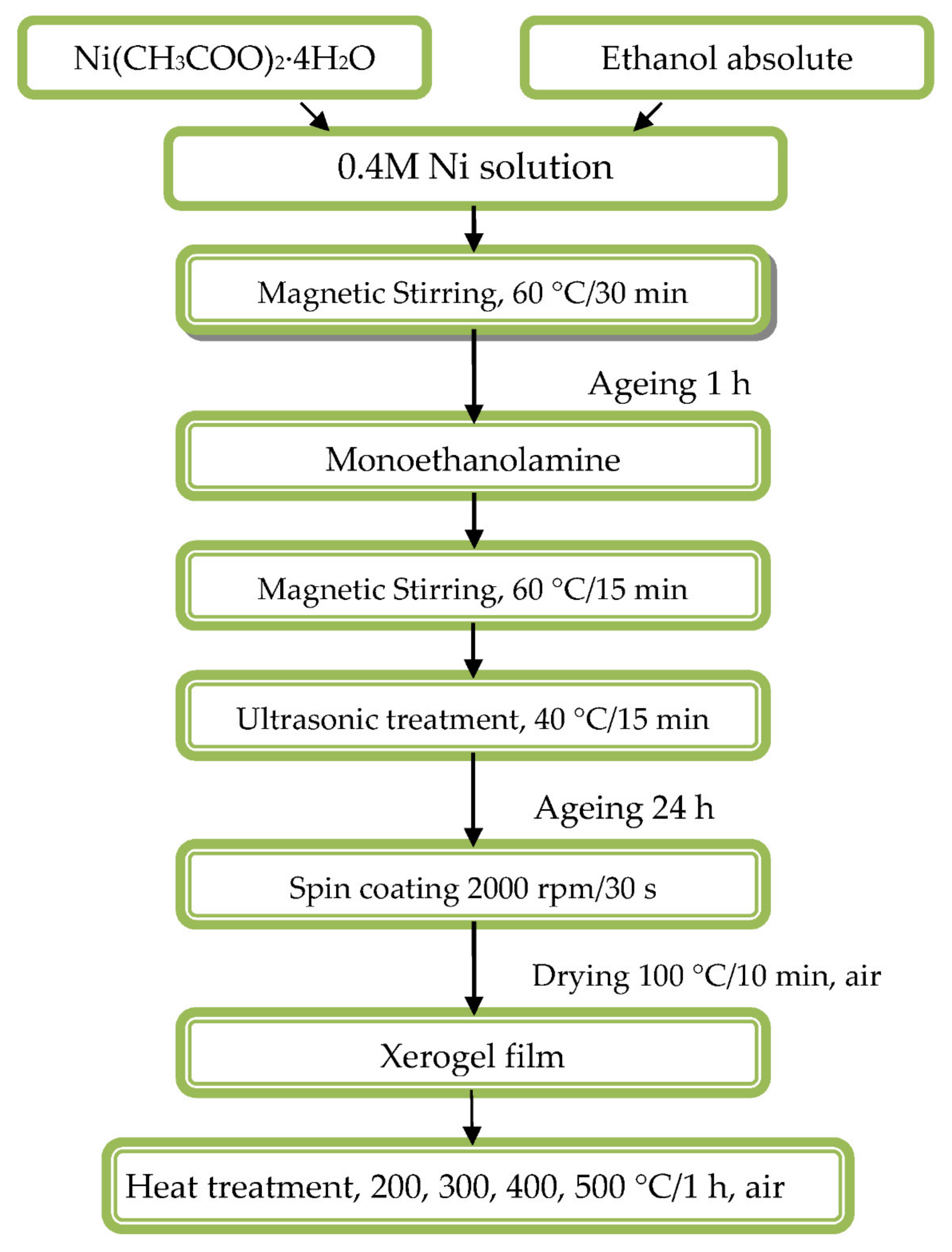
2.1. Thin Films Preparation

The sol solution synthesis and the thin film deposition is schemed in Figure 1. The sol solution for NiO film deposition was prepared from Ni acetate (Ni(CH3COO)2·4H2O) (Alfa Aesar, Karlsruhe, Germany, 98%+ pure) as precursor and dissolved in absolute ethanol (Merck, Darmsstadt, Germany, absolute for analysis) to reach 0.4 M concentration. The solution was stirred on a magnetic stirrer (type ARE, Velp Scientifica s.r.l., Usmate, Italy) at 60 °C for 30 min. Monoethanolamine (MEA, Fluka AG, Buch, Switzerland, 98%) was used as a complexing agent in order to prevent precipitation. The molar ratio MEA/Ni was fixed to 1. After adding MEA, the solution was treated again on a magnetic stirrer at 60 °C for 15 min. The solution was then ultrasonically (ultrasonic cleaner, UST 2.8-100, Siel Ltd., Gabrovo, Bulgaria) treated at 40 °C for 15 min. The sol solution had been aged for 24 h. The obtained Ni sol solution was found to be homogeneous and transparent without precipitations and with good film forming properties.
NiOx thin films were spin coated on preliminary cleaned substrates (Spin coater P 6708, PI-KEM Limited, Staffordshire, UK). The substrates used for structural and surface chemistry studies were silicon wafers (FZ, p-type, resistivity 4.5–7.5 Ω, orientation ˂100˃), and for optical characterization, glass substrates were used. The substrates were preliminarily cleaned in acetone in an ultrasonic bath at 45 °C, ultrasonically treated in ethanol (60 °C), and finally washed in distilled water. After the coating solution was dispensed onto the substrates, the substrates were centripetally accelerated to 2000 rpm and spun at this rotational speed for 30 s in ambient air. After the spinning process, the films were dried at 100 °C for 10 min in order to remove organic residuals (preheating temperature procedure). The high temperature annealings were performed at the temperatures of 200, 300, 400, and 500 °C for 1 h in air with controlled constant heating and cooling rates of 10 °C/min in a chamber furnace (Tokmet—TK Ltd., Varna, Bulgaria).

2.2. Thin Film Characterization

The thickness measurement of the films was provided by an MProbe spectroscopic reflectometer MProbe UV-VisSR system developed by Semiconsoft Inc. (Southborough, MA, USA). Spectroscopic reflectometry is a powerful technique that can be used for a wide range of applications to measure both thickness and optical constants. The spectroscopic reflectance method has a clear advantage of higher precision of thickness measurements (with the exception of very thin films). The NiOx/Si samples were measured using the MProbe UV-VIS MSP system. Mprobe precision is ˂0.01 nm. The fit procedure for determing refractive index is less than 1% accurate.
A Shimadzu FTIR Spectrophotometer IRPrestige-21 (Shimadzu, Japan) was used to perform the Fourier Transform Infrared Spectroscopy measurements in the spectral range 350–4000 cm−1 with a resolution of 4 cm−1. The bare Si wafer was used as background.
The film composition and electronic structure were investigated by X-ray photoelectron spectroscopy (XPS). The measurements were carried out on an AXIS Supra electron- spectrometer (Kratos Analytical Ltd., Manchester, UK) using achromatic AlKα radiation with a photon energy of 1486.6 eV and a charge neutralization system. The binding energies (BE) were determined with an accuracy of ±0.1 eV. The chemical composition in the depth of the films was determined by monitoring the areas and binding energies of C 1s, O 1s, and Ni 2p photoelectron peaks. Using the commercial data-processing software of Kratos Analytical Ltd., the concentrations of the different chemical elements (in atomic %) were calculated by normalizing the areas of the photoelectron peaks to their relative sensitivity factors.
Optical transmittance and reflectance spectra were carried out by a UV–VIS–NIR Shimadzu 3600 double-beam spectrophotometer (Shimadzu, Japan) in the spectral region of 240–1200 nm with a resolution of 0.1 nm. The transmittance was measured against air and the reflectance was measured by using the specular reflectance attachment (5° incidence angle) and an Al-coated mirror as reference. The transmittance and reflectance spectra of bare glass substrate are given as reference.
The work function (WF) of the samples was measured with a Scanning Kelvin Probe (SKP5050). The equipment and methodology are from KP Technology, Wick, Caithness, Scotland, UK. The Kelvin probe measures the contact potential difference between a sample and tip. The WF of the sample is calculated by determining the WF of the tip calibrated against a known surface. The sheet resistance of NiO films on glass substrate structures was measured by the four point probe method using a VEECO instrument, model FPP-100, Plainview, New York, USA.

3. Results and Discussions
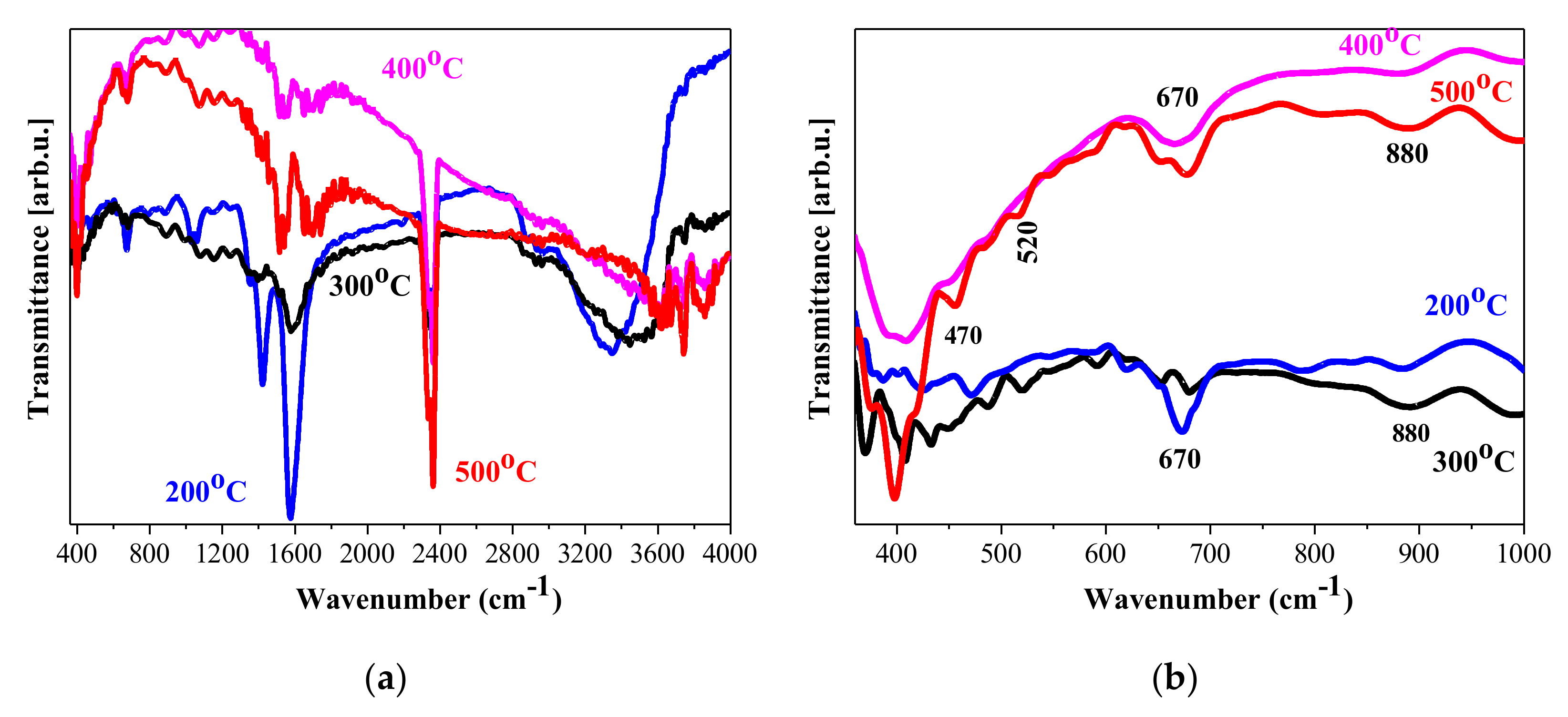
3.1. IR Study

IR spectroscopy is widely used for investigating sol-gel-derived films and the microstructural evolution with temperature and film processing parameters [25]. The FTIR spectra of NiO thin films are shown in Figure 2. The effect of annealing treatments on functional groups, vibrational modes, and the absorption band shapes and intensities was studied. It was seen that there are hydroxyl group vibrations that contribute to IR spectra and the corresponding absorption bands are changed with annealing. Generally, hydroxyl group stretching vibrations are mainly observed in the spectral range 3000–4000 cm−1 with the band at 1639 cm−1 attributed to the bending vibrations. The bands associated with the hydroxyl species are very strong and broad at lower annealing temperatures (200 and 300 °C), and they decrease in intensity with the increase of the temperatures to 400 and 500 °C.
The temperature treatment at 200 °C resulted in broad absorption bands centred at 3400 cm−1 for NiOx films (Figure 2a). The broad absorption, covering from 3000 to 3680 cm−1, clearly indicates contributions of different O-H stretching vibrations. The band at around 3400 cm−1 is attributed to interlayer water molecules and H-bound OH [26], at 3520–3566 cm−1 is associated with hydroxyl groups connected with Ni(OH)2 [27], and the band at 3634 cm−1 is characteristic for Ni(OH)2 [28]. The bending OH vibrations can be seen around 1600 cm−1. The weak lines at 886 cm−1 and at 680 cm−1 are related to bending modes of OH lattice in Ni(OH)2 [27] and wagging δOH vibrations, respectively [29]. These absorption features are observed in the spectra of the 300 °C sample with diminished intensities. NiOx films annealed at 400 and 500 °C manifest narrower and clear IR lines at 3615, 3750, and 3820 cm−1.
These lines are assigned to stretching vibrations of hydroxyl groups in free alignment [30] or due to Ni(OH)2 [27], interlayer water [31] and physisorbed H2O molecules, or terminal OH [32]. The peak at 880 cm−1 is changed, and at 675 cm−1, the line is shifted. IR lines at 2890, 2364, and 2334 cm−1 are due to C-H and to C-O (due to atmospheric CO2) vibrations [26], and respectively, the absorptions at 1420, 1350, 1065, and 1025 cm−1 are related to different C-H and C-O modes due to the deposition process [33]. The thermal treatments change the absorption bands due to hydroxyl groups, as the 3600 cm−1 band is shifted (300 °C) and vanished (for higher temperature annealed films).
The spectral range 350–650 cm−1 reveals many absorption lines attributed to Ni-O bonding vibrations. The line at 670 cm−1 (seen in all spectra, but very weak at higher temperatures) is related to hydroxyl groups in which H bonded to Ni-O [26]. This line suggests that adsorbed water is still present after annealing above 300 °C. The characteristic peaks of nanocrystalline NiO [34] are expressed at 445–540 cm−1, for all annealed films with the exception of NiOx, treated at 200 °C. The strong lines at 390–405 cm−1 (for films, treated at 300–500 °C) are assigned to transverse optical phonon frequency [35,36], observed in bulk NiO. The peaks at 470 and 520 cm−1 are due to Ni-O in cubic NiO [26] and to surface Ni-O [36], respectively. Interestingly, the lines at 380 and 460 cm−1 are associated with Ni(OH)2 [37], manifested in the spectra of NiOx films treated at 200 and 300 °C.
FTIR analysis revealed that hydroxyl species and IR absorptions due to Ni(OH)2 are seen in all spectra, but they are strongly influenced by the annealing temperatures. The IR lines due to hydroxyl group vibrations are significantly decreased, and mostly disappear with thermal treatment. The presence of Ni-O bonding is proved for NiOx films treated at temperatures 300–500 °C.

3.2. Chemical States of NiOx Thin Films

X-ray photoelectronic spectroscopy (XPS) is applied for revealing the chemical composition, defects states, and bonding states of Ni and O in the sol-gel NiO thin films. NiO is a transition metal oxide, and it is important to know the oxidation states. NiO exhibits spin–orbit doublet and its multiple peaks result in a complicated line shape, peak asymmetries, complex multiplet splitting, shake-up, plasmon loss structure, and overlapping binding energies, and it is difficult to determine the proportion of different Ni valences [38,39]. Figure 3 presents the XPS spectra of Ni 2p, O 1s, and C 1s core levels and their fitted results using Gaussian curves after the subtraction of a Shirley baseline.
XPS study revealed that there was a carbon contimination, monitored in the C 1s region. The deconvolution of C 1s spectra of 200 and 400 °C annealed samples consists of two peaks. The peak at 284.9 eV is usually related to C-C and the second peak at higher binding energy (BE) at 288.3 eV assigned to O-C=O [40]. The presence of carbon impurities is expected, as FTIR study shows the presence of carbon oxide residuals and adsorption from air.
The individual deconvoluted core level O 1s XPS spectra of NiOx films are presented in Figure 3b. The O 1s of NiOx film, annealed at 200 °C, is resolved into two well-pronounced peaks at the binding energies of 532.3 eV and 535.1 eV. This result is intriguing as it clearly asserts that there is no formation of a NiO phase at this annealing temperature. The main peak (532.3 eV) is mostly assigned to carbon contamination, H-O-H (adsorbed water) [40,41,42], or to the presence of NiO(OH) [43,44] (with the corresponding Ni 2p3/2 peak at 856.4 eV) (see Figure 3c). The 535.1 eV BE peak can be ascribed to water vapor in the film structure [45]. The existence of hydroxides and water inclusions is confirmed by FTIR spectroscopy and the corresponding expressed absorption bands. It should be noted that the chemical analysis showed that the oxygen concentration was very high, at. 74.8% for this sample (see Table 1).
The annealing at a higher temperature (400 °C) drastically changed the film microstructure. The O 1s spectrum revealed two definite lines. The first main peak is at the binding energy of 529.5 eV, due to metal-oxygen (O-Ni2+) bonds [46], and it is referred to as almost pure stoichiometric NiO [38]. The other peak, at BE = 531.3 eV, has been attributed to the formation of Ni2O3 (O -Ni3+) by many authors [41,44,46] (the corresponding Ni 2p3/2 peak at 855.7 eV is detected as can be observed in Figure 3c, but this can be disputed as it is also associated with adsorption of different oxygen-containing species such as Ni(OH)2 and NIO(OH), and defects in NiO [47,48]). In our study, the possible contributions both of Ni2O3 and hydroxyl species cannot be ruled out. IR absorptions due to Ni(OH)2 and water inclusions are manifested.
The obtained Ni 2p spectra contain two spin–orbit coupling spectra, Ni 2p3/2 and Ni 2p1/2 peaks. Both of them can be separated into four (200 °C) and five (400 °C) components using the Gaussian function (Figure 3c). Most researchers focus their XPS spectra interpretation on Ni 2p3/2 spectra. The first conclusion drawn from the Ni 2p spectra is that there is no appearance of metallic Nio (with main line at BE = 852.6 eV) [49].
The Ni 2p spectrum of NiOx film treated at 200 °C revealed two main peaks at 856.4 eV (Ni 2p3/2) and at 874.4 eV and two shake-up satellite peaks at 861.1 eV and 879.6 eV, respectively. As it has been discussed above, the peak at 856.4 eV is related to Ni3+ states in NiO(OH) [44], but other authors have assigned it to Ni2O3 (Ni3+) and to Ni(OH)2 (Ni2+) phases [46,50]. The probable existence of Ni hydroxides is supported by FTIR study and the positions of O 1s peaks.
The annealing at 400 °C leads to the appearance of a NiO phase as it has been seen from O 1s spectrum interpretation. The main peaks are located at 853.9 eV (Ni 2p3/2), 855.5 eV (Ni 2p3/2), and 872.8 eV (Ni 2p1/2). The first line, located at the binding energy of 853.9 eV, is attributed to Ni2+ states in NiO [40,42,50]. The Ni 2p3/2 at 853.9 eV and O 1s at 529.5 eV are reported to be due to Ni2+ states in Ni-O octahedrals in cubic NiO [43]. FTIR analysis revealed that the IR lines at 390–405, 470, and 520 cm−1 are due to Ni-O in cubic NiO for sol-gel NiOx films, treated at 400–500 °C.
The peak with BE = 855.5 eV corresponds to Ni3+ states either in Ni2O3 [51] or NiOOH [42,50], and their assignments can be confirmed by O 1s spectra at BE = 531.3 eV. It has been reported that Ni3+ states result from quasi-localized holes around Ni2+ vacancies in the lattice sites, and this results in an increase of p-type conductivity [43,52].
XPS analysis manifested that NiOx films annealed at the lowest annealing temperature may consist of Ni hydroxides, and the formation of the NiO phase was proved after 400 °C treatment. The presence of Ni3+ states was also found. These conclusions are supported by FTIR data.
It is known that in its stoichiometric form, NiO is an insulator. NiO material, obtained by different methods, is a metal-deficient p-type semiconductor; therefore, Ni vacancies are present at the cation lattice site [9]. Due to Ni vacancies, some Ni2+ ions must be converted to Ni3+ ions in order to maintain the electrical neutrality in the structure [9]. The Ni2+ deficiency, Ni3+ presence, and oxygen-rich nature directly contribute to the p-type conductivity of the NiOx film [53].

3.3. Thickness of the Films

The optical constants of NiOx thin films depend on stoichiometry, deposition method used, technological conditions, and film structure. Thus, in many cases, it is imperative to measure n and k simultaneously with the thickness to obtain accurate results. The NiOx/Si samples were measured using an MProbe UV-VisSR system in the 200–1000 nm wavelength range. NiOx dispersion was represented using the Exciton dispersion model, and T (transmittance), n (refractive index), and k (extinction) values were determined from the fit to the measured data. The results are presented in Table 2. A strong decrease of the film thickness was observed after thermal treatments. This can be due to significant densification for annealing temperatures above 200 °C. The hydroxyl groups and hydroxide and Nickel oxyhydroxide phases may exist in the film structure of 200 °C annealed samples, as has been deduced by IR and XPS measurements. Higher temperatures reduce these defects, and the NiO phase is formed.
The refractive index of bulk and stoichiometric NiO is 2.18 [54]. Generally, the crystalline material possesses a higher refractive index than the amorphous material. The values of measured refractive index for our sol-gel NiOx films are in agreement with the reported data [55,56].

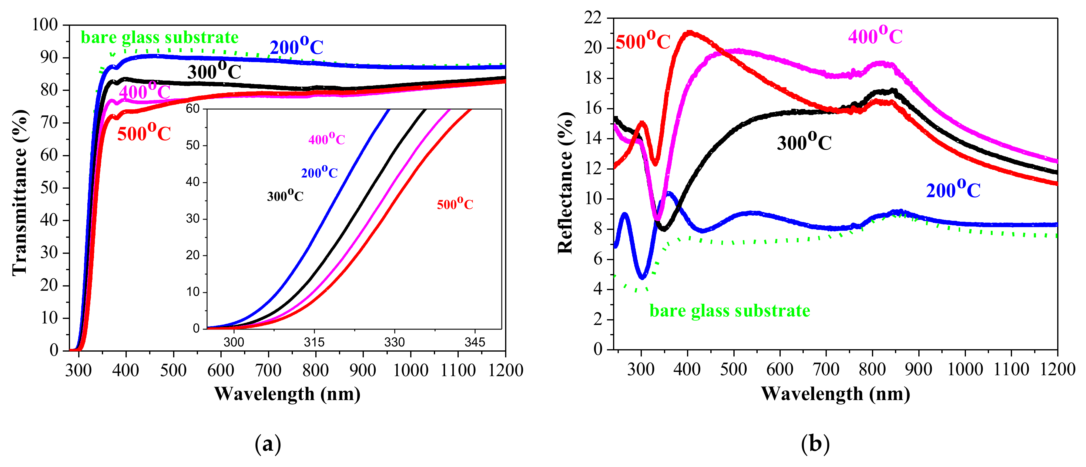
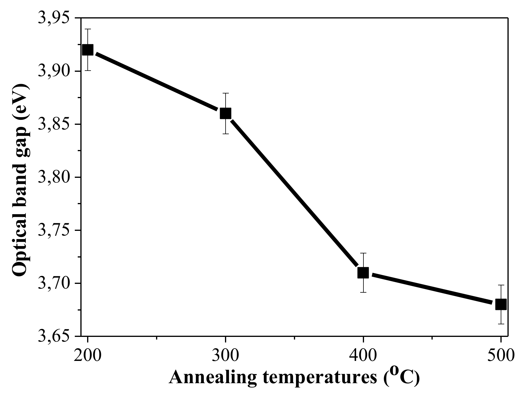
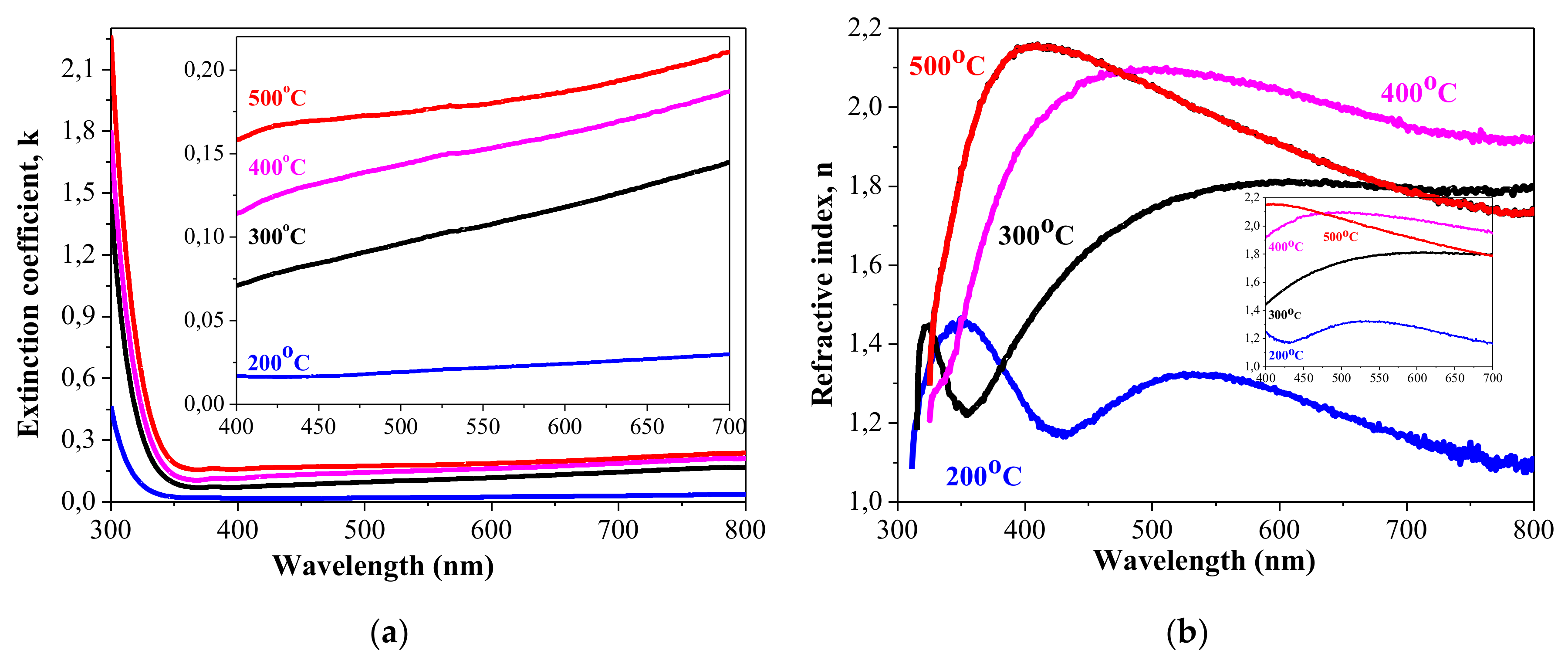
3.4. Optical Properties

Figure 4 shows the transmittance and reflectance spectra of NiOx film in the spectral range 240–1200 nm as a function of the annealing temperatures. The substrate used was glass. The transmittance in the wavelengths from 450 to 800 nm was affected by the annealings, as it dropped from almost 90% (200 °C sample) to 74–77% of 500 °C treated NiOx film. The reflectance reveals an increase from about 8% (200 °C) to about 20% (400 and 500 °C). It must be noted that the films cannot be directly compared due to significant differences in the film thickness of the 200 °C sample and the other NiOx films.
The lower transparency and higher reflectance of NiOx film annealed at temperatures above 200 °C can be due to structure modifications, crystallization, and rougher surfaces.
Figure 4 also manifests that the absorption edge of NiOx films is dependent on the thermal treatments, and it is red shifted. The optical band gap of sol-gel NiOx films is determined by Tuac’s plot, assuming direct transitions [1], namely the linear part of the (αhν)2 curve is extrapolated toward the energy axis at (αhν)2 = 0. The determined band gap values of NiOx films are in Figure 5 as a function of the annealing temperatures.
The obtained results clearly reveal that there is shrinkage of the optical band gap of NiOx films with increasing annealing temperatures. This can be due to the film crystallization, decreased defects of the films, and the increase of the crystallite sizes with the thermal treatments. Similar results have been reported in literature [1,10,40]. The decrease of the optical band gap and the shifting of the absorption edge to the higher wavelength with increasing annealing temperatures is reported for sol-gel NiO films [57]. This may be related to greater crystallites and decreased film porosity. The significantly smaller film thickness of the higher-temperature-treated NiOx can be due to film densification.
Figure 6 shows spectral dispersion of the optical constants of sol-gel NiOx films. The coefficient, k and refractive index, n of sol-gel NiOx films have been determined from the spectrophotometric data using the following relations [55,58]:
α = 1 d I n 1 T
k = α λ 4 π ,
n = 1 R 1 + R + 4 R 1 R 2 k 2 ,
where R is the film reflectance (substrate reflectance is subtracted), λ is the wavelength of the incident beam, and α is the absorption coefficient. The low values of extinction reveal the good transparency of the studied films. The extinction coefficient of 200 °C treated film is below 0.03 (400–700 nm). The extinction coefficient is higher for NiOx films treated at 300–500 °C, but their values are below 0.21 in the visible spectral range.
The refractive index is also dependent on the thermal treatments. It is known that the refractive index is higher for crystallized and denser samples than amorphous samples [58]. It can be seen that 200 °C film possess a refractive index of 1.24 at 630 nm and increases to 1.81 (300 °C), 2.02 (400 °C), and 1.86 (500 °C). There is a difference from the data given in Table 2, determined by spectral reflectometry. However, it must be pointed out that these values are measured of NiOx films on Si substrate. The determined refractive index of the 200 °C annealed sample is very low, but its structure is complicated, as shown by FTIR and XPS studies. It includes Ni hydrooxides and oxyhydroxides and is presumably amorphous. Other authors [58] also found closer refractive index values for amorphous sputtered NiO films. Table 3 presents the values of refractive index and optical band gap for NiO thin films, deposted by different technological methods.
The values of n in the range of 1.45–2.16 for NiOx films treated at 300, 400, and 500 °C and the optical band gap change (from 3.92 to 3.68 eV) coincide to the reported values as can be seen in Table 3 [54,59,60,61].

3.5. Electrical Characterization

We also determined the work function (WF) of NiOx thin films, which is an indicator of the quality and composition of the layers. The WF of NiOx thin films could be altered by different deposition techniques and the depositional parameters along with defects, such as oxygen vacancies or surface impurities, and composition [62]. It is reported that non-stoichiometric NiOx films with high Ni vacancies and additional oxygen have a WF larger than 5.0 eV [63]. The work function of NiO can be altered by exposing the sample to air and annealing to induce defects and remove excess oxygen. Table 4 shows that the work function changes slightly with increasing annealing temperature (with the exception of the sample annealed at 200 °C). In this case, the surface nickel hydroxide and adsorbed carbonaceous species affect the work function [64].
The sheet resistivity of NiOx films was measured by a four-point probe system, and the results are summarized along with annealing temperature in Table 5. The sheet resistivity of the NiOx films was measured on the insulating glass substrates. This corresponds to a resistivity of about 4.8 × 10⁻³ Ω·cm for NiOx film annealed at 400 °C. These values are significantly lower than those in [65,66,67].
Our results show that the samples after thermal treatment at 200 °C exhibit very low intrinsic conductivity. Increasing the temperature at and above 300 °C, NiOx manifests p-type conductivity. As it has been mentioned above, some authors [10,68] claim that NiOx is a metal-deficient p-type semiconductor and Ni vacancies are present at the cation lattice site, inducing the creation of Ni3+ ions. The metal vacancy and Ni3+ ions serve as hole acceptors, and this determines the p-type conductivity [69]. The presence of Ni3+ has been confirmed by XPS analysis for higher-temperature-treated NiOx films.

4. Conclusions

It has been demonstrated in this work that p-type conductive NiOx thin films of high quality can be deposited by the sol–gel technique using nickel acetate as a precursor instead of the usual alkoxides. The effect of the thermal treatments in the temperature range of 200–500 °C on the structural, optical, and electrical properties was studied. The main results can be summarized as follows:
  • XPS analysis showed that NiOx films annealed at the lowest annealing temperature may consist of Ni hydroxides and the formation of the NiO phase is proved after 400 °C treatment.
  • XPS analysis revealed that the higher annealing results in the cubic NiO phase (Ni2+ states) with presence Ni3+ states, which contribute to p-type conductivity of the films.
  • FTIR measurements also confirmed conclusions that the sol-gel NiOx film, annealed at 200 °C, consisted of other Ni oxide phases not cubic NiO with presence of hydroxyl and carbon species.
  • The transparency of NiOx films is high, with a slight decrease with annealing with an extinction coefficient below 0.03 (400–700 nm) of 200 °C annealed film and below 0.21 for NiOx films, treated at 300–500 °C in the visible spectral range. For NiOx film annealed at 200 °C, the refractive index is found to be in the range of 1.18–1.33. For NiOx film treated at 400 °C, it varies from 1.91–2.10. These values are determined for the spectral range 400–700 nm.
  • The optical band gap energy of sol–gel NiOx films decreases from 3.92 eV to 3.68 eV with increase in annealing temperature. These values coincide with the reported values for Ni oxide films.
  • NiOx thin films obtained by the sol-gel method are proven to possess p-type electrical conductivity. The 70-nm-thick layers have p-type conductivity and sheet resistance of 690 Ω/sq, which corresponds to a specific resistivity of about 4.8 × 10⁻³ Ω·cm. It was shown that at temperatures above 300 °C, NiOx thin films with good optical and electrical properties are obtained. Based on the research of the optical and electrical properties of NiOx, it was found that the quality of the NiOx films is comparable to that of films prepared by more complicated and expensive techniques such as rf magnetron sputtering, electron beam evaporation, MBE, etc.
  • The advantages of the sol-gel process are low cost, easy fabrication, long-term stability, and that they are suitable for use in large areas. The applied technological approach is compatible with that of deposition of zinc oxide, which implies successful integration of sol-gel processes for the realization of visible-light transparent solar cells.

Author Contributions

T.I.: Investigation, formal analysis; writing—original draft preparation, writing—review and editing; A.H.: Methodology, Investigation, Validation; M.S.: Investigation, formal analysis; P.V.: Conceptualization, writing—original draft preparation, Supervision. All authors have read and agreed to the published version of the manuscript.

Funding

This research received no external funding.

Institutional Review Board Statement

Not applicable.

Informed Consent Statement

Not applicable.

Data Availability Statement

The data are not publicly available.

Acknowledgments

The authors are kindly acknowledged for financial support to project No. BG05M2OP001-1.002-0014, Center of competence HITMOBIL—Technologies and systems for generation, storage and consumption of clean energy”, funded by Operational Programme “Science and Education For Smart Growth” 2014–2020, co-funded by the EU from European Regional Development Fund.

Conflicts of Interest

The authors declare no conflict of interest.

References

  1. Aftab, M.; Butt, M.Z.; Ali, D.; Bashir, F.; Khan, T.M. Optical and electrical properties of NiO and Cu-doped NiO thin films synthesized by spray pyrolysis. Opt. Mater. 2021, 119, 111369. [Google Scholar] [CrossRef]
  2. Gomaa, M.M.; Sayed, M.H.; Patil, V.L.; Boshta, M.; Patil, P.S. Gas sensing performance of sprayed NiO thin films toward NO2 gas. J. Alloys Compd. 2021, 885, 160908. [Google Scholar] [CrossRef]
  3. Kawade, D.; Chichibu, S.F.; Sugiyama, M. Experimental determination of band offsets of NiO-based thin film heterojunctions. J. Appl. Phys. 2014, 116, 163108. [Google Scholar] [CrossRef]
  4. Jin, S.; Wen, S.; Li, M.; Zhong, H.; Chen, Y.; Wang, X. Effect of the grain size on the electrochromic properties of NiO films. Opt. Mater. 2020, 109, 110280. [Google Scholar] [CrossRef]
  5. Faria, I.C.; Kleinke, M.; Gorenstein, A.; Fantini, M.C.A.; Tabacniks, M.H. Toward Efficient Electrochromic NiOx Films: A Study of Microstructure, Morphology, and Stoichiometry of Radio Frequency Sputtered Films. J. Electrochem. Soc. 1998, 145, 235–240. [Google Scholar] [CrossRef]
  6. Mihelcic, M.; Vuk, A.Š.; Jerman, I.; Orel, B.; Švegl, F.; Moulki, H.; Faure, C.; Campet, G.; Rougier, A. Comparison of electrochromic properties of Ni1−xO in lithium and lithium-free aprotic electrolytes: From Ni1−xO pigment coatings to flexible electrochromic devices. Sol. Energy Mater. Sol. Cells 2014, 120, 116–130. [Google Scholar] [CrossRef]
  7. Guo, X.; Wang, W.; Wen, R.-T. Enhanced electrochromic performance by anodic polarization in nickel oxide films. Crystals 2021, 11, 615. [Google Scholar] [CrossRef]
  8. Jabeen, S.; Iqbal, J.; Arshad, A.; Williams, J.; Samarin, S.; Rani, M. Heterojunction formation in In2O3–NiO nanocomposites: Towards high specific capacitance. J. Alloys Compd. 2020, 842, 155840. [Google Scholar] [CrossRef]
  9. Kim, S.K.; Seok, H.J.; Kim, D.H.; Choi, D.H.; Nam, S.J.; Kim, S.C.; Kim, H.K. Comparison of NiOx thin film deposited by spin-coating or thermal evaporation for application as a hole transport layer of perovskite solar cells. RSC Adv. 2020, 10, 43847–43852. [Google Scholar] [CrossRef]
  10. Kaya, D.; Aydınoğlu, H.S.; Tüzemen, E.Ş.; Ekicibile, A. Investigation of optical, electronic, and magnetic properties of p-type NiO thin film on different substrates. Thin Solid Films 2021, 732, 138800. [Google Scholar] [CrossRef]
  11. Sahoo, P.; Sharma, A.; Padhan, S.; Thangavel, R. Cu doped NiO thin film photocathodes for enhanced PEC performance. Superlattices Microstruct. 2021, 15, 107050. [Google Scholar] [CrossRef]
  12. Dawson, J.A.; Guo, Y.; Robertson, J. Energetics of intrinsic defects in NiO and the consequences for its resistive random access memory performance. Appl. Phys. Lett. 2015, 107, 122110. [Google Scholar] [CrossRef]
  13. Klochko, N.P.; Kopach, V.R.; Tyukhov, I.I.; Zhadan, D.O.; Klepikova, K.S.; Khrypunov, G.S.; Petrushenko, S.I.; Lyubov, V.M.; Kirichenko, M.V.; Dukarov, S.V.; et al. Metal oxide heterojunction (NiO/ZnO) prepared by low temperature solution growth for UV-photodetector and semi-transparent solar cell. Sol. Energy 2018, 164, 149–159. [Google Scholar] [CrossRef]
  14. Kumar, N.; Nguyen, T.T.; Park, H.-H.; Lee, K.; Kim, S.M.; Kim, J. Role of substrate architecture and modelling on photocurrent and photovoltage in TiO2/NiO transparent photovoltaic. Mater. Res. Bull. 2021, 142, 111421. [Google Scholar] [CrossRef]
  15. Nguyen, T.T.; Patel, M.; Kim, S.; Mir, R.A.; Yi, J.; Dao, V.-A.; Kim, J. Transparent photovoltaic cells and self-powered photodetectors by TiO2/NiO heterojunction. J. Power Sources 2021, 481, 228865. [Google Scholar] [CrossRef]
  16. Karsthof, R.; Racke, P.; von Wenckstern, H.; Grundmann, M. Semi-transparent NiO/ZnO UV photovoltaic cells. Phys. Status Solidi A 2016, 213, 30–37. [Google Scholar] [CrossRef]
  17. Weng, S.; Tamang, A.; Salleo, A.; Fujiwara, H.; Nakamura, M.; Zhang, Y.; Knip, D. Band-gap-engineered transparent perovskite solar modules to combine photovoltaics with photosynthesis. ACS Appl. Mater. Interfaces 2021, 13, 39230–39238. [Google Scholar] [CrossRef]
  18. Aivalioti, C.; Papadakis, A.; Manidakis, E.; Kayambaki, M.; Androulidaki, M.; Tsagaraki, K.; Pelekanos, N.T.; Stoumpos, C.; Modreanu, M.; Craciun, G. Transparent all-oxide hybrid NiO:N/TiO2 heterostructure for optoelectronic applications. Electronics 2021, 10, 988. [Google Scholar] [CrossRef]
  19. Bonomo, M. Synthesis and characterization of NiO nanostructures: A review. J. Nanopart. Res. 2018, 20, 222. [Google Scholar] [CrossRef]
  20. Napari, M.; Huq, T.N.; Hoye, R.L.Z.; MacManus-Driscoll, J.L. Nickel oxide thin films grown by chemical deposition techniques: Potential and challenges in next-generation rigid and flexible device applications. InfoMat 2021, 3, 536–576. [Google Scholar] [CrossRef]
  21. Chtouki, T.; El Mrabet, M.; Tarbi, A.; Goncharova, I.; Erguig, H. Comprehensive review of the morphological, linear and nonlinear optical characterization of spin-coated NiO thin films for optoelectronic applications. Opt. Mater. 2021, 118, 111294. [Google Scholar] [CrossRef]
  22. Arunodaya, J.; Sahoo, T. Effect of Li doping on conductivity and band gap of nickel oxide thin film deposited by spin coating technique. Mater. Res. Express 2019, 7, 016405. [Google Scholar]
  23. Patel, M.; Kim, H.-S.; Kim, J.; Yun, J.-H.; Kim, S.J.; Choi, E.H.; Park, H.H. Excitonic metal oxide heterojunction (NiO/ZnO) solar cells for all-transparent module integration. Sol. Energy Mater. Sol. Cells 2017, 170, 246–253. [Google Scholar] [CrossRef]
  24. Hu, Z.; Chen, D.; Yang, P.; Yang, L.; Qin, L.; Huang, Y.; Zhao, X. Sol-gel-processed yttrium-doped NiO as hole transport layer in inverted perovskite solar cells for enhanced performance. Appl. Surf. Sci. 2018, 441, 258–264. [Google Scholar] [CrossRef]
  25. Innocenzi, P. Infrared spectroscopy of sol–gel derived silica-based films. J. Non Cryst. Solids 2003, 6, 309–319. [Google Scholar] [CrossRef]
  26. Kalam, A.; Al-Shihri, A.S.; Al-Sehemi, A.G.; Awwad, N.S.; Du, G.; Ahmad, T. Effect of pH on solvothermal synthesis of β-Ni(OH)2 and NiO nano-architectures: Surface area studies, optical properties and adsorption studies. Superlattices Microstruct. 2013, 55, 83–97. [Google Scholar] [CrossRef]
  27. Kaspar, J.; Bazarjani, M.S.; Schitco, C.; Gurlo, A.; Graczyk-Zajac, M.; Riedel, R. Electrochemical study of NiO nanosheets: Toward the understanding of capacity fading. J. Mater. Sci. 2017, 52, 6498–6505. [Google Scholar] [CrossRef]
  28. El-Kemary, M.; Nagy, N.; El-Mehasse, I. Nickel oxide nanoparticles: Synthesis and spectral studies of interactions with glucose. Mater. Sci. Semicond. Process. 2013, 16, 1747–1752. [Google Scholar] [CrossRef]
  29. Adekunle, A.S.; Oyekunle, J.A.O.; Oluwafemi, O.S.; Joshua, A.O.; Makinde, A.O.; Aderemi, O.; Ogunfowokan, A.O.; Eleruja, M.A.; Ebenso, E.E. Comparative catalytic properties of Ni(OH)2 and NiO nanoparticles towards the degradation of nitrite (NO2-) and Nitric Oxide (NO). Int. J. Electrochem. Sci. 2014, 9, 3008–3021. [Google Scholar]
  30. Shruthi, B.; Madhu, B.J.; Bheema Raju, V.; Vynatheya, S.; Veena Devi, B.; Jayashree, G.V.; Ravikumar, C.R. Synthesis, spectroscopic analysis and electrochemical performance of modified OI-nickel hydroxide electrode with CuO. J. Sci. Adv. Mater. Dev. 2017, 2, 93–98. [Google Scholar]
  31. Govindarajan, B.; Palanimuthu, R.; Manikandan, K.M. Influence of Mg doping in magnetic properties of NiO nanoparticles and its electrical applications. J. Mater. Sci. Mater. Electron. 2019, 30, 6519–6527. [Google Scholar] [CrossRef]
  32. Shaid, M.S.H.M.; Zaini, M.A.A.; Nasri, N.S. Evaluation of methylene blue dye and phenol removal onto modified CO2-activated pyrolysis tyre powder. J. Clean. Prod. 2019, 223, 487–498. [Google Scholar] [CrossRef]
  33. Sun, D.; Zhang, J.; Ren, H.; Cui, Z.; Sun, D. Influence of OH and SO42− anions on morphologies of the nanosized nickel hydroxide. J. Phys. Chem. C 2010, 114, 12110–12116. [Google Scholar] [CrossRef]
  34. Ghalmi, Y.; Habelhames, F.; Sayah, A.; Bahloul, A.; Nessark, B.; Shalabi, M.; Nunzi, J.M. Capacitance performance of NiO thin films synthesized by direct and pulse potentiostatic methods. Ionics 2019, 25, 6025–6033. [Google Scholar] [CrossRef]
  35. Sharma, P.K.; Singh, M.K.; Sharma, G.D.; Agrawal, A. NiO nanoparticles: Facile route synthesis, characterization and potential towards third generation solar cell. Mater. Today Proc. 2021, 43, 3061–3065. [Google Scholar] [CrossRef]
  36. Biju, V.; Khadar, M.A. Fourier transform infrared spectroscopy study of nanostructured nickel oxide. Spectrochim. Acta A Mol. Biomol. Spectrosc. 2003, 59, 121–134. [Google Scholar] [CrossRef]
  37. Adekunle, A.S.; Hall, D.S.; Lockwood, D.J.; Bock, C.; MacDougall, B.R. Nickel hydroxides and related materials: A review of their structures, synthesis and properties. Proc. R. Soc. A 2015, 471, 20140792. [Google Scholar]
  38. Salunkhe, P.; Ali, A.V.M.; Kekuda, D. Structural, spectroscopic and electrical properties of dc magnetron sputtered NiO thin films and an insight into different defect states. Appl. Phys. A 2021, 127, 390. [Google Scholar] [CrossRef]
  39. Koshtyal, Y.; Nazarov, D.; Ezhov, I.; Mitrofanov, I.; Kim, A.; Rymyantsev, A.; Lyutakov, O.; Popovich, A.; Maximov, M. Atomic Layer Deposition of NiO to Produce Active Material for Thin-Film Lithium-Ion Batteries. Coatings 2019, 9, 301. [Google Scholar] [CrossRef] [Green Version]
  40. Chen, Z.; Dedova, T.; Asik, I.O.; Danilson, M.; Krunks, M. Nickel oxide films by chemical spray: Effect of deposition temperature and solvent type on structural, optical, and surface properties. Appl. Surf. Sci. 2021, 548, 149118. [Google Scholar] [CrossRef]
  41. Tran, M.H.; Park, B.J.; Yoon, H.H. A highly active Ni-based anode material for urea electrocatalysis by a modified sol–gel method. J. Colloid Interface Sci. 2020, 578, 641–649. [Google Scholar] [CrossRef] [PubMed]
  42. Acuña, J.R.A.; Perez, I.; Sosa, V.; Gamboa, F.; Elizalde, J.T.; Farías, R.; Carrillo, D.; Enríquez, J.L.; Burrola, A.; Mani, P. Sputtering power effects on the electrochromic properties of NiO films. Optik 2021, 231, 166509. [Google Scholar] [CrossRef]
  43. Seo, Y.-H.; Cho, I.H.; Na, S.-I. Investigation of sol-gel and nanoparticle-based NiOx hole transporting layer for high-performance planar perovskite solar cells. J. Alloys Comp. 2019, 797, 1018–1024. [Google Scholar] [CrossRef]
  44. Hu, H.; Zhu, J.; Chen, M.; Guo, T.; Li, F. Inkjet-printed p-type nickel oxide thin-film transistor. Appl. Surf. Sci. 2018, 441, 295–302. [Google Scholar] [CrossRef]
  45. Křepelová, A.; Newberg, J.; Huthwelker, T.; Bluhm, H.; Ammann, M. The nature of nitrate at the ice surface studied by XPS and NEXAFS. Phys. Chem. Chem. Phys. 2010, 12, 8870–8880. [Google Scholar] [CrossRef] [PubMed]
  46. Yu, J.-H.; Nam, S.-H.; Gil, Y.E.; Boo, J.-H. The effect of ammonia concentration on the microstructure and electrochemical properties of NiO nanoflakes array prepared by chemical bath deposition. Appl. Surf. Sci. 2020, 532, 147441. [Google Scholar] [CrossRef]
  47. Xu, X.; Zhang, H.; Tong, Y.; Sun, Y.; Fang, X.; Xu, J.; Wang, X. Tuning Ni3+ quantity of NiO via doping of cations with varied valence states: The key role of Ni3+ on the reactivity. Appl. Surf. Sci. 2021, 550, 149316. [Google Scholar] [CrossRef]
  48. Weidler, N.; Schuch, J.; Knaus, F.; Stenner, P.; Hoch, S.; Maljusch, A.; Schäfer, R.; Kaiser, B.; Jaegermann, W. X-ray Photoelectron Spectroscopic Investigation of Plasma-Enhanced Chemical Vapor Deposited NiOx, NiOx(OH)y, and CoNiOx(OH)y: Influence of the Chemical Composition on the Catalytic Activity for the Oxygen Evolution Reaction. J. Phys. Chem. C 2017, 121, 6455–6465. [Google Scholar] [CrossRef]
  49. Grosvenor, A.P.; Biesinger, M.C.; Smart, R.S.C.; McIntyre, N.S. New interpretations of XPS spectra of nickel metal and oxides. Surf. Sci. 2006, 600, 1771–1779. [Google Scholar] [CrossRef]
  50. Zhou, J.; Luo, G.; Wei, Y.; Zheng, J.; Xu, C. Enhanced electrochromic performances and cycle stability of NiO-based thin films via Li–Ti co-doping prepared by sol–gel method. Electrochim. Acta 2015, 186, 182–191. [Google Scholar] [CrossRef]
  51. Chia-Ching, W.; Cheng-Fu, Y. Investigation of the properties of nanostructured Li-doped NiO films using the modified spray pyrolysis method. Nanoscale Res. Lett. 2013, 8, 33. [Google Scholar] [CrossRef] [Green Version]
  52. Salunkhe, P.; Ali, M.A.V.; Kekuda, D. Investigation on tailoring physical properties of nickel oxide thin films grown by dc magnetron sputtering. Mater. Res. Express 2020, 7, 016427. [Google Scholar] [CrossRef]
  53. Kumar, N.; Lee, H.B.; Hwang, S.; Kang, J.W. Large-area, green solvent spray deposited nickel oxide films for scalable fabrication of triple-cation perovskite solar cells. J. Mater. Chem. A 2020, 8, 3357–3368. [Google Scholar] [CrossRef]
  54. Ukoba, K.O.; Eloka-Eboka, A.C.; Inambao, F.L. Review of nanostructured NiO thin film deposition using the spray pyrolysis technique. Renew. Sustain. Energy Rev. 2018, 82, 2900–2915. [Google Scholar] [CrossRef]
  55. Shkir, M.; Ganesh, V.; AlFaify, S.; Yahia, I.S.; Zahran, H.Y. Tailoring the linear and nonlinear optical properties of NiO thin films through Cr3+ doping. J. Mater. Sci. Mater. Electron. 2018, 29, 6446–6457. [Google Scholar] [CrossRef]
  56. Aydin, H.; Mansour, S.A.; Aydin, C.; Al-Ghamdi, A.A.; Al-Hartomy, O.A.; El-Tantawy, F.; Yakuphanoglu, F. Optical properties of nanostructure boron doped NiO thin films. J. Solgel Sci. Technol. 2012, 64, 728–733. [Google Scholar] [CrossRef]
  57. Nalage, S.R.; Chougule, M.A.; Sen, S.; Joshi, P.B.; Patil, V.B. Sol–gel synthesis of nickel oxide thin films and their characterization. Thin Solid Films 2012, 520, 4835–4840. [Google Scholar] [CrossRef]
  58. Usha, K.S.; Sivakumar, R.; Sanjeeviraja, C. Optical constants and dispersion energy parameters of NiO thin films prepared by radio frequency magnetron sputtering technique. J. Appl. Phys. 2013, 114, 123501. [Google Scholar] [CrossRef]
  59. Emam-Ismail, M.; El-Hagary, M.; El-Sherif, H.M.; El-Naggar, A.M.; El-Nahass, M.M. Spectroscopic ellipsometry and morphological studies of nanocrystalline NiO and NiO/ITO thin films deposited by e-beams technique. Opt. Mater. 2021, 112, 110763. [Google Scholar] [CrossRef]
  60. Mahmoud, S.A.; Alshomer, S.; Tarawnh, M.A. Structural and optical dispersion characterization of sprayed nickel oxide thin films. J. Modern Phys. 2011, 2, 1178–1186. [Google Scholar] [CrossRef] [Green Version]
  61. Rashad, M.; Darwish, A.A.A.; Qashou, S.I.; Abd El-Rahman, K.F. Influence of ultraviolet irradiation on physical properties of nano-NiO films for optical applications. Appl. Phys. A 2020, 126, 862. [Google Scholar] [CrossRef]
  62. Dutta, T.; Gupta, P.; Gupta, A.; Titas, J.N. High work function (p-type NiO1+ x)/Zn0. 95Ga0.05O heterostructures for transparent conducting oxides. J. Phys. D Appl. Phys. 2010, 43, 105301. [Google Scholar] [CrossRef]
  63. Yip, H.L.; Jen, A.K.-Y. Recent advances in solution-processed interfacialmaterials for efficient and stable polymer solar cells. Energy Environ. Sci. 2012, 5, 5994–6011. [Google Scholar] [CrossRef]
  64. Greiner, M.T.; Helander, M.G.; Wang, Z.-B.; Tang, W.-M.; Lu, Z.-H. Effects of processing conditions on the work function and energy-level alignment of NiO thin films. J. Phys. Chem. C 2010, 114, 19777–19781. [Google Scholar] [CrossRef]
  65. Tyagi, M.; Tomar, M.; Gupta, V. Post deposition annealing of NiOx thin films: A transition from n-type to p-type conductivity for short wave length optoelectronic devices. J. Mater. Res. 2013, 28, 723–732. [Google Scholar] [CrossRef]
  66. Jlassi, M.; Sta, I.; Hajji, M.; Ezzaouia, H. Optical and electrical properties of nickel oxide thin films synthesized by sol–gel spin coating. Mater. Sci. Semicond. Process. 2014, 21, 7–13. [Google Scholar] [CrossRef]
  67. Menchini, F.; Grilli, M.L.; Dikonimos, T.; Mittiga, A.; Serenelli, L.; Salza, E.; Chierchia, R.; Tucci, M. Application of NiOx thin films as p-type emitter layer in heterojunction solar cells. Phys. Status Solidi C 2016, 13, 1006–1010. [Google Scholar] [CrossRef]
  68. Kim, D.S.; Lee, H.C. Nickel vacancy behavior in the electrical conductance of nonstoichiometric nickel oxide film. J. Appl. Phys. 2012, 112, 034504. [Google Scholar] [CrossRef]
  69. Jang, W.L.; Lu, Y.M.; Hwang, W.S.; Hsiung, T.L.; Wang, H.P. Point defects in sputtered NiO films. Appl. Phys. Lett. 2009, 94, 062103. [Google Scholar] [CrossRef]
Figure 1. Scheme of the sol solution preparation and technological sequence of NiOx film deposition.
Materials 15 01742 g001
Figure 2. (a) FTIR spectra of sol-gel NiOx films treated at 200 °C, 300 °C, 400 °C, and 500 °C; (b) presents FTIR spectra in the shorter spectral range 350 - 1000 cm-1.
Materials 15 01742 g002
Figure 3. XPS spectra of (a) C 1s, (b) O 1s, and (c) Ni 2p core levels of NiOx films, 1 layer, treated at 200 °C and 400 °C.
Materials 15 01742 g003
Figure 4. (a) Transmittance spectra of NiOx films, annealed at the temperatures of 200, 300, 400, and 500 °C. The inset figure presents the absorption edges of NiOx films. (b) Corresponding reflectance spectra.
Materials 15 01742 g004
Figure 5. Estimated optical band gap values of sol-gel NiOx films depending on the annealing temperatures from 200 to 500 °C.
Materials 15 01742 g005
Figure 6. Extinction coefficient (a) and refractive index (b) of sol-gel NiOx films.
Materials 15 01742 g006
Table 1. The surface chemical composition of the sol-gel NiOx films.
ComponentAtomic %Mass Conc. %Ni/O Atomic %
NiOx films, annealed at 200 °C
O 1s74.848.30.27
Ni 2p20.047.4
NiOx films, annealed at 400 °C
O 1s56.426.10.76
Ni 2p42.972.9
Table 2. Film thickness and refractive index determined at the wavelength of 630 nm for sol-gel NiOx films. The NiOx/Si samples were measured using an Mprobe UV-VIS MSP system with precision <0.01 nm. The fit procedure for determing refractive index is less than 1% accurate.
Annealing Temperature [°C]Film Thickness [nm]Refractive Index
NiOx/Si, Reflectometry
Refractive Index
NiOx/Glass,
from R, T Data
2002131.551.24
300811.861.81
400731.902.02
500621.901.86
Table 3. The optical band gap and refractive index values of NiO films, deposited by various methods.
Optical Band Gap [eV]Refractive IndexSpectral RangeDeposition MethodReference
3.5722.15Average, 280–900 nmSpray pyrolisis[1]
3.63--Thermal evaporation[10]
3.40 (aqueous solution)Chemical spray[40]
4.00 (alcoholic solution)
3.25–4.001.871550 nmSpray pyrolisis[54] review
3.78–3.85˃2450–800 nmSol-gel[55]
3.731.82–1.42300–800 nmSol-gel[56]
3.47–3.86Decrease with annealingSol-gel[57]
3.12–3.932.0–1.4300–1000 nmMagnetron sputtering[58]
3.9542.2–1.9400–1000 nmE-beam technique[59]
3.14, 3.832.8–1.8300–1000 nmSpray pyrolisis[60]
3.50–3.812.10–1.45300–1000 nmWet method[61]
Table 4. Work Functions of sol-gel NiOx films, treated at different annealing temperatures.
Annealing Temperature [°C]Workfunction [eV]
2004.44
3005.29
4005.25
5005.24
Table 5. Sheet resistance values of sol-gel NiOx films treated at temperatures from 200 to 500 °C.
Annealing Temperature [°C]Sheet Resistance [Ω/sq]
200-
300689
400690
500689
Publisher’s Note: MDPI stays neutral with regard to jurisdictional claims in published maps and institutional affiliations.

