Article

First-Principles Study of Electronic Properties of Substitutionally Doped Monolayer SnP3

1
College of Science, University of Shanghai for Science and Technology, Shanghai 200093, China
2
School of Physics, Northeast Normal University, Changchun 130024, China
*
Author to whom correspondence should be addressed.
These authors contributed equally to this work.
Materials 2022, 15(7), 2462; https://doi.org/10.3390/ma15072462
Submission received: 9 March 2022 / Revised: 24 March 2022 / Accepted: 25 March 2022 / Published: 27 March 2022
(This article belongs to the Topic First-Principles Simulation—Nano-Theory)

Abstract

:
SnP3 has a great prospect in electronic and thermoelectric device applications due to its moderate band gap, high carrier mobility, absorption coefficients, and dynamical and chemical stability. Doping in two-dimensional semiconductors is likely to display various anomalous behaviors when compared to doping in bulk semiconductors due to the significant electron confinement effect. By introducing foreign atoms from group III to VI, we can successfully modify the electronic properties of two-dimensional SnP3. The interaction mechanism between the dopants and atoms nearby is also different from the type of doped atom. Both Sn7BP24 and Sn7NP24 systems are indirect bandgap semiconductors, while the Sn7AlP24, Sn7GaP24, Sn7PP24, and Sn7AsP24 systems are metallic due to the contribution of doped atoms intersecting the Fermi level. For all substitutionally doped 2D SnP3 systems considered here, all metallic systems are nonmagnetic states. In addition, monolayer Sn7XP24 and Sn8P23Y may have long-range and local magnetic moments, respectively, because of the degree of hybridization between the dopant and its adjacent atoms. The results complement theoretical knowledge and reveal prospective applications of SnP3-based electrical nanodevices for the future.

1. Introduction

In 2004, single-atom-thick sheets of graphene were successfully prepared by mechanical stripping [1]. Since then, two-dimensional materials have attracted much attention because of their intrinsic excellent physical and chemical characteristics [2,3,4,5,6,7,8,9,10,11,12,13]. The exploration of the ultra-thin two-dimensional system is also inspired by the latest experimental progress of controlled fabrication of nanomaterials. However, monolayer 2D materials are always limited by their inherent electronic properties. For example, the zero band gap of graphene restricts it from being used in practical electrical devices [3]. For 2D MoS2 with the direct band gap of 1.79 eV, abundant internal defects seriously reduce the mobility of carriers [4,14]. On the other hand, the boron nitride monomolecule is not an ideal candidate material for optoelectronic components or electronic devices because of its wide band gap. Therefore, it is significant to find an effective solution to improve their electronic properties. To further improve the performance of 2D materials, there are many methods such as adsorption, doping, and constructing heterogeneous junctions by stacking different materials, which have shown excellent effects in different fields [15,16]. In this research, doping is used to improve the performance of SnP3, which has been demonstrated as an effective and simple approach to modify the magnetic and electrical characteristics of 2D materials [5,6,7,8,9,17,18,19]. By doping heteroatoms, carbon-based materials exhibit exceptional electrochemical properties in lithium-ion and sodium-ion batteries [20]. Atomic metal ion-doped graphene offers strong conductivity and stability to the materials, resulting in good pseudocapacitance performance [21]. By inserting small BN domains, the band gap of graphene could well be efficiently expanded near K as well as K′ points [7]. MoS2 is usually stated as natively n-type while dopants quench the n-type, allowing it to perform as a single-photon emitter [22]. Doping various elements with even or odd amounts of valence electrons causes an oscillating behavior in black phosphorene [23].
Very recently, a 2D monolayer SnP3, one of the representative layered group-IV-based triphosphide family materials, has been theoretically proposed by Sun et al. [24]. The cleavage energy of monolayer SnP3 [24] is close to the cleavage energy of graphene. The cleavage energy of monolayer SnP3 [22] is comparable to that of graphene [25]. In its monolayer form, SnP3 exhibits semiconducting behavior, with the indirect bandgap determined as 0.42 eV by the PBE function [26] and 0.72 eV by the HSE06 function [27]. Furthermore, with a higher affinity to the NH3, NO, and NO2, the SnP3 monolayer has been described as a promising sensing material for tiny gas molecules [28,29]. Because of its high areal capacity and good stability, SnP3 is also widely employed in Na- and Li-ion batteries [30,31]. SnP3 has also been predicted with a high light absorption coefficient and carrier mobility [32] and has been found as an excellent p-type thermoelectric material [33]. With ultra-low thermal conductivity and high thermoelectric performance, monolayer SnP3 is considered as the potential candidate for thermoelectric materials [34]. The thermoelectric effect, as an essential part of the solution to today’s energy challenges, by reducing adverse effects on the environment, makes the application of SnP3 more extensive [35].
We have performed systematic investigations of the substitutionally doped SnP3 monolayer. The structural characteristics (including the optimized geometries, lattice constants, distortion) and electronic properties (including the energy band structures, density of states, and the charge densities) are systematically discussed. The doping atoms replaced Sn, including group III (B, Al, Ga) and group V (N, P, As), while dopants substituted for P are from group IV (C, Si, Ge) and group VI (O, S, Se). The electronic properties of doped 2D systems are strongly affected by the number of outer electrons in the dopants and the doping sites. Since each layer of bulk SnP3 is mainly connected by weak van der Waals forces, our study has guiding significance for understanding bulk SnP3 and also provides direction for future SnP3-based nanoscale applications.

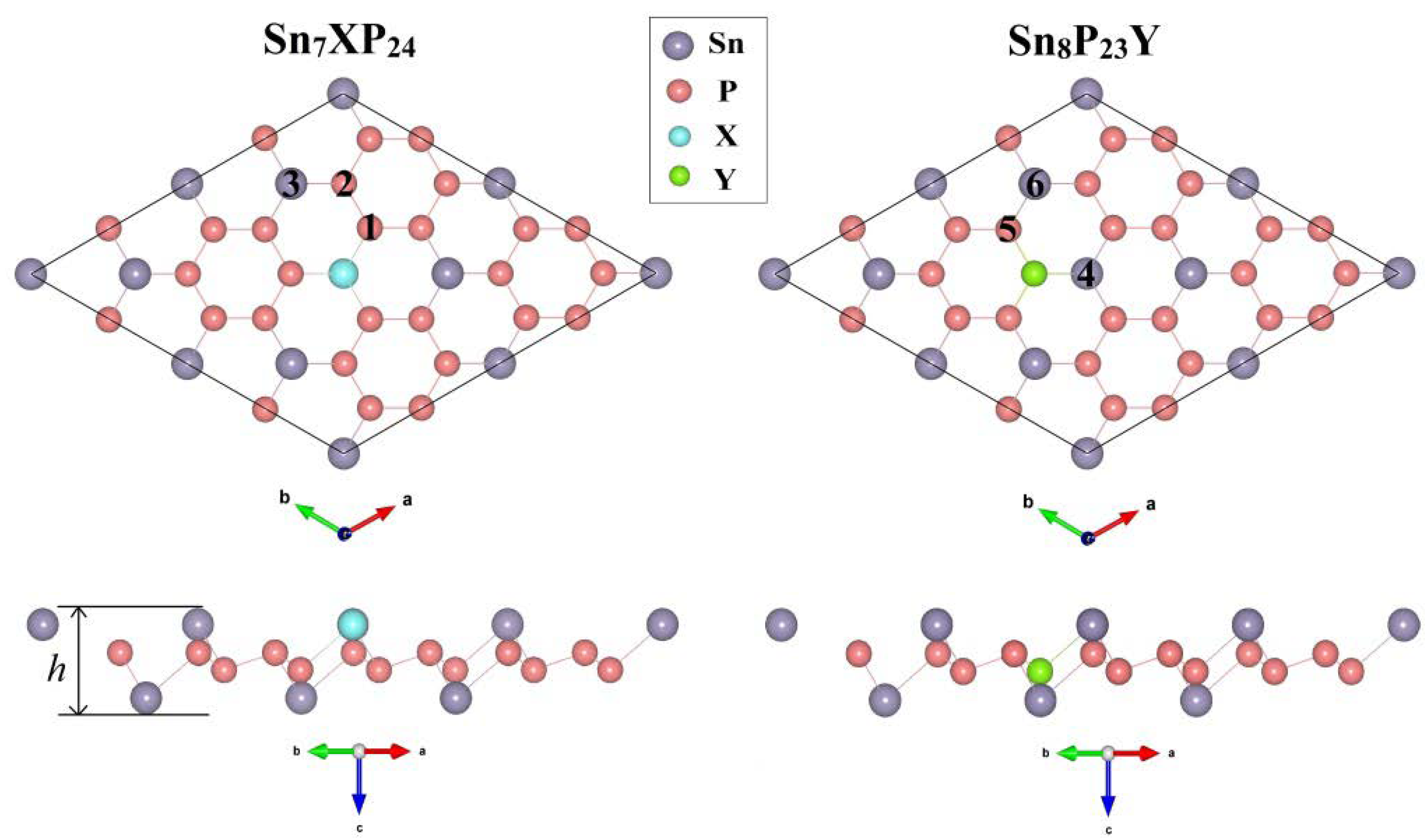
2. Computational Details

The Vienna ab initio simulation software (VASP) is performed to do the first principle calculations, which are based on the functional theory (DFT) of plane wave density and the projector augmented wave (PAW) approach [36,37]. In the Perdew-Burke-Ernzerhof (PBE) parameterization, the generalized gradient approximation (GGA) was used to describe the exchange-correlation interactions [38]. PBE functionals are related to semi-local functionals where the exchange-correlation energy is given by a function that depends on the electron density and the derivative of the electron density at each point of space. At the same time, SnP3 material is a layered structure with van der Waals (vdW)forces binding between layers. Since the DFT-GGA calculation lacks a prediction of the interlayer spacing of layer structures, we also take the van der Waals interaction (vdW) into consideration [39] by inserting a semi-empirical dispersion potential to the usual Kohn-Sham DFT energy (PBE-D2 computations). The plane wave function is used to create the electronic wave function, and the Monkhorst–Pack unique K-point sampling method is used to integrate the Brillouin zone (BZ) [40]. The vdW-D2 correction by Grimme is used to describe the interaction between SnP3 and dopant atoms over large distances. To eliminate the artificial contact between the neighboring periodic sheets, a 2 × 2 × 1 supercell with a vacuum layer of 20 Å in ‘z’ axis is utilized. A total of 500 eV was set as cut-off energy of the plane wave expansion. The Brillouin zone sampling was carried out using a 13 × 13 × 1 Γ-centered Monkhorst–Pack K-point mesh. All structures were completely relaxed until the total change in energy between two self-consistent steps was smaller than 1×10⁻⁴ eV.

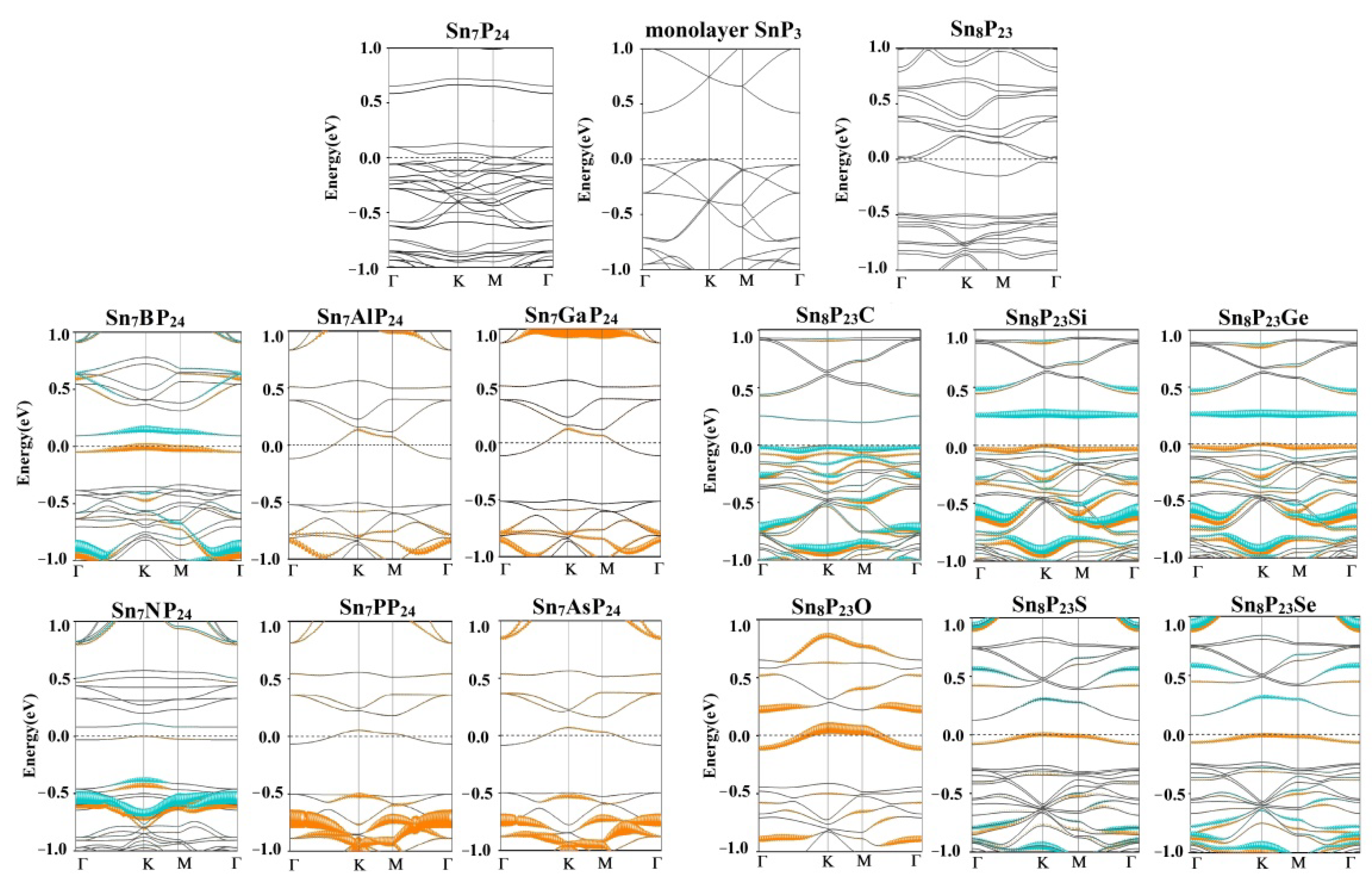
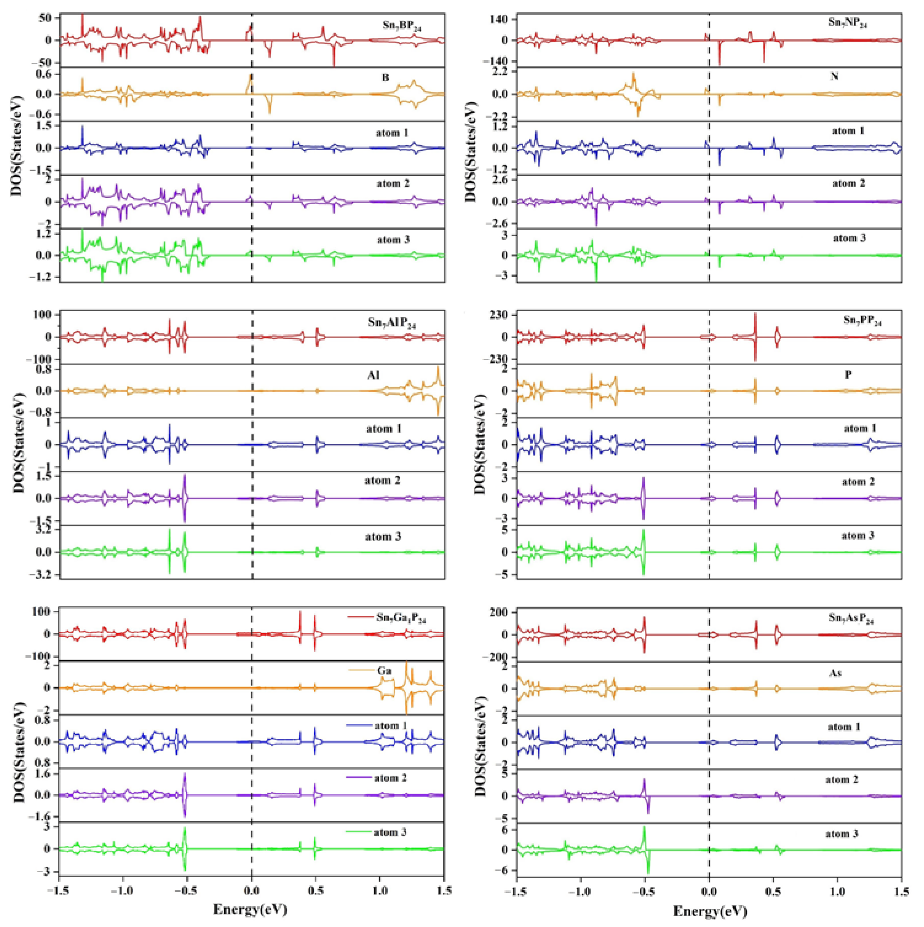
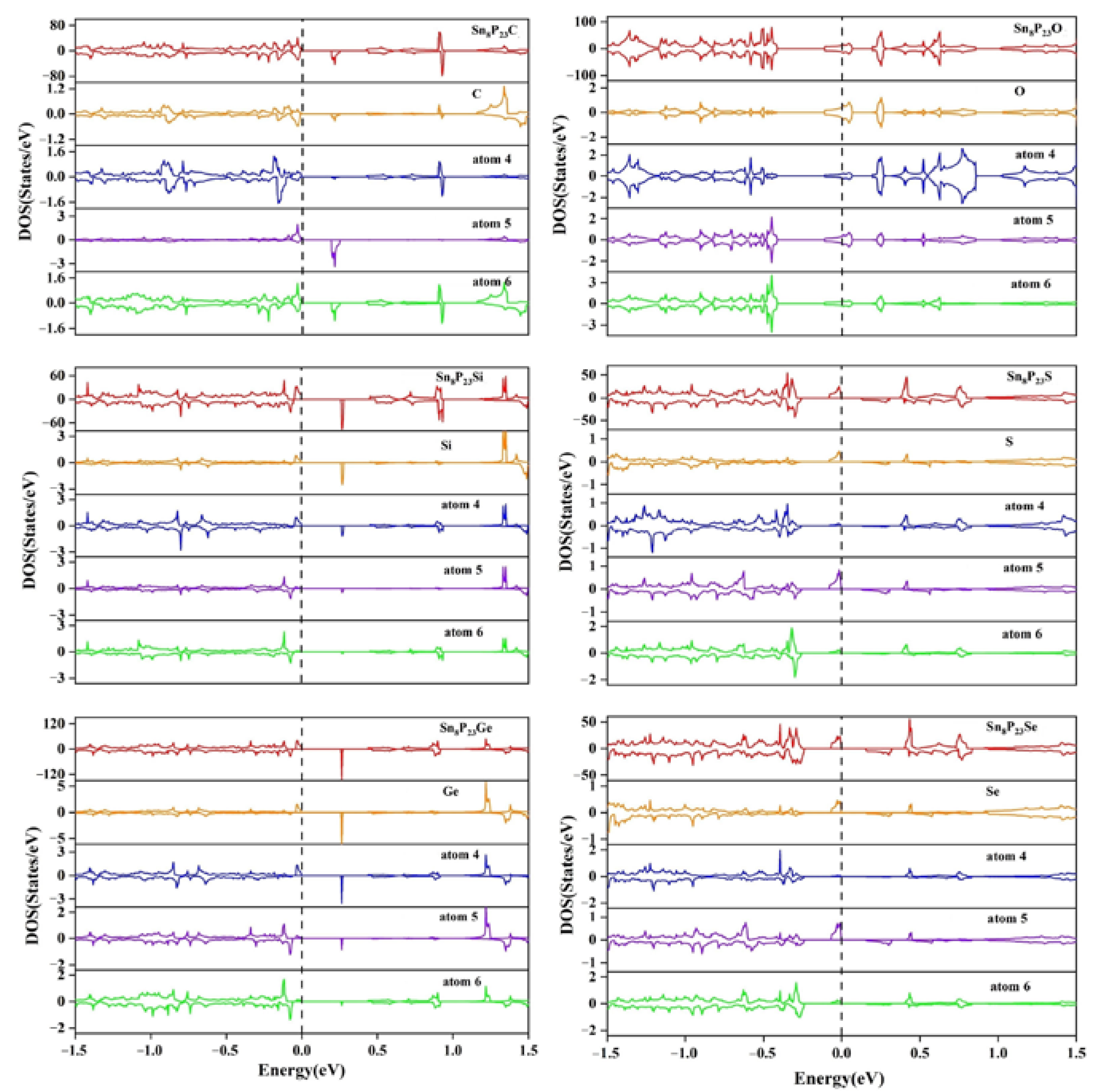
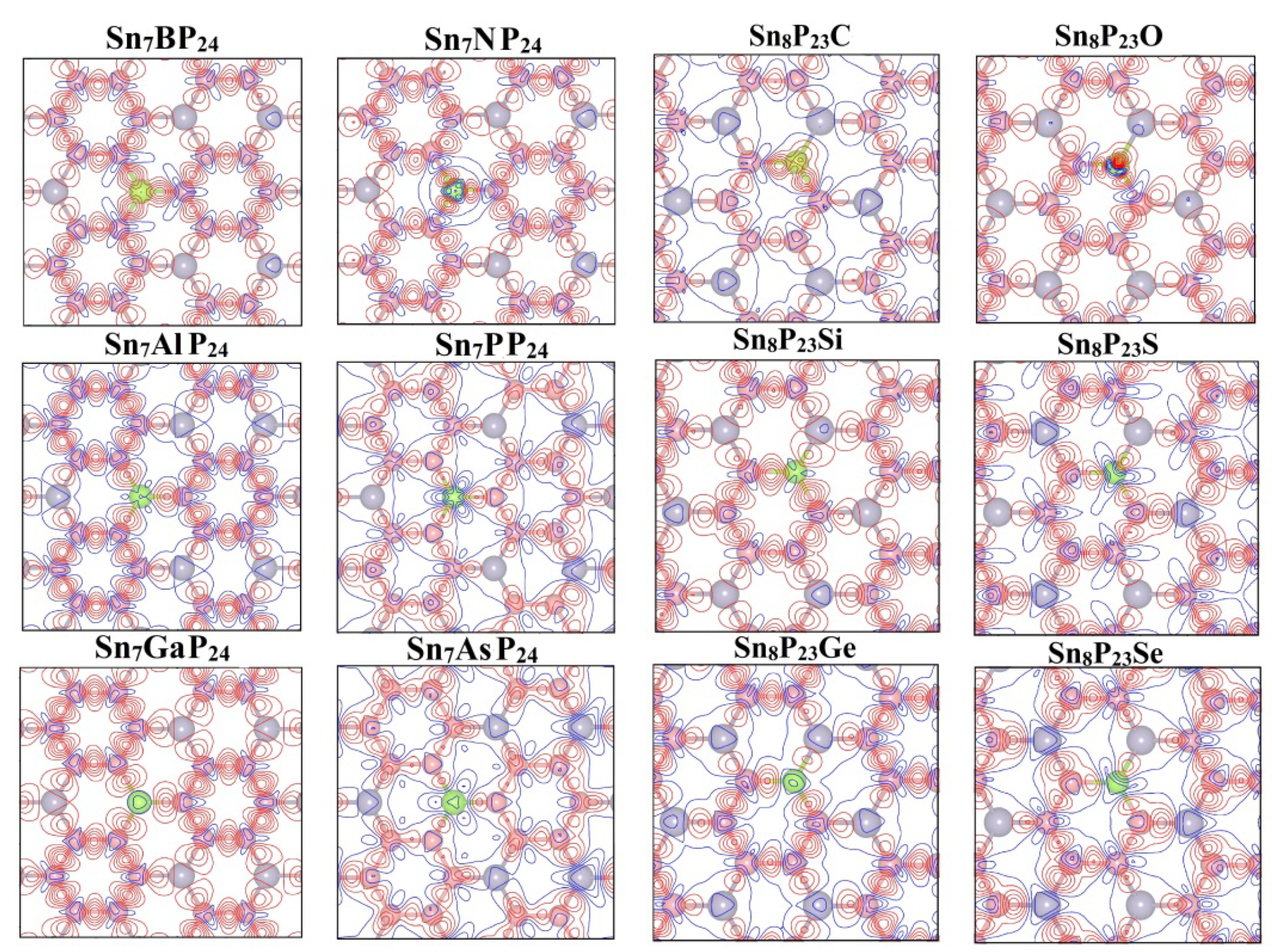
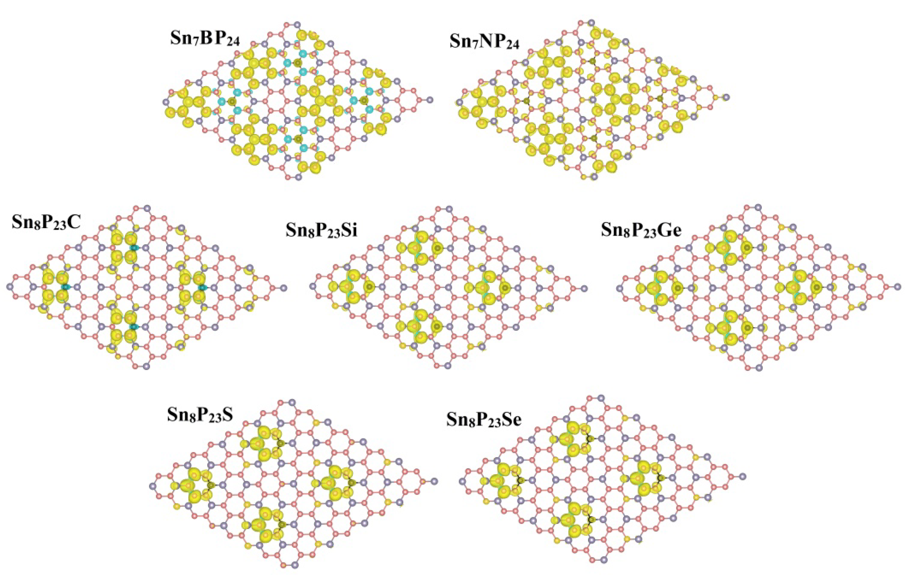
3. Result and Discussion

We established a 1 × 1 SnP3 cell (contains eight atoms) to determine the basic structural parameters of the 2D SnP3 system. After relaxation, the optimal lattice constant of the SnP3 supercell is 7.17 Å, which agrees well with the existing theoretical calculations [24,27,28]. The system was modeled based on a 2×2 SnP3 supercell (containing 32 atoms) for substitutionally doped SnP3 (shown in Figure 1) to minimize the influence of electrons states neighboring atoms. We first removed one Sn (or P) atom from the 2 × 2 SnP3 supercell and then replaced it with the one doped atom, which is labeled as X (or Y). The substitutionally doped SnP3 system is labeled as Sn7XP24 (or Sn8P23Y). Since the number of valence electrons in dopants has a great impact on the electronic characteristics of low dimensional materials, we select atom B, Al, and Ga from group III and atom N, P, As from group V as dopants for Sn atoms due to the one more or one less electron than Sn atoms. Similarly, we choose the atoms in group IV (C, Si, Ge), which has one less electron than P, and group VI (O, S, Se), which has one more electron as dopants for the P atom. The substitutional atoms are selected from the two adjacent groups of the Sn or P atom, each of which differs from the substituted atom by one outer electron.
After full relaxation, the lattice constant of 2 × 2 SnP3 is 14.32 Å. Table 1 displays the parameters of the Sn7XP24 and Sn8P23Y systems in which doped atoms have been replaced. We can see that the lattice constants of the doped systems are not much different from that before doping. Within the same group, the lattice constants rise as the atomic number increases. This is owed to the influence of the ionic radius’s effect upon the length of bonds. Although the insertion of doping atoms breaks the symmetry of the defect-free SnP3, the structure of the doping system typically retains the original hexagonal frame structure.
To evaluate the stability and feasibility of substitutionally doped SnP3 monolayer, the formation energy (Ef) of the system is given as follows:
E f = E t o t a l + E r e p l a c e d E p r i s t i n e E D
where E t o t a l   stands for the total energy of the SnP3 monolayer after doping (Sn7XP24 or Sn8P23Y). E p r i s t i n e denotes the total energy of the pure Sn8P24. The chemical potentials of single X (or Y) and Sn (or P) atoms are symbolized by E D and E r e p l a c e d , respectively. With the exception of Sn7BP24 and Sn8P23C, the formation energies of all of these doping systems are quite low. Particularly, the formation energies of Sn7BP24, Sn7PP24, Sn7AsP24, Sn8P23C, Sn8P23Si, and Sn8P23O systems are negative. The positive or negative formation energy can reflect the stability of the systems. The results implied that the substitutional doping processes of these systems are stable and exothermal. The lengths of bond P-X/P-Y and bond Sn-P/Sn-Y are listed in Table 1 to study the structural deformation in the Sn7XP24 or Sn8P23Y systems. In comparison to the length of the Sn-P bond (2.71 Å) in pristine monolayer SnP3, the d has pronounced change. Although the doped atoms from the same main group have similar electronic configurations, the larger ionic radius could promote sp3 hybridization. For the doped atoms in the same main group, the atomic radius increase with the atomic number. This would explain why P-X/P-Y and Sn-Y bond lengths increase as the number of protons increases. However, sheet thickness did not vary much because the configuration distortions generated by a single dopant atom are highly localized.
Figure 2 illustrates the substitutionally doped 2D SnP3 band structures obtained by the PBE-D2, the band gap values of different systems are shown in Table 1. The orange and blue dots represent the contributions of dopant atoms in spin-up and spin-down states, respectively. As presented in Figure 2, the pure SnP3 is a semiconductor with an indirect band gap of 0.42 eV, which agrees well with previous results [28,34,41]. The valence band maximum (VBM) is located at K-point, whereas the conduction band minimum (CBM) is found at Γ-point. When one Sn or P atom is removed from the 2 × 2 SnP3 monolayer, the system transforms into a metal. All B- and N-doped Sn7XP24 systems are indirect bandgap semiconductors. The band gaps of Sn7BP24 and Sn7NP24 are 0.08 and 0.09 eV, respectively. The band configurations of them are quite similar to the pristine monolayer SnP3. While the Sn7AlP24, Sn7GaP24, Sn7PP24, and Sn7AsP24 systems are metallic due to the contribution of doped atoms intersecting the Fermi level. This means the Al-, Ga-, P-, and As-doping of Sn atom in SnP3 could increase its conductivity. In the case of substitutional doping of the P atom in SnP3, however, only the Sn8P23O system appears to be metallic. For systems with dopants from group IV (C, Si, Ge) and group VI (S, Se), the doped Sn8P23Y systems could retain semiconducting properties. In our research, the contributions of dopants are mainly around the Fermi level. Thus, for all doped semiconductor systems, the addition of doped atoms reduces the band gap value. Compared with the P-vacancy system, the Fermi level moves up in Sn8P23O, Sn8P23S, and Sn8P23Se systems. Among Sn7XP24 systems, the doped atoms contribute significantly near the Fermi level for the magnetic Sn7BP24 and Sn7NP24 systems, while for Al-, Ga-, P- and As-doped systems, the dopants contribute more in deep level. Within each main group, the band gap value of the substitutionally doped SnP3 also increases with the increasing atomic number (shown in Table 1).
To illustrate the intrinsic mechanism of the substitutionally doped system, the densities of states of the substitutionally doped Sn7XP24 and Sn8P23Y systems are presented in Figure 3 and Figure 4, respectively. The partial density of states (PDOS) of the dopant atom and its adjacent atoms is also displayed in addition to the total density of states (TDOS). The locations of these atoms have been marked in Figure 1. As can be found in the PDOS, near the Fermi level, the impurity atom has a larger contribution to the doped system. For substitutional doping on the Sn site of SnP3 monolayer, only the Sn7BP24 and Sn7NP24 systems are semiconductors. We can see that the spin-up (fully occupied) and spin-down (unoccupied) states are totally different near the Fermi level. The unevenness occupation between spin-up and spin-down leads to magnetic moments in the doped system. However, among all considered Sn8P23Y systems, the occupation situations of the spin-up and spin-down states are very uneven except for Sn8P23O. For systems with unevenness DOS, the spin-up states are fully occupied, and spin-down states are unoccupied. For all Sn7XP24 systems considered here, no matter the SnP3 monolayer has magnetic moments or not, there is strong hybridization between the X atom and its nearest (atom 1) and second nearest neighbor (atom 2) P atoms. What is more, the same degrees of hybridization are found between the X atom and its third nearest Sn atoms (atom 3). This would lead to a long-range magnetic moment in the systems. However, for the substitutionally doped Sn8P23Y systems, there is only strong hybridization between the Y atom and its nearest (atom 4) Sn atoms. On the other hand, the Sn7AlP24, Sn7GaP24, Sn7PP24, and Sn7AsP24 systems are found to be metallic. Different from the substitutional doping on the Sn site, the semiconducting characteristics of the pure SnP3 monolayer are retained in the majority of Sn8P23Y systems. All group IV atoms-doped Sn8P23Y systems are semiconductors. The lowest unoccupied states fell below the Fermi level after substitutional doping of the O atom on the Sn site, showing n-type doping of the SnP3 monolayer.
To understand the mechanisms inherent in these low dimensional structures, which are necessary for the dynamics of material formation [42], the deformation charge density (Δρ) is also discussed in this work. The density of deformation charge is described as:
ρ ( r ) = ρ ( r ) μ ρ a t o m ( r R μ )
where the ρ ( r ) stands for the total charge density of the system and the μ ρ atom ( r R μ ) denotes the superposition of atomic charge densities. The extent of charge transfer between the dopant and the monolayer SnP3 could be measured through ρ ( r ) . The deformation charge density of planes slicing across the dopant atoms is shown in Figure 5. The electron accumulation ( ρ > 0 ) and electron depletion ( ρ < 0 ) are depicted by red and blue lines, respectively. For the Sn7BP24 and Sn7NP24 systems, there is obvious charge transfer from adjacent P atoms to dopant atoms. On the other hand, the electrons are apparently converging around the dopant atoms Sn8P23O and Sn8P23C systems. For doped atoms in the same main group, the properties of the bonds between dopant and its nearby atoms change with the atomic number of doped atoms. With the increase in dopants’ proton, the ionic component decreases, and the covalent component increases. At the same time, the electron transfer between atoms and the electron-accepting ability decreases as the atomic number increases. It can be explained by that electron-accepting ability decreases as the atomic number increases. Due to the strongest electron-accepting ability of the O atom, among all the substitutionally doped systems studied here, the most obvious electron transfer is found in the Sn8P23O system. Furthermore, when the covalent bonding ratio increases, the P-X and P-Y bond lengths of the substitutionally doped SnP3 monolayer also become longer. Thus, the distribution of electrons in the systems is significantly affected by the introduction of doping atoms.
For a long time, the magnetism of 2D materials has attracted a great deal of academic attention. The difference in charge density between the spin-up (ρ) and spin-down states (ρ) of substitutionally doped 2D SnP3 systems are presented in Figure 6. Table 1 also shows the total magnetic moments of the doped systems determined with PBE-D2. For substitutionally doped 2D SnP3 systems considered here, all metallic systems are nonmagnetic states. As mentioned above in Table 1, the magnetic moments of about 1.00 µB in doped systems were caused by the dopant atoms in the SnP3 monolayer. We found that the long-range magnetic moments can be found in the Sn7BP24 and Sn7NP24 systems, resulting from the strong hybridization between the B (or N) atom and its nearest P atoms, second nearest P atoms, and its third nearest Sn atoms. However, the magnetic Sn8P23Y (Y = C, Si, Ge, S, Se) systems only show local magnetic moments through the substitutional doping process. Thus, the 2D indirect bandgap SnP3 monolayer can attain local or long-range magnetic moments through the substitutional doping, resulting from the different interaction mechanisms between the doping atom and its neighboring atoms, which make the SnP3 sheet a promising material for nanoscale technological application in spintronic.

4. Conclusions

In summary, we investigated the electronic characteristics of substitutionally doped 2D SnP3 systems using first-principles calculations. One Sn atom is replaced with a dopant from group III (B, Al, Ga) and group V (N, P, As), while the P atom is replaced with an atom from group IV (C, Si, Ge) and group VI (O, S, Se). The substitutional atoms are selected from the two adjacent groups of the Sn or P atom due to one less or more electron. Our results show that the impurity atoms have a significant impact on the electronic characteristics of whole substitutionally doped systems. SnP3 monolayers can exhibit metallic or semiconducting behavior depending on the dopant type. All semiconductive systems are indirect band gap semiconductors with the introduced magnetic moments of about 1.00 µB. Within the same main group, the band gap and structural parameters increase as the atomic number of dopant rise. In addition, monolayer SnP3 may have local or long-range magnetic moments because of the degree of hybridization between the dopant and its adjacent atoms. This allows SnP3 monolayers to be widely used at the nanoscale in the field of spintronics. Since the doped atoms have a significant impact on the properties of the material, SnP3 is suitable for various functionalization processes.

Author Contributions

Conceptualization, N.Z.; Data curation, N.Z.; Formal analysis, S.L.; Investigation, N.Z., S.R. and T.H.; Methodology, X.C. and T.H.; Resources, X.L.; Supervision, X.L. All authors have read and agreed to the published version of the manuscript.

Funding

This research received no external funding.

Data Availability Statement

The data presented in this study are available on request from the corresponding author.

Conflicts of Interest

The authors declare no conflict of interest.

References

  1. Novoselov, K.S.; Geim, A.K.; Morozov, S.V.; Jiang, D.; Zhang, Y.; Dubonos, S.V.; Grigorieva, I.V.; Firsov, A.A. Electric Field Effect in Atomically Thin Carbon Films. Science 2004, 306, 666–669. [Google Scholar] [CrossRef] [PubMed] [Green Version]
  2. Geim, A.K.; Novoselov, K.S. The Rise of Graphene. Nat. Mater. 2007, 6, 183–191. [Google Scholar] [CrossRef] [PubMed]
  3. Novoselov, K.S.; Geim, A.K.; Morozov, S.V.; Jiang, D.; Katsnelson, M.I.; Grigorieva, I.V.; Dubonos, S.V.; Firsov, A.A. Two-Dimensional Gas of Massless Dirac Fermions in Graphene. Nature 2005, 438, 197–200. [Google Scholar] [CrossRef]
  4. Kadantsev, E.S.; Hawrylak, P. Electronic Structure of a Single MoS2 Monolayer. Solid State Commun. 2012, 152, 909–913. [Google Scholar] [CrossRef]
  5. Dong, X.; Shi, Y.; Zhao, Y.; Chen, D.; Ye, J.; Yao, Y.; Gao, F.; Ni, Z.; Yu, T.; Shen, Z.; et al. Symmetry Breaking of Graphene Monolayers by Molecular Decoration. Phys. Rev. Lett. 2009, 102, 135501. [Google Scholar] [CrossRef] [PubMed]
  6. Guzmán-Arellano, R.M.; Hernández-Nieves, A.D.; Balseiro, C.A.; Usaj, G. Diffusion of Fluorine Adatoms on Doped Graphene. Appl. Phys. Lett. 2014, 105, 026805. [Google Scholar] [CrossRef] [Green Version]
  7. Yousefi, M.; Faraji, M.; Asgari, R.; Moshfegh, A.Z. Effect of Boron and Phosphorus Co-doping on the Electronic and Optical Properties of Graphitic Carbon Nitride Monolayers: First-Principle Simulations. Phys. Rev. B 2018, 97, 195428. [Google Scholar] [CrossRef] [Green Version]
  8. Wang, Q.; Yu, W.; Fu, X.; Qiao, C.; Xia, C.; Jia, Y. Electronic and Magnetic Properties of SnSe Monolayers Doped by Ga, In, As, and Sb: A First-Principles Study. Phys. Chem. Chem. Phys. 2016, 18, 8158–8164. [Google Scholar] [CrossRef] [Green Version]
  9. Fan, X.; Shen, Z.; Liu, A.Q.; Kuo, J.L. Band gap opening of graphene by doping small boron nitride domains. Nanoscale 2012, 4, 2157–2165. [Google Scholar] [CrossRef]
  10. Shi, L.; Xu, A.; Zhao, T. First-Principles Investigations of the Working Mechanism of 2d h-Bn as an Interfacial Layer for the Anode of Lithium Metal Batteries. ACS Appl. Mater. Interfaces 2017, 9, 1987–1994. [Google Scholar] [CrossRef]
  11. Tongay, S.; Zhou, J.; Ataca, C.; Lo, K.; Matthews, T.S.; Li, J.; Grossman, J.C.; Wu, J. Thermally Driven Crossover from Indirect toward Direct Bandgap in 2D Semiconductors: MoSe2 versus MoS2. Nano Lett. 2012, 12, 5576–5580. [Google Scholar] [CrossRef] [PubMed]
  12. Zhou, Y.; Liu, G.; Zhu, X.; Guo, Y. Ultrasensitive NO2 Gas Sensing Based on RGO/MoS2 Nanocomposite Film at Low Temperature. Sens. Actuators B Chem. 2017, 251, 280–290. [Google Scholar] [CrossRef]
  13. Zhou, Y.; Zou, C.; Lin, X.; Guo, Y. UV Light Activated NO2 Gas Sensing Based on Au Nanoparticles Decorated Few-Layer MoS2 Thin Film at Room Temperature. Appl. Phys. Lett. 2018, 113, 082103. [Google Scholar] [CrossRef]
  14. Geng, X.; Zhang, Y.; Han, Y.; Li, J.; Yang, L.; Benamara, M.; Chen, L.; Zhu, H. Two-Dimensional Water-Coupled Metallic MoS2 with Nanochannels for Ultrafast Supercapacitors. Nano Lett. 2017, 17, 1825–1832. [Google Scholar] [CrossRef]
  15. Dastgeer, G.; Afzal, A.M.; Nazir, G.; Sarwar, N. p-GeSe/n-ReS2 Heterojunction Rectifier Exhibiting A Fast Photoresponse with Ultra-High Frequency-Switching Applications. Adv. Mater. Interfaces 2021, 8, 2100705. [Google Scholar] [CrossRef]
  16. Dastgeer, G.; Afzal, A.M.; Aziz, J.; Hussain, S.; Jaffery, S.H.A.; Kim, D.K.; Imran, M.; Assiri, M.A. Flexible Memory Device Composed of Metal-Oxide and Two-Dimensional Material (Sno2/WRe2) Exhibiting Stable Resistive Switching. Materials 2021, 14, 7535. [Google Scholar] [CrossRef] [PubMed]
  17. Li, H.; Zhang, L.; Cai, X.; Li, X.; Wang, B.; Yu, W.; Zhao, R. Metal-Nonmetal Oscillations in Doped Blue Phosphorene: A First-Principles Study. Mater. Res. Express. 2018, 5, 055007. [Google Scholar] [CrossRef]
  18. Liu, R.; Li, Y.; Yao, B.; Ding, Z.; Jiang, Y.; Meng, L.; Deng, R.; Zhang, L.; Zhang, Z.; Zhao, H.; et al. Shallow Acceptor State in Mg-Doped CuAlO2 and Its Effect on Electrical and Optical Properties: An Experimental and First-Principles Study. ACS Appl. Mater. Interfaces 2017, 9, 12608–12616. [Google Scholar] [CrossRef]
  19. Xie, H.-Q.; Zeng, Y.; Huang, W.-Q.; Peng, L.; Peng, P.; Wang, T.-H. First-Principles Study on Electronic and Optical Properties of La-Doped ZnS. Phys. B Condens. Matter. 2010, 405, 3899–3903. [Google Scholar] [CrossRef] [Green Version]
  20. Yuan, Y.; Chen, Z.; Yu, H.; Zhang, X.; Liu, T.; Xia, M.; Zheng, R.; Shui, M.; Shu, J. Heteroatom-Doped Carbon-Based Materials for Lithium and Sodium Ion Batteries. Energy Stor. Mater. 2020, 32, 65–90. [Google Scholar] [CrossRef]
  21. Liu, L.; Xie, Z.; Du, X.; Yu, D.; Yang, B.; Li, B.; Liu, X. Large-Scale Mechanical Preparation of Graphene Containing Nickel, Nitrogen and Oxygen Dopants as Supercapacitor Electrode Material. Chem. Eng. J. 2022, 430, 132515. [Google Scholar] [CrossRef]
  22. Tan, A.M.Z.; Freysoldt, C.; Hennig, R.G. First-Principles Investigation of Charged Dopants and Dopant-Vacancy Defect Complexes in Monolayer MoS2. Phys. Rev. Mater. 2020, 4, 114002. [Google Scholar] [CrossRef]
  23. Yu, W.; Zhu, Z.; Niu, C.Y.; Li, C.; Cho, J.H.; Jia, Y. Anomalous Doping Effect in Black Phosphorene Using First-Principles Calculations. Phys. Chem. Chem. Phys. 2015, 17, 16351–16358. [Google Scholar] [CrossRef] [PubMed] [Green Version]
  24. Sun, S.; Meng, F.; Wang, H.; Wang, H.; Ni, Y. Novel Two-Dimensional Semiconductor SnP3: High Stability, Tunable Bandgaps and High Carrier Mobility Explored Using First-Principles Calculations. J. Mater. Chem. A 2018, 6, 11890–11897. [Google Scholar] [CrossRef]
  25. Jin, Y.; Li, X.; Yang, J. Single Layer of MX3 (M = Ti, Zr; X = S, Se, Te): A New Platform for Nano-Electronics and Optics. Phys. Chem. Chem. Phys. 2015, 17, 18665–18669. [Google Scholar] [CrossRef] [PubMed] [Green Version]
  26. Ramzan, M.S.; Bacic, V.; Jing, Y.; Kuc, A. Electronic Properties of a New Family of Layered Materials from Groups 14 and 15: First-Principles Simulations. J. Phys. Chem. C 2019, 123, 25470–25476. [Google Scholar] [CrossRef]
  27. Gong, P.L.; Zhang, F.; Huang, L.F.; Zhang, H.; Li, L.; Xiao, R.C.; Deng, B.; Pan, H.; Shi, X.Q. Multifunctional Two-Dimensional Semiconductors SnP3: Universal Mechanism of Layer-Dependent Electronic Phase Transition. J. Phys. Condens. Matter 2018, 30, 475702. [Google Scholar] [CrossRef] [Green Version]
  28. Niu, F.; Cai, M.; Pang, J.; Li, X.; Yang, D.; Zhang, G. Gas Molecular Adsorption Effects on the Electronic and Optical Properties of Monolayer SnP3. Vacuum 2019, 168, 108823. [Google Scholar] [CrossRef]
  29. Du, J.; Jiang, G. First-Principle Study on Monolayer and Bilayer SnP3 Sheets as the Potential Sensors for NO2, NO, and NH3 Detection. Nanotechnology 2020, 31, 325504. [Google Scholar] [CrossRef]
  30. Tian, R.; Griffin, A.; McCrystall, M.; Breshears, M.; Harvey, A.; Gabbett, C.; Horváth, D.v.; Backes, C.; Jing, Y.; Heine, T.; et al. Liquid Exfoliated SnP3 Nanosheets for Very High Areal Capacity Lithium-Ion Batteries. Adv. Energy Mater. 2021, 11, 2002364. [Google Scholar] [CrossRef]
  31. Huang, S.; Meng, C.; Xiao, M.; Ren, S.; Wang, S.; Han, D.; Li, Y.; Meng, Y. Multi-Shell Tin Phosphide Nanospheres as High Performance Anode Material for a Sodium Ion Battery. Sustain. Energy Fuels 2017, 1, 1944–1949. [Google Scholar] [CrossRef]
  32. Ghosh, B.; Puri, S.; Agarwal, A.; Bhowmick, S. SnP 3: A Previously Unexplored 2D Material. J. Phys. Chem. C 2018, 122, 18185–18191. [Google Scholar] [CrossRef]
  33. Zhu, X.L.; Liu, P.F.; Zhang, J.; Zhang, P.; Zhou, W.X.; Xie, G.; Wang, B.T. Monolayer SnP3: An Excellent p-Type Thermoelectric Material. Nanoscale 2019, 11, 19923–19932. [Google Scholar] [CrossRef] [PubMed]
  34. Wei, S.; Wang, C.; Fan, S.; Gao, G. Strain Tunable Pudding-Mold-Type Band Structure and Thermoelectric Properties of SnP3 Monolayer. J. Phys. D 2020, 127, 155103. [Google Scholar] [CrossRef] [Green Version]
  35. Eivari, H.A.; Sohbatzadeh, Z.; Mele, P.; Assadi, M.H.N. Low Thermal Conductivity: Fundamentals and Theoretical Aspects in Thermoelectric Applications. Mater. Today Energy 2021, 21, 100744. [Google Scholar] [CrossRef]
  36. Kresse, G.; Hafner, J. Ab Initio Molecular-Dynamics Simulation of the Liquid-MetalAmorphous-Semiconductor Transition in Germanium. Phys. Rev. B 1994, 49, 14251–14269. [Google Scholar] [CrossRef]
  37. Kresse, G.; Furthmü, J. Efficient Iterative Schemes for Ab Initio Total-Energy Calculations Using a Plane-Wave Basis Set. Phys. Rev. B 1996, 54, 11169–11186. [Google Scholar] [CrossRef]
  38. Perdew, J.P.; Burke, K.; Ernzerhof, M. Generalized Gradient Approximation Made Simple. Phys. Rev. Lett. 1996, 77, 3865–3868. [Google Scholar] [CrossRef] [Green Version]
  39. Grimme, S.; Antony, J.; Ehrlich, S.; Krieg, H. A Consistent and Accurate Ab Initio Parametrization of Density Functional Dispersion Correction (DFT-D) for the 94 Elements H-Pu. J. Chem. Phys. 2010, 132, 154104. [Google Scholar] [CrossRef] [Green Version]
  40. Monkhorst, H.J.; Pack, J.D. Special Points for Brillonin-Zone Integrations. Phys. Rev. B 1976, 13, 5188. [Google Scholar] [CrossRef]
  41. Zhang, R.; Yu, G.; Gao, Y.; Huang, X.; Chen, W. Applying Surface Strain and Coupling with Pure or N/B-Doped Graphene to Successfully Achieve High HER Catalytic Activity in 2D Layered SnP3-Based Nanomaterials: A First-Principles Investigation. Inorg. Chem. Front. 2020, 7, 647–658. [Google Scholar] [CrossRef]
  42. Liu, X.; Wang, C.Z.; Hupalo, M.; Lu, W.C.; Tringides, M.C.; Yao, Y.X.; Ho, K.M. Metals on graphene: Correlation between adatom adsorption behavior and growth morphology. Phys. Chem. Chem. Phys. 2012, 14, 9157. [Google Scholar] [CrossRef] [PubMed]
Figure 1. Top and side views of 2 × 2 substitutionally doped SnP3 supercell.
Materials 15 02462 g001
Figure 2. Electronic band structures of the substitutionally doped Sn7XP24 and Sn8P23Y system. The Fermi level locates at zero.
Materials 15 02462 g002
Figure 3. Total and partial densities of states of the substitutionally doped Sn7XP24 system.
Materials 15 02462 g003
Figure 4. Total and partial densities of states of the substitutionally doped Sn8P23Y system.
Materials 15 02462 g004
Figure 5. Deformation charge densities of the substitutionally doped Sn7XP24 and Sn8P23Y system.
Materials 15 02462 g005
Figure 6. The spin densities of magnetic substitutionally doped Sn7XP24 and Sn8P23Y system.
Materials 15 02462 g006
Table 1. Calculated Structural Geometry of substitutionally doped Sn7XP24 and Sn8P23Y system, including the lattice constants (a = b), P-X/P-Y bond length (d1), Sn-P/Sn-Y bond length (d2), band gap (Eg), SnP3 thickness (h) and total magnetic moment of the system in units of Bohr magneton (M) calculated by using PBE-D2.
Systema = b (Å)Ef (eV)d1 (Å)d2 (Å)h (Å)Eg (eV)M (μB)
SnP314.32/2.712.712.810.420.00
Sn7BP2414.30−5.6621.932.712.720.091.00
Sn7AlP2414.32−3.9182.322.712.85/0.00
Sn7GaP2414.320.5922.332.712.85/0.00
Sn7NP2414.250.3331.862.712.740.081.00
Sn7PP2414.25−1.1842.322.712.76/0.00
Sn7AsP2414.26−0.6992.442.712.77/0.00
Sn8P23C14.22−6.6091.742.352.720.211.00
Sn8P23Si14.37−0.2062.192.672.690.261.00
Sn8P23Ge14.410.5792.282.722.650.271.00
Sn8P23O14.20−0.6361.752.692.80/0.00
Sn8P23S14.290.7562.202.742.750.121.00
Sn8P23Se14.370.6612.352.832.720.161.00
Publisher’s Note: MDPI stays neutral with regard to jurisdictional claims in published maps and institutional affiliations.

