Abstract
Photodetectors are widely employed as fundamental devices in optical communication, automatic control, image sensors, night vision, missile guidance, and many other industrial or military fields. Mixed-cation perovskites have emerged as promising optoelectronic materials for application in photodetectors due to their superior compositional flexibility and photovoltaic performance. However, their application involves obstacles such as phase segregation and poor-quality crystallization, which introduce defects in perovskite films and adversely affect devices’ optoelectronic performance. The application prospects of mixed-cation perovskite technology are significantly constrained by these challenges. Therefore, it is necessary to investigate strategies that combine crystallinity control and defect passivation to obtain high-quality thin films. In this study, we incorporated different Rb+ ratios in triple-cation (CsMAFA) perovskite precursor solutions and studied their effects on crystal growth. Our results show that a small amount of Rb+ was enough to induce the crystallization of the α-FAPbI3 phase and suppress the formation of the yellow non-photoactive phase; the grain size increased, and the product of the carrier mobility and the lifetime (μτ) improved. As a result, the fabricated photodetector exhibited a broad photo-response region, from ultraviolet to near-infrared, with maximum responsivity (R) up to 11.8 mA W−1 and excellent detectivity (D*) values up to 5.33 × 10¹¹ Jones. This work provides a feasible strategy to improve photodetectors’ performance via additive engineering.
1. Introduction
In the past decade, solution-processed organic–inorganic hybrid perovskites (OIHPs), which can be prepared by a simple and low-cost spin coating method, have garnered widespread attention in the field of optoelectronics due to their superior properties, such as high absorption coefficient, high carrier mobility, low exciton binding energy, and adjustable band gap [1,2,3]. In general, perovskites can be classified as organic or inorganic according to their chemical compositions, which lead to quite different properties in materials. All-inorganic perovskites have the general chemical formula AMX3, and the A-site cation is generally Cs+. The family of all-inorganic perovskites has fewer members owing to the limitations of the tolerance factor and octahedral factor [4]. Compared to all-inorganic perovskites, OIHPs are usually composed of A-site organic cations and inorganic lead halide octahedra [PbX6]4−. Numerous chemically versatile multidimensional OIHP structures can be obtained by modifying the A-site organic cation component due to the wide variety of organic cation groups. OIHPs can adapt to various optoelectronic applications such as solar cells, photodetectors, and light-emitting diodes [4,5,6,7]. OIHPs have undergone an incredible evolution in the solar cell field. The power-conversion efficiency of perovskite solar cells jumped rapidly from 3.8% to 25.7% within just over a decade [8,9]. In particular, methylammonium lead triiodide (MAPbI3) has been extensively investigated and exhibits outstanding photoelectric conversion efficiency as a potential absorber in solar cells [10,11,12]. However, the fragmentation of the MA ion occurs when temperature exceeds 100 °C, leading to the rapid decomposition of the MAPbI3 crystal structure [13]. Moreover, MAPbI3 has a tetragonal rather than cubic structure at room temperature, with a band gap of 1.51 eV due to the small size of the MA ion [14]. Compared to MAPbI3, formamidinium lead iodide (FAPbI3) possesses higher symmetry and is closer to a cubic structure [4]. It is well known that crystals closer to a perfect symmetric cubic structure have minimal lattice distortion, which is beneficial for carrier transport [15,16]. Furthermore, FAPbI3 exhibits superior thermal stability and a favorable band gap closer to the optimal band (1.4 eV) [17]. The reduced band gap may allow the absorption of photons over a broader spectrum, rendering FAPbI3 one of the most promising absorbing layers for high-performance photodetectors [18,19,20]. Generally, FAPbI3 perovskite has only two phases at room temperature: one is a photoactive cubic phase (α-phase), and the other is a non-photoactive hexagonal phase (δ-phase) [15]. Unfortunately, the α-phase is unstable and easily collapses to the δ-phase at room temperature, limiting its further application. Hence, preparing FAPbI3 without the δ-phase and stabilizing the α-phase have become urgent problems. In particular, mixed-cation engineering has been demonstrated as an effective strategy for improving perovskites’ phase stability. Jeon et al. proved that a small amount of MA+ is enough to induce improved crystallization of black α-FAPbI3 [21]. Furthermore, Saliba et al. showed that the incorporation of Cs+ can effectively suppress the formation of yellow-phase impurities in MA/FA perovskite compounds; a device prepared based on a Cs/MA/FA triple-cation yielded stabilized power-conversion efficiency exceeding 21% [22]. Nevertheless, mixed-cation perovskites still face the obstacle of performance degradation under continuous illumination, which mainly stems from a special process referred to as halide segregation [23,24,25]. Photon irradiation above the band gap induces the separation of halide ions (I− and Br−) to form different halide compositions, which incorporate various impurities and defects into the film [26]. It is well known that defects, such as pinholes, cracks, and grain boundaries, function as non-radiative recombination centers, decreasing carriers’ lifetimes and adversely affecting devices’ performances [27]. To address this issue, chemical doping engineering has been demonstrated to be effective in passivating defects and improving the phase stability of mixed-cation perovskites [28]. For example, Khan et al. reported a method of doping the small molecule F4TCNQ into the triple-cation perovskite to improve a film’s crystallization process [29]. F4TCNQ promoted the crystallization of the photoactive phase as the grain size increased and grain boundaries decreased. Hence, the photodetector exhibited excellent performance, including a high on–off ratio, high responsivity, and low dark current. Furthermore, stoichiometry engineering has been used to limit the extent of halide segregation. Particularly, changing the A-site composition can alter the degree of octahedral distortion or induce other structural changes that affect the optoelectronic properties of perovskite materials. Numerous previous studies have demonstrated that the optimal stoichiometric ratio corresponding to the suppression of phase segregation can be obtained by carefully adjusting the composition of A-site cations [30,31]. Recently, incorporating small-radius Cs+ or Rb+ in triple-cation perovskites has been proven to alleviate lattice strain, which is beneficial for suppressing the formation of FA+ and I− vacancies [32,33]. Moreover, Kubicki et al. demonstrated via solid-state NMR spectroscopy that Rb+ does not dope the lattice of Cs/MA/FA perovskite, avoiding the introduction of extra lattice strains. Instead, Rb+ may form various Rb-containing compounds with excess PbI2 and can act as a potential passivation layer, which is beneficial for decreasing non-radiative recombination and improving carrier transport [28]. These findings have paved the way for the design and creation of superior and stable photodetectors.
In this study, we incorporated different ratios of Rb+ into the triple-cation perovskite precursor solution Cs0.05(MA0.17FA0.83)0.95Pb(I0.83Br0.17)3 (Cs0.05(MA0.17FA0.83)0.95 is abbreviated as CsMAFA in this paper). We demonstrated via X-ray diffraction and scanning electron microscopy that the optimal ratio of Rb+ can improve crystallinity and suppress the formation of non-photoactive phases. Incorporating Rb+ increased the grain size and reduced grain boundaries, which contributed to the inhibition of non-radiative complexation and improved carrier mobility. Therefore, the fabricated photodetector exhibited a broad photo-response region from ultraviolet (UV) to near-infrared (NIR) with a maximum responsivity of up to 11.8 mA W−1 and an excellent D* value of up to 5.33 × 10¹¹ Jones. The maximum switching ratio was 7252, and the rise and decay times were 208.3 μs and 288.4 μs, respectively. During measurement under ambient light, no significant photocurrent decays were found during multiple cycles.
2. Materials and Methods
2.1. Materials
Formamidinium iodide (FAI, 99.0%, Acros, Geel, Belgium), cesium iodide (CsI, 99.0%, Acros, Geel, Belgium), methylammonium bromide (MABr, 99.0%, Acros, Geel, Belgium), and lead (II) bromide (PbBr2, 99.0%, Acros, Geel, Belgium) were purchased from Beijing Innochem Science & Technology Co., Ltd., Beijing, China. Lead (II) iodide (PbI2, 99.9%) was purchased from Xi’an Polymer Light Technology Corp., Xi’an, China. Super-dehydrated dimethylformamide (DMF, 99.0%) was purchased from Beijing J&K Scientific Technology Corp., Beijing, China. Dimethyl sulfoxide (DMSO, 99.9%, Alfa, Milan, Italy) was purchased from Alfa Aesar Chemical Corp., Taiwan, China. All chemicals were purchased from commercial suppliers and used without further processing.
2.2. Device Fabrication
The glass substrates were cleaned twice with deionized water, and then with ethanol. After each cleaning, the glass substrates were sonicated for 20 min. After sonication, the glass substrates were blown dry with nitrogen, and then a UV–ozone treatment was performed for 30 min. A compact TiO2 layer was deposited from a precursor of titanium diisopropoxide (0.6 mL) and bis(acetylacetonate) (0.4 mL) in anhydrous propan-2-ol (7 mL). The precursor solution was sprayed onto the glass substrate, which was subsequently annealed on a hot plate at 460 °C for an hour and then left to cool to room temperature. The Cs/MA/FA perovskite precursor solution was prepared by dissolving 1 M FAI, 1.1 M PbI2, 0.2 M MABr, 0.063 M CsI, and 0.22 M PbBr2 in anhydrous DMF/DMSO 4:1 (v/v). Next, the quadruple cation was prepared by adding 0%, 5%, and 10% of the 1.0 M RbI solution to the Cs/MA/FA perovskite precursor solution. The quadruple-cation precursor solution was spin-coated onto the glass/c-TiO2 substrate at 1500 rpm for 5 s and then at 4000 rpm for 30 s; the glass/c-TiO2/perovskite substrate was subsequently annealed on a hot plate at 100 °C for 60 min. A 60 nm gold interdigitated electrode (distance between electrodes: L = 50 µm) was deposited via thermal evaporation under a pressure of 4 × 10⁻⁴ Pa. A black mask was pasted on to guarantee a standard illumination area of 5 mm2.
2.3. Characterization
UV–vis spectra were measured using the UV–2450 (Shimadzu, Kyoto, Japan) from 400 nm to 900 nm. XRD patterns were obtained with an X-ray diffractometer (XRD, Smart-Lab, Rigaku, Tokyo, Japan) using Cu–Kα radiation (1.5418) (5–55°, 4° min−1). The morphologies of thin films were measured using a SU8010 SEM (Hitachi, Chiyoda City, Japan, 3.0 kV, 10,100 nA). The photodetector’s performance was measured using an LED light source with different wavelengths. All current data were recorded using an electrochemical workstation with a CIMPS system (Zahner, Kansas City, MO, USA).
3. Results and Discussion
Possessing a broad optical absorption spectrum and high absorption coefficient, black-phase FAPbI3 (α-FAPbI3) perovskites have achieved impressive high-efficiency solar cells (25.7%) and become a popular material in the optoelectronic devices field. However, FAPbI3’s octahedral skeleton is unstable owing to the lattice distortion caused by FA ions, which may form vacancies in the perovskite lattice. According to the principle of mechanical force, internal stresses occur and resist this effect when large cations stretch the octahedral skeleton, leading to an unstable state in the whole system [34]. Figure 1a shows the lattice distortion caused by FA ions, and the extent to which the black solid line deviates from the dotted line indicates the intensity of internal stresses. FA ions’ large size tends to aggravate lattice distortion, resulting in the formation of vacancies and adversely affecting photodetectors’ performance [35]. One strategy to alleviate lattice distortion is to insert small-radius ions, such as MA+ and Cs+, at the A-site [36]. Figure 1b shows the lattice distortion mitigated by the incorporation of small-radius ions such as Cs+, MA+, and Br− into the FA-based perovskite’s lattice, yielding a higher symmetry.
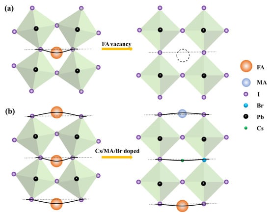
Figure 1.
Schematic diagram of lattice strain relief in CsMAFA perovskite: (a) formation of FA vacancy; (b) incorporation of multiple ions.
To further investigate the effect of Rb+ incorporation on the growth of CsMAFA perovskite films, X-ray diffraction measurements were taken. As shown in Figure 2, all components exhibited a typical perovskite peak near 14°. For the CsMAFA (component without Rb+) film, a typical characteristic peak appeared at 14.06°. The main reflection peak of α-FAPbI3 (14°) shifted to a higher angle, indicating that the doping of Cs+ caused the contraction of the MAFA-based perovskite lattice, which facilitated the release of lattice strain. Moreover, we noted small side peaks at 11.56° and 12.96°, corresponding to non-photoactive (δ-FAPbI3) and excess PbI2, respectively. This was a typical observation of the incomplete conversion of mixed-cation perovskites to the photoactive phase. Subsequently, when we introduced 5% of Rb+, the main reflection peak further shifted to 14.10° and the peak intensity increased, demonstrating that the introduction of Rb+ could further alleviate lattice distortion in the CsMAFA-based perovskite. In particular, the intensity of the δ-phase diminished when we introduced Rb+, and 5% of Rb+ suppressed the formation of the δ-phase most effectively, which indicated that a small amount of Rb+ was able to promote the CsMAFA-based perovskite crystallizing to the α-phase. Notably, the decrease in the small side peak at 12.96° may suggest that Rb+ consumed the residual PbI2 reaction to form the Rb-containing mixture [28]. Moreover, excessive Rb+ may compete with the incorporation of Cs+ into the perovskite lattice by forming a stable mixed Cs/Rb hexagonal phase.
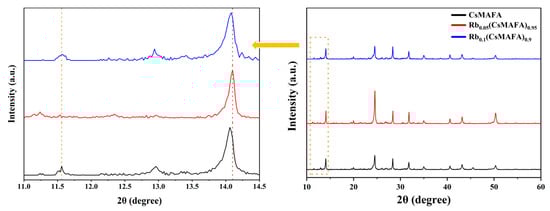
Figure 2.
XRD spectra of the Rbx(CsMAFA)1−x perovskite with different Rb ratios.
The main reflection peak shifted slightly to 14.08° and the diffraction peak’s intensity decreased when the Rb+ concentration was increased to 10%. Therefore, excessive Rb+ may be detrimental to the crystallization of CsMAFA-based perovskite. In terms of crystal quality, the optimal ration of Rb+ was 5%.
It is well known that films with a large grain size and fewer grain boundaries are essential for reducing carrier recombination and enhancing carrier mobility, as pinholes or cracks tend to form non-radiative recombination centers that adversely affect devices’ performance. The surface morphologies of CsMAFA and Rb0.05(CsMAFA)0.95 were investigated using scanning electron microscopy (SEM) (Figure 3a,b). As shown in Figure 3c,d, the average grain size of the Rb0.05(CsMAFA)0.95 film improved from 211 nm to 226 nm, which indicates that Rb+ promoted crystallization and matched the XRD result. Energy Dispersive Spectroscopy (EDS) on the surface of the Rb 0.05(CsMAFA)0.95 film also confirmed the presence of Rb+, as shown in Figure 3e. Hence, the addition of an optimal proportion of Rb+ to the perovskite precursor solution could effectively control the crystallization process of the film, which was beneficial for yielding highly crystalline and crack-free perovskite films to improve photodetectors’ performance.
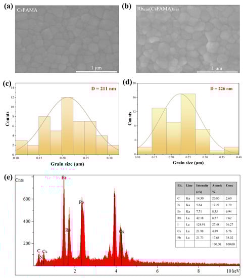
Figure 3.
Scanning electron microscope images of the mixed-cation Rbx(CsMAFA)(1−x) films incorporated with (a) 0% Rb+ and (b) 5% Rb+. Grain size statistics for Rbx(CsMAFA)(1−x) films incorporated with (c) 0% Rb+ and (d) 5% Rb+. (e) EDS on the surface of the Rb0.05(CsMAFA)0.95 thin film showing the elemental composition.
Figure 4b shows the UV–Vis absorption spectra of CsMAFA perovskite films with different Rb+ ratios. The CsMAFA film has a strong absorbance in the region of wavelengths less than 450 nm, and the absorption band could extend beyond 800 nm. The Rb0.05(CsMAFA)0.95 film’s absorbance significantly improved in the region of wavelengths less than 752 nm, with a band gap of 1.65 eV calculated using the Tauc formula (Figure 4c). The absorbance increase stemmed from the increase in grain size and the reduction in grain boundaries and cracks. It was shown that the optimal ratio of Rb+ helped induce crystallization of the photoactive phase and improve the film quality, which was beneficial for enhancing the device’s charge collection efficiency. Increasing charge collection efficiency enables detectors to output larger light-to-dark ratios.
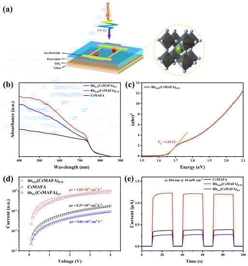
Figure 4.
(a) Schematic diagram of photodetector’s structure; (b) UV–vis absorption spectra of Rbx(CsMAFA)(1−x) perovskite thin films; (c) the calculated optical band gap based on the Tauc equation; (d) photoconductivity measurement of the devices based on Rbx(CsMAFA)(1−x) perovskite thin films; (e) the photodetectors’ switching properties under a 564 nm and 10 mW cm−2 light illumination.
Detectors’ charge collection efficiencies can be evaluated using the carrier mobility–lifetime (μτ) product. To quantitatively characterize the effect of different Rb+ ratios on the detector’s charge collection efficiency, we fabricated three devices separately and performed photoconductivity measurements. In this paper, we used a gold interdigitated electrode to collect carriers, as shown in Figure 4a. Alternating arc-shaped electric fields are formed between interdigitated electrodes at each end, and carriers are transported between interdigitated electrodes at the top of the perovskite layer. Electrons and holes may bounce between two electrodes repeatedly, resulting in recirculation and abnormally high photoconductive gain. As shown in Figure 4d, we used a modified Hecht equation to fit the photoconductivity curves and extract the µτ values. The Hecht equation is expressed as follows [37]:
where I0 is the saturated photocurrent and d is the distance between electrodes [38]. The calculated µτ values of CsMAFA, Rb0.05(CsMAFA)0.95, and Rb0.1(CsMAFA)0.9 were 8.37 × 10⁻⁶ cm2 V−1, 1.03 × 10⁻⁵ cm2 V−1, and 9.01 × 10⁻⁶ cm2 V−1, respectively. The Rb0.05(CsMAFA)0.95 device yielded the highest µτ value, further demonstrating the beneficial effect of small amounts of Rb+ on the crystallization of films. Figure 4e shows the photocurrent responses of three photodetectors under a light illumination of 10 mW cm−2 and a bias of 4 V. The calculated on–off values for CsMAFA, Rb0.05(CsMAFA)0.95, and Rb0.1(CsMAFA)0.9 were 64, 1519, and 37, respectively. Notably, the photocurrent of the Rb0.1(CsMAFA)0.9 device decreased instead, which could probably be attributed to cesium’s tendency to form a stable Cs0.5Rb0.5PbI3 phase in the presence of excess rubidium [28]. As a result, an optimal amount of Rb+ could yield the highest switching ratio. Based on the above analysis, we determined that the optimal Rb+ ratio was 5% and measured the current–voltage (I–V) characteristics (Figure 5a) of the prepared photodetector under different light irradiation wavelengths. The typical ohmic characteristics of the I–V curves indicated that a good ohmic contact was formed between the perovskite and the Au electrode. The increase in conductivity under light irradiation was attributed to an increase in the electron–hole pair concentration; the current signal generated by an external voltage was detectable. Responsivity (R) is an important parameter characterizing the ability of a photodetector to convert photons into a current signal, and it can be calculated using the following equation [39]:
where Ip is the photocurrent, Id is the dark current, P is the light intensity, and S is the effective area of the device. Figure 5b shows variations in R versus light intensity. The photocurrent increased linearly with increasing light intensity under 454 nm illumination, whereas the responsivity decreased with increasing light intensity due to the dominance of bimolecular recombination under strong light [40]. The maximum R was 11.8 mA W−1 at a light intensity of 0.5 mW cm−2. Linear dynamic range (LDR) is a figure-of-merit that represents the range of light intensity over which a detector can output photocurrent linearly. LDR can be calculated using the following formula [41]:
where Pmax is the saturation light intensity under which the photocurrent begins to deviate from linearity and Pmin is the initial light intensity. Figure 5b shows that the photocurrent increased linearly with increasing light intensity from approximately 0.5 mW cm−2 to above 20 mW cm−2, yielding an LDR of 32 dB. We further evaluated the specific detectivity, which is a parameter characterizing a detector’s ability to detect weak light and is calculated using the following expression:
where R is the responsivity, e is the unit charge, Id is the dark current, and S is the active area. Figure 5c shows the variation in D* with light intensity. The maximum value of D* was 5.33 × 10¹¹ Jones under light irradiation at 454 nm, 0.5 mW cm−2, which proves its potential application in weak near-ultraviolet light sensing and imaging. External quantum efficiency (EQE) is also a key photodetector parameter and is defined as the ratio of the number of electron–hole pairs collected by the external circuit to the number of incident photons. It is calculated as follows:
where R is the responsivity, h is Planck’s constant, c is the speed of light, e is the elementary charge, and λ is the wavelength of the incident light. The EQE versus wavelength is shown in Figure 5d. The EQE reached a peak of 1.5% at a wavelength of 454 nm, with a D* up to 2.49 × 10¹¹ Jones due to the high absorption coefficient in the near-UV band. The EQE gradually decreased in the region of wavelengths above 632 nm; the lowest D* was 9.38 × 10⁸ Jones at 868 nm.

Figure 5.
(a) I–V curves of the Rb0.05(CsMAFA)0.95 perovskite photodetector under 454 nm light illumination with different illumination intensities. (b) Photocurrent and responsivity versus light intensity at 454 nm light illumination under 4 V. (c) D* versus light intensity at 454 nm light illumination under 4 V. (d) EQE and D* versus wavelength at 10 mW cm−2 under 4 V.
Moreover, response time is a key parameter that represents the speed of detecting transient light signals. Rise time is the time duration from 10% to 90% of the saturation current. As shown in Figure 6a,b, we fitted the experimental curves of the rising and decay processes using a stretched exponential function [42]:
where I0 is the amplitude of the current and τ is the time constant. The calculated rise time (τr) and fall time (τf) were 208.3 μs and 288.4 μs, respectively, which demonstrated the effective extraction of carriers at the interface between the perovskite and Au electrodes and the perovskite thin film’s high charge mobility. The quadruple-cation perovskite films’ ultra-fast response time and broad absorption spectrum from the ultraviolet to the near-infrared demonstrated their promising application as broadband photodetectors. A summary of the state-of-the-art research regarding perovskite photodetectors’ performance is presented in Table 1.
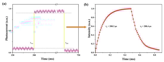
Figure 6.
(a) Photocurrent response of the photodetector with rising and decaying time. (b) The fitted curve of the rising and decay processes.

Table 1.
Summary of reported perovskite photodetectors.
The repeatability of photodetectors in detecting light is an important factor limiting their practical application. It is well known that detectors based on mixed-cation perovskite thin films suffer from severe baseline drift during continuous on–off due to ion migration and phase segregation. As shown in Figure 7, we measured the photodetector’s switching behavior under 564 nm light with a 4 V bias. The device showed no significant photocurrent decay during multiple on–off cycles with a maximum on–off ratio up to 7252 at 80 mW cm−2 light illumination; this demonstrated good photosensitive stability under ambient conditions.
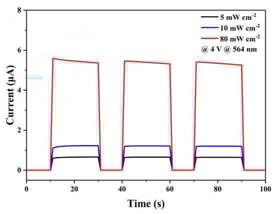
Figure 7.
Switching behavior of the photodetector based on Rb0.05(CsMAFA)0.95 quadruple-cation perovskite with different light intensities.
4. Conclusions
In conclusion, we developed a photodetector based on a mixed-cation perovskite thin film. The incorporation of an optimal Rb+ proportion into the precursor solution helped obtain highly crystalline perovskite films with large grain sizes and few grain boundaries. A reduction in nonradiative or undesired recombination improved the carrier mobility–lifetime product (μτ). Hence, the photodetector based on mixed-cation perovskite (Rb0.05(CsMAFA)0.95) thin film exhibited a good linear response over a light intensity range of 0.5 mW cm−2 to 20 mW cm−2 with a maximum responsivity of 11.8 mA W−1 and an excellent on–off ratio of up to 7252. Simultaneously, the photodetector showed a broad absorption spectrum between 400 and 765 nm, with a maximum D* of 5.33 × 10¹¹ Jones. The effective extraction of carriers at the interface between the perovskite and Au electrodes facilitated the device’s ultra-fast response time; the τr and the τf were 208.3 μs and 288.4 μs, respectively, with no significant decrease in photocurrent during multiple cycle measurements. These results verify perovskite’s potential as a next-generation high-performance photodetector.
Author Contributions
Conceptualization, Y.L.; methodology, Y.L.; software, W.W.; validation, Y.L.; formal analysis, Y.L. and J.Y.; investigation, W.W., Y.L. and J.Y.; resources, Y.L.; data curation, Y.L.; writing—original draft preparation, W.W.; writing—review and editing, Y.L.; visualization, W.W.; supervision, X.O.; project administration, Y.L.; funding acquisition, Y.L. All authors have read and agreed to the published version of the manuscript.
Funding
This research was funded by the National Key R&D Program of China (No. 2022YFB1902700); the National Natural Science Foundation of China (No. 11875129); the Fund of State Key Laboratory of Intense Pulsed Radiation Simulation and Effect (No. SKLIPR1810); the Fund of Innovation Center of Radiation Application (No. KFZC2020020402); the Fund of State Key Laboratory of Nuclear Physics and Technology, Peking University (No. NPT2020KFY08); and the Joint Innovation Fund of China National Uranium Co., Ltd.–State Key Laboratory of Nuclear Resources and Environment, East China University of Technology (No. 2022NRE-LH-02).
Institutional Review Board Statement
Not applicable.
Informed Consent Statement
Not applicable.
Data Availability Statement
Not applicable.
Conflicts of Interest
The authors declare no conflict of interest.
References
- Park, N.-G. Perovskite solar cells: An emerging photovoltaic technology. Mater. Today 2015, 18, 65–72. [Google Scholar] [CrossRef]
- Wang, F.; Zou, X.; Xu, M.; Wang, H.; Wang, H.; Guo, H.; Guo, J.; Wang, P.; Peng, M.; Wang, Z.; et al. Recent Progress on Electrical and Optical Manipulations of Perovskite Photodetectors. Adv. Sci. 2021, 8, 2100569. [Google Scholar] [CrossRef] [PubMed]
- Zhao, D.; Yu, Y.; Wang, C.; Liao, W.; Shrestha, N.; Grice, C.R.; Cimaroli, A.J.; Guan, L.; Ellingson, R.J.; Zhu, K.; et al. Low-bandgap mixed tin-lead iodide perovskite absorbers with long carrier lifetimes for all-perovskite tandem solar cells. Nat. Energy 2017, 2, 17018. [Google Scholar] [CrossRef]
- Chen, Q.; De Marco, N.; Yang, Y.; Song, T.B.; Chen, C.C.; Zhao, H.X.; Hong, Z.R.; Zhou, H.P.; Yang, Y. Under the spotlight: The organic-inorganic hybrid halide perovskite for optoelectronic applications. Nano Today 2015, 10, 355–396. [Google Scholar] [CrossRef]
- Lyu, M.; Yun, J.-H.; Cai, M.; Jiao, Y.; Bernhardt, P.V.; Zhang, M.; Wang, Q.; Du, A.; Wang, H.; Liu, G.; et al. Organic-inorganic bismuth (III)-based material: A lead-free, air-stable and solution-processable light-absorber beyond organolead perovskites. Nano Res. 2016, 9, 692–702. [Google Scholar] [CrossRef]
- Vijayakanth, T.; Liptrot, D.J.; Gazit, E.; Boomishankar, R.; Bowen, C.R. Recent Advances in Organic and Organic-Inorganic Hybrid Materials for Piezoelectric Mechanical Energy Harvesting. Adv. Funct. Mater. 2022, 32, 2109492. [Google Scholar] [CrossRef]
- Wang, Y.; He, J.; Chen, H.; Chen, J.; Zhu, R.; Ma, P.; Towers, A.; Lin, Y.; Gesquiere, A.J.; Wu, S.-T.; et al. Ultrastable, Highly Luminescent Organic-Inorganic Perovskite-Polymer Composite Films. Adv. Mater. 2016, 28, 10710–10717. [Google Scholar] [CrossRef]
- Kojima, A.; Teshima, K.; Shirai, Y.; Miyasaka, T. Organometal Halide Perovskites as Visible-Light Sensitizers for Photovoltaic Cells. J. Am. Chem. Soc. 2009, 131, 6050–6051. [Google Scholar] [CrossRef] [PubMed]
- Park, J.; Kim, J.; Yun, H.-S.; Paik, M.J.; Noh, E.; Mun, H.J.; Kim, M.G.; Shin, T.J.; Seok, S.I. Controlled growth of perovskite layers with volatile alkylammonium chlorides. Nature 2023, 616, 724–730. [Google Scholar] [CrossRef]
- Haruyama, J.; Sodeyama, K.; Han, L.; Tateyama, Y. Termination Dependence of Tetragonal CH3NH3PbI3 Surfaces for Perovskite Solar Cells. J. Phys. Chem. Lett. 2014, 5, 2903–2909. [Google Scholar] [CrossRef]
- Kubicki, D.J.; Prochowicz, D.; Hofstetter, A.; Saski, M.; Yadav, P.; Bi, D.; Pellet, N.; Lewinski, J.; Zakeeruddin, S.M.; Gratzel, M.; et al. Formation of Stable Mixed Guanidinium-Methylammonium Phases with Exceptionally Long Carrier Lifetimes for High-Efficiency Lead Iodide-Based Perovskite Photovoltaics. J. Am. Chem. Soc. 2018, 140, 3345–3351. [Google Scholar] [CrossRef] [PubMed]
- Long, R.; Liu, J.; Prezhdo, O.V. Unravelling the Effects of Grain Boundary and Chemical Doping on Electron-Hole Recombination in CH3NH3PbI3 Perovskite by Time-Domain Atomistic Simulation. J. Am. Chem. Soc. 2016, 138, 3884–3890. [Google Scholar] [CrossRef] [PubMed]
- Conings, B.; Drijkoningen, J.; Gauquelin, N.; Babayigit, A.; D’Haen, J.; D’Olieslaeger, L.; Ethirajan, A.; Verbeeck, J.; Manca, J.; Mosconi, E.; et al. Intrinsic Thermal Instability of Methylammonium Lead Trihalide Perovskite. Adv. Energy Mater. 2015, 5, 1500477. [Google Scholar] [CrossRef]
- Pang, S.; Hu, H.; Zhang, J.; Lv, S.; Yu, Y.; Wei, F.; Qin, T.; Xu, H.; Liu, Z.; Cui, G. NH2CH═NH2PbI3: An Alternative Organolead Iodide Perovskite Sensitizer for Mesoscopic Solar Cells. Chem. Mater. 2014, 26, 1485–1491. [Google Scholar] [CrossRef]
- Stoumpos, C.C.; Malliakas, C.D.; Kanatzidis, M.G. Semiconducting Tin and Lead Iodide Perovskites with Organic Cations: Phase Transitions, High Mobilities, and Near-Infrared Photoluminescent Properties. Inorg. Chem. 2013, 52, 9019–9038. [Google Scholar] [CrossRef]
- Borriello, I.; Cantele, G.; Ninno, D. Ab initio investigation of hybrid organic-inorganic perovskites based on tin halides. Phys. Rev. B 2008, 77, 235214. [Google Scholar] [CrossRef]
- Haeger, T.; Heiderhoff, R.; Riedl, T. Thermal properties of metal-halide perovskites. J. Mater. Chem. C 2020, 8, 14289–14311. [Google Scholar] [CrossRef]
- Cheng, W.J.; He, X.; Wang, J.G.; Tian, W.; Li, L. N-(2-aminoethyl) Acetamide Additive Enables Phase-Pure and Stable alpha-FAPbI(3) for Efficient Self-Powered Photodetectors. Adv. Mater. 2022, 34, 2208325. [Google Scholar] [CrossRef]
- Jeong, J.; Kim, M.; Seo, J.; Lu, H.; Ahlawat, P.; Mishra, A.; Yang, Y.; Hope, M.A.; Eickemeyer, F.T.; Kim, M.; et al. Pseudo-halide anion engineering for α-FAPbI3 perovskite solar cells. Nature 2021, 592, 381–385. [Google Scholar] [CrossRef]
- Chen, H.; Chen, Y.; Zhang, T.; Liu, X.; Wang, X.; Zhao, Y. Advances to High-Performance Black-Phase FAPbI(3) Perovskite for Efficient and Stable Photovoltaics. Small Struct. 2021, 2, 2000130. [Google Scholar] [CrossRef]
- Jeon, N.J.; Noh, J.H.; Yang, W.S.; Kim, Y.C.; Ryu, S.; Seo, J.; Seok, S.I. Compositional engineering of perovskite materials for high-performance solar cells. Nature 2015, 517, 476–480. [Google Scholar] [CrossRef] [PubMed]
- Saliba, M.; Matsui, T.; Seo, J.Y.; Domanski, K.; Correa-Baena, J.P.; Nazeeruddin, M.K.; Zakeeruddin, S.M.; Tress, W.; Abate, A.; Hagfeldt, A.; et al. Cesium-containing triple cation perovskite solar cells: Improved stability, reproducibility and high efficiency. Energy Environ. Sci. 2016, 9, 1989–1997. [Google Scholar] [CrossRef] [PubMed]
- Knight, A.J.; Borchert, J.; Oliver, R.D.J.; Patel, J.B.; Radaelli, P.G.; Snaith, H.J.; Johnston, M.B.; Herz, L.M. Halide Segregation in Mixed-Halide Perovskites: Influence of A-Site Cations. ACS Energy Lett. 2021, 6, 799–808. [Google Scholar] [CrossRef] [PubMed]
- Braly, I.L.; Stoddard, R.J.; Rajagopal, A.; Uhl, A.R.; Katahara, J.K.; Jen, A.K.Y.; Hillhouse, H.W. Current-Induced Phase Segregation in Mixed Halide Hybrid Perovskites and its Impact on Two-Terminal Tandem Solar Cell Design. ACS Energy Lett. 2017, 2, 1841–1847. [Google Scholar] [CrossRef]
- The, D.; Mulmudi, H.K.; Wu, Y.; Fu, X.; Shen, H.; Peng, J.; Wu, N.; Nguyen, H.T.; Macdonald, D.; Lockrey, M.; et al. Light and Electrically Induced Phase Segregation and Its Impact on the Stability of Quadruple Cation High Bandgap Perovskite Solar Cells. ACS Appl. Mater. Interfaces 2017, 9, 26859–26866. [Google Scholar] [CrossRef]
- Brennan, M.C.; Draguta, S.; Kamat, P.V.; Kuno, M. Light-Induced Anion Phase Segregation in Mixed Halide Perovskites. ACS Energy Lett. 2018, 3, 204–213. [Google Scholar] [CrossRef]
- Bi, D.; Yi, C.; Luo, J.; Decoppet, J.-D.; Zhang, F.; Zakeeruddin, S.M.; Li, X.; Hagfeldt, A.; Gratzel, M. Polymer-templated nucleation and crystal growth of perovskite films for solar cells with efficiency greater than 21%. Nat. Energy 2016, 1, 16142. [Google Scholar] [CrossRef]
- Kubicki, D.J.; Prochowicz, D.; Hofstetter, A.; Zakeeruddin, S.M.; Graetzel, M.; Emsley, L. Phase Segregation in Cs-, Rb- and K-Doped Mixed-Cation (MA)(x)(FA)(1−x)Pbl(3) Hybrid Perovskites from Solid-State NMR. J. Am. Chem. Soc. 2017, 139, 14173–14180. [Google Scholar] [CrossRef]
- Khan, A.A.; Azam, M.; Eric, D.; Liang, G.X.; Yu, Z.N. Triple cation perovskite doped with the small molecule F4TCNQ for highly efficient stable photodetectors. J. Mater. Chem. C 2020, 8, 2880–2887. [Google Scholar] [CrossRef]
- Li, Z.; Yang, M.; Park, J.-S.; Wei, S.-H.; Berry, J.J.; Zhu, K. Stabilizing Perovskite Structures by Tuning Tolerance Factor: Formation of Formamidinium and Cesium Lead Iodide Solid-State Alloys. Chem. Mater. 2016, 28, 284–292. [Google Scholar] [CrossRef]
- Bischak, C.G.; Wong, A.B.; Lin, E.; Limmer, D.T.; Yang, P.; Ginsberg, N.S. Tunable Polaron Distortions Control the Extent of Halide Demixing in Lead Halide Perovskites. J. Phys. Chem. Lett. 2018, 9, 3998–4005. [Google Scholar] [CrossRef] [PubMed]
- The, D.; Wu, Y.; Shen, H.; Peng, J.; Fu, X.; Jacobs, D.; Wang, E.-C.; Kho, T.C.; Fong, K.C.; Stocks, M.; et al. Rubidium Multication Perovskite with Optimized Bandgap for Perovskite-Silicon Tandem with over 26% Efficiency. Adv. Energy Mater. 2017, 7, 1700228. [Google Scholar] [CrossRef]
- Saidaminov, M.I.; Kim, J.; Jain, A.; Quintero-Bermudez, R.; Tan, H.; Long, G.; Tan, F.; Johnston, A.; Zhao, Y.; Voznyy, O.; et al. Suppression of atomic vacancies via incorporation of isovalent small ions to increase the stability of halide perovskite solar cells in ambient air. Nat. Energy 2018, 3, 648–654. [Google Scholar] [CrossRef]
- Gao, H.-L.; Zhu, Y.-B.; Mao, L.-B.; Wang, F.-C.; Luo, X.-S.; Liu, Y.-Y.; Lu, Y.; Pan, Z.; Ge, J.; Shen, W.; et al. Super-elastic and fatigue resistant carbon material with lamellar multi-arch microstructure. Nat. Commun. 2016, 7, 12920. [Google Scholar] [CrossRef]
- Kong, W.; Zhao, C.; Huang, T.; Li, X.; Xing, J.; Yu, Z.; Yang, P.; Li, W.; Yu, W. Accurate Adjusting the Lattice Strain of Triple-Cation and Mixed-Halide Perovskites for High-Performance Photodetector. ACS Appl. Mater. Interfaces 2022, 14, 28154–28162. [Google Scholar] [CrossRef]
- Liu, D.; Luo, D.; Iqbal, A.N.; Orr, K.W.P.; Doherty, T.A.S.; Lu, Z.-H.; Stranks, S.D.; Zhang, W. Strain analysis and engineering in halide perovskite photovoltaics. Nat. Mater. 2021, 20, 1337–1346. [Google Scholar] [CrossRef]
- Many, A. High-field effects in photoconducting cadmium sulphide. J. Phys. Chem. Solids 1965, 26, 575–578. [Google Scholar] [CrossRef]
- Basirico, L.; Senanayak, S.P.; Ciavatti, A.; Abdi-Jalebi, M.; Fraboni, B.; Sirringhaus, H. Detection of X-Rays by Solution-Processed Cesium-Containing Mixed Triple Cation Perovskite Thin Films. Adv. Funct. Mater. 2019, 29, 1902346. [Google Scholar] [CrossRef]
- Wang, Y.; Song, L.; Chen, Y.; Huang, W. Emerging New-Generation Photodetectors Based on Low-Dimensional Halide Perovskites. ACS Photonics 2020, 7, 10–28. [Google Scholar] [CrossRef]
- Binet, F.; Duboz, J.Y.; Rosencher, E.; Scholz, F.; Härle, V. Mechanisms of recombination in GaN photodetectors. Appl. Phys. Lett. 1996, 69, 1202–1204. [Google Scholar] [CrossRef]
- Fang, Y.; Huang, J. Resolving Weak Light of Sub-picowatt per Square Centimeter by Hybrid Perovskite Photodetectors Enabled by Noise Reduction. Adv. Mater. 2015, 27, 2804–2810. [Google Scholar] [CrossRef] [PubMed]
- Singh, S.C.; Peng, Y.; Rutledge, J.; Guo, C. Photothermal and Joule-Heating-Induced Negative-Photoconductivity-Based Ultraresponsive and Near-Zero-Biased Copper Selenide Photodetectors. ACS Appl. Electron. Mater. 2019, 1, 1169–1178. [Google Scholar] [CrossRef] [PubMed]
- Mueller, T.; Xia, F.; Avouris, P. Graphene photodetectors for high-speed optical communications. Nat. Photonics 2010, 4, 297–301. [Google Scholar] [CrossRef]
- Basyooni, M.A.; Zaki, S.E.; Shaban, M.; Eker, Y.R.; Yilmaz, M. Efficient MoWO3/VO2/MoS2/Si UV Schottky photodetectors; MoS2 optimization and monoclinic VO2 surface modifications. Sci. Rep. 2020, 10, 15926. [Google Scholar] [CrossRef] [PubMed]
- Waleed, A.; Tavakoli, M.M.; Gu, L.; Hussain, S.; Zhang, D.; Poddar, S.; Wang, Z.; Zhang, R.; Fan, Z. All Inorganic Cesium Lead Iodide Perovskite Nanowires with Stabilized Cubic Phase at Room Temperature and Nanowire Array-Based Photodetectors. Nano Lett. 2017, 17, 4951–4957. [Google Scholar] [CrossRef]
- Zhang, X.; Yang, S.; Zhou, H.; Liang, J.; Liu, H.; Xia, H.; Zhu, X.; Jiang, Y.; Zhang, Q.; Hu, W.; et al. Perovskite-Erbium Silicate Nanosheet Hybrid Waveguide Photodetectors at the Near-Infrared Telecommunication Band. Adv. Mater. 2017, 29, 1604431. [Google Scholar] [CrossRef]
- Dong, Y.; Gu, Y.; Zou, Y.; Song, J.; Xu, L.; Li, J.; Xue, J.; Li, X.; Zeng, H. Improving All-Inorganic Perovskite Photodetectors by Preferred Orientation and Plasmonic Effect. Small 2016, 12, 5622–5632. [Google Scholar] [CrossRef]
- Zeng, J.; Zhou, H.; Liu, R.; Wang, H. Combination of solution-phase process and halide exchange for all-inorganic, highly stable CsPbBr3 perovskite nanowire photodetector. Sci. China-Mater. 2019, 62, 65–73. [Google Scholar] [CrossRef]
- Tang, Y.Y.; Liang, M.L.; Chang, B.D.; Sun, H.Y.; Zheng, K.B.; Pullerits, T.; Chi, Q.J. Lead-free double halide perovskite Cs3BiBr6 with well-defined crystal structure and high thermal stability for optoelectronics. J. Mater. Chem. C 2019, 7, 3369–3374. [Google Scholar] [CrossRef]


Disclaimer/Publisher’s Note: The statements, opinions and data contained in all publications are solely those of the individual author(s) and contributor(s) and not of MDPI and/or the editor(s). MDPI and/or the editor(s) disclaim responsibility for any injury to people or property resulting from any ideas, methods, instructions or products referred to in the content. |
© 2023 by the authors. Licensee MDPI, Basel, Switzerland. This article is an open access article distributed under the terms and conditions of the Creative Commons Attribution (CC BY) license (https://creativecommons.org/licenses/by/4.0/).