Abstract
The synthesis of crystals with a high surface-to-volume ratio is essential for innovative, high-performance electronic devices and sensors. The easiest way to achieve this in integrated devices with electronic circuits is through the synthesis of high-aspect-ratio nanowires aligned vertically to the substrate surface. Such surface structuring is widely employed for the fabrication of photoanodes for solar cells, either combined with semiconducting quantum dots or metal halide perovskites. In this review, we focus on wet chemistry recipes for the growth of vertically aligned nanowires and technologies for their surface functionalization with quantum dots, highlighting the procedures that yield the best results in photoconversion efficiencies on rigid and flexible substrates. We also discuss the effectiveness of their implementation. Among the three main materials used for the fabrication of nanowire-quantum dot solar cells, ZnO is the most promising, particularly due to its piezo-phototronic effects. Techniques for functionalizing the surfaces of nanowires with quantum dots still need to be refined to be effective in covering the surface and practical to implement. The best results have been obtained from slow multi-step local drop casting. It is promising that good efficiencies have been achieved with both environmentally toxic lead-containing quantum dots and environmentally friendly zinc selenide.
1. Introduction
Quantum dots (QDs) are nanometer-sized particles with sizes that are small enough to be comparable to the Bohr radius of the atoms that comprise their bulk material; usually, this represents no more than two orders of magnitude difference from the Angstrom unit [1]. To be applied in optoelectronic devices, QDs must be composed of semiconductor materials that offer high emission stability, optical gain, and size-adjustable wavelength shifts [2]. For example, early experiments on AlGaAs QDs on GaAs and InGaAs QDs on InP in the 1980s [3] proved to increase the optical gain by more than an order of magnitude. Optoelectronic devices that can be improved through the use of QDs are numerous, and their uses extend to biology and medicine because organic dyes are limited in exhibiting these properties and, therefore, are not suitable for many imaging and biosensing applications, such as:
- Lasers.
- Semiconductor optical amplifiers.
- Modulators.
- Photodetectors.
- Quantum computing.
- Fluorescence spectroscopy.
- Biomedical imaging.
- Biosensors.
Nanowires (NWs) are widely used in innovative electronic devices, especially in the form of dense arrays of vertically aligned nanowires (VANWs) with a very high surface area to volume ratio, a feature that is essential for improving performance in optoelectronic [4] and photochemical devices [5]. The opportunity to combine quantum properties with nanoscale physics through the external functionalization of NWs with QDs may offer unprecedented photocurrent conversions in solid-state devices. For example, using the above combination, the responsivity of photodetectors has increased by more than a decade [6,7]. Furthermore, since Sandhu [8] published a short piece in Nature Nanotechnology about a three-fold increase in the power conversion efficiency (PCE) of solar cells made with ZnO VANWs functionalized with PbSe QDs [9], compared to a simple thin-film version of ZnO [10] (see Figure 1), significant efforts have been made in the fabrication of these types of nanowire–quantum dot hybrid solar cells (NWQDSCs). Still using ZnO-based VANWs coupled with PbS QDs, the PCE of the solar cells increased by 35% [11]. These dramatic improvements are the result of the combined effects of the aspect ratio of the ZnO NWs and the density of the QDs. In subsequent studies, even higher PCEs were obtained on devices based on the combination of ZnO NWs and PbS QDs, up to 6% and 8% under 1 sun illumination [12,13].
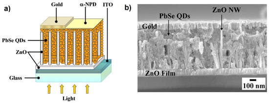
Figure 1.
(a) Typical device structure of a nanowire–quantum dot solar cell (NWQDSC) as proposed by Leschkies et al. (b) Cross-section SEM image of a NWQDSC based on ZnO NWs. Adapted with permission from Ref. [9]. Copyright 2009, American Institute of Physics.
Surface engineering does not always provide better results in light energy harvesting, as increasing the carrier path can increase the recombination of photogenerated charges. In [14], the nanostructured absorbent layer of SbS on the titania nanotubes conglomerates into medium-sized clusters when thermally annealed, increasing the carrier path; therefore, the efficiency of the nanostructured solar cell drops to 1.3% from the 2% value of the planar one. The complete functionalization of the NW surface with QDs is one of the main objectives that technology must pursue [15,16]. The use of QDs for the fabrication of flexible photovoltaic cells has already attracted a lot of attention due to the efficiency of QDs in collecting light; this was recently reviewed in 2019 and 2022, in terms of both efficiency and stability [17,18]. The use of NWs in solar cells has also recently been revised, mainly NWs of ZnO [19,20], due to the continuous progress in the wet chemistry of ZnO, which allows their easy fabrication on flexible and transparent substrates [21]. In this article, we will review the main optoelectronic materials, such as ZnO, TiO, SnO, used for surface engineering in photovoltaic cells functionalized with QDs and featuring improved PCEs. The goal is to provide the reader with a technical foundation to inspire the best strategies in terms of QD selection and nanowire functionalization techniques. This would enable NWQDSCs to match the performance of other types of solar cells, such as low-cost dye-sensitized solar cells, with PCE reported at around 12% under standard emulated sunlight [22], and recently pushed beyond the 15% threshold [23].
2. Quantum Dot Materials and Synthesis
QDs can be self-produced in the laboratory or purchased from chemical companies, such as Crystal Plex, Sony, Nagase, LG Display, Samsung Electronics, Thermo Fisher Scientific, DuPont, and many others. QD research is not limited to the academic environment, but the growing demand for better displays on smart TVs and mobile phones has prompted the industrial research system to invest a lot of resources in QDs. In fact, the global quantum dot market is expected to grow at a compound annual growth rate greater than 25% [24]. QDs are already available in many different semiconducting materials that are useful for optoelectronic devices, e.g., II–VI semiconductor compounds, such as cadmium selenide (CdSe), cadmium sulfide (CdS), cadmium telluride (CdTe), lead selenide (PbSe), zinc indium phosphide/zinc sulfide (ZnInP/ZnS), zinc cadmium selenide/zinc sulfide (ZnCdSe/ZnS); III–V compounds, such as indium arsenide (InAs); electronic materials, such as silicon or silicon dioxide; or bidimensional material, such as graphene, molybdenum disulfide (MoS) or very promising perovskite quantum dots (PQDs) still with some stability issues to be solved for large–scale use in commercial products. Among all of the used semiconducting materials, given the requirement of using environmentally friendly materials in large-scale industrial processes, there is a lot of interest in indium phosphide QDs [25]. Regarding innovatively advanced optoelectronic materials, it is worth mentioning biocompatible and highly stable diamond QDs. Their use in molecular bioimaging is already well proven [26]. Industrial research mainly focuses on light–emitting devices. For example, the Samsung Research Institute (SAIT) recently developed a blue–emitting ZnSe QLED with a 2–year lifespan at 100–nit luminance [27]. Some months ago, Zhijing Tech presented a prototype of a 75 inch television based on perovskite QD-colored pixels [28]. Thanks to these outstanding achievements, academic research has the opportunity to deploy low-cost industrial QDs for other important applications, such as photovoltaic energy. In the next two subsections, we will describe the two main techniques to synthesize QDs: the sol–gel route and organometallic deposition.
2.1. Sol–Gel Method
The cheapest and simplest method to synthesize QDs is based on sol–gel wet chemistry, where the chemical precursors react in a solution [29,30,31,32]. Colloidal solutions allow for multiple molecular reactions within the liquid volume and the kinetics can vary greatly. Given the size-dependent properties of QDs, it is necessary for the size distribution of the nanoparticles to be as narrow as possible (i.e., monodispersity). This requires the simultaneous inactivation of chemical reactions on the surface of the QDs within the solution. It is usually obtained by introducing capping molecules that, based on their physicochemical properties, confer the following attributes:
- Narrow size distribution.
- Solubility.
- Chemical inertness.
- Dielectric barrier.
- Surface trap filling.
The monodispersity requirement is especially true for light-emitting devices but is not as strictly necessary for light-harvesting applications, making the sol–gel method very suitable for fabricating QDs for NWQDSCs. In fact, in NWQDSCs, it is sufficient for the high energy level of the QD to be closer to the vacuum level than the conduction band of the electron transport layer (ETL), and that the reverse happens for the low energy level and the valence band of the hole transport layer (HTL). On the other hand, it is much more important to consider the effects of the capping molecule on the QD shell interface. The typical procedure involves dissolving a salt containing the desired elements that make up the QD, e.g., zinc acetate for ZnO QDs [33], and then slowly adding a basic solution (e.g., potassium hydroxide in ethanol) cooled to low temperatures (~5 C). Subsequent surface functionalization can be performed by mixing the sol–gel solution of QDs with DI water mixed with other molecules. QDs should be separated from unreacted precursors by centrifugation, ethanol washing, and drying.
2.2. Organometallic Synthesis
Organometallic compounds have been extensively employed in metal–organic chemical vapor deposition (MOCVD) for the growth of single crystalline films with thicknesses within the range of a QD diameter of 1–10 nm, regardless of their nature, i.e., insulators, semiconductors, or metals. This versatility originates from the large variety of organometallic compounds in nature. Organometallic synthesis is based on the hot-injection method, which involves the reaction between nutrient solvent solutions at high temperatures using non-polar solvents, mainly trioctylphosphine oxide (TOPO). This technique, even if it is more complex and costly, is able to produce higher quality QDs [34,35,36,37], with superior physicochemical properties, such as:
- Long-term stability.
- Monodispersity.
- High-quantum efficiency.
- Long luminescence lifetime.
- Electron paramagnetic resonance inactivity.
Organometallic techniques may also be used for the preparation of the capping layer of QDs. For example, using hydrophobic molecules, such as 2-(2-methoxyethoxy)acetate, may make ZnO QDs resistant to both chemical and biological environments [38].
2.3. Physical Deposition Systems
The initial research on devices based both on NWs and QDs assumed their integration during the NW growth. This technology has been well studied and documented [39] as it is essentially based on the synthesis of heterostructures through physical deposition techniques, such as molecular beam epitaxy [40], pulsed laser deposition [41], chemical vapor deposition [42], droplet epitaxy [43], and even multiple combinations of the aforementioned techniques [44]. In particular, physical epitaxial techniques allow for the strong control of material growth and, therefore, of QD lattice embedded into the nanowire body or grown onto its external facets with inherent mechanical strain, see Figure 2. As an example, InAs QDs grown on GaAs NW facets have demonstrated the availability of both single and double excitons in low-temperature photoluminescence spectroscopy [45,46]. This behavior is well modeled, considering the electromechanical field effects for tight-binding atomistic calculations [47]. On the other hand, such techniques usually require high temperatures and costly equipment and are more suitable for the production of highly performant photonic devices rather than cost-competitive solar cells [48].
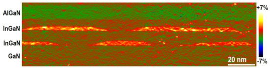
Figure 2.
HRTEM image of the out-of-plane strain by the geometric phase analysis of InGaN QDs embedded in the GaN lattice. Reprinted with permission from Ref. [49]. Copyright 2023, MDPI.
2.4. Quantum Dots Properties
QDs are very small nanoparticles with diameters of less than 20 nm; they may undergo electron quantum confinement, which leads to a change in the band gap energy of the bulk semiconductor material since the state distance in the k–space (Δk) proportional to the size of the QD (L):
where is the exciton effective mass:
For example, the widely studied silicon QDs are able to increase the energy level gap by 0.3 eV when halving their diameter from 8 to 4 nm [50]. A sketch of the gap change due to quantum confinement is reported in Figure 3.
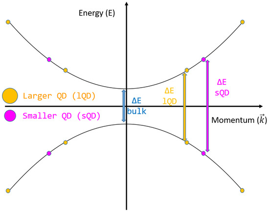
Figure 3.
Energy levels and quantum confinement in quantum dots.
In QDs, it is possible to observe multiple exciton generation when incoming photons are able to create more than a single electron–hole pair. QDs possess a built-in dipole due to the spatial separation of positive and negative charge carriers. Generally, the electrons concentrate in apex regions and the dipole points from the apex to the base. It is possible to prove it through mathematical modeling of the red shift of emitted photons under a dc bias or by measuring the dielectric dispersion, resulting in a dipole moment of about 10 eÅ for very small QDs (r < 2.5 nm) [51] or tens of eÅ for larger sizes [52].
3. Vertically Aligned Nanowire Synthesis
To produce a nanostructured layer as a 3D scaffold for absorbing light through sensitization with QDs, researchers mainly employ the following three semiconductor oxides:
- Titanium dioxide (TiO).
- Zinc oxide (ZnO).
- Tin oxide (SnO).
As can be seen from the physical properties summarized in Table 1, ZnO, which is the most used, as well as SnO, have a higher mobility than TiO; the latter is a low-cost and easy-to-process direct band gap semiconductor with a band structure and physical properties similar to ZnO. It is still receiving attention from solar cell researchers, as will be shown in the dedicated section; however, for the NWQDSC structures analyzed in this review, it is probably the least suitable material to choose.

Table 1.
Physical properties of nanostructured semiconducting oxides for solar cells.
In addition to mobility, the exciton lifetime is also important to consider in the nanostructured versions of these semiconductor materials. It is worth noting that in the literature, a decrease in the recombination lifetime has been reported for TiO nanotubes compared to TiO nanoparticles [57]; however, the inverse effect has been demonstrated for tin oxide nanowires [58], making them very strong competitors to ZnO, but with a more complex manufacturing process.
3.1. TiO
This material, especially in the form of nanotubes, is widely used as an electron transport layer in dye-QD-sensitized solar cells; however, the crucial problem of electron mobility, as reported in Table 1, is partially compensated for by the very long recombination lifetime, which guarantees a good charge extraction at the metallic contacts [59]. The low charge mobility in standard TiO-based dye-sensitized solar cells (DSSCs) is due to the charge transfer at grain interfaces [57], a problem that is avoided in vertically aligned nanowires or nanotubes. The latter form is preferred for nanostructured TiO electrodes, both due to the greater sensitizing surface available and the consolidated and simple electrochemical synthesis route [60,61].
The TiO nanotubes obtained through the anodization of titanium plates in electrolytes containing fluoride ions can be produced with precise control over their diameters (see Figure 4) and strong confinement between the different nanotubes, giving life to highly ordered arrays of vertically aligned nanostructures [62]. This procedure, in addition to being relatively simple, is a cheap and easily scalable method and it mainly requires:
- Application of a tunable DC bias voltage to the titanium sheet (i.e., 10–20 V).
- An electrolyte solution (i.e., 0.1–0.4 M HF).
- Equilibrium between surface oxidation and dissolution rates.
- Continuous growth into vertically aligned nanopores or nanotubes (rate 0.5 m/h).
- Annealing in the air with slow heating and cooling rates (1–5 C/min).

Figure 4.
Scanning Electron Microscope (SEM) images of TiO nanotubes developed for DSSCs; (a) cross-Section. (b) Top view. Reproduced with permission from Ref. [57]. Copyright 2015, ACS pubs.
Figure 4.
Scanning Electron Microscope (SEM) images of TiO nanotubes developed for DSSCs; (a) cross-Section. (b) Top view. Reproduced with permission from Ref. [57]. Copyright 2015, ACS pubs.

By changing the chemical bath from dilute hydrofluoric acid to aqueous solutions of buffered fluorine salts, and increasing the anodizing time and voltage, it is possible to obtain ordered nanotubes of TiO with aspect ratios up to 1000, traversing the entire thickness of the original titanium plate to achieve freestanding nanotube membranes. Subsequent treatment with titanium chloride may enable the complete formation of TiO nanorods, if desired [63]. TiO nanostructures can even be synthesized from other material templates, such as ZnO, whose growth will be introduced in the next subsection. The liquid-phase deposition involving ammonium hexafluorotitanate hydrolysis enables the fast deposition of TiO on the ZnO nanorod shell and slow etching of the ZnO nanorod core [64].
3.2. ZnO
ZnO is a wide band gap (3.37 eV) semiconductor and has outstanding potential for optoelectronics in the near ultraviolet (UVA) range. Furthermore, ZnO nanowires, which belong to the wurtzite crystal group and exhibit a large piezopotential when mechanically stressed due to the non-centrosymmetric lattice, have been shown to be effective at increasing the charge collection efficiency in flexible solar cells due to the induced strain [65,66]. The realization of vertically aligned ZnO nanowires on different conductive surfaces is extremely simple and efficient, thanks to the discovery of galvanically assisted nucleation [67,68] in a standard equimolar solution of zinc nitrate and triethylamine. This technique allows for a large-scale array of vertically aligned nanowires to be fabricated at a low cost, even if the overall length is limited to a few microns, well beyond the length used in solar cell applications, usually between 1 and 2 m. However, there are many techniques used to increase the length of the grown ZnO nanowires, such as the addition of polyethylenimine (PEI) [69], the dynamic optimization of the temperature [70], or the use of other more expensive strategies, such as engineered thermoconvective growth in a solution [71], in which the nutrient solution is thermally stimulated by a local heater whose surface temperature is monitored, thanks to a small Pt100 temperature sensor inserted into a small hole drilled in the heater, and the synthesis in high-temperature ovens [72]. As will be explained in the section on solar cell performances, an excessive NW length can be detrimental because the charge collection efficiency decreases beyond a certain length, but the scattering length of the electrons, estimated by intensity-modulated photovoltage spectroscopy or the rise/fall times of the photocurrents induced by laser pulses, can be equal to 40–70 m [59], indicating that the electron collection efficiency in NWQDSCs cells can be ensured with a thin film of long NWs (see Figure 5d). However, there is no research work in this direction and researchers have concentrated on the much more important problem of surface passivation [73].
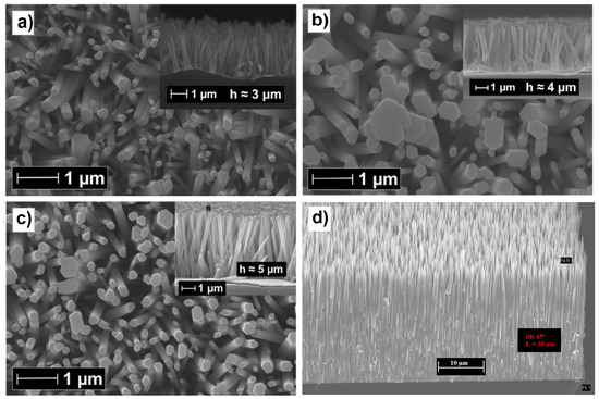
Figure 5.
(a) Top view SEM image of the ZnO nanorods grown at 90 C with a 2.5 mM equivalent solution of Zn(NO) and HMTA (cross-section in the top-right inset). (b) Top view SEM image of the ZnO nanorods grown at 70 C with a 2.5 mM equivalent solution of Zn(NO) and HMTA (cross-section in the top-right inset). (c) Top view SEM image of the ZnO nanorods grown by dynamic temperature with a 2.5 mM equivalent solution of Zn(NO) and HMTA (cross-section in the top-right inset). Adapted with permission from Ref. [70]. Copyright 2014, Nature Publishing Group. (d) Tilted view SEM image of long ZnO nanorods grown by thermoconvective heating at 90 C with a 30 mM equivalent solution of Zn(NO) and HMTA. Corresponding author, original research item.
3.3. SnO
SnO is a wide band gap material (E = 3.6 eV) with very high electron mobility and, therefore, it is suitable for the fabrication of nanostructured photoanodes in solar cells. The array of SnO nanorods for solar cells can be implemented with high-temperature physical deposition systems, such as pulsed laser deposition [74] and droplet epitaxy [75,76], or with low-temperature wet chemistry recipes [77,78,79]. It is also noteworthy that by employing chemical vapor synthesis at very high temperatures (>1000 C), it is possible to obtain well-aligned SnO nanotube arrays. In Figure 6, we reproduced SEM images of dye-sensitized solar cell photoanodes realized using this nanostructured material. These photoanodes exhibited a PCE of 2.53% [80].
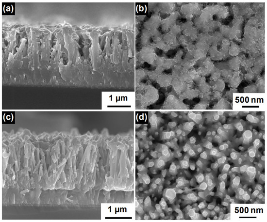
Figure 6.
(a) Cross-sectional and (b) top view images of SnO/BiVO core–shell NWs grown at 500 C, (c) cross-sectional and (d) top view images of SnO2/BiVO4 core–shell NWs grown at 600 C. Adapted with permission from Ref. [80]. Copyright 2018, American Chemical Society.
3.4. Quantum Dots Sensitizing Techniques
The main technique used for dispersing QDs on a surface consists of mechanically pressurizing a viscous solution of QDs through a sliding blade, and regulating the thickness of the applied layer by regulating the three main parameters: distance, speed, and temperature. On the other hand, it is evident that this method is not suitable for nanostructured surfaces with high aspect ratio nanowires, which are too brittle against the applied lateral forces. In fact, many other techniques exploit the unique and adjustable viscous liquid–solid interactions to produce, after the evaporation of the solvent, heterogeneous layers of different materials on a substrate with controlled thickness. In addition to blade casting, the main techniques for functionalizing surfaces with QDs are:
- Bar coating.
- Zone casting.
- Spin coating.
- Drop coating.
- Spray coating.
- Dip coating.
- Langmuir–Blodgett.
These methodologies depend on a unidirectional viscoelastic interaction between the substrate surface and the colloidal solution, which in our case should contain dispersed QDs. Bar coating is the main technique used in industrial production of large–area devices with organic molecules as active surface layer [81] and it schematically shown in Figure 7 regarding.
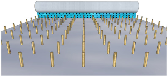
Figure 7.
Bar coating a colloidal solution with QDs over a sliding substrate with vertical nanowires.
Even if bar coating is suitable for controlling the molecular orientation, it is easy to implement and allows for multiple depositions, in the case of NWQDSCs, the solution’s shear forces must be adjusted so as not to damage the nanowire array; thus, the control of the meniscus of the solution adjacent to the substrate surface could be a very challenging step. Setting up a procedure for the QD sensitization of the VANW array by bar coating should be the final step for the production of low-cost NWQDSCs to commercialize. In the following subsections, we will focus on spray and dip coating techniques, mostly used in the academic research environment for the fabrication of solar cell prototypes.
3.4.1. Spray Coating
The process of spray coating the QDs to sensitize the nanostructured photoanodes is even more complex. Indeed, this technique, when used to fabricate organic solar cells, has often produced poor energy conversion efficiencies (<5%) attributable to the difficulty in creating a good interconnection between the nanoparticles and the solar cell surface [82,83]. Regarding this technique, in 2015, Prof. Kramer’s group published a fundamental work [84]. The study reported a room-temperature spray coating process of PbS QDs, demonstrating the control of nearly a single layer. The method yielded solar cells with an impressive performance of 8.1%. The overall manufacturing process, however, is very slow, and requires between 65 and 85 spray sequences (see Figure 8), where each sequence consists of the following procedures (just under one minute) for a total spray time of over an hour:
- 0.4 s QD monolayer spraying.
- 3 s pause.
- 1 s mercaptopropionic acid-spraying.
- 4 s methanol spraying.
- 40 s air blade drying.

Figure 8.
(a) Spray coating setup with three different nozzles for the three different spraying solutions: (1) fine mist spraying of colloidal QDs; (2) standard MPA–spraying; (3) standard methanol–spraying and (4) air drying. (b) Image of the QD sprayed coating according to the different number of sprayed layers. (c) Final device, ensemble of sixteen different sampling electrodes over its surface. A one-cent coin is shown for dimension reference. Copyright 2015, [84] Wiley.

3.4.2. Dip Coating/Langmuir–Blodgett Deposition
Dip coating is one of the most effective thin film deposition processes. As the name suggests, it is based on the controlled immersion of the substrate in a tank containing the desired coating materials dispersed in a colloidal solution. As can be seen in Figure 9a, the substrate is immersed in the solution at a certain speed (usually rather slowly), then a rest time must be implemented, which allows the formation of a capillarity bond at the substrate/solution interface (meniscus). The substrate is withdrawn from the vessel at a specific speed, which must prevent evaporation at the upper edge from changing the profile of the meniscus. Dip coating is a very effective process for fabricating NWQDSCs, as the substrate is vertically immersed in the solution and there is no risk of compromising the brittle array of vertically aligned nanowires. It is also low-cost and industrially scalable (see Figure 9). The main parameters to control the deposition are viscosity and surface tension. Dip coating was the technology used for the fabrication of the first NWQDSC [9], which involved the integration of 2 nm PbSe QDs on ZnO VANWs.
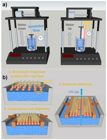
Figure 9.
(a) Dip coating technique with motorized substrate motions and set-up times for immersion and drying. (b) Langmuir–Blodgett deposition steps.
With the appropriate hydrophobic ligands, it is possible to locate QDs at the water/air interface with a single monolayer thickness. In this way, dip coating evolves into the Langmuir–Blodgett deposition, which allows transferring very dense monolayers of molecules to the desired target thanks to the control of the lateral and surface pressures on the Langmuir monolayer during the emergence of the substrate. The Langmuir–Blodgett technique is particularly suited for precisely coating nanometric rough surfaces with monolayers of QDs, as demonstrated in several papers [85,86]. On the other hand, it requires the functionalization of QDs with complex ligands, which can influence their optoelectronic properties due to potential vibroelectronic energy exchanges [87], which influence exciton dynamics and charge transport [88]. Moreover, to prevent compromising charge tunneling, it is usually preferable to use ligands with the shortest possible atomic chains [86].
3.5. Electronic Transport Properties of Surface-Functionalized Nanowires
Particular attention must be paid to the electron transport properties at the interface between the array nanowire and adjacent working QDs. If we consider a generic nanowire at the interface with a dielectric medium, there is a space charge region (shell in Figure 10a), due to the electric field created by the bending of the conduction band away from the Fermi level. In the case of semiconductor oxides (for example, ZnO nanowires), this phenomenon is enhanced by the high rate of reaction of the defective surface with the oxygen molecules present in the atmosphere, which, once absorbed on the surface of the nanowire, tend to accept the free electrons to form anions and, therefore, increase the depletion region (shell in Figure 10b). The influence of the partial pressure of oxygen on the depletion regions of ZnO nanowires and nanobelts has been confirmed by several studies [89,90,91], which certify the increase of the conductivity under vacuum conditions due to the desorption of oxygen, leading to increased mobility by avoiding surface traps [92]. Chemical adsorption on ZnO nanowires does not always have the same effect as oxygen molecules, i.e., as acceptors that capture electrons. For instance, a strong interaction between ZnO nanostructures and ambient humidity has been reported due to the chemisorption of hydroxyl groups on their external surfaces, which behave as donor molecules and increase the availability of electrons in the conductivity band [90].
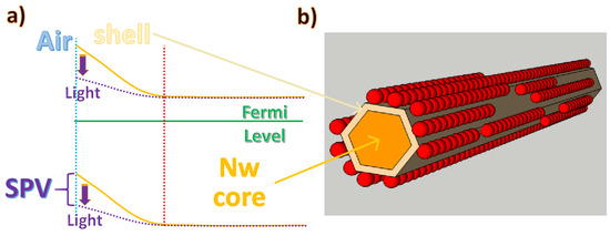
Figure 10.
(a) The effect of adsorbed acceptor molecules on nanowire electron energy levels. (b) Single nanowire superficially functionalized with quantum dots.
At standard atmospheric pressure, oxygen chemisorption at the rod surfaces captures free electrons (Figure 10b), increasing the space charge region and enhancing the distance between the Fermi level and the conduction band. This effect is detrimental to the efficiency of NWQDSCs efficiency since the nanowire layer usually acts as a photoanode and it needs to collect generated electrons. This is due to the work functions values of the used semiconductor materials. Indeed, as illustrated in the results reported in the next section of the review, the highest light harvesting efficiencies in NWQDSCs were obtained by creating a thin insulating layer on the nanowire surface prior to quantum dot functionalization and employing charge tunneling transport between the QDs and the NW body. Furthermore, it is worth noting that the promotion of electrons from the valence band to the conduction band directly within the bulk of the nanowire enables the tuning of the energy gap between the electron bands of QDs and NWs. In fact, when a light source creates electron–hole pairs, they can move by drift due to built-in fields or by diffusion. In a semiconductor, the majority carriers can drift at a greater length compared to minority carriers, but, in a thin nanowire body, they can reach the depleted shell in large numbers. As illustrated in Figure 10a, ZnO grown using standard wet chemistry recipes is an n-type semiconductor [93,94]. The photogenerated holes will then recombine with the adsorbed negative oxygen ions, which will be desorbed from the rod surface. This process reduces the energy barrier of a voltage, known as surface photovoltage (SPV), as depicted by the curly braces in Figure 10a; it also reduces the depletion volume and counteracts the drift of electrons caused by the built-in field. This behavior has been confirmed by photochemical studies on ZnO nanorods with functionalized surfaces [95], generating a lower SPV signal under the influence of UV illumination. Thus, after wet functionalization with QDs, as illustrated in previous subsections, by intense illumination at the appropriate wavelength, it would, in principle, be possible to change the surface potential by a desired amount.
4. Nanowires–Quantum Dot Solar Cells
To compare the performance of NWQDSCs in the literature, it is appropriate to consider the previous reviews that focused on similar nanostructured photoanodes [20,96] and quantum dot-sensitized solar cells (QDSSCs) [17,18], which, similar to dye-sensitized organic solar cells (DSSC), have a light-absorbing medium (dye or QD) embedded by two different materials, i.e., electron/hole transport materials or layers (ETM/HTM or ETL/HTL, respectively), dedicated to the transport of each excited charge (electron or hole). Such a device configuration would enable overcoming the transport limitations observed in QD thin films [97] assembled in standard quantum dot solar cells (QDSCs), where, to reach the metal contacts, both carriers drift along a thick layer of heterogeneous QDs, becoming trapped in the larger ones (lower band gap), resulting in a higher recombination rate. In the following Table 2, as a starting point for the analysis proposed in this work, we present a selection of the best articles mentioned in previous reviews.
Table 2.
The best solar cells from comprehensive reviews on QDs [17,18] and ZnO NW solar cells [20,96].
It is worth noting that interpenetrating NWQDSCs showed the best performance when fabricated using ZnO NWs and PbS QDs (PCE = 9.6% @ row 3 of Table 2). Moreover, in [104], the performance further improved to 10.8% by utilizing ZnO NWs with optimized areal density and surface treatment. This result is not surprising considering that in this type of solar cell the light harvesting involves the QDs ensemble and the light collection increases with the volume it occupies. It is important to note that in standard QDSCs (without interpenetrating NWs) the performances are much better (PCE = 15.3% [108], see the last row of Table 2). In this work, Song et al. focused on optimizing heterojunction bindings with a double QD deposition approach on TiO nanoparticles, using capping ligand-assisted self-assembly and on-purpose metal oxyhydroxide adsorption sites. In this way, they were able to form a light-absorbing mesoporous structure (see Figure 11) that was capable of exceeding the 15% PCE threshold, which is the same record mentioned in the introduction achieved by standard DSSCs without QDs utilization. It is also important to note that the researchers employed Pb- and Cd-free “green” QDs: MgCl capped Zn–Cu–In–S–Se (ZCISSe) QDs.
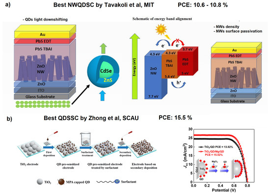
Figure 11.
(a) Optimized ZnO-based NWQDSCs with frequency down-shifting or density optimization. Reproduced with permission. Copyright 2019, [105] Royal Society of Chemistry. Copyright 2020, [106] Wiley. (b) Double ligand-assisted self-assembly approach on TiO NPs (drop-casting deposition), allowing increased surface coverage (almost 40% more) and relative solar cell performances. Adapted with permission from Refs. [108,109]. Copyright 2019/2021, American Chemical Society.
To understand the development possibilities of NWQDSCs, it is enough to mention that the best improvements to NWQDSCs have been made by Dr. Tavakoli’s group at the Massachusetts Institute of Technology, using the combination of ZnO NWs–PbS QDs [105,106] (see Figure 11a). In 2019, they implemented a UV light down-shifting layer (CdSe/ZnS QDs) [105], and in 2020, they optimized the surface area and areal density of NWs [106]. However, these very brilliant techniques have never been combined together in a new solar cell. Other recent studies report the use of different types of nanowires [110] or quantum dots on NWs of ZnO [111], but with poor results (PCE < 1%); therefore, we concentrate our further comparative analysis on solar cells with nanowires embedded in perovskite layers or functionalized with perovskite QDs (PQDs) (see Table 3 and Table 4).
Table 3.
Recent papers on perovskite solar cells based on semiconducting VANWs as ETL.
Moreover, when considering solar cells based on single-junction synthetic halide perovskites that utilize planar defect-engineered semiconducting charge transport layers, the overall PCE increased from 3.8% to 25.5% between 2009 and today [116]. In this context, the effect of interpenetrating ZnO NWs does not seem to be so positive if only the best overall efficiency results are sought. For example, in [117,118], using as ETL, respectively, a CuCl/MDACl superficially modified tin oxide planar film, PCEs of 20.3% and 22.3% were obtained as the best efficiency values, even with excellent temporal stability and reversible behavior. Moreover, as can be seen in Table 3, the efficiency of perovskite solar cells using NWs (all ZnO–based) does not exceed the threshold of 20%. On the other hand, in all of the cited works, the positive effect of the nanostructured electrode compared to the planar one is well understood. For example, in [104], the planar version has a 25% lower short-circuit current than the nanostructured version. Indeed, wide bandgap nanowires with high electron and hole mobility, when used as photoanodes/cathodes, are expected to strongly favor the collection of charges excited by the photon-absorbing layer. Thus, we attribute the fact that the efficiency of NWQDSCs is not yet superior to that of solar cells with other architectures to the complexity of combining accurate models of the embedded QDs carrier transport mechanisms [119] with the complex light-trapping effects of the three-dimensional structure [120]. Even the ability to control the non-perfect uniformity of samples obtained through low-cost nanofabrication processes with wet–chemistry recipes can play a fundamental role [121].
Table 4.
Best papers on solar cells with the addition of perovskite quantum dots improving PCE and stability extrapolated from the review [122].
Table 4.
Best papers on solar cells with the addition of perovskite quantum dots improving PCE and stability extrapolated from the review [122].
| Fabrication Technique | Reference | J | V | PCE |
|---|---|---|---|---|
| Type of PQDs | Year | [mA/cm] | [V] | [%] |
| Spin coating | [123] | 23.4 | 1.15 | 18.3/21.5 * |
| [2019] | ||||
| Spin coating | [124] | 23.86 | 1.11 | 18.4/19.5 * |
| [2019] | ||||
| Spin coating | [125] | 23.4 | 1.14 | 19.5/21.1 * |
| [2019] | ||||
| Spin coating | [126] | 23.8 | 1.07 | 18.2/20.06 * |
| [2020] |
* Increased Time-Stability to Humidity.
In Table 4, extrapolated from the review [122], we present the results obtained from the application of PQDs in solar cells. Again, the overall efficiency is not at the level of bulk perovskite-based solar cells [127]; however, this type of QD is able to increase the light-harvesting efficiency as a frequency down-shifting layer for c-Si solar cells [128], and above all, act as a stabilizing interlayer between the perovskite and the HTL material. Thus, it holds great promise as a powerful tool for the advancement of new generations of NWQDSCs. As the last point to underline, we highlight the potential of fabricating piezoelectric VANWs as photoanodes of flexible solar cells, as the role of the piezopotential at the ETL interface has been shown to effectively increase the PCE by more than 13% (see Figure 12). This result is higher than predictions of complex nanofabrication techniques for light trapping, which, at best, promise an increase in efficiency of no more than 11% [129].
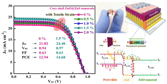
Figure 12.
ZnO@ZnS core–shell vertically aligned nanorods on a flexible substrate, allowing PCE improvement from 12.94% to 14.68%, utilizing the piezopotential induced by simple substrate bending. Copyright 2021, [114] Elsevier.
5. Conclusions and Outlook
Solar cells based on the combination of semiconducting NWs and QDs have not yet received a dedicated review; they have only been mentioned in subsections of more general reviews on QDSCs, QDSSCs, or single-material ones (e.g., ZnO). Thus far, the best results have been obtained through the implementation of ZnO NWs, whose geometric characteristics (density, length, morphology, etc.) play important roles in the overall efficiency. Lead sulfide QDs have been shown to be the most effective light harvesters, with nanowire surface passivation as an essential manufacturing step to prevent current leakage at the interface between ZnO nanowires and PbS QDs. There are other promising but complex approaches to harvesting light energy, which are theoretically capable of exceeding the Shockley–Queisser limit, such as thermionic emitters with solar concentrating systems, but they are still at an embryonic level (PCE < 10% [130]). Research on NWQDSCs, which began 14 years ago with a PCE of 2%, has rapidly progressed to achieve a 5-fold increase, surpassing efficiencies greater than 10%, presenting the opportunity for NWQDSCs to be a part of multi-junction solar cells [131] as an additional design approach to surpass the Shockley–Queisser limit. The 10% goal, even if is not in line with the best results obtained on solution-processed planar solar cells, confirms NWQDSC as an excellent research field, which can lead to much more important results. Even considering the use of halide perovskites in the device structure, solar cells with vertically aligned nanostructured photoanodes do not compare to the best results of planar versions. On the other hand, in the great majority of the analyzed works, the use of vertically aligned nanostructured electrodes or the use of QDs as an absorbing element have proved successful. This suggests that the complexity of the overall system, which is challenging to accurately model, is preventing the performance of NWQDSCs from reaching not only a very good level but an excellent one. Furthermore, the latest results on solar cells employing cadmium- and lead-free QDs promise a good performance combined with low environmental toxicity; moreover, there is room for further development in more effective NWs-QDs interfaces, with improved surface coverage, charge collection efficiency, and unexplored coupling with perovskite QDs. From the authors’ perspective, future research in the field of NWQDSCs should be based on studying the following factors that influence their light-harvesting efficiency:
- A detailed analysis of charge mobility in nanowire bodies after surface functionalization with QDs. In the literature, very short nanowire lengths had a negative impact on the overall performance of NWQDSCs, contrary to what was theoretically expected.
- In-depth research on band gap engineering due to piezo-phototronic effects at the interface between NWs and QDs, with positive effects on solar cell efficiency.
- The use of photoanodes with embedded quantum dots, as discussed in Section 2.3, has never been attempted because of the expensive physical deposition techniques needed to realize them, but scientific interest remains open.
- Finally, one overlooked aspect is the combination of nanowires with PQDs, which has proven to be much more stable than the highly performing layered versions.
Author Contributions
Conceptualization, All authors; methodology, A.O.; resources, D.B.; writing—original draft preparation, A.O.; writing—review and editing, All authors; visualization, All authors. All authors have read and agreed to the published version of the manuscript.
Funding
A.O. acknowledges financial support from ATHENA European University (EPLUS2020–AG, Project 101004096). https://eu-athena.eu (accessed on 18 May 2023).
Acknowledgments
Authors acknowledge Falconi of the University of Rome “Tor Vergata” for granting permission to share common research findings in this review.
Conflicts of Interest
The authors declare no conflict of interest. The funders had no role in the design of the study; in the collection, analyses, or interpretation of data; in the writing of the manuscript, or in the decision to publish the results.
Abbreviations
The following abbreviations are used in this manuscript:
| QDs | quantum dots |
| NWs | nanowires |
| VANWs | vertically aligned nanowires |
| PCE | power conversion efficiency |
| NWQDSCs | nanowires–quantum dot solar cells |
References
- Bawendi, M.G.; Steigerwald, M.L.; Brus, L.E. The Quantum Mechanics of Larger Semiconductor Clusters (“Quantum Dots”). Annu. Rev. Phys. Chem. 1990, 41, 477–496. [Google Scholar] [CrossRef]
- Farzin, M.A.; Abdoos, H. A critical review on quantum dots: From synthesis toward applications in electrochemical biosensors for determination of disease-related biomolecules. Talanta 2021, 224, 121828. [Google Scholar] [CrossRef]
- Asada, M.; Miyamoto, Y.; Suematsu, Y. Gain and the threshold of three-dimensional quantum-box lasers. IEEE J. Quantum Electron. 1986, 22, 1915–1921. [Google Scholar] [CrossRef]
- Barettin, D.; Shtrom, I.V.; Reznik, R.R.; Mikushev, S.V.; Cirlin, G.E.; Auf der Maur, M.; Akopian, N. Direct Band Gap AlGaAs Wurtzite Nanowires. Nano Lett. 2023, 23, 895–901. [Google Scholar] [CrossRef] [PubMed]
- Magna, G.; Catini, A.; Kumar, R.; Palmacci, M.; Martinelli, E.; Paolesse, R.; di Natale, C. Conductive Photo-Activated Porphyrin-ZnO Nanostructured Gas Sensor Array. Sensors 2017, 17, 747. [Google Scholar] [CrossRef] [PubMed]
- Li, L.; Gu, L.; Lou, Z.; Fan, Z.; Shen, G. ZnO Quantum Dot Decorated Zn2SnO4 Nanowire Heterojunction Photodetectors with Drastic Performance Enhancement and Flexible Ultraviolet Image Sensors. ACS Nano 2017, 11, 4067–4076. [Google Scholar] [CrossRef]
- Li, H.; Xu, P.; Liu, D.; He, J.; Zu, H.; Song, J.; Zhang, J.; Tian, F.; Yun, M.; Wang, F. Low-voltage and fast-response SnO2 nanotubes/perovskite heterostructure photodetector. Nanotechnology 2021, 32, 375202. [Google Scholar] [CrossRef]
- Sandhu, A. Wired for efficiency. Nat. Nanotechnol. 2009. [Google Scholar] [CrossRef]
- Leschkies, K.S.; Jacobs, A.G.; Norris, D.J.; Aydil, E.S. Nanowire-quantum-dot solar cells and the influence of nanowire length on the charge collection efficiency. Appl. Phys. Lett. 2009, 95, 193103. [Google Scholar] [CrossRef]
- Leschkies, K.S.; Beatty, T.J.; Kang, M.S.; Norris, D.J.; Aydil, E.S. Solar Cells Based on Junctions between Colloidal PbSe Nanocrystals and Thin ZnO Films. ACS Nano 2009, 3, 3638–3648. [Google Scholar] [CrossRef]
- Jean, J.; Chang, S.; Brown, P.R.; Cheng, J.J.; Rekemeyer, P.H.; Bawendi, M.G.; Gradečak, S.; Bulović, V. ZnO Nanowire Arrays for Enhanced Photocurrent in PbS Quantum Dot Solar Cells. Adv. Mater. 2013, 25, 2790–2796. [Google Scholar] [CrossRef] [PubMed]
- Wang, H.; Desbordes, M.; Xiao, Y.; Kubo, T.; Tada, K.; Bessho, T.; Nakazaki, J.; Segawa, H. Highly Stable Interdigitated PbS Quantum Dot and ZnO Nanowire Solar Cells with an Automatically Embedded Electron-Blocking Layer. ACS Appl. Energy Mater. 2021, 4, 5918–5926. [Google Scholar] [CrossRef]
- Wang, H.; Kubo, T.; Nakazaki, J.; Kinoshita, T.; Segawa, H. PbS-Quantum-Dot-Based Heterojunction Solar Cells Utilizing ZnO Nanowires for High External Quantum Efficiency in the Near-Infrared Region. J. Phys. Chem. Lett. 2013, 4, 2455–2460. [Google Scholar] [CrossRef]
- Büttner, P.; Döhler, D.; Korenko, S.; Möhrlein, S.; Bochmann, S.; Vogel, N.; Mínguez-Bacho, I.; Bachmann, J. Solid state interdigitated Sb2S3 based TiO2 nanotube solar cells. RSC Adv. 2020, 10, 28225–28231. [Google Scholar] [CrossRef] [PubMed]
- Kuo, K.T.; Liu, D.M.; Chen, S.Y.; Lin, C.C. Core-shell CuInS2/ZnS quantum dots assembled on short ZnO nanowires with enhanced photo-conversion efficiency. J. Mater. Chem. 2009, 19, 6780–6788. [Google Scholar] [CrossRef]
- Cao, X.; Chen, P.; Guo, Y. Decoration of Textured ZnO Nanowires Array with CdTe Quantum Dots: Enhanced Light-Trapping Effect and Photogenerated Charge Separation. J. Phys. Chem. C 2008, 112, 20560–20566. [Google Scholar] [CrossRef]
- Du, Z.; Artemyev, M.; Wang, J.; Tang, J. Performance improvement strategies for quantum dot-sensitized solar cells: A review. J. Mater. Chem. A 2019, 7, 2464–2489. [Google Scholar] [CrossRef]
- Rasal, A.S.; Yadav, S.; Kashale, A.A.; Altaee, A.; Chang, J.Y. Stability of quantum dot-sensitized solar cells: A review and prospects. Nano Energy 2022, 94, 106854. [Google Scholar] [CrossRef]
- Xu, J.; Chen, Z.; Zapien, J.A.; Lee, C.S.; Zhang, W. Surface Engineering of ZnO Nanostructures for Semiconductor-Sensitized Solar Cells. Adv. Mater. 2014, 26, 5337–5367. [Google Scholar] [CrossRef]
- Consonni, V.; Briscoe, J.; Kärber, E.; Li, X.; Cossuet, T. ZnO nanowires for solar cells: A comprehensive review. Nanotechnology 2019, 30, 362001. [Google Scholar] [CrossRef]
- Skompska, M.; Zarȩbska, K. Electrodeposition of ZnO Nanorod Arrays on Transparent Conducting Substrates—A Review. Electrochim. Acta 2014, 127, 467–488. [Google Scholar] [CrossRef]
- Sharma, K.; Sharma, V.; Sharma, S.S. Dye-Sensitized Solar Cells: Fundamentals and Current Status. Nanoscale Res. Lett. 2018, 13, 381. [Google Scholar] [CrossRef] [PubMed]
- Ren, Y.; Zhang, D.; Suo, J.; Cao, Y.; Eickemeyer, F.T.; Vlachopoulos, N.; Zakeeruddin, S.M.; Hagfeldt, A.; Grätzel, M. Hydroxamic acid pre-adsorption raises the efficiency of cosensitized solar cells. Nature 2023, 613, 60–65. [Google Scholar] [CrossRef]
- The Business Research Company. Quantum Dot Global Market Report 2023; Technical Report; The Business Research Company: London, UK, 2023. [Google Scholar]
- Jo, J.H.; Jo, D.Y.; Lee, S.H.; Yoon, S.Y.; Lim, H.B.; Lee, B.J.; Do, Y.R.; Yang, H. InP-Based Quantum Dots Having an InP Core, Composition-Gradient ZnSeS Inner Shell, and ZnS Outer Shell with Sharp, Bright Emissivity, and Blue Absorptivity for Display Devices. ACS Appl. Nano Mater. 2020, 3, 1972–1980. [Google Scholar] [CrossRef]
- Montalti, M.; Cantelli, A.; Battistelli, G. Nanodiamonds and silicon quantum dots: Ultrastable and biocompatible luminescent nanoprobes for long-term bioimaging. Chem. Soc. Rev. 2015, 44, 4853–4921. [Google Scholar] [CrossRef] [PubMed]
- Kim, T.; Kim, K.H.; Kim, S.; Choi, S.M.; Jang, H.; Seo, H.K.; Lee, H.; Chung, D.Y.; Jang, E. Efficient and stable blue quantum dot light-emitting diode. Nature 2020, 586, 385–389. [Google Scholar] [CrossRef]
- Wu, X.G.; Ji, H.; Yan, X.; Zhong, H. Industry outlook of perovskite quantum dots for display applications. Nat. Nanotechnol. 2022, 17, 813–816. [Google Scholar] [CrossRef]
- Arachchige, I.U.; Brock, S.L. Sol–Gel Methods for the Assembly of Metal Chalcogenide Quantum Dots. Acc. Chem. Res. 2007, 40, 801–809. [Google Scholar] [CrossRef]
- Bera, D.; Qian, L.; Sabui, S.; Santra, S.; Holloway, P.H. Photoluminescence of ZnO quantum dots produced by a sol–gel process. Opt. Mater. 2008, 30, 1233–1239. [Google Scholar] [CrossRef]
- Jiang, H.; Yao, X.; Che, J.; Wang, M.; Kong, F. Preparation of ZnSe quantum dots embedded in SiO2 thin films by sol–gel process. Ceram. Int. 2004, 30, 1685–1689. [Google Scholar] [CrossRef]
- Lin, K.F.; Cheng, H.M.; Hsu, H.C.; Lin, L.J.; Hsieh, W.F. Band gap variation of size-controlled ZnO quantum dots synthesized by sol–gel method. Chem. Phys. Lett. 2005, 409, 208–211. [Google Scholar] [CrossRef]
- Chen, X.; Wang, Q.; Wang, X.J.; Li, J.; Xu, G.B. Synthesis and performance of ZnO quantum dots water-based fluorescent ink for anti-counterfeiting applications. Sci. Rep. 2021, 11, 5841. [Google Scholar] [CrossRef]
- Raffaelle, R.P.; Castro, S.L.; Hepp, A.F.; Bailey, S.G. Quantum dot solar cells. Prog. Photovolt. Res. Appl. 2002, 10, 433–439. [Google Scholar] [CrossRef]
- Liu, X.; Lin, Y.; Chen, Y.; An, L.; Ji, X.; Jiang, B. New Organometallic Approach to Synthesize High-quality CdSe Quantum Dots. Chem. Lett. 2005, 34, 1284–1285. [Google Scholar] [CrossRef]
- Pu, Y.; Cai, F.; Wang, D.; Wang, J.X.; Chen, J.F. Colloidal Synthesis of Semiconductor Quantum Dots toward Large-Scale Production: A Review. Ind. Eng. Chem. Res. 2018, 57, 1790–1802. [Google Scholar] [CrossRef]
- Matsumoto, T.; Maenosono, S.; Yamaguchi, Y. Organometallic Synthesis of InP Quantum Dots Using Tris(dimethylamino)phosphine as a Phosphorus Source. Chem. Lett. 2004, 33, 1492–1493. [Google Scholar] [CrossRef]
- Wolska-Pietkiewicz, M.; Tokarska, K.; Grala, A.; Wojewódzka, A.; Chwojnowska, E.; Grzonka, J.; Cywiński, P.J.; Kruczała, K.; Sojka, Z.; Chudy, M.; et al. Safe-by-Design Ligand-Coated ZnO Nanocrystals Engineered by an Organometallic Approach: Unique Physicochemical Properties and Low Toxicity toward Lung Cells. Chem. Eur. J. 2018, 24, 4033–4042. [Google Scholar] [CrossRef]
- Francaviglia, L.; Fontana, Y.; Fontcuberta i Morral, A. Chapter Five—Quantum Dots in Nanowires. In Semiconductor Nanowires II: Properties and Applications; Semiconductors and Semimetals; Dayeh, S.A., Fontcuberta i Morral, A., Jagadish, C., Eds.; Elsevier: Amsterdam, The Netherlands, 2016; Volume 94, pp. 159–184. [Google Scholar] [CrossRef]
- So, H.; Pan, D.; Li, L.; Zhao, J. Foreign-catalyst-free growth of InAs/InSb axial heterostructure nanowires on Si (111) by molecular-beam epitaxy. Nanotechnology 2017, 28, 135704. [Google Scholar] [CrossRef]
- Kang, S.; Ryu, J.H.; Lee, B.; Jung, K.H.; Shim, K.B.; Han, H.; Kim, K.M. Laser wavelength modulated pulsed laser ablation for selective and efficient production of graphene quantum dots. RSC Adv. 2019, 9, 13658–13663. [Google Scholar] [CrossRef] [PubMed]
- Zhang, T.; Fu, L. Controllable Chemical Vapor Deposition Growth of Two-Dimensional Heterostructures. Chem 2018, 4, 671–689. [Google Scholar] [CrossRef]
- Haapamaki, C.M.; LaPierre, R.R. Mechanisms of molecular beam epitaxy growth in InAs/InP nanowire heterostructures. Nanotechnology 2011, 22, 335602. [Google Scholar] [CrossRef]
- Eisenhawer, B.; Sivakov, V.; Berger, A.; Christiansen, S. Growth of axial SiGe heterostructures in nanowires using pulsed laser deposition. Nanotechnology 2011, 22, 305604. [Google Scholar] [CrossRef] [PubMed]
- Mermillod, Q.; Wigger, D.; Delmonte, V.; Reiter, D.E.; Schneider, C.; Kamp, M.; Höfling, S.; Langbein, W.; Kuhn, T.; Nogues, G.; et al. Dynamics of excitons in individual InAs quantum dots revealed in four-wave mixing spectroscopy. Optica 2016, 3, 377–384. [Google Scholar] [CrossRef]
- Uccelli, E.; Arbiol, J.; Morante, J.R.; Fontcuberta i Morral, A. InAs Quantum Dot Arrays Decorating the Facets of GaAs Nanowires. ACS Nano 2010, 4, 5985–5993. [Google Scholar] [CrossRef] [PubMed]
- Barettin, D.; Pecchia, A.; Auf der Maur, M.; Di Carlo, A.; Lassen, B.; Willatzen, M. Electromechanical field effects in InAs/GaAs quantum dots based on continuum k→·p→ and atomistic tight-binding methods. Comput. Mater. Sci. 2021, 197, 110678. [Google Scholar] [CrossRef]
- Sedky, S.; Witvrouw, A.; Bender, H.; Baert, K. Experimental determination of the maximum post-process annealing temperature for standard CMOS wafers. IEEE Trans. Electron Devices 2001, 48, 377–385. [Google Scholar] [CrossRef]
- Barettin, D.; Sakharov, A.V.; Tsatsulnikov, A.F.; Nikolaev, A.E.; Pecchia, A.; Auf der Maur, M.; Karpov, S.Y.; Cherkashin, N. Impact of Local Composition on the Emission Spectra of InGaN Quantum-Dot LEDs. Nanomaterials 2023, 13, 1367. [Google Scholar] [CrossRef]
- Park, S.; Cho, E.; Song, D.; Conibeer, G.; Green, M.A. n-Type silicon quantum dots and p-type crystalline silicon heteroface solar cells. Sol. Energy Mater. Sol. Cells 2009, 93, 684–690. [Google Scholar] [CrossRef]
- Blanton, S.A.; Leheny, R.L.; Hines, M.A.; Guyot-Sionnest, P. Dielectric Dispersion Measurements of CdSe Nanocrystal Colloids: Observation of a Permanent Dipole Moment. Phys. Rev. Lett. 1997, 79, 865–868. [Google Scholar] [CrossRef]
- Park, Y.M.; Park, Y.J.; Song, J.D.; Lee, J.I. Estimation of built-in dipole moment in InAs quantum dots. Solid State Commun. 2005, 134, 391–395. [Google Scholar] [CrossRef]
- Jayah, N.A.; Yahaya, H.; Mahmood, M.R.; Terasako, T.; Yasui, K.; Hashim, A.M. High electron mobility and low carrier concentration of hydrothermally grown ZnO thin films on seeded a-plane sapphire at low temperature. Nanoscale Res. Lett. 2015, 10, 7. [Google Scholar] [CrossRef] [PubMed]
- Lv, L.; Lu, Q.; Ning, Y.; Lu, Z.; Wang, X.; Lou, Z.; Tang, A.; Hu, Y.; Teng, F.; Yin, Y.; et al. Self-Assembled TiO2 Nanorods as Electron Extraction Layer for High-Performance Inverted Polymer Solar Cells. Chem. Mater. 2015, 27, 44–52. [Google Scholar] [CrossRef]
- Zhan, P.; Chen, J.; Chen, L. Influence of SnO2, ZnO and TiO2 layer on the performance of CIGS and CdTe solar cells. Iop Conf. Ser. Earth Environ. Sci. 2021, 781, 042069. [Google Scholar] [CrossRef]
- Nguyen, N.V.; Nguyen, N.; Hattrick-Simpers, J.R.; Kirillov, O.A.; Green, M.L. Optical spectra and interfacial band offsets of pulse-laser-deposited metal-oxides: SnO2, TiO2, and ZnO. Appl. Phys. Lett. 2021, 118. [Google Scholar] [CrossRef]
- Wehrenfennig, C.; Palumbiny, C.M.; Snaith, H.J.; Johnston, M.B.; Schmidt-Mende, L.; Herz, L.M. Fast Charge-Carrier Trapping in TiO2 Nanotubes. J. Phys. Chem. C 2015, 119, 9159–9168. [Google Scholar] [CrossRef]
- Gubbala, S.; Chakrapani, V.; Kumar, V.; Sunkara, M.K. Band-edge engineered hybrid structures for dye-sensitized solar cells based on SnO2 nanowires. Adv. Funct. Mater. 2008, 18, 2411–2418. [Google Scholar] [CrossRef]
- Dunn, H.K.; Peter, L.M. How Efficient Is Electron Collection in Dye-Sensitized Solar Cells? Comparison of Different Dynamic Methods for the Determination of the Electron Diffusion Length. J. Phys. Chem. C 2009, 113, 4726–4731. [Google Scholar] [CrossRef]
- Gong, D.; Grimes, C.A.; Varghese, O.K.; Hu, W.; Singh, R.S.; Chen, Z.; Dickey, E.C. Titanium oxide nanotube arrays prepared by anodic oxidation. J. Mater. Res. 2001, 16, 3331–3334. [Google Scholar] [CrossRef]
- Wang, H.E.; Chen, Z.; Leung, Y.H.; Luan, C.; Liu, C.; Tang, Y.; Yan, C.; Zhang, W.; Zapien, J.A.; Bello, I.; et al. Hydrothermal synthesis of ordered single-crystalline rutile TiO2 nanorod arrays on different substrates. Appl. Phys. Lett. 2010, 96, 263104. [Google Scholar] [CrossRef]
- Roy, P.; Berger, S.; Schmuki, P. TiO2 Nanotubes: Synthesis and Applications. Angew. Chem. Int. Ed. 2011, 50, 2904–2939. [Google Scholar] [CrossRef]
- Lan, X.; Bai, J.; Masala, S.; Thon, S.M.; Ren, Y.; Kramer, I.J.; Hoogland, S.; Simchi, A.; Koleilat, G.I.; Paz-Soldan, D.; et al. Self-Assembled, Nanowire Network Electrodes for Depleted Bulk Heterojunction Solar Cells (Adv. Mater. 12/2013). Adv. Mater. 2013, 25, 1768. [Google Scholar] [CrossRef]
- Han, H.; Sudhagar, P.; Song, T.; Jeon, Y.; Mora-Seró, I.; Fabregat-Santiago, F.; Bisquert, J.; Kang, Y.S.; Paik, U. Three dimensional-TiO2 nanotube array photoanode architectures assembled on a thin hollow nanofibrous backbone and their performance in quantum dot-sensitized solar cells. Chem. Commun. 2013, 49, 2810–2812. [Google Scholar] [CrossRef] [PubMed]
- Briscoe, J.; Shoaee, S.; Durrant, J.R.; Dunn, S. Piezoelectric Enhancement of Hybrid Organic/Inorganic Photovoltaic Device. J. Phys. Conf. Ser. 2013, 476, 012009. [Google Scholar] [CrossRef]
- Zhu, L.; Wang, Z.L. Recent Progress in Piezo-Phototronic Effect Enhanced Solar Cells. Adv. Funct. Mater. 2019, 29, 1808214. [Google Scholar] [CrossRef]
- Zheng, Z.; Lim, Z.S.; Peng, Y.; You, L.; Chen, L.; Wang, J. General route to ZnO nanorod arrays on conducting substrates via galvanic-cell-based approach. Sci. Rep. 2013, 3, 2434. [Google Scholar] [CrossRef]
- Orsini, A.; Medaglia, P.G.; Scarpellini, D.; Pizzoferrato, R.; Falconi, C. Towards high-performance, low-cost quartz sensors with high-density, well-separated, vertically aligned ZnO nanowires by low-temperature, seed-less, single-step, double-sided growth. Nanotechnology 2013, 24, 355503. [Google Scholar] [CrossRef]
- Arrabito, G.; Errico, V.; Zhang, Z.; Han, W.; Falconi, C. Nanotransducers on printed circuit boards by rational design of high-density, long, thin and untapered ZnO nanowires. Nano Energy 2018, 46, 54–62. [Google Scholar] [CrossRef]
- Orsini, A.; Falconi, C. Real-time monitoring of the solution growth of ZnO nanorods arrays by quartz microbalances and in-situ temperature sensors. Sci. Rep. 2014, 4, 6285. [Google Scholar] [CrossRef]
- Chakraborty, A.; Orsini, A.; Kar, J.P.; Gatta, F.; Khan, U.; Falconi, C. Ultra-efficient thermo-convective solution-growth of vertically aligned ZnO nanowires. Nano Energy 2022, 97, 107167. [Google Scholar] [CrossRef]
- Zhu, G.; Zhou, Y.; Wang, S.; Yang, R.; Ding, Y.; Wang, X.; Bando, Y.; Wang, Z.L. Synthesis of vertically aligned ultra-long ZnO nanowires on heterogeneous substrates with catalyst at the root. Nanotechnology 2012, 23, 055604. [Google Scholar] [CrossRef]
- Cheng, J.J.; Chuang, C.H.M.; Hentz, O.; Rekemeyer, P.H.; Bawendi, M.G.; Gradečak, S. Dimension- and Surface-Tailored ZnO Nanowires Enhance Charge Collection in Quantum Dot Photovoltaic Devices. ACS Appl. Energy Mater. 2018, 1, 1815–1822. [Google Scholar] [CrossRef]
- Tien, L.C.; Pearton, S.J.; Norton, D.P.; Ren, F. Synthesis and characterization of single crystalline SnO2 nanorods by high-pressure pulsed laser deposition. Appl. Phys. A Mater. Sci. Process. 2008, 91, 29–32. [Google Scholar] [CrossRef]
- Mazeina, L.; Picard, Y.N.; Caldwell, J.D.; Glaser, E.R.; Prokes, S.M. Growth and photoluminescence properties of vertically aligned SnO2 nanowires. J. Cryst. Growth 2009, 311, 3158–3162. [Google Scholar] [CrossRef]
- Zhou, Z.; Wu, J.; Li, H.; Wang, Z. Field emission from in situ-grown vertically aligned SnO2 nanowire arrays. Nanoscale Res. Lett. 2012, 7, 117. [Google Scholar] [CrossRef] [PubMed]
- Zhu, W.; Wang, W.; Xu, H.; Shi, J. Fabrication of ordered SnO2 nanotube arrays via a template route. Mater. Chem. Phys. 2006, 99, 127–130. [Google Scholar] [CrossRef]
- Lupan, O.; Chow, L.; Chai, G.; Heinrich, H.H.; Park, S.; Schulte, A. Synthesis of one-dimensional SnO2 nanorods via a hydrothermal technique. Phys. E-Low Syst. Nanostruct. 2009, 41, 533–536. [Google Scholar] [CrossRef]
- Han, X.; Han, X.; Sun, L.; Liu, Q.; Wei, X.; Li, L.; Wang, P.; Wang, C. One-step synthesis of highly aligned SnO2 nanorods on a self-produced Na2Sn(OH)6 substrate for high-performance lithium-ion batteries. CrystEngComm 2015, 17, 1754–1757. [Google Scholar] [CrossRef]
- Bera, S.; Lee, S.A.; Kim, C.M.; Khan, H.; Jang, H.W.; Kwon, S.H. Controlled Synthesis of Vertically Aligned SnO2 Nanograss-Structured Thin Films for SnO2/BiVO4 Core–Shell Heterostructures with Highly Enhanced Photoelectrochemical Properties. Chem. Mater. 2018, 30, 8501–8509. [Google Scholar] [CrossRef]
- Lu, Z.; Wang, C.; Deng, W.; Achille, M.T.; Jie, J.; Zhang, X. Meniscus-guided coating of organic crystalline thin films for high-performance organic field-effect transistors. J. Mater. Chem. C 2020, 8, 9133–9146. [Google Scholar] [CrossRef]
- Susanna, G.; Salamandra, L.; Brown, T.M.; Di Carlo, A.; Brunetti, F.; Reale, A. Airbrush spray-coating of polymer bulk-heterojunction solar cells. Sol. Energy Mater. Sol. Cells 2011, 95, 1775–1778. [Google Scholar] [CrossRef]
- Wang, T.; Scarratt, N.W.; Yi, H.; Dunbar, A.D.F.; Pearson, A.J.; Watters, D.C.; Glen, T.S.; Brook, A.C.; Kingsley, J.; Buckley, A.R.; et al. Fabricating High Performance, Donor–Acceptor Copolymer Solar Cells by Spray-Coating in Air. Adv. Energy Mater. 2013, 3, 505–512. [Google Scholar] [CrossRef]
- Kramer, I.J.; Minor, J.C.; Moreno-Bautista, G.; Rollny, L.; Kanjanaboos, P.; Kopilovic, D.; Thon, S.M.; Carey, G.H.; Chou, K.W.; Zhitomirsky, D.; et al. Efficient Spray-Coated Colloidal Quantum Dot Solar Cells. Adv. Mater. 2015, 27, 116–121. [Google Scholar] [CrossRef] [PubMed]
- Lambert, K.; Moreels, I.; Thourhout, D.V.; Hens, Z. Quantum Dot Micropatterning on Si. Langmuir 2008, 24, 5961–5966. [Google Scholar] [CrossRef] [PubMed]
- Lambert, K.; Wittebrood, L.; Moreels, I.; Deresmes, D.; Grandidier, B.; Hens, Z. Langmuir–Blodgett monolayers of InP quantum dots with short chain ligands. J. Colloid Interface Sci. 2006, 300, 597–602. [Google Scholar] [CrossRef] [PubMed]
- Méthivier, C.; Busson, B. Semiconductor quantum dots reveal dipolar coupling from exciton to ligand vibration. Commun. Chem. 2018, 1, 76. [Google Scholar] [CrossRef]
- Schnitzenbaumer, K.J.; Dukovic, G. Comparison of Phonon Damping Behavior in Quantum Dots Capped with Organic and Inorganic Ligands. Nano Lett. 2018, 18, 3667–3674. [Google Scholar] [CrossRef]
- Chang, S.J.; Hsueh, T.J.; Hsu, C.L.; Lin, Y.R.; Chen, I.C.; Huang, B.R. A ZnO nanowire vacuum pressure sensor. Nanotechnology 2008, 19, 095505. [Google Scholar] [CrossRef]
- Wu, L.; Song, F.; Fang, X.; Guo, Z.X.; Liang, S. A practical vacuum sensor based on a ZnO nanowire array. Nanotechnology 2010, 21, 475502. [Google Scholar] [CrossRef]
- Zheng, X.J.; Cao, X.C.; Sun, J.; Yuan, B.; Li, Q.H.; Zhu, Z.; Zhang, Y. A vacuum pressure sensor based on ZnO nanobelt film. Nanotechnology 2011, 22, 435501. [Google Scholar] [CrossRef]
- Han, N.; Wang, F.; Hou, J.J.; Yip, S.P.; Lin, H.; Xiu, F.; Fang, M.; Yang, Z.; Shi, X.; Dong, G.; et al. Tunable Electronic Transport Properties of Metal-Cluster-Decorated III–V Nanowire Transistors. Adv. Mater. 2013, 25, 4445–4451. [Google Scholar] [CrossRef]
- Lee, E.; Park, J.; Yim, M.; Jeong, S.; Yoon, G. High-efficiency micro-energy generation based on free-carrier-modulated ZnO:N piezoelectric thin films. Appl. Phys. Lett. 2014, 104, 213908. [Google Scholar] [CrossRef]
- Chakraborty, A.; Agresti, A.; Pizzoferrato, R.; Matteis, F.D.; Orsini, A.; Medaglia, P.G. Study of structural and optical properties of low temperature photo-activated ZnO-rGO composite thin film. Mater. Res. Bull. 2017, 91, 227–231. [Google Scholar] [CrossRef]
- Sivalingam, Y.; Magna, G.; Pomarico, G.; Catini, A.; Martinelli, E.; Paolesse, R.; Di Natale, C. The influence of gas adsorption on photovoltage in porphyrin coated ZnO nanorods. J. Mater. Chem. 2012, 22, 20032–20037. [Google Scholar] [CrossRef]
- Xing, M.; Wang, L.; Wang, R. A review on the effects of zno nanowire morphology on the performance of interpenetrating bulk heterojunction quantum dot solar cells. Nanomaterials 2022, 12, 114. [Google Scholar] [CrossRef] [PubMed]
- Mora-Seró, I. Current Challenges in the Development of Quantum Dot Sensitized Solar Cells. Adv. Energy Mater. 2020, 10, 2001774. [Google Scholar] [CrossRef]
- Liu, Z.; Huang, J.; Han, J.; Hong, T.; Zhang, J.; Liu, Z. CuSbS2: A promising semiconductor photo-absorber material for quantum dot sensitized solar cells. Phys. Chem. Chem. Phys. 2016, 18, 16615–16620. [Google Scholar] [CrossRef] [PubMed]
- Zhao, H.; Huang, F.; Hou, J.; Liu, Z.; Wu, Q.; Cao, H.; Jing, Q.; Peng, S.; Cao, G. Efficiency Enhancement of Quantum Dot Sensitized TiO2/ZnO Nanorod Arrays Solar Cells by Plasmonic Ag Nanoparticles. ACS Appl. Mater. Interfaces 2016, 8, 26675–26682. [Google Scholar] [CrossRef]
- Rekemeyer, P.H.; Chang, S.; Chuang, C.H.M.; Hwang, G.W.; Bawendi, M.G.; Gradečak, S. Enhanced Photocurrent in PbS Quantum Dot Photovoltaics via ZnO Nanowires and Band Alignment Engineering. Adv. Energy Mater. 2016, 6, 1600848. [Google Scholar] [CrossRef]
- Wang, W.; Jiang, G.; Yu, J.; Wang, W.; Pan, Z.; Nakazawa, N.; Shen, Q.; Zhong, X. High Efficiency Quantum Dot Sensitized Solar Cells Based on Direct Adsorption of Quantum Dots on Photoanodes. ACS Appl. Mater. Interfaces 2017, 9, 22549–22559. [Google Scholar] [CrossRef]
- Chiang, Y.H.; Lin, K.Y.; Chen, Y.H.; Waki, K.; Abate, M.A.; Jiang, J.C.; Chang, J.Y. Aqueous solution-processed off-stoichiometric Cu–In–S QDs and their application in quantum dot-sensitized solar cells. J. Mater. Chem. A 2018, 6, 9629–9641. [Google Scholar] [CrossRef]
- Ozu, S.; Zhang, Y.; Yasuda, H.; Kitabatake, Y.; Toyoda, T.; Hirata, M.; Yoshino, K.; Katayama, K.; Hayase, S.; Wang, R.; et al. Improving photovoltaic performance of ZnO nanowires based colloidal quantum dot solar cells via SnO2 passivation strategy. Front. Energy Res. 2019, 7, 11. [Google Scholar] [CrossRef]
- Shi, G.; Kaewprajak, A.; Ling, X.; Hayakawa, A.; Zhou, S.; Song, B.; Kang, Y.; Hayashi, T.; Altun, M.E.; Nakaya, M.; et al. Finely Interpenetrating Bulk Heterojunction Structure for Lead Sulfide Colloidal Quantum Dot Solar Cells by Convective Assembly. ACS Energy Lett. 2019, 4, 960–967. [Google Scholar] [CrossRef]
- Tavakoli Dastjerdi, H.; Prochowic, D.; Yadav, P.; Tavakoli, M.M. Luminescence down-shifting enables UV-stable and efficient ZnO nanowire-based PbS quantum dot solar cells with JSC exceeding 33 mA/cm2. Sustain. Energy Fuels 2019, 3, 3128–3134. [Google Scholar] [CrossRef]
- Tavakoli Dastjerdi, H.; Prochowicz, D.; Yadav, P.; Tavakoli, M.M. Tuning Areal Density and Surface Passivation of ZnO Nanowire Array Enable Efficient PbS QDs Solar Cells with Enhanced Current Density. Adv. Mater. Interfaces 2020, 7, 1901551. [Google Scholar] [CrossRef]
- Rao, H.; Zhou, M.; Pan, Z.; Zhong, X. Quantum dot materials engineering boosting the quantum dot sensitized solar cell efficiency over 13%. J. Mater. Chem. A 2020, 8, 10233–10241. [Google Scholar] [CrossRef]
- Song, H.; Lin, Y.; Zhang, Z.; Rao, H.; Wang, W.; Fang, Y.; Pan, Z.; Zhong, X. Improving the Efficiency of Quantum Dot Sensitized Solar Cells beyond 15% via Secondary Deposition. J. Am. Chem. Soc. 2021, 143, 4790–4800. [Google Scholar] [CrossRef]
- Wang, Y.; Zhong, M.; Wang, W.; Wang, Q.; Wu, W.; Luo, X. Effects of ZnSe modification on the perovskite films and perovskite solar cells based on ZnO nanorod arrays. Appl. Surf. Sci. 2019, 495, 143552. [Google Scholar] [CrossRef]
- Xiong, J.; You, Z.; Lei, S.; Zhao, K.; Bian, Q.; Xiao, Y.; Cheng, B. Solution Growth of BiSI Nanorod Arrays on a Tungsten Substrate for Solar Cell Application. ACS Sustain. Chem. Eng. 2020, 8, 13488–13496. [Google Scholar] [CrossRef]
- Solís-Cortés, D.; Jiménez, F.M.; Jauregui, G.; Gau, D.; Pereyra, J.; Henríquez, R.; Marotti, R.E.; Ramos-Barrado, J.R.; Dalchiele, E.A. Optimization of Ag2S Quantum Dots Decorated ZnO Nanorod Array Photoanodes for Enhanced Photoelectrochemical Performances. J. Electrochem. Soc. 2021, 168, 56516. [Google Scholar] [CrossRef]
- Mahmood, K.; Swain, B.S.; Amassian, A. 16.1% Efficient Hysteresis-Free Mesostructured Perovskite Solar Cells Based on Synergistically Improved ZnO Nanorod Arrays. Adv. Energy Mater. 2015, 5, 1500568. [Google Scholar] [CrossRef]
- Tai, M.; Zhao, X.; Shen, H.; Guo, Y.; Zhang, M.; Zhou, Y.; Li, X. Ultrathin Zn2SnO4 (ZTO) passivated ZnO nanocone arrays for efficient and stable perovskite solar cells. Chem. Eng. J. 2019, 361, 60–66. [Google Scholar] [CrossRef]
- Fahim, M.; Firdous, I.; Zhang, W.; Daoud, W.A. Bifunctional interfacial engineering for piezo-phototronic enhanced photovoltaic performance of wearable perovskite solar cells. Nano Energy 2021, 86, 106127. [Google Scholar] [CrossRef]
- Chen, K.; Tang, W.; Chen, Y.; Yuan, R.; Lv, Y.; Shan, W.; Zhang, W.H. A facile solution processed ZnO@ZnS core–shell nanorods arrays for high-efficiency perovskite solar cells with boosted stability. J. Energy Chem. 2021, 61, 553–560. [Google Scholar] [CrossRef]
- Furasova, A.; Voroshilov, P.; Sapori, D.; Ladutenko, K.; Barettin, D.; Zakhidov, A.; Di Carlo, A.; Simovski, C.; Makarov, S. Nanophotonics for Perovskite Solar Cells. Adv. Photonics Res. 2022, 3, 2100326. [Google Scholar] [CrossRef]
- Xiao, Y.; Cui, X.; Xiang, B.; Chen, Y.; Zhao, C.; Wang, L.; Yang, C.; Zhang, G.; Xie, C.; Han, Y.; et al. MDACl2-Modified SnO2 Film for Efficient Planar Perovskite Solar Cells. Molecules 2023, 28, 2668. [Google Scholar] [CrossRef]
- Han, L.; Hu, H.; Yuan, M.; Lin, P.; Wang, P.; Xu, L.; Yu, X.; Cui, C. CuCl2-modified SnO2 electron transport layer for high efficiency perovskite solar cells. Nanotechnology 2023, 34, 305401. [Google Scholar] [CrossRef]
- Barettin, D.; Platonov, A.V.; Pecchia, A.; Kats, V.N.; Cirlin, G.E.; Soshnikov, I.P.; Bouravleuv, A.D.; Besombes, L.; Mariette, H.; der Maur, M.A.; et al. Model of a GaAs Quantum Dot Embedded in a Polymorph AlGaAs Nanowire. IEEE J. Sel. Top. Quantum Electron. 2013, 19, 1–9. [Google Scholar] [CrossRef]
- Massiot, I.; Cattoni, A.; Collin, S. Progress and prospects for ultrathin solar cells. Nat. Energy 2020, 5, 959–972. [Google Scholar] [CrossRef]
- Mencattini, A.; Orsini, A.; Falconi, C. 3D Reconstruction of Quasi-1D Single-Crystal Nanostructures. Adv. Mater. 2015, 27, 6271–6276. [Google Scholar] [CrossRef]
- Liu, L.; Najar, A.; Wang, K.; Du, M.; Liu, S.F. Perovskite Quantum Dots in Solar Cells. Adv. Sci. 2022, 9, 2104577. [Google Scholar] [CrossRef]
- Zheng, X.; Troughton, J.; Gasparini, N.; Lin, Y.; Wei, M.; Hou, Y.; Liu, J.; Song, K.; Chen, Z.; Yang, C.; et al. Quantum Dots Supply Bulk- and Surface-Passivation Agents for Efficient and Stable Perovskite Solar Cells. Joule 2019, 3, 1963–1976. [Google Scholar] [CrossRef]
- Que, M.; Dai, Z.; Yang, H.; Zhu, H.; Zong, Y.; Que, W.; Padture, N.P.; Zhou, Y.; Chen, O. Quantum-Dot-Induced Cesium-Rich Surface Imparts Enhanced Stability to Formamidinium Lead Iodide Perovskite Solar Cells. ACS Energy Lett. 2019, 4, 1970–1975. [Google Scholar] [CrossRef]
- Akin, S.; Altintas, Y.; Mutlugun, E.; Sonmezoglu, S. Cesium–lead based inorganic perovskite quantum-dots as interfacial layer for highly stable perovskite solar cells with exceeding 21% efficiency. Nano Energy 2019, 60, 557–566. [Google Scholar] [CrossRef]
- Xie, L.; Vashishtha, P.; Koh, T.M.; Harikesh, P.C.; Jamaludin, N.F.; Bruno, A.; Hooper, T.J.N.; Li, J.; Ng, Y.F.; Mhaisalkar, S.G.; et al. Realizing Reduced Imperfections via Quantum Dots Interdiffusion in High Efficiency Perovskite Solar Cells. Adv. Mater. 2020, 32, 2003296. [Google Scholar] [CrossRef]
- Kim, D.I.; Lee, J.W.; Jeong, R.H.; Boo, J.H. A high-efficiency and stable perovskite solar cell fabricated in ambient air using a polyaniline passivation layer. Sci. Rep. 2022, 12, 697. [Google Scholar] [CrossRef]
- Zhou, D.; Liu, D.; Pan, G.; Chen, X.; Li, D.; Xu, W.; Bai, X.; Song, H. Cerium and Ytterbium Codoped Halide Perovskite Quantum Dots: A Novel and Efficient Downconverter for Improving the Performance of Silicon Solar Cells. Adv. Mater. 2017, 29, 1704149. [Google Scholar] [CrossRef]
- Obraztsova, A.A.; Barettin, D.; Furasova, A.D.; Voroshilov, P.M.; Auf der Maur, M.; Orsini, A.; Makarov, S.V. Light-trapping electrode for the efficiency enhancement of bifacial perovskite solar cells. Nanomaterials 2022, 12, 3210. [Google Scholar] [CrossRef]
- Trucchi, D.; Bellucci, A.; Girolami, M.; Calvani, P.; Cappelli, E.; Orlando, S.; Polini, R.; Silvestroni, L.; Sciti, D.; Kribus, A. Solar Thermionic-Thermoelectric Generator (ST2G): Concept, Materials Engineering, and Prototype Demonstration. Adv. Energy Mater. 2018, 8, 1802310. [Google Scholar] [CrossRef]
- Yao, M.; Cong, S.; Arab, S.; Huang, N.; Povinelli, M.L.; Cronin, S.B.; Dapkus, P.D.; Zhou, C. Tandem Solar Cells Using GaAs Nanowires on Si: Design, Fabrication, and Observation of Voltage Addition. Nano Lett. 2015, 15, 7217–7224. [Google Scholar] [CrossRef]


Disclaimer/Publisher’s Note: The statements, opinions and data contained in all publications are solely those of the individual author(s) and contributor(s) and not of MDPI and/or the editor(s). MDPI and/or the editor(s) disclaim responsibility for any injury to people or property resulting from any ideas, methods, instructions or products referred to in the content. |
© 2023 by the authors. Licensee MDPI, Basel, Switzerland. This article is an open access article distributed under the terms and conditions of the Creative Commons Attribution (CC BY) license (https://creativecommons.org/licenses/by/4.0/).