
X-ray Detectors Based on Ga2O3 Microwires

Abstract
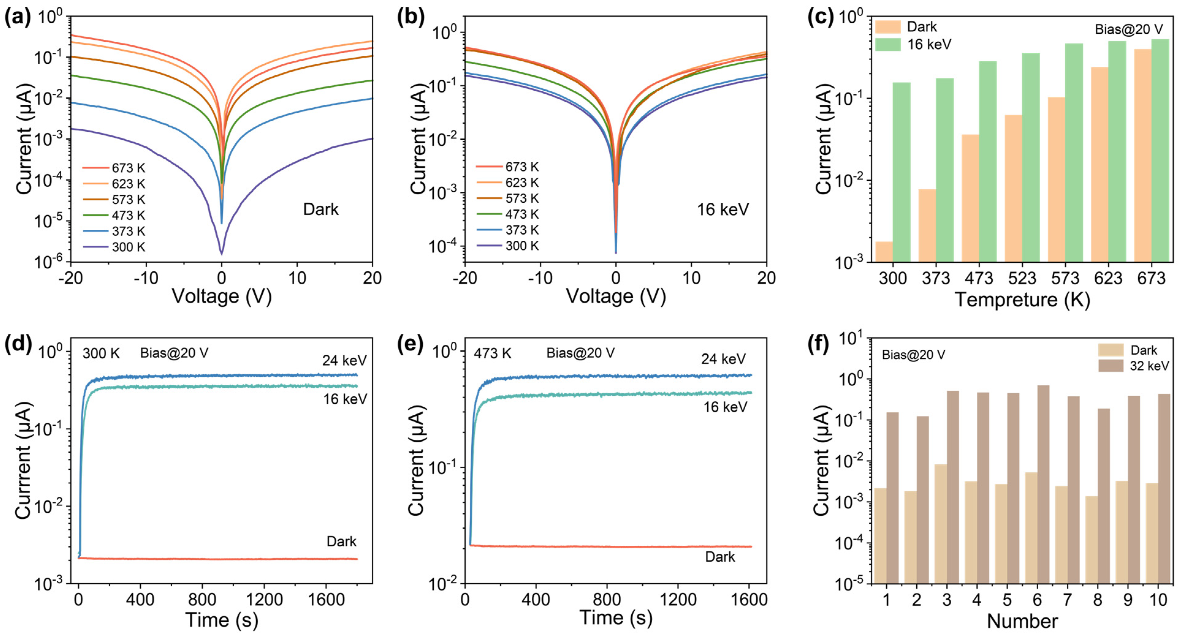
:
1. Introduction
2. Materials and Methods
2.1. Materials
2.2. Device Fabrication
2.3. Characterization
3. Results and Discussion
4. Conclusions
Author Contributions
Funding
Institutional Review Board Statement
Informed Consent Statement
Data Availability Statement
Conflicts of Interest
References
- Rowlands, J.A. Material change for X-ray detectors. Nature 2017, 550, 47–48. [Google Scholar] [CrossRef] [PubMed] [Green Version]
- Basirico, L.; Ciavatti, A.; Cramer, T.; Cosseddu, P.; Bonfiglio, A.; Fraboni, B. Direct X-ray photoconversion in flexible organic thin film devices operated below 1 V. Nat. Commun. 2016, 7, 13063. [Google Scholar] [CrossRef] [PubMed] [Green Version]
- Wei, H.; Fang, Y.; Mulligan, P.; Chuirazzi, W.; Fang, H.-H.; Wang, C.; Ecker, B.R.; Gao, Y.; Loi, M.A.; Cao, L. Sensitive X-ray detectors made of methylammonium lead tribromide perovskite single crystals. Nat. Photonics 2016, 10, 333–339. [Google Scholar] [CrossRef]
- Pan, W.; Yang, B.; Niu, G.; Xue, K.H.; Du, X.; Yin, L.; Zhang, M.; Wu, H.; Miao, X.S.; Tang, J. Hot-pressed CsPbBr3 quasi-monocrystalline film for sensitive direct X-ray detection. Adv. Mater. 2019, 31, 1904405. [Google Scholar] [CrossRef] [PubMed]
- Heiss, W.; Brabec, C. Perovskites target X-ray detection. Nat. Photonics 2016, 10, 288–289. [Google Scholar] [CrossRef]
- Chen, M.; Zhang, Z.; Zhan, R.; She, J.; Deng, S.; Xu, N.; Chen, J. Fast-response X-ray detector based on nanocrystalline Ga2O3 thin film prepared at room temperature. Appl. Surf. Sci. 2021, 554, 149619. [Google Scholar] [CrossRef]
- Zhou, F.; Li, Z.; Lan, W.; Wang, Q.; Ding, L.; Jin, Z. Halide Perovskite, a potential scintillator for X-ray detection. Small Methods 2020, 4, 2000506. [Google Scholar] [CrossRef]
- Reddy, P.S.; Kumar, R.A.R.; Mathews, M.G.; Amarendra, G. Remote Online Performance Evaluation of Photomultiplier Tube and Electronics of DPCAM. IEEE Trans. Nucl. Sci. 2017, 64, 2843–2853. [Google Scholar] [CrossRef]
- Li, Y.; Zha, G.; Guo, Y.; Xi, S.; Xu, L.; Jie, W. Investigation on X-ray photocurrent response of CdZnTe photon counting detectors. Sensors 2020, 20, 383. [Google Scholar] [CrossRef] [Green Version]
- Barbeau, P.; Collar, J.; Tench, O. Large-mass ultralow noise germanium detectors: Performance and applications in neutrino and astroparticle physics. J. Cosmol. Astropart. Phys. 2007, 2007, 009. [Google Scholar] [CrossRef]
- Li, X.; Meng, C.; Huang, B.; Yang, D.; Xu, X.; Zeng, H. All-Perovskite Integrated X-ray Detector with Ultrahigh Sensitivity. Adv. Opt. Mater. 2020, 8, 2000273. [Google Scholar] [CrossRef]
- Kasap, S.; Frey, J.B.; Belev, G.; Tousignant, O.; Mani, H.; Greenspan, J.; Laperriere, L.; Bubon, O.; Reznik, A.; DeCrescenzo, G. Amorphous and polycrystalline photoconductors for direct conversion flat panel X-ray image sensors. Sensors 2011, 11, 5112–5157. [Google Scholar] [CrossRef] [PubMed] [Green Version]
- Liang, H.; Cui, S.; Su, R.; Guan, P.; He, Y.; Yang, L.; Chen, L.; Zhang, Y.; Mei, Z.; Du, X. Flexible X-ray Detectors Based on Amorphous Ga2O3 Thin Films. ACS Photonics 2018, 6, 351–359. [Google Scholar] [CrossRef]
- Degheidy, A.R.; Elkenany, E.B.; Alfrnwani, O.A. Mechanical properties of AlPxSb1−x semiconductor alloys under the effect of temperature and pressure. Comput. Condens. Matter 2018, 16, e00310. [Google Scholar] [CrossRef]
- Duboz, J.-Y.; Lauegt, M.; Schenk, D.; Beaumont, B.; Reverchon, J.-L.; Wieck, A.D.; Zimmerling, T. GaN for X-ray detection. Appl. Phys. Lett. 2008, 92, 263501. [Google Scholar] [CrossRef]
- Lioliou, G.; Chan, H.; Gohil, T.; Vassilevski, K.; Wright, N.; Horsfall, A.; Barnett, A. 4H-SiC Schottky diode arrays for X-ray detection. Nucl. Instrum. Methods Phys. Res. Sect. A 2016, 840, 145–152. [Google Scholar] [CrossRef] [Green Version]
- Li, Z.; Chen, J.; Tang, H.; Zhu, Z.; Gu, M.; Xu, J.; Chen, L.; Ouyang, X.; Liu, B. Band gap engineering in β-Ga2O3 for a high-performance X-ray detector. ACS Appl. Electron. Mater. 2021, 3, 4630–4639. [Google Scholar] [CrossRef]
- Bohon, J.; Muller, E.; Smedley, J. Development of diamond-based X-ray detection for high-flux beamline diagnostics. J. Synchrotron Radiat. 2010, 17, 711–718. [Google Scholar] [CrossRef]
- Zhou, L.; Chen, L.; Ruan, J.; Lu, X.; Liu, B.; Gao, R.; Li, Y.; Geng, L.; Ouyang, X. Pulsed X-ray detector based on Fe doped β-Ga2O3 single crystal. J. Phys. D: Appl. Phys. 2021, 54, 274001. [Google Scholar] [CrossRef]
- Lioliou, G.; Whitaker, M.; Barnett, A. High temperature GaAs X-ray detectors. J. Appl. Phys. 2017, 122, 244506. [Google Scholar] [CrossRef] [Green Version]
- Yang, J.; Ahn, S.; Ren, F.; Pearton, S.; Jang, S.; Kim, J.; Kuramata, A. High reverse breakdown voltage Schottky rectifiers without edge termination on Ga2O3. Appl. Phys. Lett. 2017, 110, 192101. [Google Scholar] [CrossRef] [Green Version]
- Hou, X.; Zhao, X.; Zhang, Y.; Zhang, Z.; Liu, Y.; Qin, Y.; Tan, P.; Chen, C.; Yu, S.; Ding, M. High-performance harsh-environment-resistant GaOX solar-blind photodetectors via defect and doping engineering. Adv. Mater. 2022, 34, 2106923. [Google Scholar] [CrossRef] [PubMed]
- Li, S.; Yue, J.; Ji, X.; Lu, C.; Yan, Z.; Li, P.; Guo, D.; Wu, Z.; Tang, W. Oxygen vacancies modulating the photodetector performances in ε-Ga2O3 thin films. J. Mater. Chem. C 2021, 9, 5437–5444. [Google Scholar] [CrossRef]
- Ni, D.; Wang, Y.; Li, A.; Huang, L.; Tang, H.; Liu, B.; Cheng, C. ALD oxygen vacancy-rich amorphous Ga2O3 on three-dimensional urchin-like ZnO arrays for high-performance self-powered solar-blind photodetectors. Nanoscale 2022, 14, 3159–3165. [Google Scholar] [CrossRef] [PubMed]
- Chen, Y.; Lu, Y.; Yang, X.; Li, S.; Li, K.; Chen, X.; Xu, Z.; Zang, J.; Shan, C. Bandgap engineering of Gallium oxides by crystalline disorder. Mater. Today Phys. 2021, 18, 100369. [Google Scholar] [CrossRef]
- Zhang, Q.; Li, N.; Zhang, T.; Dong, D.; Yang, Y.; Wang, Y.; Dong, Z.; Shen, J.; Zhou, T.; Liang, Y.; et al. Enhanced gain and detectivity of unipolar barrier solar blind avalanche photodetector via lattice and band engineering. Nat. Commun. 2023, 14, 418. [Google Scholar] [CrossRef] [PubMed]
- Zhang, C.; Liu, K.; Ai, Q.; Sun, X.; Chen, X.; Yang, J.; Zhu, Y.; Cheng, Z.; Li, B.; Liu, L.; et al. High-performance fully transparent Ga2O3 solar-blind UV photodetector with the embedded indium–tin–oxide electrodes. Mater. Today Phys. 2023, 33, 101034. [Google Scholar] [CrossRef]
- Qin, Y.; Li, L.; Zhao, X.; Tompa, G.S.; Dong, H.; Jian, G.; He, Q.; Tan, P.; Hou, X.; Zhang, Z.; et al. Metal–Semiconductor–Metal ε-Ga2O3 Solar-Blind Photodetectors with a Record-High Responsivity Rejection Ratio and Their Gain Mechanism. ACS Photonics 2020, 7, 812–820. [Google Scholar] [CrossRef]
- Hany, I.; Yang, G.; Chung, C.-C. Fast X-ray detectors based on bulk β-Ga2O3 (Fe). J. Mater. Sci. 2020, 55, 9461–9469. [Google Scholar] [CrossRef]
- Lu, X.; Zhou, L.; Chen, L.; Ouyang, X.; Liu, B.; Xu, J.; Tang, H. Schottky X-ray detectors based on a bulk β-Ga2O3 substrate. Appl. Phys. Lett. 2018, 112, 103502. [Google Scholar] [CrossRef]
- Zhang, Z.; Chen, Z.; Chen, M.; Wang, K.; Chen, H.; Deng, S.; Wang, G.; Chen, J. ε-Ga2O3 Thin Film Avalanche Low-Energy X-ray Detectors for Highly Sensitive Detection and Fast-Response Applications. Adv. Mater. Technol. 2021, 6, 2001094. [Google Scholar] [CrossRef]
- Chen, J.; Tang, H.; Liu, B.; Zhu, Z.; Gu, M.; Zhang, Z.; Xu, Q.; Xu, J.; Zhou, L.; Chen, L.; et al. High-Performance X-ray Detector Based on Single-Crystal beta-Ga2O3: Mg. ACS Appl. Mater. Interfaces 2021, 13, 2879–2886. [Google Scholar] [CrossRef] [PubMed]
- Xie, C.; Lu, X.T.; Ma, M.R.; Tong, X.W.; Zhang, Z.X.; Wang, L.; Wu, C.Y.; Yang, W.H.; Luo, L.B. Catalyst-Free Vapor–Solid Deposition Growth of β-Ga2O3 Nanowires for DUV Photodetector and Image Sensor Application. Adv. Opt. Mater. 2019, 7, 1901257. [Google Scholar] [CrossRef]
- He, T.; Zhang, X.; Ding, X.; Sun, C.; Zhao, Y.; Yu, Q.; Ning, J.; Wang, R.; Yu, G.; Lu, S.; et al. Broadband Ultraviolet Photodetector Based on Vertical Ga2O3/GaN Nanowire Array with High Responsivity. Adv. Opt. Mater. 2019, 7, 1801563. [Google Scholar] [CrossRef]
- Li, G.; Zhang, K.; Wu, Y.; Wang, Q.; Pan, Z.; Fu, X.; Wang, L.; Feng, S.; Lu, W. Patterned Ga2O3 nanowires synthesized by CVD method for High-performance self-powered ultraviolet photodetector. J. Alloys Compd. 2023, 934, 168070. [Google Scholar] [CrossRef]
- Lu, Y.-C.; Zhang, Z.-F.; Yang, X.; He, G.-H.; Lin, C.-N.; Chen, X.-X.; Zang, J.-H.; Zhao, W.-B.; Chen, Y.-C.; Zhang, L.-L.; et al. High-performance solar-blind photodetector arrays constructed from Sn-doped Ga2O3 microwires via patterned electrodes. Nano Res. 2022, 15, 7631–7638. [Google Scholar] [CrossRef]
- Rao, R.; Rao, A.; Xu, B.; Dong, J.; Sharma, S.; Sunkara, M. Blueshifted Raman scattering and its correlation with the [110] growth direction in gallium oxide nanowires. J. Appl. Phys. 2005, 98, 094312. [Google Scholar] [CrossRef] [Green Version]
- Du, X.; Li, Z.; Luan, C.; Wang, W.; Wang, M.; Feng, X.; Xiao, H.; Ma, J. Preparation and characterization of Sn-doped β-Ga2O3 homoepitaxial films by MOCVD. J. Mater. Sci. 2015, 50, 3252–3257. [Google Scholar] [CrossRef]
- Kaur, D.; Kumar, M. A strategic review on gallium oxide based deep-ultraviolet photodetectors: Recent progress and future prospects. Adv. Opt. Mater. 2021, 9, 2002160. [Google Scholar] [CrossRef]
- Li, X.-X.; Zeng, G.; Li, Y.-C.; Zhang, H.; Ji, Z.-G.; Yang, Y.-G.; Luo, M.; Hu, W.-D.; Zhang, D.W.; Lu, H.-L. High responsivity and flexible deep-UV phototransistor based on Ta-doped β-Ga2O3. npj Flex. Electron. 2022, 6, 47. [Google Scholar] [CrossRef]
- Zhang, Z.; Lin, C.; Yang, X.; Tian, Y.; Gao, C.; Li, K.; Zang, J.; Yang, X.; Dong, L.; Shan, C. Solar-blind imaging based on 2-inch polycrystalline diamond photodetector linear array. Carbon 2021, 173, 427–432. [Google Scholar] [CrossRef]
- Li, K.; Yang, X.; Tian, Y.; Chen, Y.; Lin, C.; Zhang, Z.; Xu, Z.; Zang, J.; Shan, C. Ga2O3 solar-blind position-sensitive detectors. Sci. China-Phys. Mech. Astron. 2020, 63, 117312. [Google Scholar] [CrossRef]
- Gong, X.; Tong, M.; Xia, Y.; Cai, W.; Moon, J.S.; Cao, Y.; Yu, G.; Shieh, C.-L.; Nilsson, B.; Heeger, A.J. High-Detectivity Polymer Photodetectors with Spectral Response from 300 nm to 1450 nm. Science 2009, 325, 1665–1667. [Google Scholar] [CrossRef]
- Chen, Y.; Yang, X.; Zhang, Y.; Chen, X.; Sun, J.; Xu, Z.; Li, K.; Dong, L.; Shan, C. Ultra-sensitive flexible Ga2O3 solar-blind photodetector array realized via ultra-thin absorbing medium. Nano Res. 2021, 15, 3711–3719. [Google Scholar] [CrossRef]
- Chen, Y.; Yang, X.; Zhang, C.; He, G.; Chen, X.; Qiao, Q.; Zang, J.; Dou, W.; Sun, P.; Deng, Y.; et al. Ga2O3-Based Solar-Blind Position-Sensitive Detector for Noncontact Measurement and Optoelectronic Demodulation. Nano Lett. 2022, 22, 4888–4896. [Google Scholar] [CrossRef] [PubMed]
- Zhang, Z.; Chen, M.; Zhan, R.; Chen, H.; Wang, K.; Deng, S.; Chen, J. Fabrication of nanocrystalline Ga2O3-NiO heterojunctions for large-area low-dose X-ray imaging. Appl. Surf. Sci. 2022, 604, 154623. [Google Scholar] [CrossRef]
- Sorifi, S.; Moun, M.; Kaushik, S.; Singh, R. High-Temperature Performance of a GaSe Nanosheet-Based Broadband Photodetector. ACS Appl. Electron. Mater. 2020, 2, 670–676. [Google Scholar] [CrossRef]
- Zhao, B.; Wang, F.; Chen, H.; Wang, Y.; Jiang, M.; Fang, X.; Zhao, D. Solar-blind avalanche photodetector based on single ZnO–Ga2O3 core–shell microwire. Nano Lett. 2015, 15, 3988–3993. [Google Scholar] [CrossRef]
- Girolami, M.; Bosi, M.; Serpente, V.; Mastellone, M.; Seravalli, L.; Pettinato, S.; Salvatori, S.; Trucchi, D.M.; Fornari, R. Orthorhombic undoped κ-Ga2O3 epitaxial thin films for sensitive, fast, and stable direct X-ray detectors. J. Mater. Chem. C 2023, 11, 3759–3769. [Google Scholar] [CrossRef]


| Material | Idark(A) | R(A/W) @254 nm | Rise/Decay time (s) | Structure | Work Temperature | Reference |
|---|---|---|---|---|---|---|
| GaOX | ≈10−13 | 66.7 | 0.08/−@254 nm | MSM | 573 K | [22] |
| Ga2O3 | ≈10−12 | - | <0.3/<0.3@X-ray | MSM | - | [29] |
| Ga2O3 | ≈10−10 | - | 0.132/0.037@X-ray | MSM | - | [31] |
| Ga2O3 | ≈10−10 | - | <0.2/<0.2@X-ray | MSM | - | [32] |
| Ga2O3 MWs | ≈10−11 | 2409 | 0.0079/1.18@254 nm | MSM | - | [36] |
| Ga2O3 | 1.6 × 10⁻¹¹ | 295 | 1.7 × 10⁻⁶/1.1 × 10−4@254 nm | MSM | - | [44] |
| Ga2O3 | ≈10−9 | 0.0485 | 8 × 10⁻⁷/10−4@254 nm | MSM | - | [45] |
| Ga2O3/ZnO | 2.3 × 10⁻⁸ | 1300 | <2 × 10⁻⁵/4.2 × 10−5@254 nm | Heterostructure | - | [48] |
| Ga2O3 | ≈10−12 | - | <0.5/−@X-ray | MSM | - | [49] |
| Ga2O3 MWs | ≈10−9 | 1573 | 1.8 × 10⁻⁵/0.03@254 nm 43.4/22.3@X-ray | MSM | 623 K | This work |
Disclaimer/Publisher’s Note: The statements, opinions and data contained in all publications are solely those of the individual author(s) and contributor(s) and not of MDPI and/or the editor(s). MDPI and/or the editor(s) disclaim responsibility for any injury to people or property resulting from any ideas, methods, instructions or products referred to in the content. |
© 2023 by the authors. Licensee MDPI, Basel, Switzerland. This article is an open access article distributed under the terms and conditions of the Creative Commons Attribution (CC BY) license (https://creativecommons.org/licenses/by/4.0/).
Share and Cite
Zhang, C.; Dou, W.; Yang, X.; Zang, H.; Chen, Y.; Fan, W.; Wang, S.; Zhou, W.; Chen, X.; Shan, C. X-ray Detectors Based on Ga2O3 Microwires. Materials 2023, 16, 4742. https://doi.org/10.3390/ma16134742
Zhang C, Dou W, Yang X, Zang H, Chen Y, Fan W, Wang S, Zhou W, Chen X, Shan C. X-ray Detectors Based on Ga2O3 Microwires. Materials. 2023; 16(13):4742. https://doi.org/10.3390/ma16134742
Chicago/Turabian StyleZhang, Chongyang, Wenjie Dou, Xun Yang, Huaping Zang, Yancheng Chen, Wei Fan, Shaoyi Wang, Weimin Zhou, Xuexia Chen, and Chongxin Shan. 2023. "X-ray Detectors Based on Ga2O3 Microwires" Materials 16, no. 13: 4742. https://doi.org/10.3390/ma16134742