Abstract
There are two main ways of carrying out the electrical discharge machining of the insulating ceramics: changing the electrical and chemical properties of ceramics due to additives in producing composites/nanocomposites and changing the electrical and chemical properties in the interelectrode gap. This review summarizes and analyzes the current data on the machinability in water suspension and hydrocarbons depending on the electrical properties of the ceramic composites and assisting means such as coating and powder. There are provided the existing approaches and original methods for solving the global problem of the electrical discharge machining of insulating ceramics, suggesting further development of the existing methods since, up to now, the experimental research is non-systemic. The dependencies of the machinability on the electrical properties of conductive ceramic composites, the specific electrical resistance of the assisting coating, and the assisting powder’s band gap and concentration for machining insulating ceramics are revealed. The higher the electrical conductivity, the higher the machinability of ceramic composites, and the lower the band gap, the higher the machinability for insulating ceramics. Two technological gaps were revealed in the powder’s concentration that can be a particular case of logarithmic decrement of attenuation. The proposed approach suggests using assisting powder with the lower band gap.
1. Introduction
Electrical discharge machining (EDM) can be successfully applied to single-phase ceramics, cermets, and ceramic/matrix composites as long as they exhibit electrical resistivity lower than 100–300 Ω·cm [1,2]. Non-conductive ceramics such as
- most of the oxide ceramics (alumina Al2O3, aluminum nitride AlN, magnesium oxide MgO, zirconia ZrO2);
- some nitride ceramics (silicon nitride Si3N4, boron nitride BN);
- oxide-nitride ceramics such as SiAlON, a solid solution of silicon nitride (Si3N4), where Si–N bonds are partly replaced with Al–N and Al–O bonds do not meet the minimum requirement of an electrical conductivity of 10−2 Ω·cm to be subjected to electrical erosion [3,4,5,6,7,8,9] (Figure 1). However, due to their exceptional exploitation properties, they are of tremendous industrial interest for some critical applications. Secondary electrically conductive phases are incorporated to influence such insulating ceramics’ electrical conductivity [10,11]. Metal-like carbides, carbonitrides, and nitrides of some transition metals that form predominantly metallic bonds (TiC, Ti(CN), TiN) serve the conductive phases in electro-conductive ceramic composites and nanocomposites based on oxide, nitride, or oxide–nitride insulating ceramics [12,13]. Metal-like carbides exhibit electrical conductivity similar to metals. They are delocalized metal bond d-element carbides based on iron, tungsten, tantalum, titan, vanadium, niobium, chrome, molybdenum, and nickel, of IV–X element groups, excluding platinum-group metals with a low electronegativity of 1.36–2.3 of Pauling’s scale and, consequently, high metallic properties [14]. These measures improve their conductive properties, enabling them to be subjected to electrical discharge machining and wear-resistance properties to operate in friction pairs (for example, for cutting tools).

Figure 1.
Specific electrical resistance ρ of some ceramics (* provided for reference).
The existing techniques of electrical discharge machining insulating ceramics suggest two main methods (Figure 2):
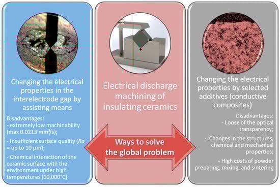
Figure 2.
Two main ways to solve the global problem of electrical discharge machining of insulating ceramics and their disadvantages.
- ○
- By changing the properties of ceramics due to additives selected following the electrical and chemical properties of components [15,16];
- ○
- By changing the electrical and chemical properties in the interelectrode gap [17,18].
The main disadvantage of the first method is the complete and expensive nanomodification of the material with the loss of such properties as optical transparency. The disadvantage of the second method is its low efficiency concerning insulating ceramics, associated with the above-described features. This work aims:
- To review the recent advances and developments in the electrical discharge machining of insulating ceramics;
- To summarize and analyze the current data on the machinability of conductive ceramic composites and the insulating ceramics based on oxides and nitrides in water suspension and hydrocarbons depending on the electrical properties of the ceramics and assisting means;
- To search the approaches and original methods for solving the global problem of the electrical discharge machining of insulating ceramics.
The proposed approach can be extended to develop solutions for electrical discharge machining other insulating materials (including ones filled with glass fiber).
2. Electrical Conductivity of Insulating Ceramics and Conductive Composites
Typical ceramics are chemical compounds based on polar bonding. The absence of slip planes makes them extremely brittle by comparison with, for example, steel. When ceramic pieces have been manufactured, they cannot be subjected to heat treatment to induce deliberate changes in their structure. Whereas steels possess a dense structure following crystallization and recrystallization, ceramics fundamentally constitute a multiphase system comprising crystals, a binder phase, and pores [19].
Natural electrical conduction by free lattice electrons makes some carbide, carbonitride, and nitride ceramics electrically conductive (delocalized metal bond d-element carbides of IV–X groups excluding platinum group metals). For insulating ceramics (mainly oxide ceramics and nitride ceramics of some elements of III–V groups such as AlN), two mechanisms are utilized to make engineering ceramics electrically conductive:
- Doping with conductive elements;
- Incorporating impurity atoms [20].
Electrically conductive carbides, carbonitrides, and nitrides serve as usual doping components to make insulating ceramics electrically conductive. These ceramics are primarily used as doping components because they are chemically neutral to oxygen. It should be noted that other nitrides mainly exhibit unstable chemically active and explosive properties (Cu3N, Mg3N2, Pb3N2, Zn3N2) and decomposes to oxides.
The electrical conductivity of oxide or nitride ceramic composites can be improved by combining the transition-metal carbide or nitride particles with the electrical conductivity of ρ = 102–106 µΩ·cm and the high strength and wear resistance of the matrix [21]. The improved high-performance ceramic matrix presents a fine-grained microstructure (Table 1) that does not deteriorate to operating temperatures close to 1000 °C. The Vickers hardness and fracture toughness of the composites increased with TiC phase addition into Al2O3-TiC composites containing 30 and 40 vol.% TiC. The composite with 40 vol.% TiC showed the highest flexural strength (687 ± 39 MPa), fracture toughness (7.8 ± 0.4 MPa·m1/2), and hardness (22.3 ± 0.3 GPa) with a homogeneous distribution of the second phase within the ceramic matrix [22]. The conductive properties mainly depend on conductive additives concentration [23] when the mechanical properties do not correlate with the content of the ceramic basis (Al2O3-content, Table 1).

Table 1.
Electrophysical and mechanical properties of Al2O3-based ceramics.
The conductors have specific electrical resistance ρ < 10−5 Ω·m as the specific electrical resistance of dielectrics is ρ > 10⁸ Ω·m. The value of specific electrical resistance for produced conductive ceramic with 30 vol.% of TiC is close to the value for carbon in the form of graphite (ρ = 8 × 10⁻⁶ Ω·m) [28]. Thus, the samples of sintered Al2O3 + TiC ceramic with more than 30 vol.% of TiC are suitable for electrical discharge machining [25,26,27]. The electrical conductivity of some conductors can fluctuate in the range of 10–10−12 S/m (ρ = 10−1–1012 Ω·m) and also depends on many factors, including temperature and crystal lattice orientation (some materials, such as carbon, exhibit anisotropy of electrical properties) [29,30,31].
The addition of carbon nanotubes (CNTs) to the zirconia matrix in zirconia-based composites induces a substantial increase in electrical conductivity associated primarily with the fact that zirconium and zirconium carbide formed because of the thermochemical reaction have similar electrical conductivity (Table 2) [24,32,33,34,35]. The formation of zirconium carbide occurs through the thermal dissociation of zirconium dioxide and the reduction of lower oxides with carbon:
where T1 and T2 are the subjects of a separate study.
Table 2.
Electrical properties of some Zr-containing materials.
Simultaneously, it provokes relatively slight thermal conductivity changes (Table 2). The specific electrical conductivity of amorphous oxide ceramics and semiconductors increases significantly with an increase in temperatures since the concentration and mobility of charge carriers are exponentially dependent on temperature (t, °C) as was approximated:
where σ0 is the value of specific electrical conductivity at normal temperature, and β is the temperature coefficient (1/°C). It can be presented as follows (Figure 3). As can be seen with ρ > 108 Ω·m and variable value β (for different materials), it is possible to achieve superconductivity conditions at the lowest and highest temperatures. The graphs for other types of dielectric and semiconductive oxide and nitride ceramics have similar trends and vary in σ0. For crystalline ceramics, the observed increase in specific and volumetric electrical conductivity is less pronounced, and for metals, it has the opposite tendency [24,39].
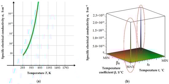
Figure 3.
Theoretical specific electrical conductivity σ for dielectric and semiconductive oxide and nitride ceramics (by the example of ZrO2): (a) with β = const, where t0 = +20 °C and σ0 = 10 S·m−1; (b) with the theoretically varied the temperature coefficient β, where t0 = +20 °C and σ0 = 10−8 S·m−1, extremes (marked red) may correspond to superconducting conditions.
An introduction of 30–40 vol. % TiNx (x is in the range of 0.6–1.2; electrical resistivity ρ at +20 °C of 1.0 × 10⁻⁷–4.0 × 10⁻⁷ Ω·m in bulk; 3.0 × 10⁻⁷–1.0 × 10⁻⁶ Ω·m by plasma vapor deposition (PVD); 2.0 × 10⁻⁶–1.0 × 10⁻⁴ Ω·m by chemical vapor deposition (CVD)) into Si3N4 (1.0 × 10⁴–1.0 × 10¹³ Ω·m) provides an electrically conductive composite with a decreased electrical resistivity of ~10−5 Ω·m. Introducing the conductive component also improves mechanical properties such as fracture toughness, strength, and wear resistance [40,41,42].
The problem with Al-based ceramics is in forming pyrophoric ionic salt-like carbides Al3C4 or Al2(C2)3 (yellow crystals), where Al3C4 is methanide with (C = C)4− and Al2(C2)3 is acetylenide with (C = C)2− that exhibit insulating properties as for Be2C, Li4C, Mg2C (C4−) or Ag2C2, CuC2, CaC2, Li2C2, BaC2 (C22−) unlike metal-like carbides (CrxCy, FexCy, MoxCy, NbxCy, NixCy, TaxCy, TiC, VxCy, WC). At a temperature of the thermal decomposition (dissociation), Al2O3 ceramics dissociate as follows [24,43]:
or
Electrical erosion of alumina in the absence of hydrocarbons can be accompanied by a chemical reaction of dissociated molecules that compose the following insoluble sediment, which decomposes when heated above 848 K:
A similar issue is related to the dissociation of AlN:
The released aluminum reacts with the carbon similarly to (5). It can hydrolyze slowly in water:
At the atmosphere, nanofilms of alumina with a thickness of several nanometers are formed at temperatures above 973 K, which can keep from hydrolysis to temperatures above 1643 K. Above this temperature, bulk oxidation occurs:
3. Advances in Electrical Discharge Machining of Ceramics
3.1. Electrical Discharge Machining of Conductive Ceramic Composites
The machinability of conductive ceramic composites in electrical discharge machining is presented in Table 3. A graphical presentation of the data compared with the maximal achievable machinability for the conductive materials (aluminum alloys, pure chrome, and copper) is shown in Figure 4.
Table 3.
Machinability of conductive ceramic composites in electrical discharge machining.
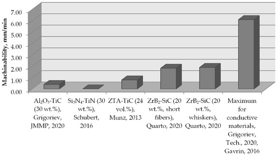
Figure 4.
The graphical presentation of conductive ceramic composites’ machinability via electrical discharge machining comparing with the maximal achievable machinability for the conductive materials, where Grigoriev, JMMP, 2020 [11], Schubert, 2016 [45], Munz, 2013 [46], Quarto, 2020 [47], Grigoriev, Tech., 2020 [48], Gavrin, 2016 [49].
In [26], it was shown that at 30 vol.% of TiC in Al2O3-TiC composite, the electrical conductivity corresponds to the adequate level that exceeds the percolation threshold, while Al2O3-TiC composite exhibits conductivity close to the conductivity of pure titanium at 40 vol.% of TiC. These types of ceramic composites have been known since the mid-1970s [29,30,31]. Still, many research groups conduct experiments on improving their properties by experimenting with technological factors and the dispersion of precursors.
The authors of [44] propose electrically conductive homogenous and dense SiAlON-TiN (10 wt.% and 20 wt.%) ceramic nanocomposite produced by advanced spark plasma sintering at 1700 °C suitable for wire electrical discharge machining. The nanocomposite with 20 wt.% TiN showed specific electrical resistance ρ lower than 1–3 Ω·m.
A. Schubert et al. experimentally investigated electrical discharge milling (ED milling) parameters of titanium nitride toughened silicon nitride (Si3N4-TiN) [45]. As Si3N4-TiN is decomposed at a high temperature in the discharge gap, it exhibits a particular ablation behavior that allows machining with a material removal rate of 200% compared to insulating ceramics of Al2O3-ZrO2 type. The maximum bore depth was 605 μm. The material removal rate was increased by increasing the power (Figure 5). A volume fraction of 30% of the conductive TiN phase is above the percolation threshold, and the electrical conductivity is provided by the TiN network [50]. For hot-pressed Si3N4-TiN (30vol.%), lowering the sintering temperature from 1700 to 1500 °C decreases resistivity from 0.18 to 0.004 Ω cm. The percolation threshold (Vc) is determined as follows:
where θ is a quantity of the conductive particles on the surface of the insulating ones; Di and dc are the diameters of the insulating and conductive particles. A higher diameter ratio (Di/dc) results in a lower Vc. The decomposition of the conductive ceramic composites unavoidably leads to a porous and foamy microstructure shown in [11] and correlates with analytic results of plasma chemistry [51]. During machining in oil, Si3N4-TiN decomposes on conductive carbides (TiC, SiC), and alumina–zirconia forms conductive ZrC [47] and non-conductive pyrotechnically active Al3C4 [52,53]. The formed Al3C4 can actively hamper processing by changing the discharge gap’s electrical conditions since hydrocarbon oil exhibits better electrical conductivity (1.9–4.3 Ω۔m depending on oil purity) than insulating ceramics (≤10−4 Ω۔m) [11].
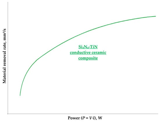
Figure 5.
The dependence of the machinability on power for Si3N4-TiN conductive ceramics in electrical discharge milling (logarithmic regression), based on [45].
M. Munz et al. [46] added TiC to zirconia and investigated the electrical discharge drilling of ZTA-TiC ceramics. They studied material removal rate, discharge energy, pulse shapes, peak current, and discharge time. They observed that the triangle pulse with a current of 20 A or less is better than the rectangle pulse for the electrical discharge drilling.
The suitable factors to accomplish the electrical discharge machining of conductive ceramic composites are the following:
- Assisting electrode is not required;
- Operational current of 0.05 A [26], 20 A or less [45];
- Operational voltage varies from 20 and 120 to 270 V [26];
- Frequency is 5 kHz;
- Discharge gap depends on the electrical conductivity of the workpiece material and is 10–200 µm.
3.2. Electrical Discharge Machining of Insulating Ceramics
D. Hanaoka et al. mentioned that the electrical conductivity limit was below 4 × 10⁻² S·m−1 [54]. The machining speed increases as the peak current and pulse width increase. The removal mechanism changes as the pulse width increases. As analyzed from the experiments, when the pulse width was set as 20–30 μs, the machining was stable, and a smoother machined surface was obtained. The pulse interval is not the dominant factor in increasing the machining speed but in improving the machined surface accuracy [55]. The material removal rate of Al2O3 and ZrO2 using adherent copper foil rose with an increase in peak current and pulse duration (Figure 6a). Additionally, the electrode wear rate of Al2O3 and ZrO2 increased with peak current but reduced with pulse duration [56]. However, when the pulse duration exceeded 200 μs, the tool wear rate during the Al2O3 ceramic machining demonstrated the reverse trend: the tool wear rate slightly increased at a pulse duration longer than 200 μs. The surface roughness of Al2O3 and ZrO2 increased with peak current and pulse duration (Figure 6b). Moreover, the surface roughness of the Al2O3 ceramic after electrical discharge machining was higher than for the ZrO2 ceramic at identical machining conditions that correlated with the plasma chemical nature of the processes between electrodes in the presence of heat higher than 3500 °C, which remained unexplained in the paper. The surface integrities of ZrO2 revealed more machining debris adhered to the machined surface, and the Al2O3 machined surface and thermal spalling features were rougher than for ZrO2. In general, the machining performance (material removal and tool wear rates) of ZrO2 with the copper adherent tape is better than Al2O3 with the same adherent. H. Zhang et al. [57] developed a technique to provide pulse generators with self-adapting voltage-adjusting for the electrical discharge machining of Al2O3 insulating ceramic. They demonstrated that the pulse generator could improve energy availability and discharge flexibility.
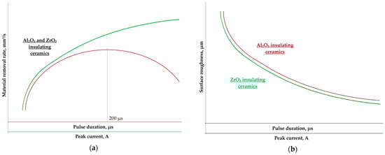
Figure 6.
The dependence of the machinability on peak current (logarithmic regression) and pulse duration (quadratic regression or exponential attenuation) (a); the dependence of the surface roughness on peak current and pulse duration (logarithmic regression) (b) for Al2O3 and ZrO2 insulating ceramics in electrical discharge machining, based on [56].
N. Ojha et al. [58] monitored the electrical signals when machining copper and non-conductive ceramic Si3N4. Voltage and current sparks’ signals were shown. They demonstrated that the most remarkable differences were a significant decrease for Si3N4 in the ringing behavior of the voltage signal and the absence of reverse current for Si3N4, and a decrease in the peak current value detected in the case of Si3N4. H. Gotoh et al. [59] used a unique technique for machining insulating ceramics Si3N4 with electrical discharge milling. They used a method in which the pulse discharge was longer than the pulse duration. Hence, the electrically conductive layer is created on the insulating ceramic surface, enabling machining.
The results of applying the assisting electrode technique primarily depend on the method of pre-coating the insulating ceramic workpiece and the main properties of the film (adhesion, thickness, chemical composition) (Table 4). The graphical presentation of the machinability of Al2O3 insulating ceramics is shown in Figure 7. As seen, the machinability in oil is 2.54 times higher than in water. From all the used assisting means, copper tape in combination with TiO2 powder provides higher machinability in the water-based dielectric medium. After processing, the film can be chemically removed from the ceramic surface with acetone, K2CrO4-H2SO4 mixture, or other solvents [60,61].
Table 4.
Types of assisting electrodes for electrical discharge machining of aluminum-containing insulating ceramics.
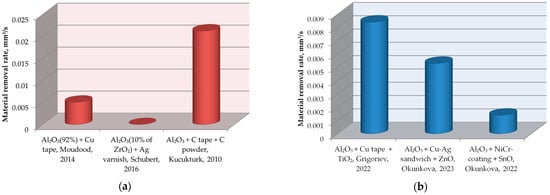
Figure 7.
The graphical presentation of Al2O3 insulating ceramic machinability via electrical discharge machining: (a) in hydrocarbons, (b) in water suspension, where Schubert, 2016 [45], Moudood, 2014 [63], Grigoriev, 2022 [65], Kucukturk, 2010 [66], Okunkova, 2023 [67], Okunkova, 2022 [68].
There are several types of coating to accomplish the process, such as copper assisting electrode [56,62,63,64,65], silver varnish [45,64], carbon conductive layer [66], multimaterial sandwich coatings [64,67], and Ni-Cr coating by plasma vapor deposition [68]. The assisting electrode made of copper tape can be removed easily from the AlN [64], Al2O3 [65], and ZrO2 [69] ceramic surface after the machining. There are also examples of electrical discharge machining of Si3N4 ceramics in TiO2 water-based suspension using conductive TiN coating deposited by plasma vapor deposition [70]. Any plasma vapor deposition coatings are difficult to remove after machining due to diffusion between the insulating workpiece and coating materials. However, the authors propose using assisting coating as a multifunctional one that provides conductive properties to the surface layer of the insulating workpiece and is used as a wear-resistant coating to prolongate the operational life of the Si3N4 ceramic cutting insert. In [66], it was experimentally shown that machinability strongly depends on electrical resistivity for TiO2, SiC, and ZrO2 ceramics during electrical discharge drilling when there is probably other nature (obviously, thermochemical combining with electrophysical) in Al2O3 and SiO2 ceramics machining, but the trends are similar.
The authors that research the electrical discharge machining of ZrO2 ceramics in hydrocarbon oil [56,66,71,72] report on forming conductive ZrC with the same conductivity as pure Zr [24]. Electrical discharge machining of aluminum-containing insulating ceramics in oil presents an unsolved scientific problem related to the high electronegativity of aluminum, which is very active towards oxygen and forms non-conductive carbides in its absence that are mistakenly named pyrolitic carbon. In [66], it was reported that not only “pyrolytic carbon” was identified in the working area.
A typical crater-like surface was detected during the electrical discharge machining of ZrO2 ceramics [45]. Thermal cracks and cleavages characterize the AlN ceramic surface [64]. The Al2O3 ceramic surface [68] is characterized by the traces of the thermal sublimation and drop-like deposition of the secondary structure of the compositions of secondary order formed by the products of the interaction of the decomposition of ceramics, assisting powder and dielectric medium.
The authors [64] consider chemical and plasma vapor deposition methods to be time-consuming and require costly equipment compared with the technique of AlN ceramics coating with the labor-intensive two-layered Ag sandwich coating with Ag nanoparticles between them additionally covered with copper tape. However, the PVD technique has demonstrated impressive results with a material removal rate of 0.0014 mm3/s in machining Al2O3 ceramics [68], which is more than two times higher than 0.006 mm3/s for AlN ceramics [64]. The actual problem of any plasma deposition technique of copper and silver coating is related to droplet formation [73,74] and coating low adhesion to insulating ceramics with a coating thickness above 3–4 µm [75,76]. At the same time, there is a global problem of discharge impulse reinitiating in the working zone when most of the coating is sublimated and decomposed in the dielectric medium. In this context, the Ni-Cr coating [68] has shown better prospects: it has smoother surface characterization when deposited on the insulating ceramic surface, exhibits better adhesion at the coating thickness up to 15 µm, and it can form intermetallic compounds of AlxNiy type (when x = 1, 3, … and y = 1, 3, …) [77] during coating sublimation and decomposition. These types of compounds exhibit superconductive properties and have prospects for future development. It should be noted that the addition of silver nanoparticles in the concentration of 0.1 g/L at the working zone fundamentally changes the electrical condition in the interelectrode gap [64]. It improves the material removal rate by ~6 times compared to triple copper tape and by ~30 times compared to silver double coating sandwich with Ag nanopowder.
The authors of [66] noticed that the programmed depth faster was achieved with a thicker conductive layer in a hydrocarbon medium. However, the authors reported that they did not understand the processes’ chemical nature during the electrical discharge machining of Al2O3 and ZrO2 ceramics, which needs additional research and explanation from the thermo- and electrochemistry point of view.
It is noticed that during electrical discharge machining of Si3N4 insulating ceramics, carbon-containing substances of the kerosene under high temperatures are often cracked and stuck to the positive pole in the voltage field [17]. The electrically conductive material adhered to the insulating workpiece’s surface during the electrical discharge machining of Si3N4, ZrO2 in kerosene. It consisted of decomposable carbon-containing substances from the fluid that can be conductive carbides of the ZrC group and semiconductive SiC adhered to the insulating workpiece surface. An electrically conductive carbide layer was formed during continuously generated electrical discharges. Thus, insulating ceramics are transformed into electrically machinable material during electrical discharge machining. However, during the electrical discharge machining of the sintered Al2O3 + 20% of ZrO2 stabilized with 3.9% of Y2O3 in kerosene, the conductive layer was not specified [78], obviously due to the known insulating properties of Al3C4. The eroded layer was removed mechanically after electrical discharge machining.
A standard silver varnish with 45% silver content was used to create the conductive layer of approximately 20 μm on the surface of ZrO2 ceramics [71]. After drying, the layer formation’s uniformity was tested by measuring the resistance using a Fluke multimeter. When the first layer was machined, a conducting rebuilt layer was generated on the workpiece, visible as black surface areas. The detailed composition of this layer was not under investigation. Still, it can be proposed that due to the thermal decomposition of the hydrocarbon oil by the electrical discharges and following plasma channel, ZrC was formed.
With an assisting electrode applied by a screen printing when electrical discharge machining of a semi-conductive silicon carbide [79] that did not exhibit electrical conductivity, the process was initially unstable, and it required the adjustment of machining factors such as current and frequency and tool geometry. The authors found that the cause of unstable machining might be the excessive generation of carbonized products. The average thickness of the carbonized layer on the ceramic surface was 24 µm with a standard deviation of 1.6 µm. The adaptation of tool geometry was produced to improve flushing in the working area. The maximum machined depth was 420 µm. The maximum material removal rate was 3.58 × 10⁻³ mm3/min (~0.215 mm3/s). Detached microstructures with an aspect ratio of 30 are machined. The present material removal mechanism was indicated as thermally induced spalling. No heat-affected zone was detected. The same group of researchers studied the electrical discharge machining of SiC-based composites [80]. The assisting electrode was generated from the decomposed dielectric oil and deposited on the ceramic surface. It is found that the conductivity of the SiC-based materials does not influence the machinability of ceramics’ microtexturing.
The suitable factors to accomplish the electrical discharge machining of insulating ceramics are the following:
- Assisting electrode material—copper tape/foil, silver coating/varnish, carbon tape, Cu + Ag sandwich, Ni + Cr PVD-coating;
- Assisting electrode thickness—from 12 to 300 µm;
- Type of assisting electrode deposition—adhesive, diffusion;
- Assisting powder material—Ag nanoparticles, graphite, SnO, TiO2, ZnO;
- Assisting powder granule size—from nano size to 10–30 µm in diameter;
- Assisting powder concentration for suspension of 0.1–150 g/L;
- Operational current of 0.3–0.4 A;
- Operational voltage of 108 V;
- The frequency of 2, 5, 7, 10, 30 kHz;
- Pulse duration of 0.5–2.5 µs;
- The discharge gap of 48–60 µm.
4. Discussion
Let us represent the summarized data on machinability via EDM presented in Table 3 and Table 4 in the form of graphs to approximate the obtained graphs up to the closest functions and analyze the revealed dependencies.
The dependence of conductive ceramic composites’ machinability via electrical discharge machining on electrical conductivity for some conductive ceramic composites based on Table 3 is presented in Figure 8. As can be seen, the dependence has a character of the logarithmic regression with a coefficient of determination of 0.7066:
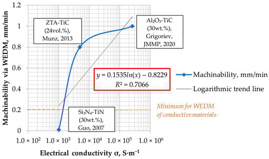
Figure 8.
The dependence of conductive ceramic composites’ machinability via wire electrical discharge machining on electrical conductivity, where R2 is a coefficient of determination, Grigoriev, JMMP, 2020 [11], Munz, 2013 [46], Guo, 2007 [50].
The higher the electrical conductivity, the higher the machinability.
Figure 9 presents graphs based on data from Table 4 depending on the specific resistance of the assisting coatings, the band gap, and the concentration of the assisting powder. The data are provided for Al2O3 and AlN ceramics. As it is seen in Figure 9a, the material removal rate is in inverse relationship with the specific resistance of the assisting coatings, and it is evident that despite the conviction of many authors that it is the electrical properties of the assisting coating that play a key role in the machinability of insulating ceramics. There should be the influence of other factors previously overlooked by the authors when developing a research plan and selecting an assisting electrode material. Figure 9b demonstrates the exponential relationship between the material removal rate and the band gap of the assisting powder for Al2O3 ceramics machined in hydrocarbons and water suspension (as more band gap is, as more dielectric properties exhibit material, up to 3–4 eV for semiconductors and more than 4–5 eV for dielectrics). Thus, the machinability dependence on the assisting powder’s electrical properties is proven:
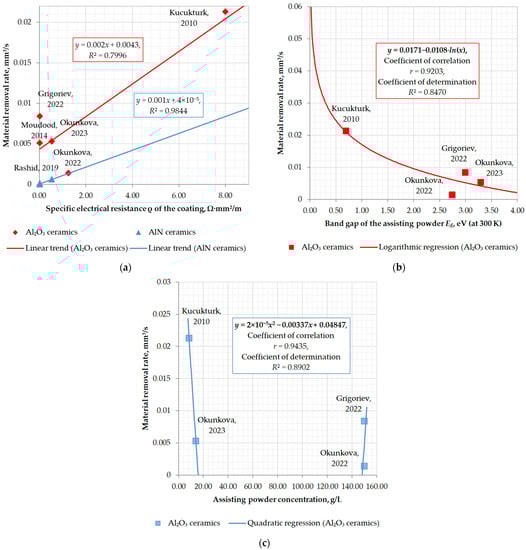
Figure 9.
The graphical presentation of Al-containing insulating ceramic machinability via electrical discharge machining: (a) dependence on the specific electrical resistance of the assisting coating; (b) dependence on the band gap of the assisting powder; (c) dependence on the assisting powder concentration, where Moudood, 2014 [63], Rashid, 2019 [64], Grigoriev, 2022 [65], Kucukturk, 2010 [66], Okunkova, 2023 [67], Okunkova, 2022 [68].
The lower the band gap, the higher the machinability.
The graph presents the results of the approximation. That is a logarithmic regression of the following type:
where a and b are empirical coefficients and require additional research. The data presented in Figure 9c are correlated with the data obtained in [65,67], where the assisting powder concentration influence on the material removal rate was researched in the concentration gap of 50–150 g/L and 7–100 g/L, correspondingly. The most pronounced results were achieved at 14 and 150 g/L. The reduction in machinability was observed in the range of the powder concentration from 21 to 100 g/L. The dependence corresponds to the quadratic regression as follows:
and can be a part of the logarithmic decrement of attenuation of the following type:
that seems more relevant to the mathematical expression of physical phenomena and requires more study.
For further development, it should be noted that TiO2 and ZnO are semiconductive with a band gap of 3.00–3.26 eV for TiO2 depending on its form (for anatase is more than for rutile) and ~3.37 eV for ZnO. It can be quite a perspective to consider adding other semiconductors with lower band gap values to improve conductivity conditions in the interelectrode gap. However, most of them as Cd3As2, Cd3P2, SnTe, VO2, Zn3P2 (the band gap of ~0, 0.5, 0.18, 0.7, 1.5 eV correspondingly [81,82,83,84,85]) are highly poisonous (4 points for health by NFPA 704). This excludes any possibility of their development and uses in the conditions of real production in the future. However, two of them deserve attention for further consideration—copper sulfides (CuxSy) and rare Tin(II) sulfide (α-SnS) with band energies of ~1.2 and 1.0–1.3 eV, correspondingly. They are available on the market in powder form.
Solving the problems of electrical discharge machining application techniques for aluminum-containing ceramics is of fundamental importance for science and applications such as electric power, the space industry, optics, and a promising cutting tool made of cutting ceramics. The development of superhard and highly wear- and heat-resistant materials based on ceramics with
- ○
- A low coefficient of linear thermal expansion (α × 106 of 7.0–8.0 K−1 for Al2O3, 4.0–6.0 K−1 for AlN, 3.0 K−1 for SiAlON at 20–1000 °C);
- ○
- Low thermal conductivity at normal temperatures (λ of 22–25 W·(m·K)−1 for Al2O3, > 170 W·(m·K)−1 for AlN, 85 W·(m·K)−1 for SiAlON at 20–100 °C); and
- ○
- Excellent optical properties (spectral transmission range of 0.17–5.5 µm for Al2O3, 0.2–5.0 µm for thin films of AlN [86], 2.5–5.0 for SiAlON [87]) by volumetric shaping will make it possible to create a group of new classes of metal-cutting tools with exceptional exploitation properties.
These tools can be aimed at machining high-entropy alloys, such as nickel- and titanium-based alloys achieving 800–1000 °C in the contact zone in friction pair [70,88], and carry out the sixth technological transition associated with Kondratieff’s waves [89,90].
The better results for the electrical discharge machining of insulating ceramics using assisting means can be summarized as follows (Table 5).
Table 5.
The summarized results of electrical discharge machining of insulating ceramics.
5. Conclusions
The conducted review allowed the recent advances in the electrical discharge machining of insulating ceramics to be summarized and analyzed, and revealed the dependences of the machinability on:
- ○
- The electrical properties of the ceramics for conductive ceramic composites (logarithmic regression);
- ○
- The specific electrical resistance of the assisting coating (needs additional research), the band gap (logarithmic regression) and the powder concentration of the assisting powder (quadratic regression) for insulating ceramics.
It has been shown that the lower the band gap, the higher the machinability. There are summarized data on electrical discharge machining factors for conductive ceramic composites and insulating ceramics.
The proposed approach of using the semiconductive powder composition with the small band gap can be extended to develop solutions for electrical discharge machining other insulating materials.
The electrical discharge machining of insulating ceramics has vast potential. It requires transitioning from laboratory conditions to real industrial applications to process reinforcing ceramics and other new ceramic-based composites to produce:
- A novel helical cutting tool with exploitation properties that can be of a critical advantage in milling new nickel- and titan-based and superalloys above 800 °C close to or even exceeding the properties of the pure sintered oxide and nitride ceramics;
- A new nanocomposite with physical properties that exceed the properties of the known materials in electrical resistivity, hot hardness, resistance to abrasive wear, linear thermal expansion, and thermal conductivity that can be not available to be shaped by traditional milling and turning due to their exceptional properties for aerospace applications.
The existing technological approaches in electrical discharge machining insulating ceramics have no advantages or disadvantages. The technology itself is not suitable for machining insulating materials and, by the existing logic, should not provide any results. However, some researchers put their efforts into exploring the limits of the existing technology of electrical discharge machining without putting any mechanical effort on the surface of the insulating materials using special measures such as providing an electrically conductive layer on the surface of the insulating ceramics. The machining is performed using the thermal effect of the electrical discharges, providing conductive particles and/or debris in the discharge gap to make the discharges denser and changing the electrical conditions in the interelectrode gap. The most outstanding in this context is the fact that many research groups achieve the machinability of the insulating ceramics by electrical discharge machining that is much less than for the convenient conductive materials but still shows impressive data (up to 0.0051–0.0213 mm3/s).
Author Contributions
Conceptualization, S.N.G.; methodology, M.A.V.; software, A.A.O.; validation, M.A.V.; formal analysis, A.A.O.; investigation, A.A.O.; resources, M.A.V.; data curation, M.A.V.; writing—original draft preparation, A.A.O.; writing—review and editing, M.A.V.; visualization, A.A.O.; supervision, S.N.G.; project administration, S.N.G.; funding acquisition, S.N.G. All authors have read and agreed to the published version of the manuscript.
Funding
This work was supported financially by the Ministry of Science and Higher Education of the Russian Federation (project No. FSFS-2021-0003).
Institutional Review Board Statement
Not applicable.
Informed Consent Statement
Not applicable.
Data Availability Statement
Data are available in a publicly accessible repository.
Acknowledgments
This study was carried out on the equipment of the Center of collective use of MSUT “STANKIN” supported by the Ministry of Higher Education of the Russian Federation (project No. 075-15-2021-695 from 26 July 2021, unique identifier RF 2296.61321 × 0013).
Conflicts of Interest
The authors declare no conflict of interest.
References
- Grigoriev, S.N.; Nadykto, A.B.; Volosova, M.A.; Zelensky, A.A.; Pivkin, P.M. WEDM as a Replacement for Grinding in Machining Ceramic Al2O3-TiC Cutting Inserts. Metals 2021, 11, 882. [Google Scholar]
- Bocharov, G.S.; Eletskii, A.V.; Knizhnik, A.A. Nonlinear resistance of polymer composites with carbon nanotube additives in the percolation state. Tech. Phys. 2016, 61, 1506–1510. [Google Scholar] [CrossRef]
- Zholnin, A.G.; Tenishev, A.V.; Stolyarov, V.V. Effect of the Thermomechanical Compacting Conditions on the Electrical Conductivity of an Al2O3/Graphene Composite Material. Russ. Metall. 2019, 10, 1009–1014. [Google Scholar] [CrossRef]
- Karpov, A.V.; Konovalikhin, S.V.; Borovinskaya, I.P.; Sachkova, N.V.; Kovalev, D.Y.; Sytschev, A.E. Conductive TiB2-AlN-BN-Based Composite SHS Ceramics. Russ. J. Non-Ferr. Met. 2018, 59, 658–663. [Google Scholar]
- Melnik, Y.A.; Kozochkin, M.P.; Porvatov, A.N.; Okunkova, A.A. On Adaptive Control for Electrical Discharge Machining Using Vibroacoustic Emission. Technologies 2018, 6, 96. [Google Scholar] [CrossRef]
- Lukianova, O.A.; Khmara, A.N.; Perevislov, S.N.; Kolesnikov, D.A.; Krasilnikov, V.V. Electrical resistivity of silicon nitride produced by various methods. Ceram. Int. 2019, 45, 9497–9501. [Google Scholar]
- Rumiantseva, Y.Y.; Romanko, L.O.; Chasnyk, D.V.; Turkevich, V.Z.; Bushlya, V.M.; Fesenko, I.P.; Kaidash, O.M.; Chasnyk, V.I.; Rukin, V.P. Electrical Characteristics of Thermobarically Sintered cBN-NbN Composite. J. Superhard Mater. 2020, 42, 126–128. [Google Scholar]
- Vellaikal, M.; Kingon, A.I. Electrical and microstructural characterization of lead titanate thin films deposited by metal-organic chemical vapor deposition onto platinum and magnesium oxide. Thin Solid Film. 1996, 287, 139–145. [Google Scholar] [CrossRef]
- Kang, T.K.; Kim, S.J. Variations in The Electrical-Resistivity of Y2O3-Doped ZrO2 Ceramics with Microstructural Design. J. Phys. Condens. Matter 1994, 6, 4343–4350. [Google Scholar]
- Jiang, Y.; Wu, L.; Sun, W.Z. Influence of Sintering Additives and TiC on Properties of TiC/Si3N4 Ceramics. Powders Grains 2013, 1542, 125–128. [Google Scholar]
- Grigoriev, S.N.; Volosova, M.A.; Okunkova, A.A.; Fedorov, S.V.; Hamdy, K.; Podrabinnik, P.A.; Pivkin, P.M.; Kozochkin, M.P.; Porvatov, A.N. Electrical Discharge Machining of Oxide Nanocomposite: Nanomodification of Surface and Subsurface Layers. J. Manuf. Mater. Process. 2020, 4, 96. [Google Scholar]
- Lengauer, W.; Binder, S.; Aigner, K.; Ettmayer, P.; Guillou, A.; Debuigne, J.; Groboth, G. Solid-State Properties of Group IVB Carbonitrides. J. Alloys Compd. 1995, 217, 137–147. [Google Scholar]
- Shahzad, F.; Iqbal, A.; Kim, H.; Koo, C.M. 2D Transition Metal Carbides (MXenes): Applications as an Electrically Conducting Material. Adv. Mater. 2020, 32, 2002159. [Google Scholar]
- Tantardini, C.; Oganov, A.R. Thermochemical electronegativities of the elements. Communications 2021, 12, 2087. [Google Scholar] [CrossRef] [PubMed]
- Selvarajan, L.; Sathiya Narayanan, C.; Jeyapaul, R.; Manohar, M. Optimization of EDM process parameters in machining Si3N4-TiN conductive ceramic composites to improve form and orientation tolerances. Meas. J. Int. Meas. Confed. 2016, 92, 114–129. [Google Scholar]
- Lazar, I.; Majchrowski, A.; Soszyński, A.; Roleder, K. Phase Transitions and Local Polarity above TC in a PbZr0.87Ti0.13O3 Single Crystal. Crystals 2020, 10, 286. [Google Scholar]
- Deng, G.Q.; Guo, Y.F.; Peng, Q.J.; Lu, Z.S.; Bai, J.C. A Novel Discharging Status Distinguish Method on Machining Si3N4 by HS-WEDM. In Proceedings of the 16th International Symposium on Electromachining, ISEM 2010, Shanghai, China, 19–23 April 2010; pp. 275–278. [Google Scholar]
- Fukuzawa, Y.; Tani, T.; Mohri, N. Machining characteristics of insulated Si3N4 ceramics by electrical discharge method—Use of powder-mixed machining fluid. J. Ceram. Soc. Jpn. 2000, 108, 184–190. [Google Scholar] [CrossRef][Green Version]
- Volosova, M.; Okunkova, A.; Peretyagin, P.; Melnik, Y.A.; Kapustina, N. On Electrical Discharge Machining of Non-Conductive Ceramics: A Review. Technologies 2019, 7, 55. [Google Scholar]
- Tian, X.; Zhao, J.; Wang, Y.; Gong, F.; Qin, W.; Pan, H. Fabrication and mechanical properties of Si3N4/(W, Ti)C/Co graded nano-composite ceramic tool materials. Ceram. Int. 2015, 41, 3381–3389. [Google Scholar]
- Habib, S.S. Study of the parameters in electrical discharge machining through response surface methodology approach. Appl. Math. Model. 2009, 33, 4397–4407. [Google Scholar]
- Cheng, M.; Liu, H.; Zhao, B.; Huang, C.; Yao, P.; Wang, B. Mechanical properties of two types of Al2O3/TiC ceramic cutting tool material at room and elevated temperatures. Ceram. Int. 2017, 43, 13869–13874. [Google Scholar] [CrossRef]
- Wang, D.; Xue, C.; Cao, Y.; Zhao, J. Fabrication and cutting performance of an Al2O3/TiC/TiN ceramic cutting tool in turning of an ultra-high-strength steel. Int. J. Adv. Manuf. Technol. 2017, 91, 1967–1976. [Google Scholar] [CrossRef]
- Volosova, M.A.; Okunkova, A.A.; Fedorov, S.V.; Hamdy, K.; Mikhailova, M.A. Electrical Discharge Machining Non-Conductive Ceramics: Combination of Materials. Technologies 2020, 8, 32. [Google Scholar]
- Gevorkyan, E.; Rucki, M.; Panchenko, S.; Sofronov, D.; Chałko, L.; Mazur, T. Effect of SiC Addition to Al2O3 Ceramics Used in Cutting Tools. Materials 2020, 13, 5195. [Google Scholar] [CrossRef] [PubMed]
- Grigoriev, S.N.; Volosova, M.A.; Peretyagin, P.Y.; Seleznev, A.E.; Okunkova, A.A.; Smirnov, A. The Effect of TiC Additive on Mechanical and Electrical Properties of Al2O3 Ceramic. Appl. Sci. 2018, 8, 2385. [Google Scholar] [CrossRef]
- Sevidova, E.K.; Pupan, L.I.; Tsyuryupa, V.N. Influence of Coatings on the Surface Strength of Rapid Prototyping Products. Surf. Eng. Appl. Electrochem. 2008, 44, 367–369. [Google Scholar] [CrossRef]
- Cui, H.; Chen, Z.; Xiao, G.; Ji, L.; Yi, M.; Zhang, J.; Zhou, T.; Xu, C. Mechanical Properties and Microstructures of Al2O3/TiC/TiB2 Ceramic Tool Material. Crystals 2021, 11, 637. [Google Scholar] [CrossRef]
- Wahi, R.P.; Ilschner, B. Fracture-Behavior of Composites Based on Al2O3-TiC. J. Mater. Sci. 1980, 15, 875–885. [Google Scholar] [CrossRef]
- Watanabe, M.; Fukuura, I. Strength Of Al2O3 and Al2O3-TiC Ceramics in Relation to Their Fracture Sources. Am. Ceram. Soc. Bull. 1981, 60, 394. [Google Scholar]
- Movchan, B.A.; Grechanyuk, N.I. Microhardness And Microbrittleness of Condensates of the TiC- Al2O3 System. Inorg. Mater. 1981, 17, 972–973. [Google Scholar]
- Verdi, C.; Karsai, F.; Liu, P.T.; Jinnouchi, R.; Kresse, G. Thermal transport and phase transitions of zirconia by on-the-fly machine-learned interatomic potentials. NPJ Comput. Mater. 2021, 7, 156. [Google Scholar] [CrossRef]
- Borik, M.A.; Volkova, T.V.; Kulebyakin, A.V.; Kuritsyna, I.E.; Lomonova, E.E.; Myzina, V.A.; Milovich, F.O.; Ryabochkina, P.A.; Tabachkova, N.Y.; Zentsova, A.I.; et al. Thermal Conductivity of Cubic ZrO2 Single Crystals Stabilized with Yttrium Oxide. Phys. Solid State 2020, 62, 235–239. [Google Scholar] [CrossRef]
- Liu, D.M.; Tuan, W.H. Microstructure and its influence on thermal and electrical conductivity of ZrO2-Ag composites. Mater. Chem. Phys. 1997, 48, 258–262. [Google Scholar] [CrossRef]
- Melk, L.; Antti, M.L.; Anglada, M. Material removal mechanisms by EDM of Zirconia reinforced MWCNT nanocomposites. Ceram. Int. 2016, 42, 5792–5801. [Google Scholar] [CrossRef]
- Tu, R.; Xiao, B.; Zhang, S.; Deng, Z.; Li, Q.Z.; Yang, M.J.; Goto, T.; Zhang, L.M.; Ohmori, H. Mechanical, electrical and thermal properties of ZrC-ZrB2-SiC ternary eutectic composites prepared by arc melting. J. Eur. Ceram. Soc. 2018, 38, 3759–3766. [Google Scholar] [CrossRef]
- Dewi, A.K.; Yamaguchi, S.; Onitzuka, T.; Uno, M. Thermal conductivity calculation of ZrC-ZrO2 pellet from powder metallurgy as the surrogate of UCO kernel fuel. J. Nucl. Mater. 2020, 539, 152343. [Google Scholar] [CrossRef]
- Uporov, S.; Bykov, V.; Estemirova, S. Electrical and thermal conductivities of rapidly crystallized Cu-Zr alloys: The effect of anharmonicity. Phys. B-Condens. Matter 2016, 499, 97–106. [Google Scholar] [CrossRef]
- Gao, L.; Guan, R.; Zhang, S.; Zhi, H.; Jin, C.; Jin, L.; Wei, Y.; Wang, J. As-Sintered Manganese-Stabilized Zirconia Ceramics with Excellent Electrical Conductivity. Crystals 2022, 12, 620. [Google Scholar] [CrossRef]
- Boskovic, S.; Sigulinski, F.; Zivkovic, L. Liquid-phase sintering and properties of Si3N4-TiN composites. J. Mater. Synth. Process. 1999, 7, 119–126. [Google Scholar] [CrossRef]
- Zhang, S.H.; Kang, Z.Q.; Lu, Q. Room-temperature electrical conductivity property of Si3N4/TiN composite ceramics. Adv. Mater. Res. 2011, 150, 257–261. [Google Scholar]
- Xu, J.H.; Gu, M.Y.; Li, G.Y.; Jin, Y.P. Microstructures and properties of Si3N4/TiN ceramic nano-multilayer films. Trans. Nonferrous Met. Soc. China 1999, 9, 764–767. [Google Scholar]
- L’vov, B.V. Thermal Decomposition of Solids and Melts New Thermochemical Approach to the Mechanism, Kinetics and Methodology; Springer Science & Business Media: Berlin/Heidelberg, Germany, 2007; ISBN 978-1-4020-5672-7. [Google Scholar]
- Grigoriev, S.; Pristinskiy, Y.; Volosova, M.; Fedorov, S.; Okunkova, A.; Peretyagin, P.; Smirnov, A. Wire Electrical Discharge Machining, Mechanical and Tribological Performance of TiN Reinforced Multiscale SiAlON Ceramic Composites Fabricated by Spark Plasma Sintering. Appl. Sci. 2021, 11, 657. [Google Scholar] [CrossRef]
- Schubert, A.; Zeidler, H.; Kühn, R.; Hackert-Oschätzchen, M.; Flemmig, S.; Treffkorn, N. Investigation of Ablation Behaviour in Micro-EDM of Nonconductive Ceramic Composites ATZ and Si3N4-TiN. Procedia CIRP 2016, 42, 727–732. [Google Scholar] [CrossRef]
- Munz, M.; Risto, M.; Haas, R.; Landfried, R.; Kern, F.; Gadow, R. Machinability of ZTA-TiC ceramics by electrical discharge drilling. Procedia CIRP 2013, 6, 77–82. [Google Scholar] [CrossRef]
- Quarto, M.; Bissacco, G.; D’Urso, G. Study on ZrB2-Based Ceramics Reinforced with SiC Fibers or Whiskers Machined by Micro-Electrical Discharge Machining. Micromachines 2020, 11, 959. [Google Scholar] [CrossRef]
- Grigoriev, S.N.; Volosova, M.A.; Okunkova, A.A.; Fedorov, S.V.; Hamdy, K.; Podrabinnik, P.A.; Pivkin, P.M.; Kozochkin, M.P.; Porvatov, A.N. Wire Tool Electrode Behavior and Wear under Discharge Pulses. Technologies 2020, 8, 49. [Google Scholar] [CrossRef]
- Gavrin, V.N.; Kozlova, Y.P.; Veretenkin, E.P.; Logachev, A.V.; Logacheva, A.I.; Lednev, I.S.; Okunkova, A.A. Reactor target from metal chromium for “pure” high-intensive artificial neutrino source. Phys. Part. Nucl. Lett. 2016, 13, 267–273. [Google Scholar] [CrossRef]
- Guo, Z.; Blugan, G.; Kirchner, R.L.; Reece, M.; Graule, T.; Kuebler, J. Microstructure and electrical properties of Si3N4-TiN composites sintered by hot pressing and spark plasma sintering. Ceram. Int. 2007, 33, 1223–1229. [Google Scholar] [CrossRef]
- Nikitin, P.; Zhukov, I.; Matveev, A.; Sokolov, S.; Sachkov, V.; Vorozhtsov, A. Phase Composition, Structure and Properties of the Spark Plasma Sintered Ceramics Obtained from the Al12Mg17-B-Si Powder Mixtures. Nanomaterials 2022, 12, 1895. [Google Scholar] [CrossRef]
- Niamat, M.; Sarfraz, S.; Shehab, E.; Ismail, S.O.; Khalid, Q.S. Experimental characterization of electrical discharge machining of aluminum 6061 T6 alloy using different dielectrics. Arab. J. Sci. Eng. 2019, 44, 8043–8052. [Google Scholar] [CrossRef]
- Ablyaz, T.R.; Bains, P.S.; Sidhu, S.S.; Muratov, K.R.; Shlykov, E.S. Impact of Magnetic Field Environment on the EDM Performance of Al-SiC Metal Matrix Composite. Micromachines 2021, 12, 469. [Google Scholar] [CrossRef]
- Hanaoka, D.; Ito, R.; Fukuzawa, Y. Electrical Discharge Machined Surface of the Insulating ZrO2 Ceramics. J. Adv. Mech. Des. Syst. Manuf. 2011, 5, 372–384. [Google Scholar] [CrossRef]
- Kansal, H.K.; Singh, S.; Kumar, P. Technology and research developments in powder mixed electric discharge machining (PMEDM). J. Mater. Process. Technol. 2007, 184, 32–41. [Google Scholar] [CrossRef]
- Lin, Y.J.; Lin, Y.C.; Wang, A.C.; Wang, D.A.; Chow, H.M. Machining characteristics of EDM for non-conductive ceramics using adherent copper foils. Adv. Mater. Res. 2011, 154, 794–805. [Google Scholar]
- Zhang, H.; Liu, Y.; Chen, J.; Shen, R.; Cai, B.; Wang, D. Experimental research on pulse generator for EDM of non-conductive ceramics. Key Eng. Mater. 2009, 407, 649–653. [Google Scholar]
- Ojha, N.; Zeller, F.; Mueller, C.; Reinecke, H. Analyzing the electrical pulses occurring during EDM of non-conductive Si3N4 ceramics. Key Eng. Mater. 2015, 651, 659–664. [Google Scholar]
- Gotoh, H.; Tani, T.; Mohri, N. EDM of Insulating Ceramics by Electrical Conductive Surface Layer Control. Procedia CIRP 2016, 42, 201–205. [Google Scholar] [CrossRef]
- Ramezani, Z.; Saeedi, I.; Hashemi, P. Dendrimer grafted nanoporous silica fibers for headspace solid phase microextraction coupled to gas chromatography determination of solvent residues in edible oil. Anal. Methods 2018, 10, 1379–1384. [Google Scholar] [CrossRef]
- Park, D.W.; Jang, S.; Nam, B.J.; Ham, C.; Lim, S.T. Chemical Cleaning of Iron Stains on Ceramics. J. Conserv. Sci. 2011, 27, 345–356. [Google Scholar]
- Liu, Y.H.; Li, X.P.; Ji, R.J.; Yu, L.L.; Zhang, H.F.; Li, Q.Y. Effect of technological parameter on the process performance for electric discharge milling of insulating Al2O3 ceramic. J. Mater. Process. Technol. 2008, 208, 245–250. [Google Scholar] [CrossRef]
- Moudood, M.A.; Sabur, A.; Mohammad, Y.A.; Jaafar, I.H. Effect of Peak Current on Material Removal Rate for Electrical Discharge Machining of Non-conductive Al2O3 Ceramic, Materials, Industrial, And Manufacturing Engineering Research Advances 1.1. Adv. Mater. Res. 2014, 845, 730–734. [Google Scholar]
- Rashid, A.; Bilal, A.; Liu, C.; Jahan, M.P.; Talamona, D.; Perveen, A. Effect of Conductive Coatings on Micro-Electro-Discharge Machinability of Aluminum Nitride Ceramic Using On-Machine-Fabricated Microelectrodes. Materials 2019, 12, 3316. [Google Scholar] [CrossRef]
- Grigoriev, S.N.; Okunkova, A.A.; Volosova, M.A.; Hamdy, K.; Metel, A.S. Electrical Discharge Machining of Al2O3 Using Copper Tape and TiO2 Powder-Mixed Water Medium. Technologies 2022, 10, 116. [Google Scholar] [CrossRef]
- Kucukturk, G.; Cogun, C. A New Method for Machining of Electrically Nonconductive Workpieces using Electric Discharge Machining Technique. Mach. Sci. Technol. 2010, 14, 189–207. [Google Scholar] [CrossRef]
- Okunkova, A.A.; Volosova, M.A.; Hamdy, K.; Gkhashim, K.I. Electrical Discharge Machining of Alumina Using Cu-Ag and Cu Mono- and Multi-Layer Coatings and ZnO Powder-Mixed Water Medium. Technologies 2023, 11, 6. [Google Scholar] [CrossRef]
- Okunkova, A.A.; Volosova, M.A.; Kropotkina, E.Y.; Hamdy, K.; Grigoriev, S.N. Electrical Discharge Machining of Alumina Using Ni-Cr Coating and SnO Powder-Mixed Dielectric Medium. Metals 2022, 12, 1749. [Google Scholar] [CrossRef]
- Sabur, A.; Ali, M.Y.; Maleque, M.A.; Khan, A.A. Investigation of material removal characteristics in EDM of nonconductive ZrO2 ceramic. Procedia Eng. 2013, 56, 696–701. [Google Scholar] [CrossRef]
- Volosova, M.A.; Okunkova, A.A.; Hamdy, K.; Malakhinsky, A.P.; Gkhashim, K.I. Simulation of Mechanical and Thermal Loads and Microtexturing of Ceramic Cutting Inserts in Turning a Nickel-Based Alloy. Metals 2023, 13, 1241. [Google Scholar] [CrossRef]
- Schubert, A.; Zeidler, H.; Hahn, M.; Hackert-Oschätzchen, M.; Schneider, J. Micro-EDM milling of electrically nonconducting zirconia ceramics. Procedia CIRP 2013, 6, 297–302. [Google Scholar] [CrossRef]
- Guo, Y.; Hou, P.; Shao, D.; Li, Z.; Wang, L.; Tang, L. High-Speed Wire Electrical Discharge Machining of Insulating Zirconia with a Novel Assisting Electrode. Mater. Manuf. Process. 2014, 29, 526–531. [Google Scholar] [CrossRef]
- Sivkov, A.; Shanenkova, Y.; Vympina, Y.; Nikitin, D.; Shanenkov, I. Deposition of copper coatings on internal aluminum contact surfaces by high-energy plasma spraying. Surf. Coat. Technol. 2022, 440, 128484. [Google Scholar] [CrossRef]
- Kiani, Z.; Abdi, Y.; Arzi, E. Low Temperature Formation of Silver and Silver-Copper Alloy Nano-Particles Using Plasma Enhanced Hydrogenation and Their Optical Properties. World J. Nano Sci. Eng. 2012, 2, 142–147. [Google Scholar] [CrossRef]
- Asnis, N.A.; Vasilenko, O.A.; Gasparyan, M.D.; Speshilov, I.O.; Vagramyan, T.A.; Aleshina, V.K. Silvering of High-Porosity Cellular Ceramic Materials. Russ. J. Appl. Chem. 2020, 93, 1518–1524. [Google Scholar] [CrossRef]
- Wang, H.; Zhang, J.; Yi, M.; Xiao, G.; Chen, Z.; Sheng, C.; Zhang, P.; Xu, C. Simulation study on influence of coating thickness on cuttingperformance of coated ceramic cutting tools. J. Phys. Conf. Ser. 2020, 1549, 032140. [Google Scholar] [CrossRef]
- Turchanin, A.A.; Tomilin, I.A.; Inoue, A.S.; Zubkov, A.A. Experimental determination of the formation enthalpies of zirconium-nickel-aluminium amorphous alloys. Mater. Sci. Eng. A Struct. Mater. Prop. Microstruct. Process. 1997, 226, 487–490. [Google Scholar] [CrossRef]
- Fukuzawa, Y.; Mohri, N.; Gotoh, H.; Tani, T. Three-dimensional machining of insulating ceramics materials with electrical discharge machining. Trans. Nonferrous Met. Soc. China 2009, 19, s150–s156. [Google Scholar] [CrossRef]
- Zeller, F.; Hösel, T.; Müller, C.; Reinecke, H. Microstructuring of non-conductive silicon carbide by electrical discharge machining. Microsyst. Technol. 2014, 20, 1875–1880. [Google Scholar] [CrossRef]
- Zeller, F.; Ojha, N.; Müller, C.; Reinecke, H. Electrical Discharge Milling of Silicon Carbide with Different Electrical Conductivity. KEM 2014, 611, 677–684. [Google Scholar]
- Yakovlev, V.A.; Muratov, A.V.; Kucherenko, I.V.; Vinogradov, V.S.; Novikova, N.N.; Karczewski, G.; Schreyeck, S. Structural phase transition and manifestation of eddy currents in IR reflection spectra of PbSnTe semiconductor films. Quantum Electron. 2020, 50, 263–266. [Google Scholar] [CrossRef]
- Shvetsov, O.O.; Esin, V.D.; Timonina, A.V.; Kolesnikov, N.N.; Deviatov, E.V. Surface superconductivity in a three-dimensional Cd3As2 semimetal at the interface with a gold contact. Phys. Rev. B 2019, 99, 125305. [Google Scholar] [CrossRef]
- Il’inskii, A.V.; Kastro, R.A.; Nikulin, E.I.; Shadrin, E.B. Dielectric Spectroscopy of Strongly Correlated Electronic States of Vanadium Dioxide. Tech. Phys. 2018, 63, 851–856. [Google Scholar] [CrossRef]
- Gorina, Y.I.; Golubkov, M.V.; Osina, T.Y.; Rodin, V.V.; Sentyurina, N.N.; Chernook, S.G.; Stepanov, V.A. Two-band superconductivity of Sn1-x InxTe crystals with T-c = 3.6 − 3.8 K. Phys. Solid State 2017, 59, 1918–1925. [Google Scholar] [CrossRef]
- Polygalov, Y.I.; Poplavnoi, A.S.; Tupitsyn, V.E. Band structure and optical properties of zinc and cadmium diphosphide near the absorption edge. Semiconductors 1996, 30, 511–513. [Google Scholar]
- Drusedau, T.P.; Blasing, J. Optical and structural properties of highly c-axis oriented aluminum nitride prepared by sputter-deposition in pure nitrogen. Thin Solid Film. 2000, 377, 27–31. [Google Scholar] [CrossRef]
- Liu, Q.; He, W.; Zhong, H.; Zhang, K.; Gui, L. Transmittance improvement of Dy-alpha-SiAlON in infrared range by post hot-isostatic-pressing. J. Eur. Ceram. Soc. 2012, 32, 1377–1381. [Google Scholar] [CrossRef]
- Migranov, M.S.; Shehtman, S.R.; Sukhova, N.A.; Mitrofanov, A.P.; Gusev, A.S.; Migranov, A.M.; Repin, D.S. Study of Tribotechnical Properties of Multilayer Nanostructured Coatings and Contact Processes during Milling of Titanium Alloys. Coatings 2023, 13, 171. [Google Scholar] [CrossRef]
- Hamil, R. Is The Wave Of the Future A Kondratieff. Futurist 1979, 13, 381. [Google Scholar]
- Korotayev, A.V.; Tsirel, S.V. A spectral analysis of world GDP dynamics: Kondratiev waves, Kuznets swings, Juglar and Kitchin cycles in global economic development, and the 2008–2009 economic crisis. Struct. Dyn. 2010, 4, 3–57. [Google Scholar] [CrossRef]
Disclaimer/Publisher’s Note: The statements, opinions and data contained in all publications are solely those of the individual author(s) and contributor(s) and not of MDPI and/or the editor(s). MDPI and/or the editor(s) disclaim responsibility for any injury to people or property resulting from any ideas, methods, instructions or products referred to in the content. |
© 2023 by the authors. Licensee MDPI, Basel, Switzerland. This article is an open access article distributed under the terms and conditions of the Creative Commons Attribution (CC BY) license (https://creativecommons.org/licenses/by/4.0/).