Article

The Influence of Special Environments on SiC MOSFETs

1
School of Electrical Engineering and Automation, Hefei University of Technology, Hefei 230009, China
2
School of Microelectronics and Communication Engineering, Chongqing University, Chongqing 400044, China
3
The Science and Technology on Reliability Physics and Application of Electronic Component Laboratory, China Electronic, Product Reliability and Environmental Testing Research Institute, Guangzhou 510610, China
*
Authors to whom correspondence should be addressed.
Materials 2023, 16(18), 6193; https://doi.org/10.3390/ma16186193
Submission received: 11 July 2023 / Revised: 29 August 2023 / Accepted: 11 September 2023 / Published: 13 September 2023
(This article belongs to the Special Issue Wide Bandgap Semiconductor Materials and Devices)

Abstract

:
In this work, the influences of special environments (hydrogen gas and high temperature, high humidity environments) on the performance of three types of SiC MOSFETs are investigated. The results reveal several noteworthy observations. Firstly, after 500 h in a hydrogen gas environment, all the SiC MOSFETs exhibited a negative drift in threshold voltage, accompanied by an increase in maximum transconductance and drain current (@ VGS/VDS = 13 V/3 V). This phenomenon can be attributed to that the hydrogen atoms can increase the positive fixed charges in the oxide and increase the electron mobility in the channel. In addition, high temperature did not intensify the impact of hydrogen on the devices and electron mobility. Instead, prolonged exposure to high temperatures may induce stress on the SiO2/SiC interface, leading to a decrease in electron mobility, subsequently reducing the transconductance and drain current (@ VGS/VDS = 13 V/3 V). The high temperature, high humidity environment can cause a certain negative drift in the devices’ threshold voltage. With the increasing duration of the experiment, the maximum transconductance and drain current (@ VGS/VDS = 18V (20 V)/3 V) gradually decreased. This may be because the presence of moisture can lead to corrosion of the devices’ metal contacts and interconnects, which can increase the devices’ resistance and lead to a decrease in the devices’ maximum transconductance and drain current.

1. Introduction

Power electronics play a crucial role in various applications, including electric vehicles, renewable energy systems, and industrial automation [1,2,3,4,5]. As the demand for higher efficiency and power density increases, silicon-based power devices face limitations due to their inherent material properties. To address these limitations, alternative power semiconductor materials such as silicon carbide (SiC) have been developed [6,7,8,9]. SiC-based metal oxide semiconductor field-effect transistors (MOSFETs) have garnered significant attention in recent years, due to their higher breakdown voltage, lower on-resistance, and faster switching speed [6,7,8,9,10]. These characteristics make them ideal for high power and high frequency applications, where energy efficiency and compactness are critical. Apart from their excellent electrical properties, SiC MOSFETs also have superior thermal conductivity compared to silicon devices [11,12,13], which enables them to handle higher current densities and reduces the need for extensive cooling systems. Furthermore, SiC MOSFETs offer enhanced ruggedness and reliability, making them well-suited for harsh operating conditions [14,15,16,17]. They exhibit excellent resistance to high voltages, high temperatures, and high frequency switching, which are common challenges in power electronics applications. This reliability advantage reduces maintenance requirements and extends the lifespan of the devices, resulting in improved system availability and reduced downtime.
However, the performance of SiC MOSFETs in special environments, such as the presence of hydrogen atoms and high temperature, high humidity environments, needs to be thoroughly investigated. Hydrogen ion implantation is often used to alter the SiC material’s properties and improve the electrical performance of SiC-based devices, such as enhancing the electron mobility in SiC MOSFETs [18,19,20]. This increase in mobility can lead to an improved drain current, resulting in a lower on-resistance and a reduced power loss for SiC MOSFETs. The packaging materials used for SiC MOSFETs often contain hydrogen atoms that can be released over time. When the hydrogen atoms are released from the packaging materials [21,22,23], they can be diffused into the SiC material, which will affect the devices’ electrical properties, leading to a drift in the device parameters. As mentioned in [22], the hydrogen atoms should be maintained at concentrations below 10 ppb (parts per billion); however, the concentration of hydrogen atoms released from the packaging material may be close to 2500 ppb. In addition, SiC is also highly favored in hydrogen sensor research [24,25,26]. To fully understand the impact of hydrogen atoms on SiC MOSFETs, comprehensive studies are needed. Experimental investigations can provide valuable insights into the behavior of hydrogen atoms in SiC MOSFETs and their effects on device performance.
Similarly, high temperature, high humidity environments are commonly encountered in industrial applications, such as power plants and automotive systems [27,28,29,30]. One of the primary concerns in high temperature and high humidity environments is the potential for moisture absorption [27,28,29,30]. Moisture can permeate the package, leading to the formation of water droplets or condensation on the device surface. The presence of moisture can lead to corrosion of the devices’ metal contacts and interconnects, which can increase the resistance of these components, leading to a higher power losses and reduced device efficiency. The combination of high temperature and humidity can speedily lead to the formation of moisture and water vapor on the device surface, potentially causing corrosion. These environmental factors can significantly impact the performance of SiC MOSFETs, necessitating a comprehensive understanding of their behavior in such conditions. Although there have been studies on SiC MOSFETs in high temperature, high humidity, and other environments [31,32,33,34], there has been no comparative study of several different structures of SiC MOSFETs, and it is impossible to determine which structure of devices is more suitable for working in such high temperature, high humidity environments. There is an urgent need to carry out relevant research.
Therefore, this study aims to investigate the performance of three types of SiC MOSFETs in hydrogen gas and high temperature, high humidity environments. The results will contribute to the understanding of SiC MOSFETs’ suitability and reliability in these special environments and provide insights into future possible applications. In the following sections, the experimental setup in this study will be described. The results and discussions will then be presented, followed by the conclusions.

2. Experimental Setup

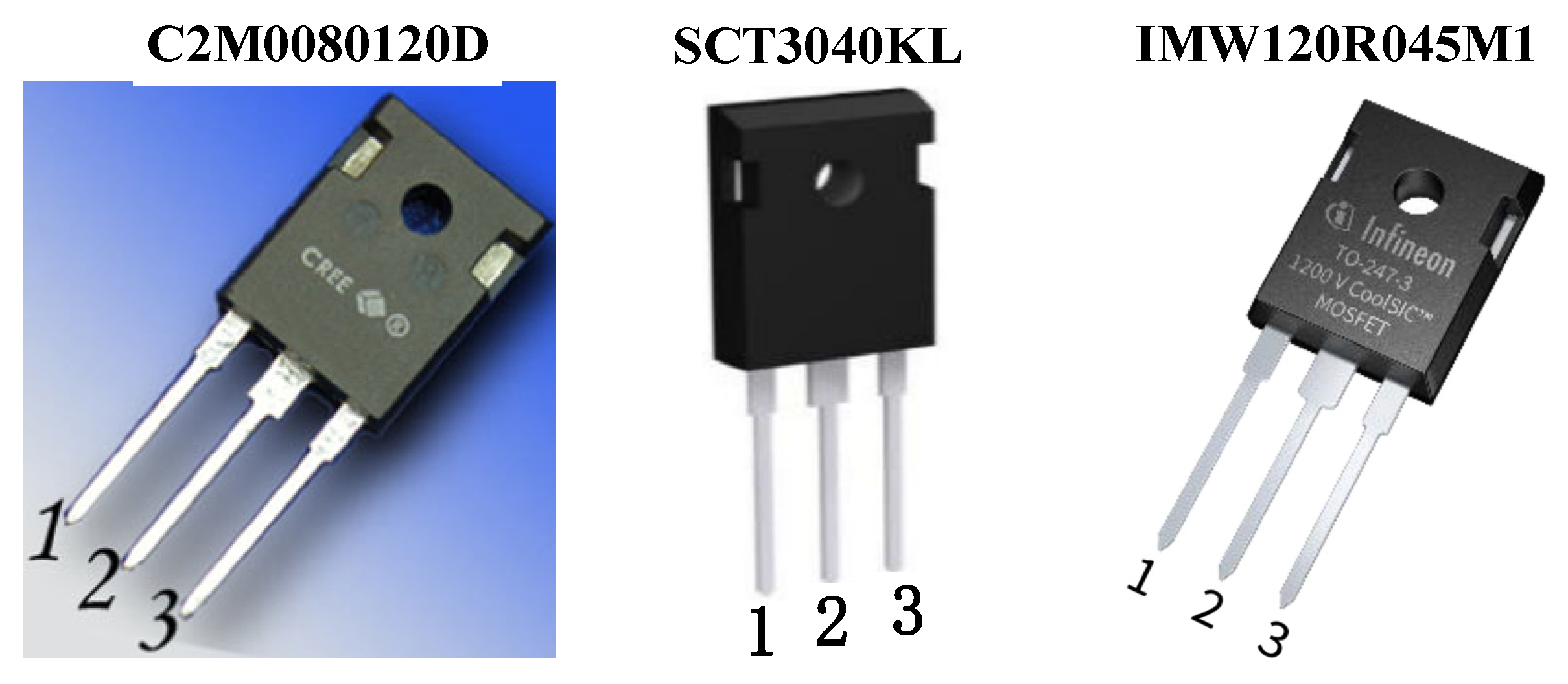
The SiC MOSFETs used in this study include the planar gate structure [35], dual trench structure [36,37] and asymmetric trench structure [38,39,40,41,42,43] (Figure 1). The SiC MOSFET with a planar gate structure (Figure 1a) has the gate electrode placed on top of the gate insulator, which is typically made of silicon dioxide (SiO2) or a high-k dielectric. The gate insulator separates the gate electrode from the channel region, controlling the flow of current. This structure allows for simple fabrication and provides good control over the channel conductivity. The SiC MOSFET with a dual trench gate structure (Figure 1b) features a trench etched into the SiC substrate, with the gate electrode positioned inside the trench. The gate insulator is formed on the trench sidewalls, isolating the gate electrode from the channel region. This structure increases the gate channel capacitance and reduces the on-resistance of the device. It also provides better control over the electric field distribution, improving the overall performance of the MOSFET. The SiC MOSFET with an asymmetric trench gate structure (Figure 1c) has a trench etched deeper on one side than on the other, creating an asymmetric electric field distribution and allowing for better control over the device characteristics. The gate insulator is formed on the trench sidewalls, as in the symmetric trench gate structure. The asymmetric trench gate structure can provide improved performance in terms of on-resistance, breakdown voltage, and switching speed. Overall, the planar gate structure is simpler to fabricate and offers good control over the channel conductivity. The symmetric and asymmetric trench gate structures provide enhanced performance in terms of on-resistance, breakdown voltage, and switching speed, but they require more complex fabrication processes. For this research, the SiC MOSFET devices used are the C2M0080120D (planar gate structure) from Cree, SCT3040KL (dual trench gate structure) from Rohm, and IMW120R045M1 (asymmetric trench gate structure) from Infineon. Their rated current/voltage values are 31.6A/1200 V, 55A/1200 V, and 52A/1200 V, respectively. All three devices employ the TO-247 package (Figure 2). The test settings are provided in Table 1. These details outline the configuration used for testing in this study.
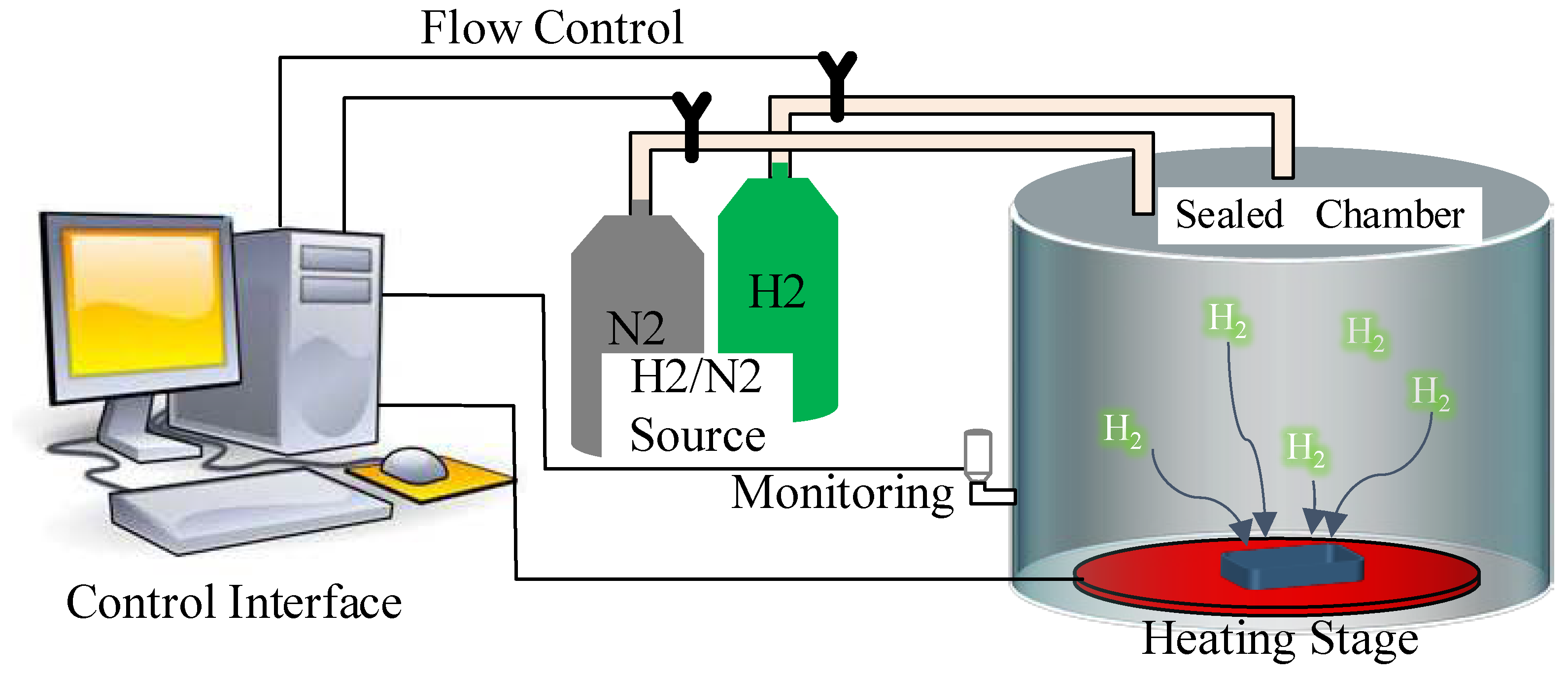
Regarding the hydrogen test setup, in this study, a self-developed atmosphere simulation test system was used to conduct hydrogen effect experiments on the three types of SiC MOSFETs, as shown in Figure 3. The atmosphere simulation test system mainly consists of a gas source, control interface, sealed chamber to conduct the hydrogen effect experiments, component monitor, and heating stage. By inputting the type and concentration ratio of the required gas in the control interface, the corresponding atmosphere can be obtained in the sealed chamber. Considering the flammable and explosive nature of hydrogen, safety precautions were taken by setting the hydrogen content at 4%, with the remaining 96% consisting of nitrogen. During the experiment, the three types of SiC MOSFETs were first placed in the above-mentioned gas environment at room temperature for 500 h, allowing sufficient time for hydrogen to enter the device. Subsequently, the MOSFETs were subjected to the same gas environment at 100 °C for either 200 h or 500 h, which was to observe if the high temperature would accelerate the change in device performance. Following this, the devices were returned to room temperature and kept for an additional 1250 h to determine if the device performance would recover. Finally, the devices were placed at 200 °C for 500 h. Before and after each experiment, the device characteristics of the three types of SiC MOSFETs were characterized using the semiconductor parameter analysis systems (Keysight B1505 and Keysight B1500) to observe the changes in device electrical performance. All the terminals of the SiC power MOSFETs were floating during the hydrogen effect experiments. And due to the strong penetration of hydrogen gas, the devices were not unpacked during the hydrogen effect experiments.
Regarding the high accelerated temperature and humidity stress test (HAST) setup, in this study, the HAST method was employed to investigate the influence of high temperature, high humidity environments on the three types of SiC MOSFETs. HAST tests can increase the pressure of water vapor within the container, which can enable temperatures to exceed 100 °C and accelerate the aging effect of water vapor penetration into the components. An EHS-211MD HAST chamber was used to perform the HAST tests on the three types of SiC MOSFETs. In order to observe the direct impact of the temperature and humidity environmental stress on the SiC MOSFETs and to avoid degradation failure caused by voltage bias, the unbiased HAST (UHAST) test was conducted. Unlike traditional HAST tests, which involve applying voltage bias, the UHAST test eliminates voltage bias to focus solely on the effects of temperature and humidity. The temperature stress, humidity stress, and pressure applied in the chamber during the experiment were set to 130 °C, 85% RH, and 230 kPa. Before and after the HAST test, the characteristics of the three different structures of SiC MOSFETs were primarily characterized every 100 h to observe any changes in device electrical performance. And during the UHAST test, the devices were unpacked.

3. Results and Discussion

3.1. The Influence of Hydrogen Gas on SiC MOSFETs

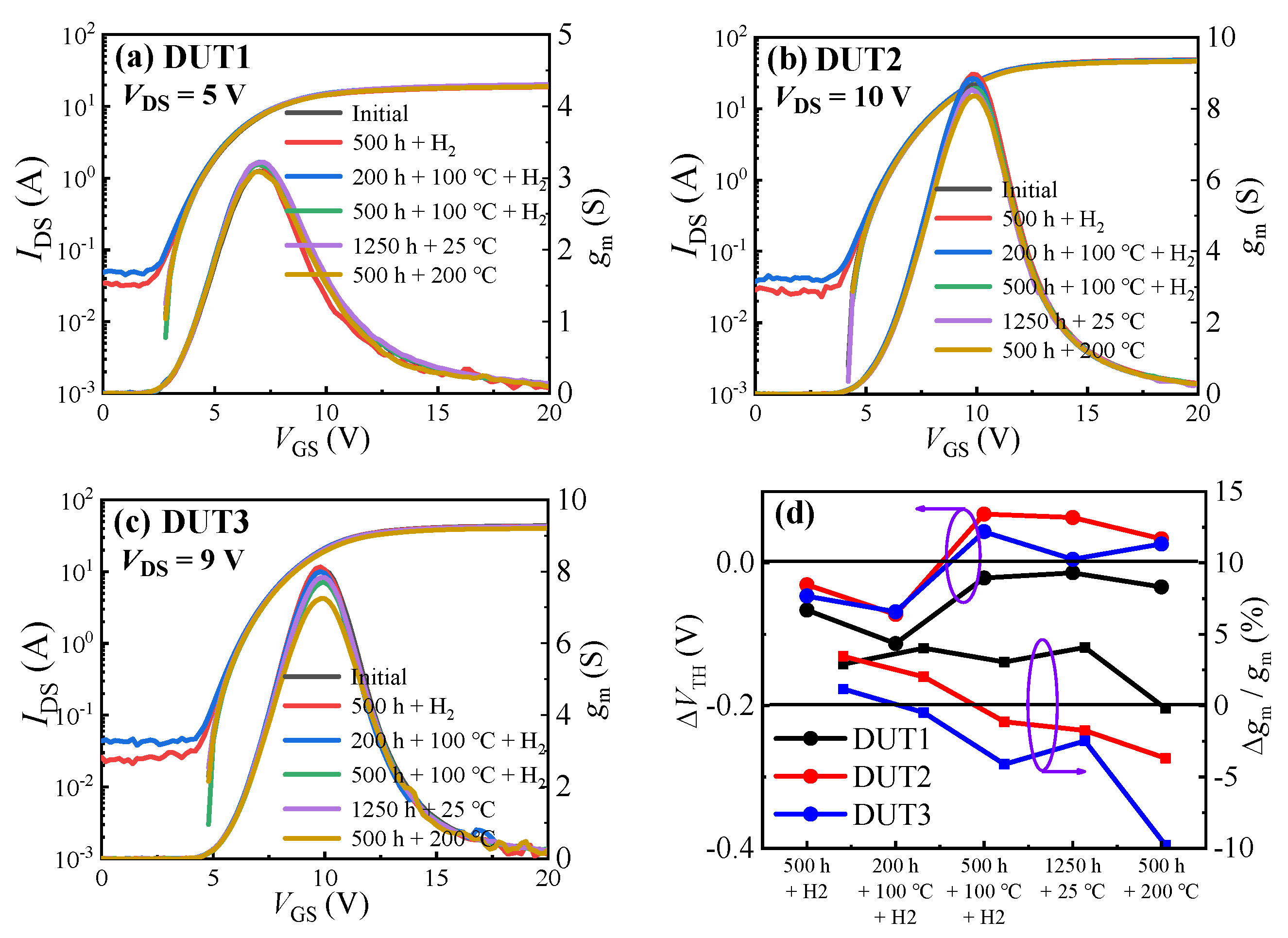
Figure 4 depicts the transfer characteristic curves before and after the hydrogen effect experiments for the three types of SiC MOSFETs. It can be observed that, after 500 h in a hydrogen environment, the planar gate structure SiC MOSFET showed a 2.89% increase in maximum transconductance (gm_max) and a 0.07 V negative drift in threshold voltage. The dual gate groove structure SiC MOSFET exhibited a 3.34% increase in gm_max and a 0.03 V negative drift in threshold voltage. The asymmetric groove structure SiC MOSFET demonstrated a 1.16% increase in gm_max and a 0.05 V negative drift in threshold voltage. This implies that all three types of SiC MOSFETs experienced an increase in gm_max and a negative drift in threshold voltage after 500 h in a hydrogen environment. Notably, the planar gate structure SiC MOSFET exhibited the largest negative drift in threshold voltage, while the dual gate groove structure SiC MOSFET demonstrated the largest change in gm_max. As mentioned in [18,19,20,21,44], hydrogen molecules can dissociate into hydrogen atoms under Au catalysis. Then, the hydrogen atoms can lose an electron due to the attraction of the Si nucleus, eventually forming H+ ions. The H+ ions can increase the positive fixed charges in the oxide of SiC MOSFETs, leading to a negative drift in threshold voltage. Additionally, hydrogen atoms can increase the electron mobility in the gate channel of SiC MOSFETs, thereby increasing the devices’ transconductance [18,19,20,21]. According to the following Formula (1) [45], the maximum transconductance of the device is mainly related to the carrier mobility. Therefore, the change in gm_max can reflect the change in carrier mobility.
g m _ max = 1.3 W g L g C ox μ V D S
where Wg and Lg are the gate width and gate length, respectively, Cox is the gate oxide layer capacitance, and VDS is the drain voltage. After maximum transconductance, the main reason for the decrease in the transconductance of the device is that the carrier concentration increases with the increase in gate voltage, and the enhanced collision scattering between carriers leads to a decrease in carrier mobility, resulting in a decrease in transconductance.
After the three types of SiC MOSFETs were subjected to a hydrogen environment at 100 °C for 200 h, the devices’ threshold voltage continued to drift negatively, but, except for the planar gate structure SiC MOSFET, the maximum transconductance of the other two structures of SiC MOSFETs started to decrease. The threshold voltage of the three structures of SiC MOSFETs drifted negatively by 0.05 V, 0.04 V, and 0.02 V, respectively. The maximum transconductance of the planar gate structure SiC MOSFET increased by 1.13%, while the maximum transconductance of the other two structures of SiC MOSFETs decreased by 1.43% and 1.66%, respectively. Subsequently, when the three types of SiC MOSFETs were subjected to a 100 °C hydrogen environment for an additional 300 h, notable changes occurred. All the devices exhibited positive drifts in threshold voltage, with values of 0.09 V, 0.14 V, and 0.11 V for the three structures, respectively. Furthermore, the maximum transconductance of all three structures decreased by 0.96%, 3.15%, and 3.61%, respectively. In other words, high temperature does not accelerate the impact of hydrogen on SiC MOSFETs; instead, it leads to device performance degradation. In addition, prolonged exposure to high temperatures may increase the stress on the devices’ SiO2/SiC interface, leading to a decrease in electron mobility and subsequently reducing the device transconductance.
To validate this hypothesis, we first placed three types of SiC MOSFETs at room temperature for 1250 h, and then placed them in a 200 °C environment for 500 h to observe the changes in device performance. After being placed at room temperature for 1250 h, the performance of the devices remained largely unchanged. However, after being placed in a 200 °C environment for 500 h, there was no significant change in the threshold voltage of the devices, but their maximum transconductance showed a significant decrease. The maximum transconductance of the three structures of SiC MOSFETs decreased by 4.28%, 1.93%, and 7.30%, respectively. This indicates that high temperature does not increase or decrease the positive fixed charges in the oxide of SiC MOSFETs, and thus does not alter the devices’ threshold voltage. However, prolonged thermal stress increases the stress on the SiO2/SiC interface [46], leading to a decrease in electron mobility at the channel and further reducing the devices’ transconductance.
Figure 5 illustrates the output characteristic curves of the three types of SiC MOSFETs before and after the experiment. Firstly, after subjecting the devices to 500 h in a hydrogen environment, the conduction currents (@ VGS/VDS = 13 V/3 V) of the three types of SiC MOSFETs increased by 2.001%, 1.73%, and 1.75% respectively. The increase in the conduction current of the devices is mainly attributed to the decrease in device threshold voltage and the increase in transconductance. And after 200 h in a 100 °C hydrogen environment, the conduction currents of the devices remained largely unchanged. However, further increasing the storage time in a 100 °C hydrogen environment will result in a significant decrease in the conduction current of the devices. After 500 h in a 100 °C hydrogen environment, the three types of SiC MOSFETs decreased by 0.50%, 3.16%, and 4.35%, respectively. This is due to the increase in device threshold voltage and the decrease in transconductance. As mentioned above, the prolonged exposure to high temperatures may increase the stress on the gate oxide interface of the chip, subsequently leading to a decrease in electron mobility at the channel and reducing the device transconductance. Additionally, after being placed at room temperature for 1250 h, the devices exhibited relatively unchanged performance. However, upon exposure to a 200 °C environment for 500 h, a significant decrease in conduction current was observed. Specifically, the conduction currents of the three SiC MOSFET structures decreased by 2.36%, 1.86%, and 5.10%, respectively. The conduction current fluctuation of asymmetric gate SiC MOSFET was larger than that of planar gate SiC MOSFET. This may result from the fact that the current fabrication process for the planar gate SiC MOSFET is more mature than that for the asymmetric gate SiC MOSFET, resulting in a relatively smaller potential reliability problem for the planar gate SiC MOSFET. On the other hand, the asymmetric gate SiC MOSFET may face greater reliability challenges. Consequently, the performance of the asymmetric gate SiC MOSFET may experience more noticeable variations when exposed to external environmental factors.
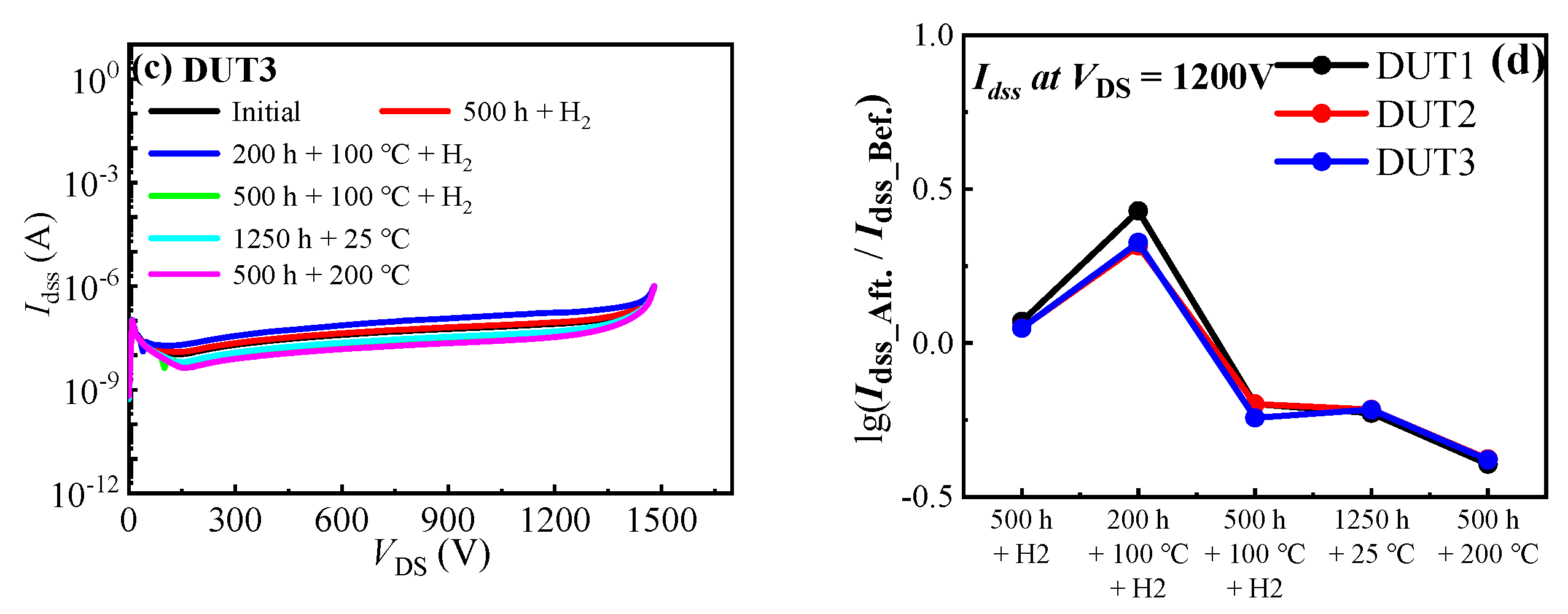
Figure 6 depicts the drain leakage current characteristics curves of the three types of SiC MOSFETs before and after the hydrogen effect experiments. Firstly, after subjecting the devices to 500 h in a hydrogen environment, the drain leakage current of all the SiC MOSFETs slightly increased. It is possible that the increase in the devices’ drain leakage current is due to the penetration of hydrogen atoms into the silicon carbide material and their interaction with impurities or defects present in the silicon carbide material. This may lead to the formation of or increase in leakage paths, resulting in an increase in the leakage current of the devices. And after 200 h in a 100 °C hydrogen environment, the drain leakage currents of the three types of SiC MOSFETs continued to increase. However, further increasing the storage time in a 100 °C hydrogen environment will result in a significant decrease in the leakage current of the devices, which may result from the fact that the high temperatures can repair some lattice damage and reduce the defect density in the silicon carbide material, thereby reducing leakage pathways and further decreasing leakage current. This can be validated by observing a significant decrease in leakage current of the device after it is subjected to a high temperature environment of 200 °C for 500 h.

3.2. The Influence of High Temperature, High Humidity Environments on SiC MOSFETs

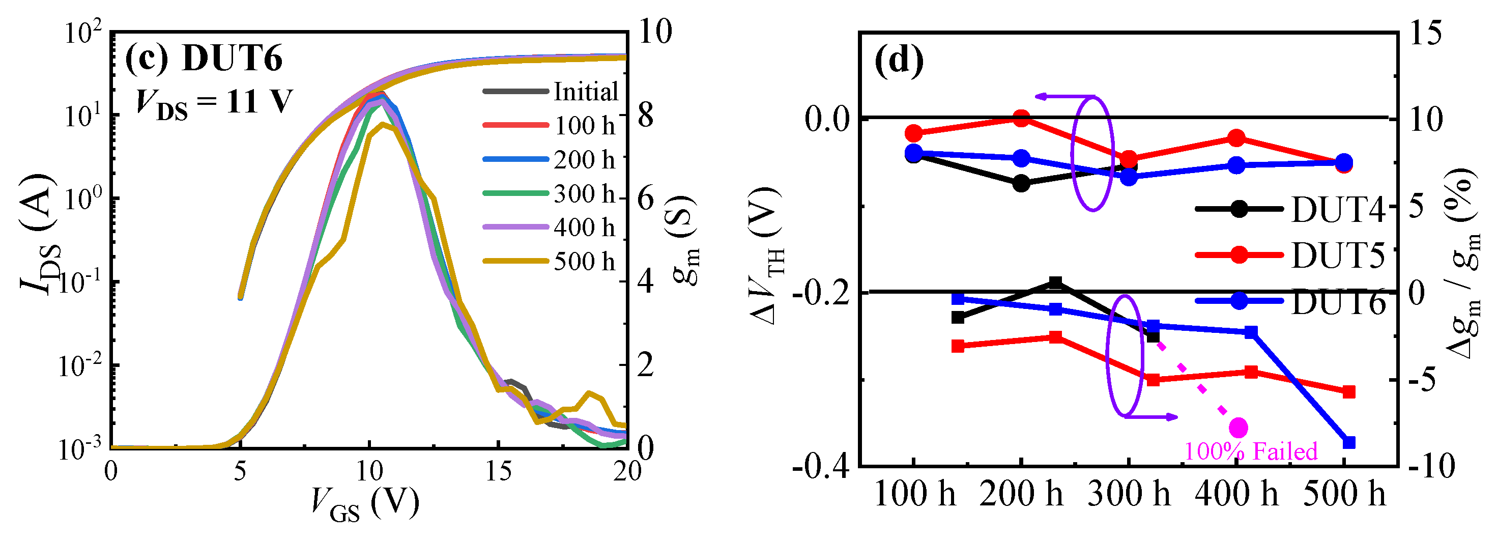
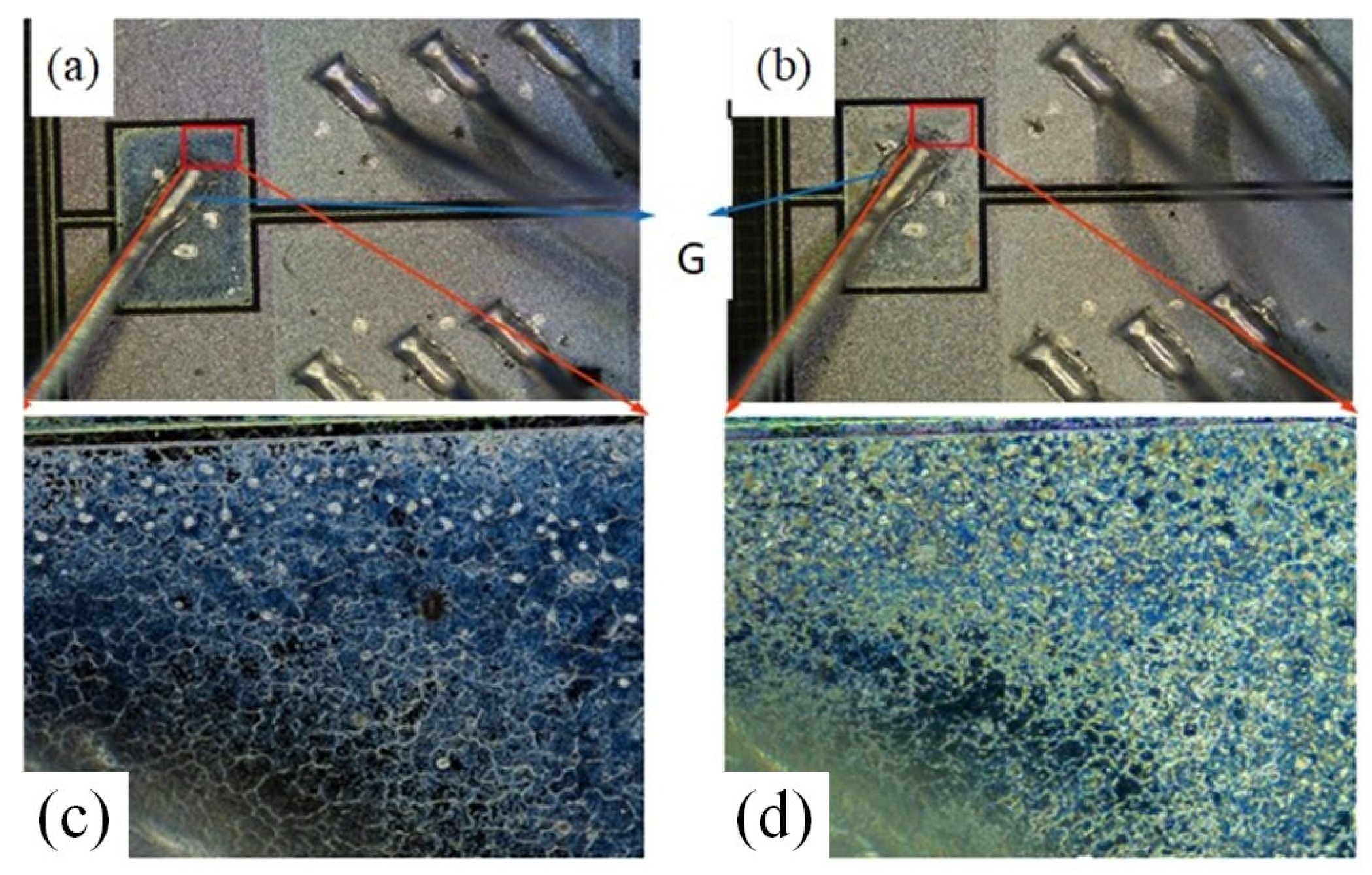
Figure 7 displays the transfer characteristics curves of the three types of SiC MOSFETs before and after the UHAST experiments. After subjecting the devices to 400 h of UHAST experiments, the planar gate structure SiC MOSFET failed. Before the failure occurred, the threshold voltage of the device experienced a certain amount of negative drift. No obvious pattern was observed in the variation in the devices’ maximum transconductance. Both the dual gate groove structure and asymmetric groove structure SiC MOSFETs also exhibited a slight negative drift in device threshold voltage and a slight decrease in device maximum transconductance after 500 h of UHAST experiments. The drift amount of threshold voltage did not increase with the duration of the UHAST experiment, but the devices’ maximum transconductances gradually decreased with the duration of the experiment. This may because the presence of moisture in UHAST experiments can lead to corrosion of the devices’ metal contacts and interconnects, which can increase the devices’ resistance and lead to the decrease in the devices’ maximum transconductance. The failure of the planar gate structure SiC MOSFET after 400 h of UHAST experiments could be due to a break in the drain or source electrode of the device. Figure 8 gives the optical images of the C2M0080120D before and after UHAST. The gate metal of SiC MOSFETs is generally copper or aluminum, which are more susceptible to oxidation and corrosion, subsequently causing a disconnection between the gate metal and the bonding wire. The gate metal turned green, possibly due to the oxidation of the copper on the surface of the gate metal. There was a significant difference in the surface color of the gate metal area of the device, which may indicate that the gate metal on the device surface had been oxidized and corroded.
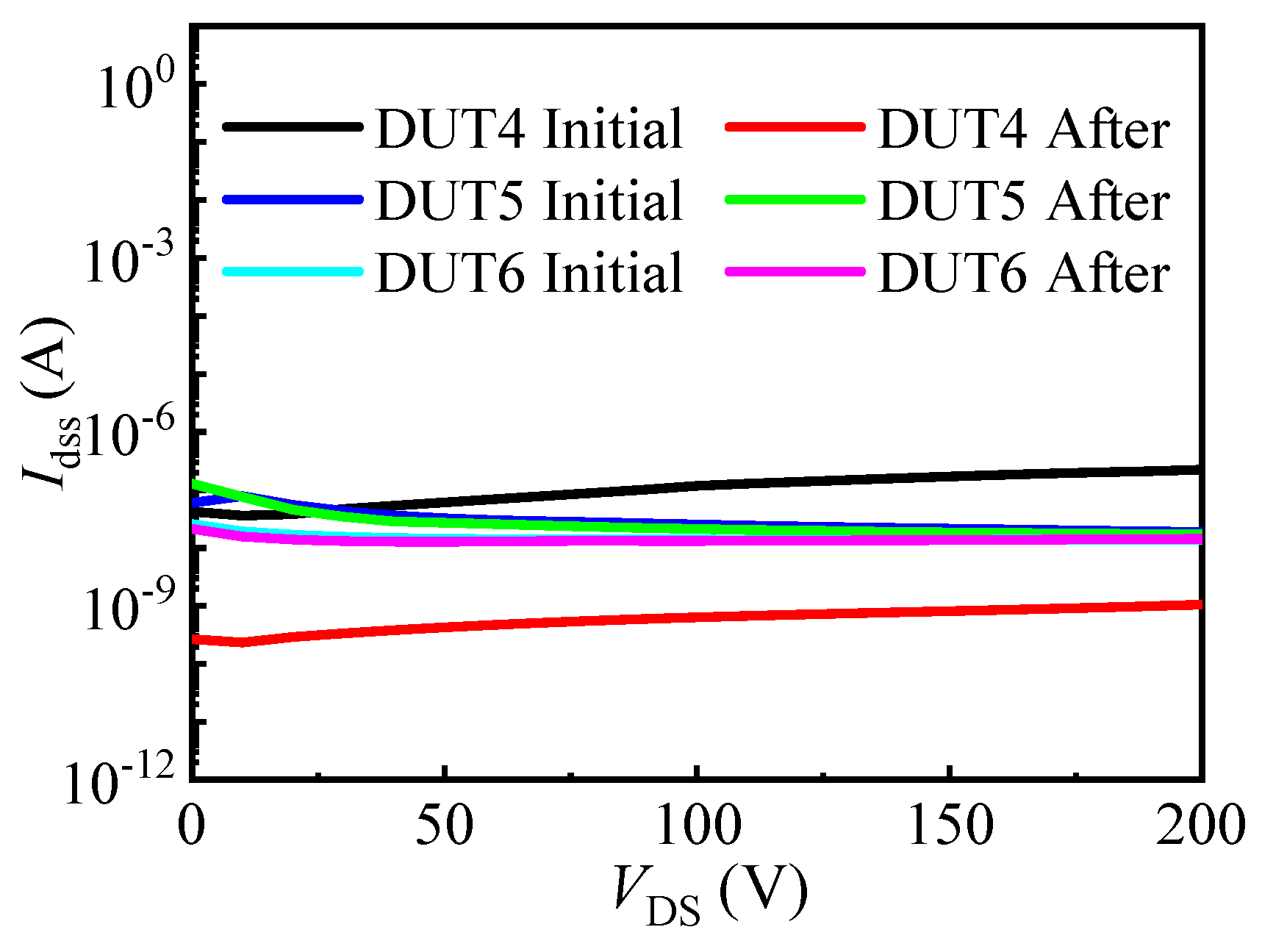
Figure 9 presents the output characteristic curves of the three types of SiC MOSFETs before and after the UHAST experiments. It can be observed that the conduction currents (@ VGS/VDS = 18 V (20 V)/3 V) of all the SiC MOSFETs gradually decreased with the duration of the experiment. Before failure occurred in the planar gate structure SiC MOSFET, its conduction currents decreased by 3.17%. And after 500 h of UHAST experiments, the conduction currents of the other two structures of SiC MOSFETs decreased by 5.20% and 2.90%, respectively. As mentioned above, the presence of moisture in the UHAST experiment can lead to corrosion of the devices’ metal contacts and interconnects, which can increase the devices’ resistance, leading to the decrease in the devices’ conduction currents. Figure 10 displays the drain leakage current characteristics curves of the three types of SiC MOSFETs before and after the UHAST experiments. It can be observed that, after failure occurred in the planar gate structure SiC MOSFET, its drain leakage current decreased by more than two orders of magnitude. This further supports the possibility of a breakage in the drain or source electrode of the planar gate structure SiC MOSFET after 400 h of UHAST experiments. For the dual trench structure and asymmetric trench structure SiC MOSFETs, their drain leakage current remained largely unchanged after 500 h of UHAST experiments.

4. Conclusions

This work investigates the influences of hydrogen gas and high temperature, high humidity environments on the performance of SiC MOSFETs. The SiC MOSFETs exhibited a negative drift in threshold voltage, an increase in maximum transconductance, and an increase in drain current after the hydrogen effect experiment. And through long-term high temperature hydrogen effect experiments, it is found that high temperature does not accelerate the impact of hydrogen on the devices and electron mobility; instead, the prolonged exposure to high temperatures may increase the stress on the SiO2/SiC interface, leading to a decrease in electron mobility, subsequently reducing the transconductance and drain current. In the high temperature, high humidity experiment, it is found that high temperature, high humidity environments can cause a certain negative drift in the devices’ threshold voltage. Furthermore, the maximum transconductance and drain current gradually decreased as the duration of the experiments increased, which may because the presence of moisture can lead to corrosion of the devices’ metal contacts and interconnects.

Author Contributions

Conceptualization, Z.H., Y.S., S.H., Z.L. and Y.H.; methodology, Z.H., J.J., Y.H. and S.H.; validation, Z.H., Y.S., S.H. and J.J.; formal analysis, Z.H., Y.S., S.H. and J.J.; investigation, Y.S., S.H. and J.J.; data curation, Y.S., S.H., Z.Z. and J.J.; writing—original draft preparation, Y.S., Z.L. and Y.H.; writing—review and editing, Y.S., Z.L., Y.C. and Y.H.; visualization, Y.S., Z.L., G.L. and Y.H.; supervision, G.L., Z.Z., Z.L. and Y.H.; project administration, Y.S.; funding acquisition, Y.S., Y.C. and Z.H. All authors have read and agreed to the published version of the manuscript.

Funding

This research was supported by the National Natural Science Foundation of China (NSFC) under Grant Nos. 52107184, 62004046 and 62274043, the National Key R&D Program of China under grant No. 2021YFB3602300, the Natural Science Foundation of Guangdong Province under Grant No. 2022A1515012127 and the Guangzhou Basic and Applied Basic Research Project under Grant No. 202201010868.

Institutional Review Board Statement

Not applicable.

Data Availability Statement

Data are available on request.

Conflicts of Interest

The authors declare no conflict of interest.

References

  1. Wang, H.; Wang, F.; Zhang, J. Power Semiconductor Device Figure of Merit for High-Power-Density Converter Design Applications. IEEE Trans. Electron Devices 2008, 55, 466–470. [Google Scholar] [CrossRef]
  2. Shen, Z.J.; Omura, I. Power Semiconductor Devices for Hybrid, Electric, and Fuel Cell Vehicles. Proc. IEEE 2007, 95, 778–789. [Google Scholar] [CrossRef]
  3. Zhang, L.; Zheng, Z.; Lou, X. A review of WBG and Si devices hybrid applications. Chin. J. Electr. Eng. 2021, 7, 1–20. [Google Scholar] [CrossRef]
  4. Ding, X.; Zhou, Y.; Cheng, J. A review of gallium nitride power device and its applications in motor drive. CES Trans. Electr. Mach. Syst. 2019, 3, 54–64. [Google Scholar] [CrossRef]
  5. Rafin, S.M.S.H.; Ahmed, R.; Mohammed, O.A. Wide Band Gap Semiconductor Devices for Power Electronic Converters. In Proceedings of the 2023 Fourth International Symposium on 3D Power Electronics Integration and Manufacturing (3D-PEIM), Miami, FL, USA, 1–3 February 2023; pp. 1–8. [Google Scholar] [CrossRef]
  6. Aghdam, M.G.H.; Thiringer, T. Comparison of SiC and Si power semiconductor devices to be used in 2.5 kW DC/DC converter. In Proceedings of the 2009 International Conference on Power Electronics and Drive Systems (PEDS), Taipei, Taiwan, 2–5 November 2009; pp. 1035–1040. [Google Scholar] [CrossRef]
  7. Hamada, K.; Nagao, M.; Ajioka, M.; Kawai, F. SiC—Emerging Power Device Technology for Next-Generation Electrically Powered Environmentally Friendly Vehicles. IEEE Trans. Electron Devices 2015, 62, 278–285. [Google Scholar] [CrossRef]
  8. Kneifel, M.; Silber, D.; Held, R. Predictive modeling of SiC-device power Schottky diode for investigations in power electronics. In Proceedings of the Applied Power Electronics Conference. APEC ‘96, San Jose, CA, USA, 3–7 March 1996; Volume 1, pp. 239–245. [Google Scholar] [CrossRef]
  9. Race, S.; Kumar, P.; Natzke, P.; Kovacevic-Badstuebner, I.; Bathen, M.E.; Grossner, U.; Romano, G.; Arango, Y.; Bolat, S.; Wirths, S.; et al. Gate Impedance Analysis of SiC power MOSFETs with SiO2 and High-k Dielectric. In Proceedings of the 2023 35th International Symposium on Power Semiconductor Devices and ICs (ISPSD), Hong Kong, China, 28 May 2023; pp. 9–12. [Google Scholar] [CrossRef]
  10. Wang, X.; Wen, H.; Zhu, Y. Review of SiC Power Devices for Electrical Power Systems: Characteristics, Protection, and Application. In Proceedings of the 2021 6th Asia Conference on Power and Electrical Engineering (ACPEE), Chongqing, China, 8–11 April 2021; pp. 1–5. [Google Scholar] [CrossRef]
  11. Su, Y.; Tu, B.; Tang, R.; Long, X. Thermal effects on fracture behaviors of the die-attachment in the SiC power device under power cyclic conditions based on fracture phase-field modeling. In Proceedings of the 2022 23rd International Conference on Electronic Packaging Technology (ICEPT), Dalian, China, 10–13 August 2022; pp. 1–4. [Google Scholar] [CrossRef]
  12. Race, S.; Ziemann, T.; Tiwari, S.; Kovacevic-Badstuebner, I.; Grossner, U. Accuracy of Thermal Analysis for SiC Power Devices. In Proceedings of the 2021 IEEE International Reliability Physics Symposium (IRPS), Monterey, CA, USA, 21–25 March 2021; pp. 1–5. [Google Scholar] [CrossRef]
  13. Mu, W.; Wang, B.; Wang, S.; Jin, H.; Li, H.; Wang, L. Comparative Study of Thermal Performance of a SiC MOSFET Power Module Integrated with Vapor Chamber for Traction Inverter Applications. In Proceedings of the 2021 IEEE Workshop on Wide Bandgap Power Devices and Applications in Asia (WiPDA Asia), Wuhan, China, 25–27 August 2021; pp. 285–289. [Google Scholar] [CrossRef]
  14. Hoffmann, F.; Kaminski, N. Impact of Device Design on the Power Cycling Capability of Discrete SiC MOSFETs at Different Temperature Swings. In Proceedings of the 2020 32nd International Symposium on Power Semiconductor Devices and ICs (ISPSD), Vienna, Austria, 17–21 May 2020; pp. 533–536. [Google Scholar] [CrossRef]
  15. Yasui, K.; Hayakawa, S.; Nakamura, M.; Kawase, D.; Ishigaki, T.; Sasaki, K.; Tabata, T.; Morita, T.; Sagawa, M.; Matsushima, H.; et al. Improvement of power cycling reliability of 3.3 kV full-SiC power modules with sintered copper technology for Tj, max = 175 °C. In Proceedings of the 2018 IEEE 30th International Symposium on Power Semiconductor Devices and ICs (ISPSD), Chicago, IL, USA, 13–17 May 2018; pp. 455–458. [Google Scholar] [CrossRef]
  16. Fayyaz, A.; Castellazzi, A. Performance and robustness testing of SiC power devices. In Proceedings of the 6th IET International Conference on Power Electronics, Machines and Drives (PEMD 2012), Bristol, UK, 27–29 March 2012; pp. 1–5. [Google Scholar] [CrossRef]
  17. Hoffmann, F.; Kaminski, N. Power Cycling Performance and Lifetime Estimation of 1700V SiC MPS Diode Modules with Multiple Chips Connected in Parallel. In Proceedings of the 2020 32nd International Symposium on Power Semiconductor Devices and ICs (ISPSD), Vienna, Austria, 17–21 May 2020; pp. 537–540. [Google Scholar] [CrossRef]
  18. Von Kamienski, B.S.; Golz, A.; Kurz, H. Defect Reduction by Post-Oxidation Annealing of Oxides on P- and N-Type 6H-SiC. In Proceedings of the ESSDERC ‘94: 24th European Solid State Device Research Conference, Edinburgh, UK, 11–15 September 1994; pp. 757–760. [Google Scholar]
  19. Ueno, K.; Asai, R.; Tsuji, T. 4H-SiC MOSFETs utilizing the H2 surface cleaning technique. IEEE Electron Device Lett. 1998, 19, 244–246. [Google Scholar] [CrossRef]
  20. Senzaki, J.; Kojima, K.; Harada, S.; Kosugi, R.; Suzuki, S.; Suzuki, T.; Fukuda, K. Excellent effects of hydrogen postoxidation annealing on inversion channel mobility of 4H-SiC MOSFET fabricated on (1120) face. IEEE Electron Device Lett. 2002, 23, 13–15. [Google Scholar] [CrossRef]
  21. Chen, Y.Q.; Zhang, Y.C.; Liu, Y.; Liao, X.Y.; En, Y.F.; Fang, W.X.; Huang, Y. Effect of Hydrogen on Defects of AlGaN/GaN HEMTs Characterized by Low-Frequency Noise. IEEE Trans. Electron Devices 2018, 65, 1321–1326. [Google Scholar] [CrossRef]
  22. Philofsky, E.; Ostrander, C.; Hartman, S. The evolution of hydrogen from plastic molding compound and its effect on the yield and reliability of ferroelectric memories. In Proceedings of the 1998 IEEE International Reliability Physics Symposium Proceedings. 36th Annual (Cat. No. 98CH36173), Reno, NV, USA, 31 March–2 April 1998; pp. 232–237. [Google Scholar] [CrossRef]
  23. Zhao, P.; Zha, Z.; Xiao, Q.; Chen, J.; Zhu, J.; Fu, Z.; Chen, Y. Degradation Behavior and Mechanism of E-mode Cascode GaN HEMTs under Hydrogen Environment. In Proceedings of the 2023 International Conference on Power Energy Systems and Applications (ICoPESA), Nanjing, China, 24–26 February 2023; pp. 728–732. [Google Scholar] [CrossRef]
  24. Ofrim, B.; Udrea, F.; Brezeanu, G.; Hsieh, A.P.-S. Hydrogen sensor based on silicon carbide (SiC) MOS capacitor. In Proceedings of the CAS 2012 (International Semiconductor Conference), Sinaia, Romania, 15–17 October 2012; pp. 367–370. [Google Scholar] [CrossRef]
  25. Shafiei, M.; Wlodarski, W.; Kalantar-Zadeh, K.; Comini, E.; Bianchi, S.; Sberveglieri, G. Pt/SnO2 Nanowires/SiC Based Hydrogen Gas Sensor. In Proceedings of the SENSORS, 2007 IEEE, Atlanta, GA, USA, 28–31 October 2007; pp. 166–169. [Google Scholar] [CrossRef]
  26. Pristavu, G.; Draghici, F.; Badila, M.; Brezeanu, G.; Pascu, R.; Craciunoiu, F. High temperature SiC-sensors. In Proceedings of the 2014 IEEE 20th International Symposium for Design and Technology in Electronic Packaging (SIITME), Bucharest, Romania, 23–26 October 2014; pp. 329–332. [Google Scholar] [CrossRef]
  27. Wang, Y.; Deng, E.; Wu, L.; Yan, Y.; Zhao, Y.; Huang, Y. Influence of Humidity on the Power Cycling Lifetime of SiC MOSFETs. IEEE Trans. Components Packag. Manuf. Technol. 2022, 12, 1781–1790. [Google Scholar] [CrossRef]
  28. Wang, Y.; Deng, E.; Wu, L.; Cao, H.; Yan, Y.; Zeng, P.; Zhang, Y.; Zhao, Y.; Huang, Y. Advanced Power Cycling Test Integrated with Voltage, Current, Temperature, and Humidity Stress. IEEE Trans. Power Electron. 2023, 38, 7685–7696. [Google Scholar] [CrossRef]
  29. Brunko, A.; Gloth, M.; Kaminski, N. Humidity Capability of Enhancement Mode GaN High Electron Mobility Transistors. In Proceedings of the 2021 IEEE 8th Workshop on Wide Bandgap Power Devices and Applications (WiPDA), Redondo Beach, CA, USA, 7–11 November 2021; pp. 242–245. [Google Scholar] [CrossRef]
  30. Ji, I.-H.; Mathew, A.; Park, J.-H.; Oldham, N.; McCain, M.; Sabri, S.; Van Brunt, E.; Hull, B.; Lichtenwalner, D.J.; Gajewski, D.A.; et al. High Temperature and High Humidity Reliability Evaluation of Large-Area 1200V and 1700V SiC Diodes. In Proceedings of the 2023 IEEE International Reliability Physics Symposium (IRPS), Monterey, CA, USA, 26–30 March 2023; pp. 1–4. [Google Scholar] [CrossRef]
  31. Kaminski, N.; Rugen, S.; Hoffmann, F. Gaining Confidence—A Review of Silicon Carbide’s Reliability Status. In Proceedings of the 2019 IEEE International Reliability Physics Symposium (IRPS), Monterey, CA, USA, 31 March–4 April 2019; pp. 1–7. [Google Scholar] [CrossRef]
  32. Kumar, V.; Verma, J.; Maan, A.; Akhtar, J. Epitaxial 4H–SiC based Schottky diode temperature sensors in ultra-low current range. Vacuum 2020, 182, 109590. [Google Scholar] [CrossRef]
  33. Verma, J.; Pant, S.; Kumar, A.; Jangir, B.K.; Dalal, J.; Ram, M. Analysis of trench termination in 4H-nSiC based power devices. Mater. Today Proc. 2021, 46, 11072–11076. [Google Scholar] [CrossRef]
  34. Kumar, V.; Maan, A.S.; Akhtar, J. Barrier height inhomogeneities induced anomaly in thermal sensitivity of Ni/4H-SiC Schottky diode temperature sensor. J. Vac. Sci. Technol. B Nanotechnol. Microelectron. Mater. Process. Meas. Phenom. 2014, 32, 041203. [Google Scholar] [CrossRef]
  35. Li, Y.; Zhou, X.; Zhao, Y.; Jia, Y.; Hu, D.; Wu, Y.; Zhang, L.; Chen, Z.; Huang, A.Q. Gate Bias Dependence of VTH Degradation in Planar and Trench SiC MOSFETs under Repetitive Short Circuit Tests. IEEE Trans. Electron Devices 2022, 69, 2521–2527. [Google Scholar] [CrossRef]
  36. Singh, Y.; Dwivedi, D. Simulation Study of Dual-Gate Trench LDMOSFET on 4H-SiC. In Proceedings of the 2015 Second International Conference on Advances in Computing and Communication Engineering, Dehradun, India, 1–2 May 2015; pp. 174–177. [Google Scholar] [CrossRef]
  37. Takayanagi, R.; Taniguchi, K.; Hoya, M.; Kanai, N.; Tsuji, T.; Hori, M.; Ikeda, Y.; Maruyama, K.; Kawamura, I. 3.3kV Power Module for Electric Distribution Equipment with SiC Trench-Gate MOSFET. In Proceedings of the 2019 International Conference on Electronics Packaging (ICEP), Niigata, Japan, 17–20 April 2019; pp. 83–87. [Google Scholar] [CrossRef]
  38. Ni, W.; Wang, X.; Xu, M.; Wang, Q.; Feng, C.; Xiao, H.; Jiang, L.; Li, W. Study of Asymmetric Cell Structure Tilt Implanted 4H-SiC Trench MOSFET. IEEE Electron Device Lett. 2019, 40, 698–701. [Google Scholar] [CrossRef]
  39. Deng, X.; Li, X.; Li, X.; Zhu, H.; Xu, X.; Wen, Y.; Sun, Y.; Chen, W.; Li, Z.; Zhang, B. Short-Circuit Capability Prediction and Failure Mode of Asymmetric and Double Trench SiC MOSFETs. IEEE Trans. Power Electron. 2020, 36, 8300–8307. [Google Scholar] [CrossRef]
  40. Adhikari, M.S.; Singh, Y. High performance multi-finger MOSFET on SOI for RF amplifiers. Indian J. Phys. 2017, 91, 1211–1217. [Google Scholar] [CrossRef]
  41. Adhikari, M.S.; Patel, R.; Tripathi, S.L.; Singh, Y. Design of SOI MOSFETs for Analog/RF Circuits. Indian J. Pure Appl. Phys. 2020, 58, 678–685. [Google Scholar]
  42. Adhikari, M.S.; Singh, Y. Implementation of Trench-based Power LDMOS and Low Voltage MOSFET on InGaAs. IETE Tech. Rev. 2018, 36, 234–242. [Google Scholar] [CrossRef]
  43. Adhikari, M.S.; Patel, R.; Verma, Y.K.; Singh, Y. Implementation of Low Voltage MOSFET and Power LDMOS on InGaAs. Silicon 2022, 14, 3905–3910. [Google Scholar] [CrossRef]
  44. Gao, R.; Liu, C.; He, Z.; Chen, Y.; Shi, Y.; Lin, X.; Zhang, X.; Wang, Z.; En, Y.; Lu, G.; et al. Towards Understanding the Interaction Between Hydrogen Poisoning and Bias Stress in AlGaN/GaN MIS-HEMTs With SiNx Gate Dielectric. IEEE Electron Device Lett. 2021, 42, 212–215. [Google Scholar] [CrossRef]
  45. Liu, Y.; Chen, H.B.; He, Y.J.; Wang, X.; Yue, L.; En, Y.F.; Liu, M.H. Radiation effects on the low frequency noise in partially depleted silicon on insulator transistors. Acta Phys. Sinica. 2015, 64, 078501. [Google Scholar]
  46. Yang, S.; Zhang, Y.; Song, Q.; Tang, X.; Zhang, Y.; Yuan, L. Impact of High-Temperature Storage Stressing (HTSS) on Degradation of High-Voltage 4H-SiC Junction Barrier Schottky Diodes. IEEE Trans. Power Electron. 2018, 33, 1874–1877. [Google Scholar] [CrossRef]
Figure 1. Schematic diagram of SiC VDMOS with (a) planar gate structure, (b) double trench structure, and (c) asymmetric trench structure.
Materials 16 06193 g001
Figure 2. Package schematic of the three types of SiC MOSFETs. Note: 1, 2, and 3 are the gate, source, and drain electrodes of the device, respectively.
Materials 16 06193 g002
Figure 3. Atmospheric environment simulation test system.
Materials 16 06193 g003
Figure 4. Transfer characteristic curves before and after the hydrogen effect experiments of (a) DUT1, (b) DUT2, and (c) DUT3. (d) Summary of the changes in the devices’ gm_max and VTH.
Materials 16 06193 g004
Figure 5. Output characteristic curves before and after the hydrogen effect experiments of (a) DUT1, (b) DUT2, and (c) DUT3. (d) Summary of the change in the devices’ IDS.
Materials 16 06193 g005
Figure 6. Leakage current characteristic curves before and after the hydrogen effect experiments of (a) DUT1, (b) DUT2, and (c) DUT3. (d) Summary of the change in the devices’ Idss.
Materials 16 06193 g006aMaterials 16 06193 g006b
Figure 7. Transfer characteristic curves before and after UHAST of (a) DUT4, (b) DUT5, and (c) DUT6. (d) Summary of the change in the devices’ gm and VTH.
Materials 16 06193 g007aMaterials 16 06193 g007b
Figure 8. The optical images of the SiC MOSFET (C2M0080120D) before (a,c) and after (b,d) UHAST. (c,d) are partially enlarged images of gate region metal.
Materials 16 06193 g008
Figure 9. Output characteristic curves before and after UHAST of (a) DUT4, (b) DUT5, and (c) DUT6. (d) Summary of the change in the devices’ IDS.
Materials 16 06193 g009
Figure 10. The drain leakage current characteristic curves before and after UHAST of the three types of SiC MOSFETs.
Materials 16 06193 g010
Table 1. Test settings for each DUT.
DUT1DUT2DUT3
C2M0080120DSCT3040KLIMW120R045M1
Hydrogen effect experiments
DUT4DUT5DUT6
C2M0080120DSCT3040KLIMW120R045M1
High Accelerated Temperature and Humidity Stress Test
Disclaimer/Publisher’s Note: The statements, opinions and data contained in all publications are solely those of the individual author(s) and contributor(s) and not of MDPI and/or the editor(s). MDPI and/or the editor(s) disclaim responsibility for any injury to people or property resulting from any ideas, methods, instructions or products referred to in the content.