

Fano Resonances in Metal Gratings with Sub-Wavelength Slits on High Refractive Index Silicon
 ,
,
Abstract
:1. Introduction
2. Analysis and Modeling
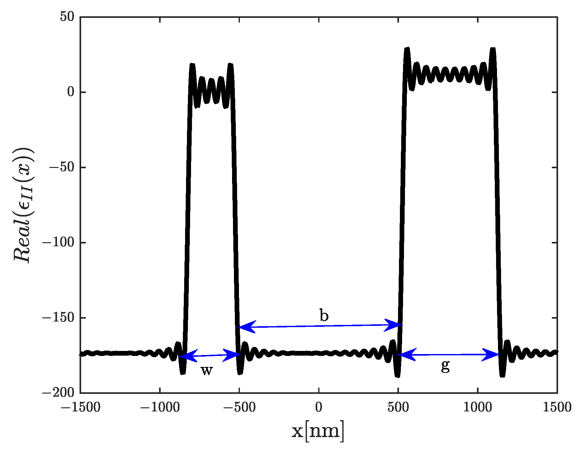
2.1. Design and Excitation Source
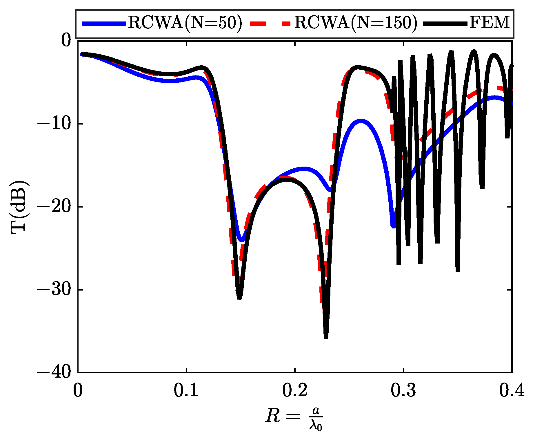
2.2. The Rigorous Coupled Wave Analysis (RCWA) Method
- The transmission spectrum in decibels, denoted as , is given by Equation (14):
3. Results and Discussion
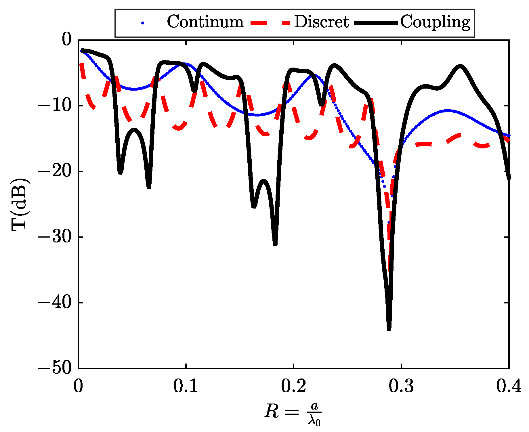
3.1. Design and Characterization of the Continuum State
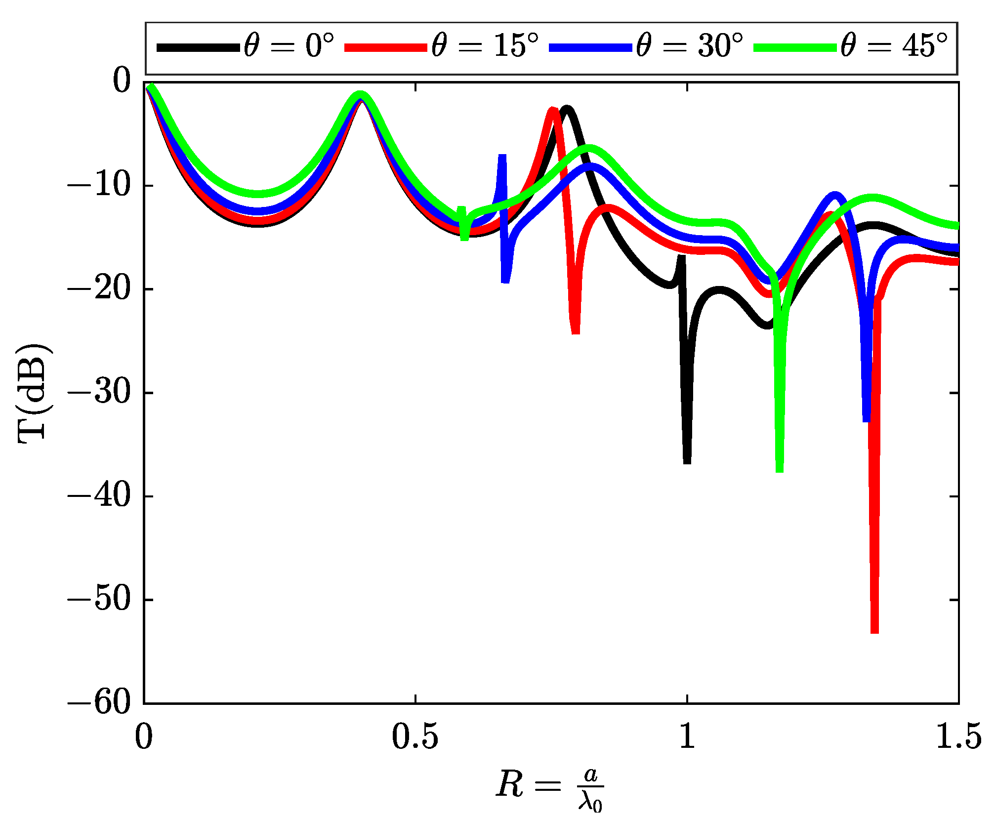
3.2. Characterization of Rayleigh Anomalies at Different Angle of Incidence
3.3. Discrete State Design
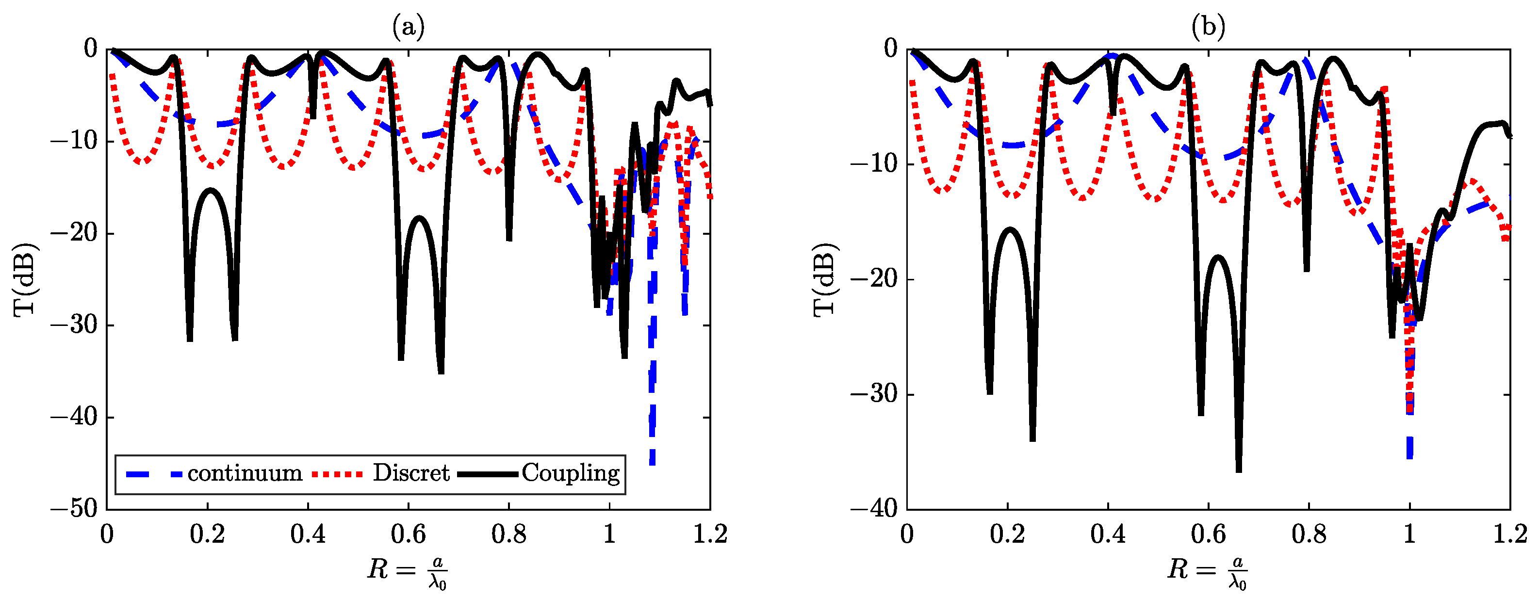
3.4. Coupling between Continuum and Discrete States
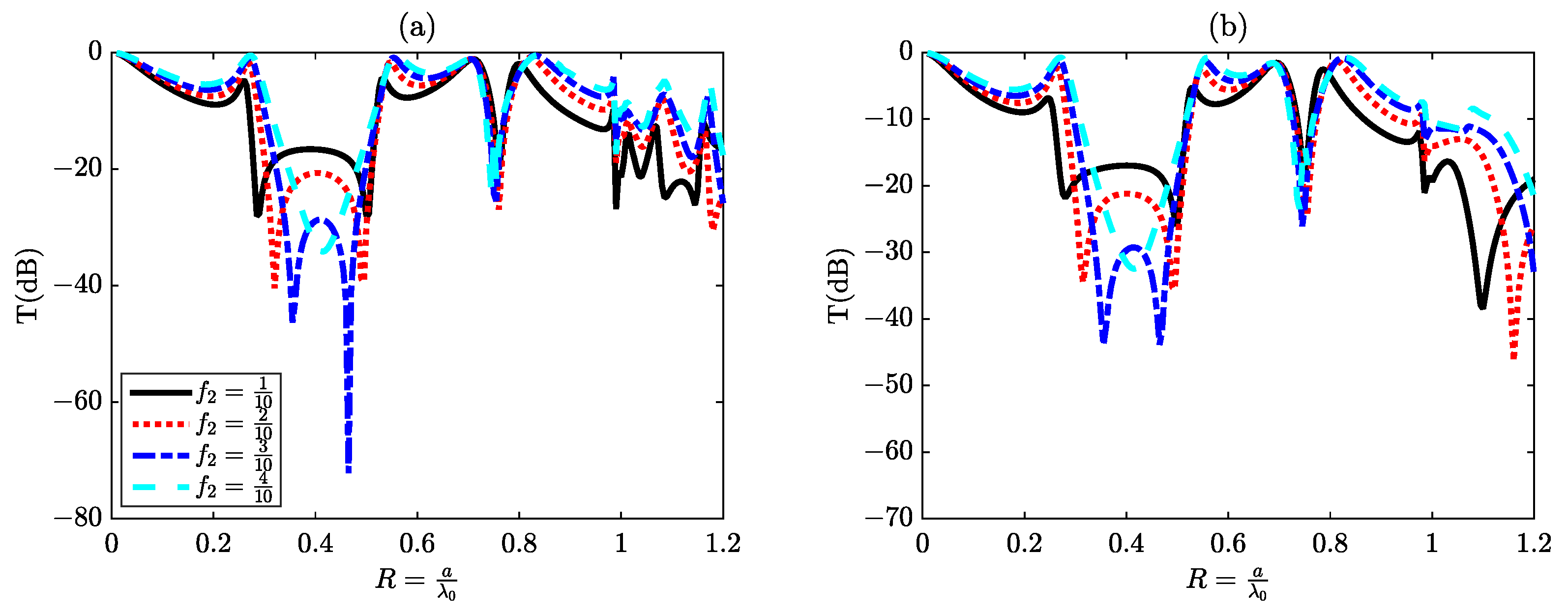
3.5. The Effect of the Filling Factor of Silicon (Si) Slits on Resonances
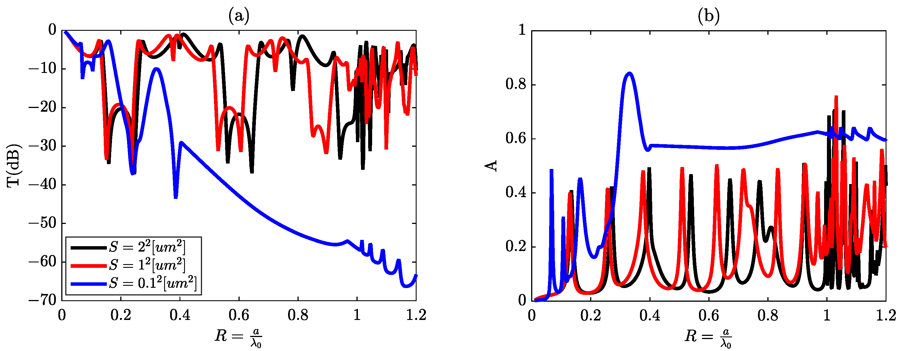
3.6. Scaling Factor
- If :
- If :
- If :
3.7. The Effect of the Substrate on the Response of the Structure
4. Conclusions
Author Contributions
Funding
Institutional Review Board Statement
Informed Consent Statement
Data Availability Statement
Conflicts of Interest
References
- Luk’Yanchuk, B.; Zheludev, N.I.; Maier, S.A.; Halas, N.J.; Nordlander, P.; Giessen, H.; Chong, C.T. The Fano resonance in plasmonic nanostructures and metamaterials. Nat. Mater. 2010, 9, 707–715. [Google Scholar] [CrossRef]
- Lv, J.; Shen, S.; Chen, L.; Zhu, Y.; Zhuang, S. Frequency selective fingerprint sensor: The Terahertz unity platform for broadband chiral enantiomers multiplexed signals and narrowband molecular AIT enhancement. PhotoniX 2023, 4, 1–14. [Google Scholar]
- Miroshnichenko, A.E.; Flach, S.; Kivshar, Y.S. Fano resonances in nanoscale structures. Rev. Mod. Phys. 2010, 82, 2257. [Google Scholar] [CrossRef]
- Lee, K.L.; Hsu, H.Y.; You, M.L.; Chang, C.C.; Pan, M.Y.; Shi, X.; Ueno, K.; Misawa, H.; Wei, P.K. Highly sensitive aluminum-based biosensors using tailorable Fano resonances in capped nanostructures. Sci. Rep. 2017, 7, 44104. [Google Scholar] [CrossRef]
- Zhao, W.; Leng, X.; Jiang, Y. Fano resonance in all-dielectric binary nanodisk array realizing optical filter with efficient linewidth tuning. Opt. Express 2015, 23, 6858–6866. [Google Scholar] [CrossRef]
- Fano, U. Sullo spettro di assorbimento dei gas nobili presso il limite dello spettro d’arco. Il Nuovo Cimento (1924–1942) 1935, 12, 154–161. [Google Scholar] [CrossRef]
- Fano, U. Effects of configuration interaction on intensities and phase shifts. Phys. Rev. 1961, 124, 1866. [Google Scholar] [CrossRef]
- Deng, Z.L.; Yogesh, N.; Chen, X.D.; Chen, W.J.; Dong, J.W.; Ouyang, Z.; Wang, G.P. Full controlling of Fano resonances in metal-slit superlattice. Sci. Rep. 2015, 5, 18461. [Google Scholar] [CrossRef]
- Ngo, Q.M.; Le, K.Q.; Vu, D.L. Optical bistability based on Fano resonances in single-and double-layer nonlinear slab waveguide gratings. JOSA B 2014, 31, 1054–1061. [Google Scholar] [CrossRef]
- Liu, D.; Yu, X.; Wu, F.; Cao, J.; Zhao, Y.; Shi, H.; Xiao, S.; Kuwahara, M.; Itoigawa, F.; Ono, S.; et al. High-quality resonances in terahertz composite slabs based on metal gratings. J. Opt. 2022, 24, 105103. [Google Scholar] [CrossRef]
- Liu, F.; Cai, F.; Ding, Y.; Liu, Z. Tunable transmission spectra of acoustic waves through double phononic crystal slabs. Appl. Phys. Lett. 2008, 92, 103504. [Google Scholar] [CrossRef]
- Genet, C.; van Exter, M.P.; Woerdman, J. Fano-type interpretation of red shifts and red tails in hole array transmission spectra. Opt. Commun. 2003, 225, 331–336. [Google Scholar] [CrossRef]
- Fan, S.; Suh, W.; Joannopoulos, J.D. Temporal coupled-mode theory for the Fano resonance in optical resonators. JOSA A 2003, 20, 569–572. [Google Scholar] [CrossRef] [PubMed]
- Bandopadhyay, S.; Dutta-Roy, B.; Mani, H. Understanding the Fano resonance through toy models. Am. J. Phys. 2004, 72, 1501–1507. [Google Scholar] [CrossRef]
- Pennec, Y.; Rouhani, B.D.; Larabi, H.; Akjouj, A.; Leveque, G. Perpendicular transmission of acoustic waves between two substrates connected by sub-wavelength pillars. New J. Phys. 2012, 14, 073039. [Google Scholar] [CrossRef]
- Estrada, H.; Candelas, P.; Uris, A.; Belmar, F.; Meseguer, F.; de Abajo, F.J.G. Sound transmission through perforated plates with subwavelength hole arrays: A rigid-solid model. Wave Motion 2011, 48, 235–242. [Google Scholar] [CrossRef]
- Christensen, J.; Martin-Moreno, L.; Garcia-Vidal, F.J. Theory of resonant acoustic transmission through subwavelength apertures. Phys. Rev. Lett. 2008, 101, 014301. [Google Scholar] [CrossRef]
- Wood, R.W. XLII. On a remarkable case of uneven distribution of light in a diffraction grating spectrum. Lond. Edinb. Dublin Philos. Mag. J. Sci. 1902, 4, 396–402. [Google Scholar] [CrossRef]
- Rayleigh, L. III. Note on the remarkable case of diffraction spectra described by Prof. Wood. Lond. Edinb. Dublin Philos. Mag. J. Sci. 1907, 14, 60–65. [Google Scholar] [CrossRef]
- Wood, R.W. XXVII. Diffraction gratings with controlled groove form and abnormal distribution of intensity. Lond. Edinb. Dublin Philos. Mag. J. Sci. 1912, 23, 310–317. [Google Scholar] [CrossRef]
- Wood, R.W. Anomalous diffraction gratings. Phys. Rev. 1935, 48, 928. [Google Scholar] [CrossRef]
- Fano, U. The theory of anomalous diffraction gratings and of quasi-stationary waves on metallic surfaces (Sommerfeld’s waves). JOSA 1941, 31, 213–222. [Google Scholar] [CrossRef]
- Hessel, A.; Oliner, A. A new theory of Wood’s anomalies on optical gratings. Appl. Opt. 1965, 4, 1275–1297. [Google Scholar] [CrossRef]
- Maystre, D.; Neviere, M. Quantitative theoretical study of the plasmon anomalies of diffraction gratings. J. Opt. 1977, 8, 165. [Google Scholar] [CrossRef]
- Porto, J.; Garcia-Vidal, F.; Pendry, J. Transmission resonances on metallic gratings with very narrow slits. Phys. Rev. Lett. 1999, 83, 2845. [Google Scholar] [CrossRef]
- Collin, S.; Pardo, F.; Teissier, R.; Pelouard, J.L. Strong discontinuities in the complex photonic band structure of transmission metallic gratings. Phys. Rev. B 2001, 63, 033107. [Google Scholar] [CrossRef]
- Ebbesen, T.W.; Lezec, H.J.; Ghaemi, H.; Thio, T.; Wolff, P.A. Extraordinary optical transmission through sub-wavelength hole arrays. Nature 1998, 391, 667–669. [Google Scholar] [CrossRef]
- Bethe, H.A. Theory of diffraction by small holes. Phys. Rev. 1944, 66, 163. [Google Scholar] [CrossRef]
- Ghaemi, H.; Thio, T.; Grupp, D.E.A.; Ebbesen, T.W.; Lezec, H. Surface plasmons enhance optical transmission through subwavelength holes. Phys. Rev. B 1998, 58, 6779. [Google Scholar] [CrossRef]
- Kim, T.J.; Thio, T.; Ebbesen, T.W.; Grupp, D.; Lezec, H.J. Control of optical transmission through metals perforated with subwavelength hole arrays. Opt. Lett. 1999, 24, 256–258. [Google Scholar] [CrossRef]
- Thio, T.; Ghaemi, H.; Lezec, H.; Wolff, P.; Ebbesen, T. Surface-plasmon-enhanced transmission through hole arrays in Cr films. JOSA B 1999, 16, 1743–1748. [Google Scholar] [CrossRef]
- Raether, H. Excitation of Plasmons and Interband Transitions by Electrons; Springer: Berlin/Heidelberg, Germany, 2006; Volume 88. [Google Scholar]
- Moreno, E.; Martín-Moreno, L.; García-Vidal, F. Extraordinary optical transmission without plasmons: The s-polarization case. J. Opt. A Pure Appl. Opt. 2006, 8, S94. [Google Scholar] [CrossRef]
- Moharam, M.; Grann, E.B.; Pommet, D.A.; Gaylord, T. Formulation for stable and efficient implementation of the rigorous coupled-wave analysis of binary gratings. JOSA A 1995, 12, 1068–1076. [Google Scholar] [CrossRef]
- d’Allivy Kelly, O. Modélisation de l’influence de la géométrie sur des capteurs plasmoniques à détection de phase. Ph.D. Thesis, École Polytechnique de Montréal, Montréal, QC, Canada, 2011. [Google Scholar]
- Rayleigh, L. On the dynamical theory of gratings. Proc. R. Soc. Lond.. Ser. A Contain. Pap. Math. Phys. Character 1907, 79, 399–416. [Google Scholar]
- Petit, R.; Cadilhac, M. Electromagnetic theory of gratings: Some advances and some comments on the use of the operator formalism. JOSA A 1990, 7, 1666–1674. [Google Scholar] [CrossRef]
- Moharam, M.; Gaylord, T.K. Diffraction analysis of dielectric surface-relief gratings. JOSA 1982, 72, 1385–1392. [Google Scholar] [CrossRef]
- Moharam, M.; Gaylord, T.K. Three-dimensional vector coupled-wave analysis of planar-grating diffraction. JOSA 1983, 73, 1105–1112. [Google Scholar] [CrossRef]
- Moharam, M.; Gaylord, T. Rigorous coupled-wave analysis of planar-grating diffraction. JOSA 1981, 71, 811–818. [Google Scholar] [CrossRef]
- Moharam, M.; Gaylord, T. Rigorous coupled-wave analysis of grating diffraction—E-mode polarization and losses. JOSA 1983, 73, 451–455. [Google Scholar] [CrossRef]
- Burckhardt, C. Diffraction of a plane wave at a sinusoidally stratified dielectric grating. JOSA 1966, 56, 1502–1508. [Google Scholar] [CrossRef]
- Kaspar, F.G. Diffraction by thick, periodically stratified gratings with complex dielectric constant. JOSA 1973, 63, 37–45. [Google Scholar] [CrossRef]
- Knop, K. Rigorous diffraction theory for transmission phase gratings with deep rectangular grooves. JOSA 1978, 68, 1206–1210. [Google Scholar] [CrossRef]
- Rokushima, K.; Yamakita, J. Analysis of anisotropic dielectric gratings. JOSA 1983, 73, 901–908. [Google Scholar] [CrossRef]
- Rakić, A.D.; Djurišić, A.B.; Elazar, J.M.; Majewski, M.L. Optical properties of metallic films for vertical-cavity optoelectronic devices. Appl. Opt. 1998, 37, 5271–5283. [Google Scholar] [CrossRef] [PubMed]
- Pierce, D.T.; Spicer, W.E. Electronic structure of amorphous Si from photoemission and optical studies. Phys. Rev. B 1972, 5, 3017. [Google Scholar] [CrossRef]


| Parameter | Value | Description |
|---|---|---|
| a | 3 | unit cell period |
| d | a | unit cell thickness |
| height of region I (supertrat) | ||
| height of region III (substrate) | ||
| PML layer thickness | ||
| w | air gap width | |
| g | Si gap width | |
| b | distance between two successive slits |
| R | |
|---|---|
| 0 | |
| 15 | |
| 30 | |
| 45 |
| p | |
|---|---|
| 1 | 0.139 |
| 2 | 0.278 |
| 3 | 0.416 |
| 4 | 0.556 |
| 5 | 0.694 |
| 6 | 0.833 |
Disclaimer/Publisher’s Note: The statements, opinions and data contained in all publications are solely those of the individual author(s) and contributor(s) and not of MDPI and/or the editor(s). MDPI and/or the editor(s) disclaim responsibility for any injury to people or property resulting from any ideas, methods, instructions or products referred to in the content. |
© 2023 by the authors. Licensee MDPI, Basel, Switzerland. This article is an open access article distributed under the terms and conditions of the Creative Commons Attribution (CC BY) license (https://creativecommons.org/licenses/by/4.0/).
Share and Cite
Belkacem, A.; Oubeniz, H.; Mangach, H.; Kadic, M.; Cherkaoui Eddeqaqi, N.; Bouzid, A.; Achaoui, Y. Fano Resonances in Metal Gratings with Sub-Wavelength Slits on High Refractive Index Silicon. Materials 2023, 16, 6982. https://doi.org/10.3390/ma16216982
Belkacem A, Oubeniz H, Mangach H, Kadic M, Cherkaoui Eddeqaqi N, Bouzid A, Achaoui Y. Fano Resonances in Metal Gratings with Sub-Wavelength Slits on High Refractive Index Silicon. Materials. 2023; 16(21):6982. https://doi.org/10.3390/ma16216982
Chicago/Turabian StyleBelkacem, Abdelhaq, Hammou Oubeniz, Hicham Mangach, Muamer Kadic, Noureddine Cherkaoui Eddeqaqi, Abdenbi Bouzid, and Younes Achaoui. 2023. "Fano Resonances in Metal Gratings with Sub-Wavelength Slits on High Refractive Index Silicon" Materials 16, no. 21: 6982. https://doi.org/10.3390/ma16216982