
Investigation of the Effects of Various Severe Plastic Deformation Techniques on the Microstructure of Laser Powder Bed Fusion AlSi10Mg Alloy


Abstract
:1. Introduction
2. Materials and Methodology
- Laser power: 175 W;
- Scanning speed: 1.4 m/s;
- Hatch distance: 0.02 mm;
- Scanning strategy: bidirectional.
- Annealing at 320 °C for 9 min and one ECAP pass at 100 °C—labeled as sample HT320E100;
- Annealing at 320 °C for 9 min and one ECAP pass at 130 °C—labeled as sample HT320E130;
- Annealing at 280 °C for 9 min and one ECAP pass at 200 °C—labeled as sample HT280E200;
- As-built samples subjected to multi-axial forging at 100 °C—labeled as sample MAF100;
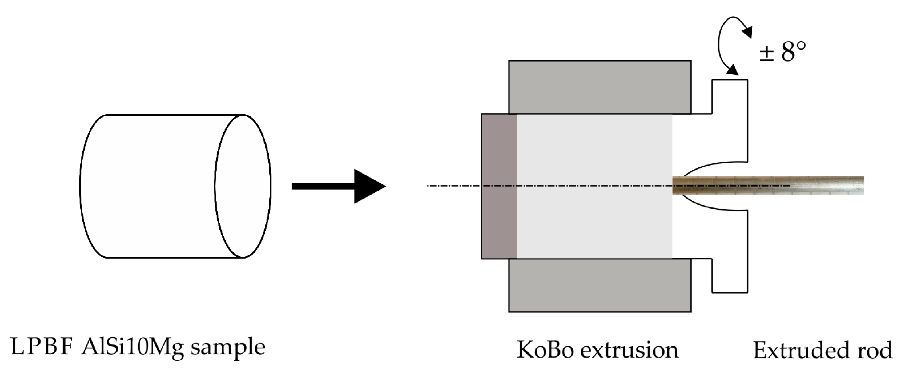
- As-built samples subjected to KoBo extrusion.
- Punch speed of 0.2 mm/s;
- Die rotation angle of ±8°;
- Frequency of 5 Hz;
- Extrusion ratio λ = 225;
- Maximal measured temperature close to the extrusion die (~280 °C);
- Sample cooling—room-temperature water.
3. Results
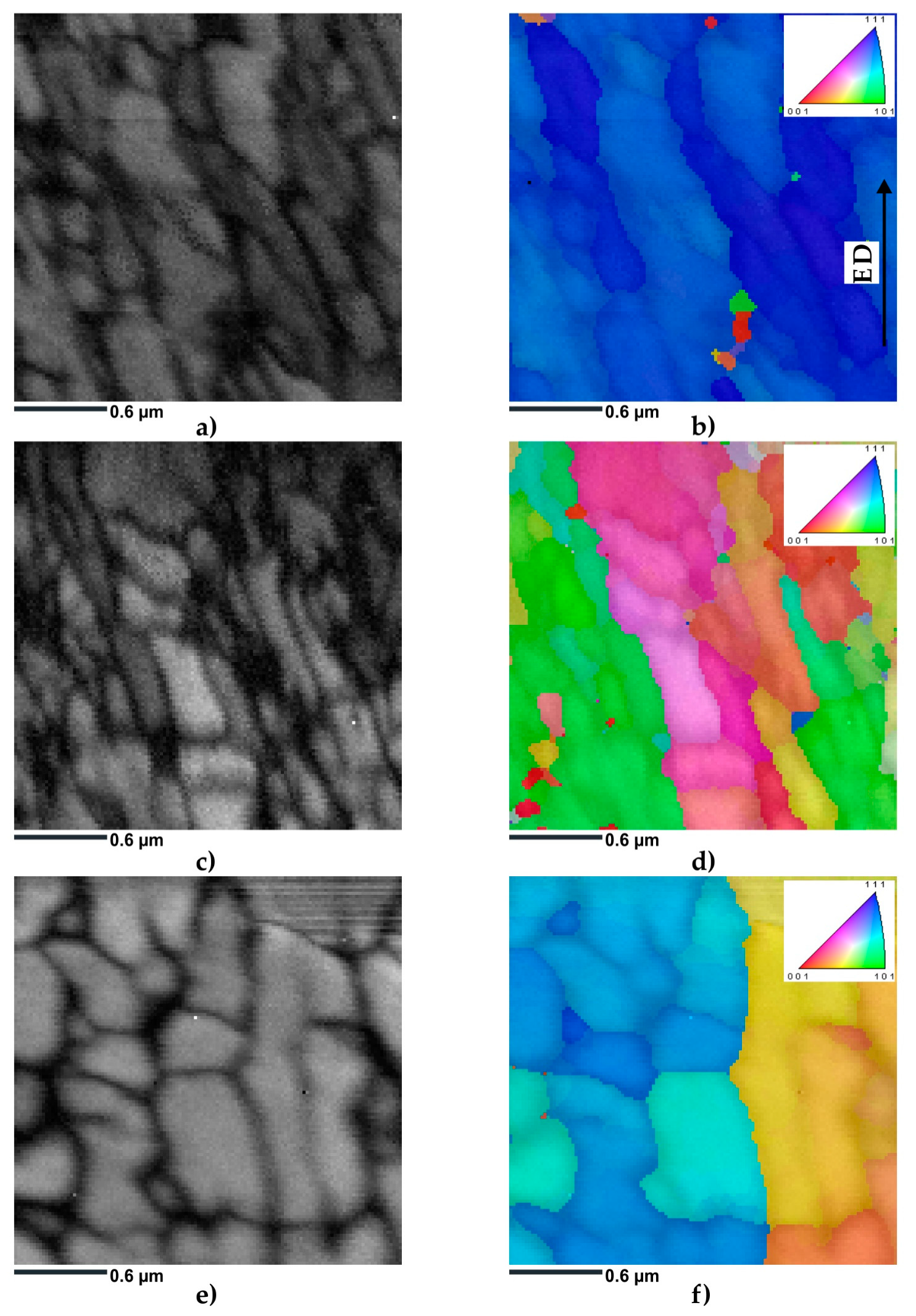
3.1. Microstructure Prior to Deformation
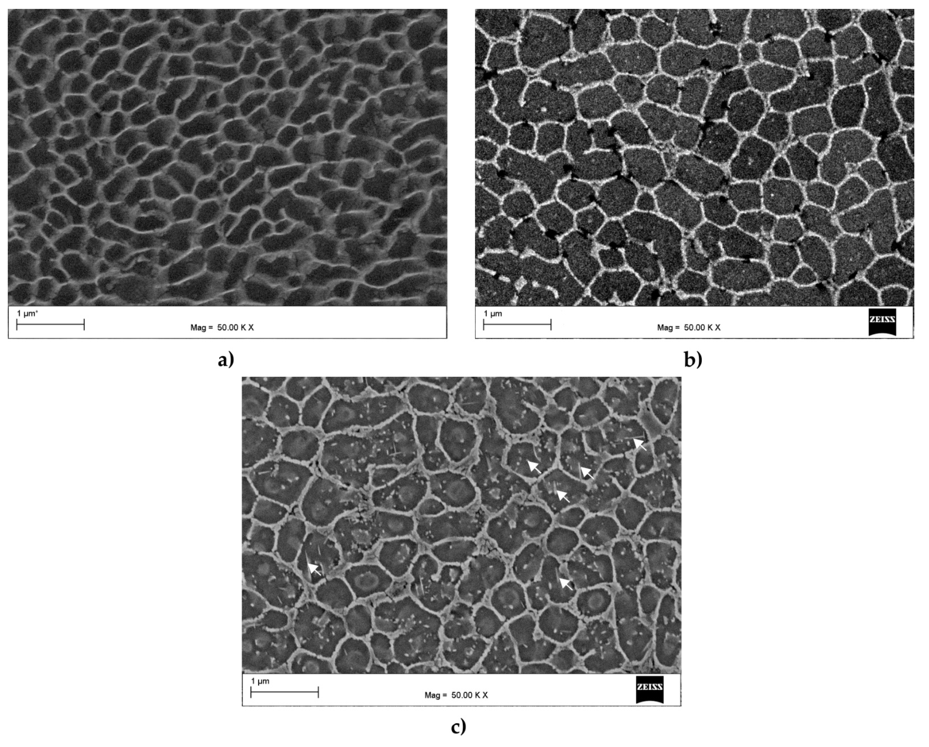
3.1.1. SEM Microstructures
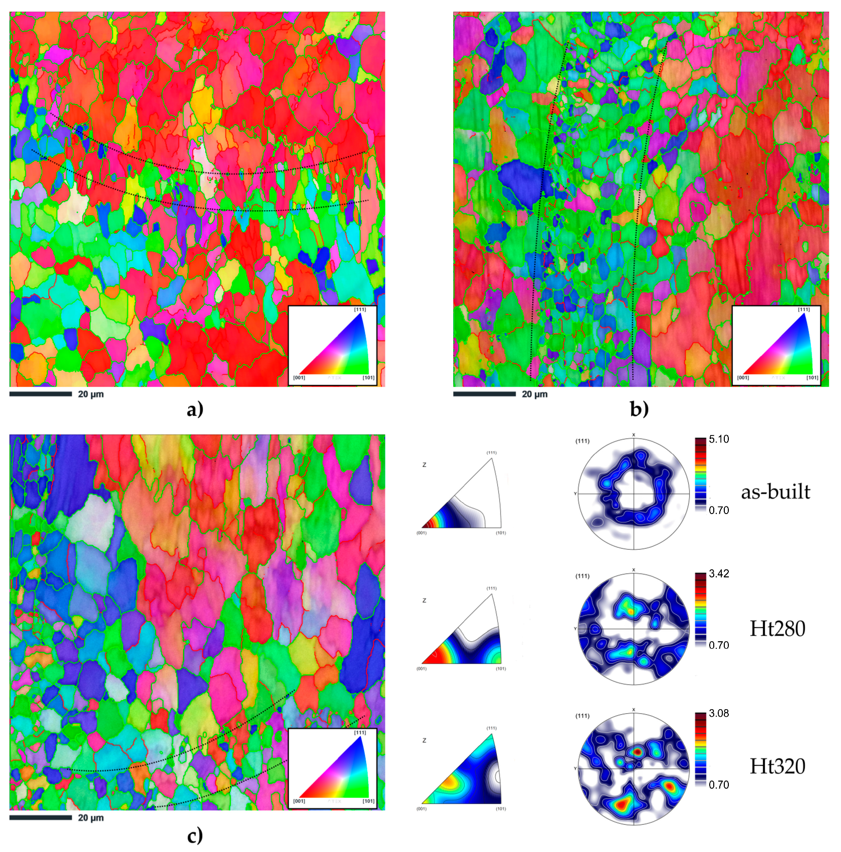
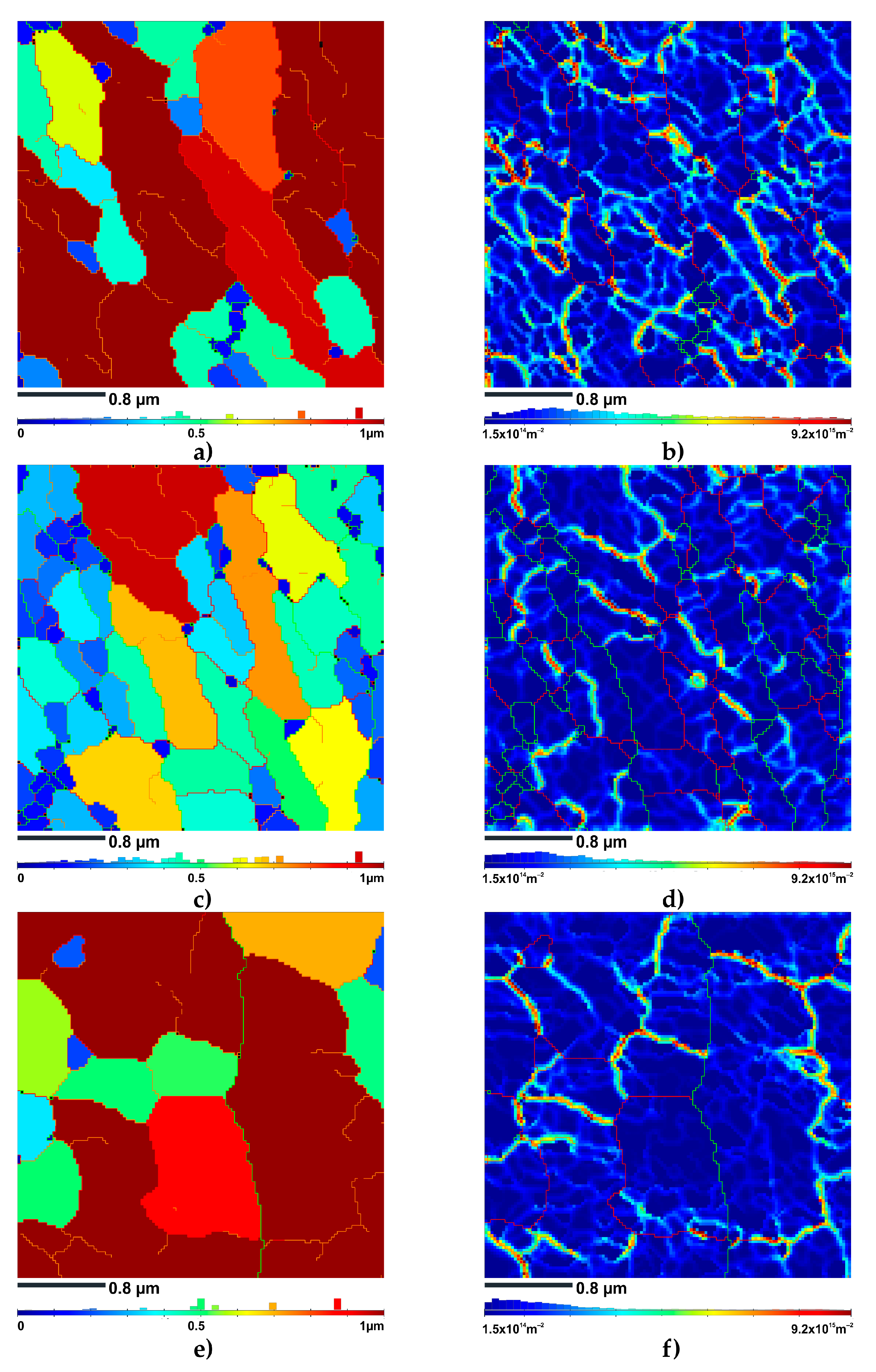
3.1.2. Grain Features and Crystallographic Orientation
3.2. ECAP-Processed Samples
3.2.1. Kikuchi Transmission Diffraction Analysis
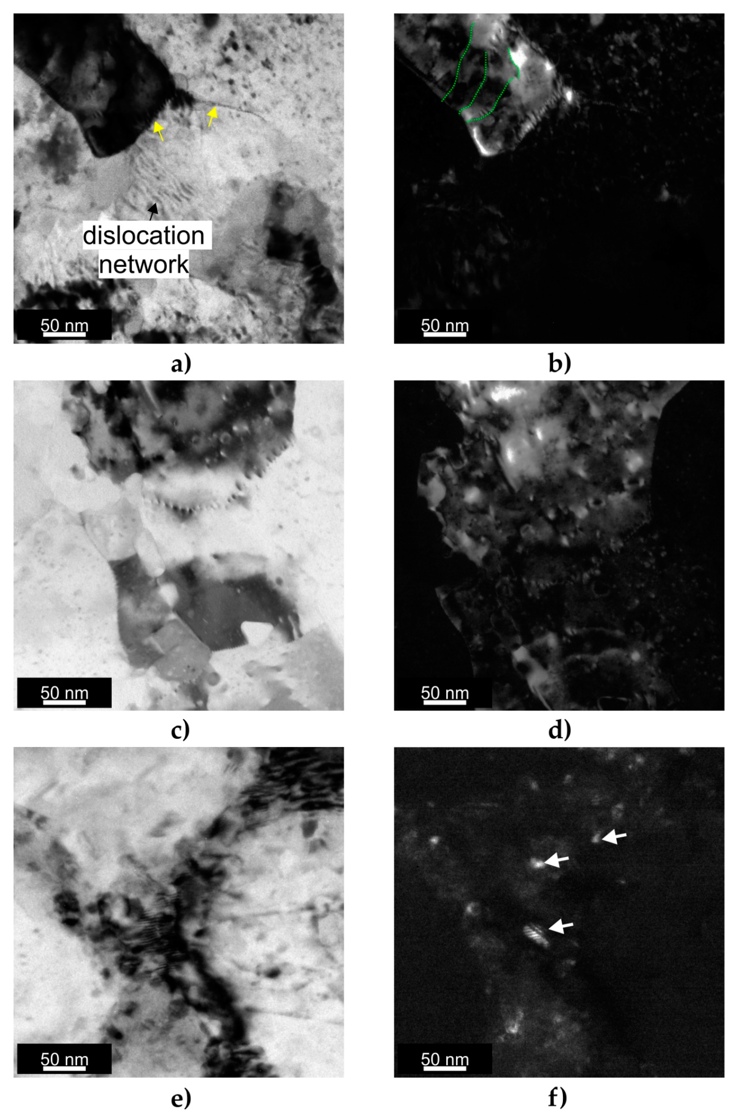
3.2.2. Transmission Electron Microscopy Analysis
3.3. Sample Subjected to Multi-Axial Forging
Transmission Electron Microscopy Analysis
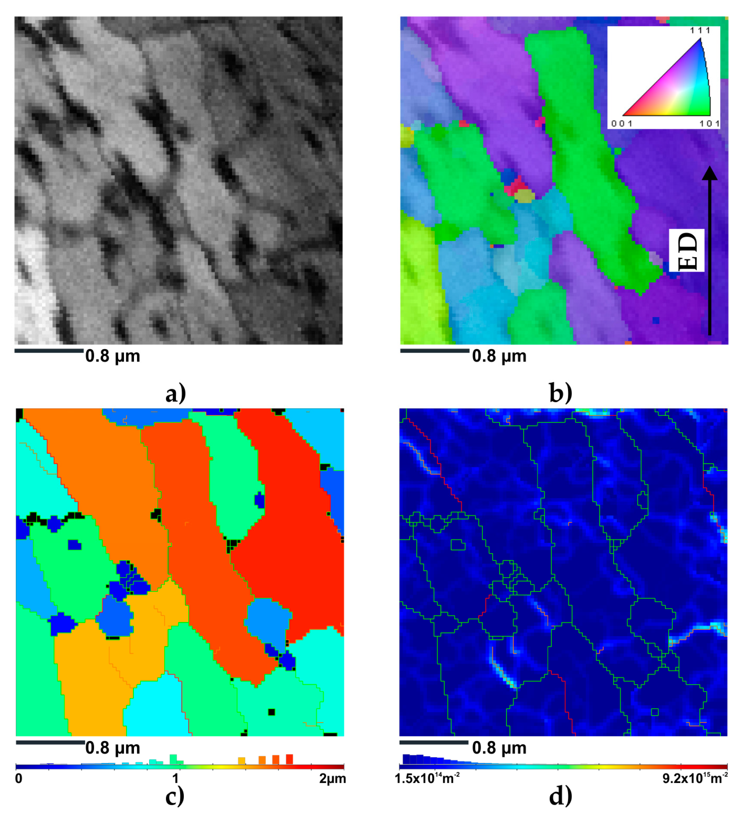
3.4. KoBo Sample
3.4.1. Transmission Kikuchi Diffraction Analysis
3.4.2. Transmission Electron Microscopy Analysis
4. Conclusions
- The average grain size increased from ~0.3 to ~0.7 after ECAP processing in the temperature range of 100 °C–200 °C.
- The substantial enhancements in spatial resolution facilitated by TKD allowed for the revelation and characterization of a nanoscale GND network that compensated for the low lattice curvature in the ECAP-processed samples.
- The multi-axial forging resulted in the formation of the finest subgrain size. It was revealed that the lamellar subgrains were subdivided by a nanoband structure.
- The KoBo process resulted in the fabrication of an almost dislocation-free microstructure with an average grain size of approx. 0.77 µm.
- The KoBo-processed sample exhibited a lower geometrically necessary dislocation density than the ECAP-processed samples.
- The results of the microstructural investigations presented in this article indicated that the MAF was the most promising method for the preparation of UFG AlSi10Mg samples.
Author Contributions
Funding
Institutional Review Board Statement
Informed Consent Statement
Data Availability Statement
Conflicts of Interest
References
- Votano, J.; Parham, M.; Hall, L. Hanbook of Aluminum: Volume 2: Alloy Production and Material Manufacturing; CRC Press: Boca Raton, FL, USA, 2004; pp. 1–731. [Google Scholar]
- Chiu, T.M.; Zhang, C.; Zhao, D.; Yadav, D.; Xie, K.Y.; Elwany, A.; Castaneda, H. Interface stability of laser powder-bed-fused AlSi12 under simulated atmospheric conditions. Corros. Sci. 2020, 175, 108861. [Google Scholar] [CrossRef]
- Zhou, L.; Mehta, A.; Schulz, E.; McWilliams, B.; Cho, K.; Sohn, Y. Microstructure, precipitates and hardness of selectively laser melted AlSi10Mg alloy before and after heat treatment. Mater. Charact. 2018, 143, 5–17. [Google Scholar] [CrossRef]
- Hyer, H.; Zhou, L.; Mehta, A.; Park, S.; Huynh, T.; Song, S.; Bai, Y.; Cho, K.; McWilliams, B.; Sohn, Y. Composition-dependent solidification cracking of aluminum-silicon alloys during laser powder bed fusion. Acta Mater. 2021, 208, 116698. [Google Scholar] [CrossRef]
- Eom, Y.S.; Park, J.M.; Choi, J.-W.; Seong, D.-J.; Joo, H.; Jo, Y.C.; Kim, K.T.; Yu, J.H.; Son, I. Fine-tuning of mechanical properties of additively manufactured AlSi10Mg alloys by controlling the microstructural heterogeneity. J. Alloys Compd. 2023, 956, 170348. [Google Scholar] [CrossRef]
- Fite, J.; Eswarappa Prameela, S.; Slotwinski, J.; Weihs, T.P. Enhanced mechanical properties by eutectic cells in AlSi10Mg—A promising paradigm for strengthening aluminum in additive manufacturing. Mater. Charact. 2023, 204, 113179. [Google Scholar] [CrossRef]
- Zhao, L.; Song, L.; Santos Macías, J.G.; Zhu, Y.; Huang, M.; Simar, A.; Li, Z. Review on the correlation between microstructure and mechanical performance for laser powder bed fusion AlSi10Mg. Addit. Manuf. 2022, 56, 102914. [Google Scholar] [CrossRef]
- Wang, P.; Rabori, A.S.; Dong, Q.; Ravkov, L.; Balogh, L.; Fallah, V. The role of cellular structure, non-equilibrium eutectic phases and precipitates on quasi-static strengthening mechanisms of as-built AlSi10Mg parts 3D printed via laser powder bed fusion. Mater. Charact. 2023, 198, 112730. [Google Scholar] [CrossRef]
- Snopiński, P.; Matus, K.; Tatiček, F.; Rusz, S. Overcoming the strength-ductility trade-off in additively manufactured AlSi10Mg alloy by ECAP processing. J. Alloys Compd. 2022, 918, 165817. [Google Scholar] [CrossRef]
- Salandari-Rabori, A.; Fallah, V. Heterogeneity of deformation, shear band formation and work hardening behavior of as-printed AlSi10Mg via laser powder bed fusion. Mater. Sci. Eng. A 2023, 866, 144698. [Google Scholar] [CrossRef]
- Salandari-Rabori, A.; Diak, B.J.; Fallah, V. Dislocation-obstacle interaction evolution in rate dependent plasticity of AlSi10Mg as-built microstructure by laser powder bed fusion. Mater. Sci. Eng. A 2022, 857, 144043. [Google Scholar] [CrossRef]
- Salandari Rabori, A.; Fallah, V. Room temperature strain rate sensitivity of as-built 3D printed AlSi10Mg by laser powder bed fusion. Mater. Lett. 2022, 320, 132395. [Google Scholar] [CrossRef]
- Fiocchi, J.; Biffi, C.A.; Colombo, C.; Vergani, L.M.; Tuissi, A. Ad Hoc Heat Treatments for Selective Laser Melted Alsi10mg Alloy Aimed at Stress-Relieving and Enhancing Mechanical Performances. JOM 2020, 72, 1118–1127. [Google Scholar] [CrossRef]
- Li, D.; Qin, R.; Xu, J.; Chen, B.; Niu, X. Effect of heat treatment on AlSi10Mg lattice structure manufactured by selective laser melting: Microstructure evolution and compression properties. Mater. Charact. 2022, 187, 111882. [Google Scholar] [CrossRef]
- Hirata, T.; Kimura, T.; Nakamoto, T. Effects of hot isostatic pressing and internal porosity on the performance of selective laser melted AlSi10Mg alloys. Mater. Sci. Eng. A 2020, 772, 138713. [Google Scholar] [CrossRef]
- Zhang, H.; Li, C.; Yao, G.; Zhang, Y. Hot isostatic pressing of laser powder-bed-fused 304L stainless steel under different temperatures. Int. J. Mech. Sci. 2022, 226, 107413. [Google Scholar] [CrossRef]
- Zhong, Y.; Liu, L.; Wikman, S.; Cui, D.; Shen, Z. Intragranular cellular segregation network structure strengthening 316L stainless steel prepared by selective laser melting. J. Nucl. Mater. 2016, 470, 170–178. [Google Scholar] [CrossRef]
- Maamoun, A.; Elbestawi, M.; Veldhuis, S. Influence of Shot Peening on AlSi10Mg Parts Fabricated by Additive Manufacturing. J. Manuf. Mater. Process. 2018, 2, 40. [Google Scholar] [CrossRef]
- Santos Macías, J.G.; Elangeswaran, C.; Zhao, L.; Van Hooreweder, B.; Adrien, J.; Maire, E.; Buffière, J.-Y.; Ludwig, W.; Jacques, P.J.; Simar, A. Ductilisation and fatigue life enhancement of selective laser melted AlSi10Mg by friction stir processing. Scr. Mater. 2019, 170, 124–128. [Google Scholar] [CrossRef]
- Xing, X.; Duan, X.; Jiang, T.; Wang, J.; Jiang, F. Ultrasonic peening treatment used to improve stress corrosion resistance of AlSi10Mg components fabricated using selective laser melting. Metals 2019, 9, 103. [Google Scholar] [CrossRef]
- Maleki, E.; Bagherifard, S.; Unal, O.; Jam, A.; Shao, S.; Guagliano, M.; Shamsaei, N. Superior effects of hybrid laser shock peening and ultrasonic nanocrystalline surface modification on fatigue behavior of additive manufactured AlSi10Mg. Surf. Coat. Technol. 2023, 463, 129512. [Google Scholar] [CrossRef]
- Hosseinzadeh, A.; Radi, A.; Richter, J.; Wegener, T.; Sajadifar, S.V.; Niendorf, T.; Yapici, G.G. Severe plastic deformation as a processing tool for strengthening of additive manufactured alloys. J. Manuf. Process. 2021, 68, 788–795. [Google Scholar] [CrossRef]
- Yusuf, S.M.; Hoegden, M.; Gao, N. Effect of sample orientation on the microstructure and microhardness of additively manufactured AlSi10Mg processed by high-pressure torsion. Int. J. Adv. Manuf. Technol. 2020, 106, 4321–4337. [Google Scholar] [CrossRef]
- Han, J.-K.; Liu, X.; Lee, I.; Kuzminova, Y.O.; Evlashin, S.A.; Liss, K.-D.; Kawasaki, M. Structural evolution during nanostructuring of additive manufactured 316L stainless steel by high-pressure torsion. Mater. Lett. 2021, 302, 130364. [Google Scholar] [CrossRef]
- Langdon, T.G. The principles of grain refinement in equal-channel angular pressing. Mater. Sci. Eng. A 2007, 462, 3–11. [Google Scholar] [CrossRef]
- Liu, M.; Roven, H.J.; Liu, X.; Murashkin, M.; Valiev, R.Z.; Ungár, T.; Balogh, L. Grain refinement in nanostructured Al-Mg alloys subjected to high pressure torsion. J. Mater. Sci. 2010, 45, 4659–4664. [Google Scholar] [CrossRef]
- Reza Toroghinejad, M.; Ashrafizadeh, F.; Jamaati, R. On the use of accumulative roll bonding process to develop nanostructured aluminum alloy 5083. Mater. Sci. Eng. A 2013, 561, 145–151. [Google Scholar] [CrossRef]
- Orlov, D.; Beygelzimer, Y.; Synkov, S.; Varyukhin, V.; Tsuji, N.; Horita, Z. Plastic flow, structure and mechanical properties in pure Al deformed by twist extrusion. Mater. Sci. Eng. A 2009, 519, 105–111. [Google Scholar] [CrossRef]
- Saxl, I.; Kalousová, A.; Ilucová, L.; Sklenička, V. Grain and subgrain boundaries in ultrafine-grained materials. Mater. Charact. 2009, 60, 1163–1167. [Google Scholar] [CrossRef]
- Ebrahimi, M.; Wang, Q.; Attarilar, S. A comprehensive review of magnesium-based alloys and composites processed by cyclic extrusion compression and the related techniques. Prog. Mater. Sci. 2023, 131, 101016. [Google Scholar] [CrossRef]
- Song, X.; Wang, L.; Wang, R.; Liu, Y. Effects of annealing on microstructure evolution and mechanical properties of constrained groove pressed pure titanium. Mater. Sci. Eng. A 2022, 831, 142245. [Google Scholar] [CrossRef]
- Zhang, L.; Ren, R.; Ren, J.; Liu, Y.; Liao, W.; Li, T.; Liu, C.; Wang, Q. Effects of cyclic closed-die forging on the microstructural evolution and mechanical properties of SiC/AZ91D nanocomposites. Int. J. Mod. Phys. B 2022, 36, 2240066. [Google Scholar] [CrossRef]
- Muñoz, J.A. Hot plastic behavior of an ultrafine-grained aluminum alloy fabricated by laser powder bed fusion and equal channel angular pressing. Superplast. Adv. Mater. 2023, 32, 330. [Google Scholar]
- Zhang, X.; Huang, L.K.; Zhang, B.; Chen, Y.Z.; Liu, F. Microstructural evolution and strengthening mechanism of an Al–Si–Mg alloy processed by high-pressure torsion with different heat treatments. Mater. Sci. Eng. A 2020, 794, 139932. [Google Scholar] [CrossRef]
- Park, J.M.; Asghari-Rad, P.; Zargaran, A.; Bae, J.W.; Moon, J.; Kwon, H.; Choe, J.; Yang, S.; Yu, J.-H.; Kim, H.S. Nano-scale heterogeneity-driven metastability engineering in ferrous medium-entropy alloy induced by additive manufacturing. Acta Mater. 2021, 221, 117426. [Google Scholar] [CrossRef]
- Snopiński, P.; Woźniak, A.; Pagáč, M. Microstructural Evolution, Hardness, and Strengthening Mechanisms in SLM AlSi10Mg Alloy Subjected to Equal-Channel Angular Pressing (ECAP). Materials 2021, 14, 7598. [Google Scholar] [CrossRef]
- Yaru, L.; Tiejun, M.; Tounan, J.; Bo, Z.; Le, Y.; Wenhang, Y.; Hanguang, F. Aging temperature effects on microstructure and mechanical properties for additively manufactured AlSi10Mg. Mater. Sci. Technol. 2023, 39, 1223–1236. [Google Scholar] [CrossRef]
- Prashanth, K.G.; Scudino, S.; Klauss, H.J.; Surreddi, K.B.; Löber, L.; Wang, Z.; Chaubey, A.K.; Kühn, U.; Eckert, J. Microstructure and mechanical properties of Al–12Si produced by selective laser melting: Effect of heat treatment. Mater. Sci. Eng. A 2014, 590, 153–160. [Google Scholar] [CrossRef]
- Casati, R.; Nasab, M.H.; Coduri, M.; Tirelli, V.; Vedani, M. Effects of platform pre-heating and thermal-treatment strategies on properties of alsi10mg alloy processed by selective laser melting. Metals 2018, 8, 954. [Google Scholar] [CrossRef]
- Merino, J.; Ruvalcaba, B.; Varela, J.; Arrieta, E.; Murr, L.E.; Wicker, R.B.; Benedict, M.; Medina, F. Multiple, comparative heat treatment and aging schedules for controlling the microstructures and mechanical properties of laser powder bed fusion fabricated AlSi10Mg alloy. J. Mater. Res. Technol. 2021, 13, 669–685. [Google Scholar] [CrossRef]
- Girelli, L.; Tocci, M.; Conte, M.; Giovanardi, R.; Veronesi, P.; Gelfi, M.; Pola, A. Effect of the T6 heat treatment on corrosion behavior of additive manufactured and gravity cast AlSi10Mg alloy. Mater. Corros. 2019, 70, 1808–1816. [Google Scholar] [CrossRef]
- Xu, J.; Brodin, H.; Peng, R.L.; Luzin, V.; Moverare, J. Effect of heat treatment temperature on the microstructural evolution of CM247LC superalloy by laser powder bed fusion. Mater. Charact. 2022, 185, 111742. [Google Scholar] [CrossRef]
- Muñoz, J.A.; Pavlov, M.; Cheverikin, V.; Komissarov, A.; Gromov, A. Heterogeneity consequences on the mechanical and microstructural evolution of an AlSi11Cu alloy obtained by selective laser melting. Mater. Charact. 2021, 174, 110989. [Google Scholar] [CrossRef]
- Li, Z.; Li, Z.; Tan, Z.; Xiong, D.B.; Guo, Q. Stress relaxation and the cellular structure-dependence of plastic deformation in additively manufactured AlSi10Mg alloys. Int. J. Plast. 2020. [Google Scholar] [CrossRef]
- Ren, J.; Wang, R.; Feng, Y.; Peng, C.; Cai, Z. Hot deformation behavior and microstructural evolution of as-quenched 7055 Al alloy fabricated by powder hot extrusion. Mater. Charact. 2019, 156, 109833. [Google Scholar] [CrossRef]
- Nikulin, I.; Kaibyshev, R. The Effect of Temperature on Microstructure Evolution in a 7055 Aluminum Alloy Subjected to ECAP. Mater. Sci. Forum 2012, 715–716, 317–322. [Google Scholar] [CrossRef]
- Snopiński, P.; Hilšer, O.; Hajnyš, J. Tuning the defects density in additively manufactured fcc aluminium alloy via modifying the cellular structure and post-processing deformation. Mater. Sci. Eng. A 2023, 865, 144605. [Google Scholar] [CrossRef]
- Wu, G.; Tang, J.; Wang, N.; Cao, Y.; Luo, J.; Chen, Y. Effect of strain rate-induced microstructure on mechanical behavior of dual-phase steel. J. Mater. Res. Technol. 2022, 18, 2093–2103. [Google Scholar] [CrossRef]
- Conrad, H. Thermally activated deformation of metals. JOM 1964, 16, 582–588. [Google Scholar] [CrossRef]
- Ben, D.D.; Ma, Y.R.; Yang, H.J.; Meng, L.X.; Shao, X.H.; Liu, H.Q.; Wang, S.G.; Duan, Q.Q.; Zhang, Z.F. Heterogeneous microstructure and voids dependence of tensile deformation in a selective laser melted AlSi10Mg alloy. Mater. Sci. Eng. A 2020, 798, 140109. [Google Scholar] [CrossRef]
- Liu, M.; Zheng, R.; Xiao, W.; Li, J.; Li, G.; Peng, Q.; Ma, C. Bulk nanostructured Al–Si alloy with remarkable improvement in strength and ductility. Scr. Mater. 2021, 201, 113970. [Google Scholar] [CrossRef]
- Liu, Q.; Fang, L.; Xiong, Z.; Yang, J.; Tan, Y.; Liu, Y.; Zhang, Y.; Tan, Q.; Hao, C.; Cao, L.; et al. The response of dislocations, low angle grain boundaries and high angle grain boundaries at high strain rates. Mater. Sci. Eng. A 2021, 822, 141704. [Google Scholar] [CrossRef]
- Zhang, X.; Zhao, J.; Kang, G.; Zaiser, M. Geometrically necessary dislocations and related kinematic hardening in gradient grained materials: A nonlocal crystal plasticity study. Int. J. Plast. 2023, 163, 103553. [Google Scholar] [CrossRef]


| Samples | As-Built | HT280 | HT320 |
|---|---|---|---|
| Average grain size, µm (GTA = 2°) | 3.9 | 4.2 | 4.6 |
| fHAGBs, % | 79.8 | 86.4 | 86.3 |
| fLAGBs, % | 20.2 | 13.6 | 13.7 |
| SAMPLE | HT320E100 | HT320E130 | HT280E200 |
|---|---|---|---|
| ρGND | 1.35 × 10¹⁵ m−2 | 1.0 × 10¹⁵ m−2 | 9.67 × 10¹⁴ m−2 |
| fLAGBs, % | 88 | 54 | 16 |
| fHAGBs, % | 12 | 46 | 84 |
Disclaimer/Publisher’s Note: The statements, opinions and data contained in all publications are solely those of the individual author(s) and contributor(s) and not of MDPI and/or the editor(s). MDPI and/or the editor(s) disclaim responsibility for any injury to people or property resulting from any ideas, methods, instructions or products referred to in the content. |
© 2023 by the authors. Licensee MDPI, Basel, Switzerland. This article is an open access article distributed under the terms and conditions of the Creative Commons Attribution (CC BY) license (https://creativecommons.org/licenses/by/4.0/).
Share and Cite
Snopiński, P.; Matus, K.; Hilšer, O. Investigation of the Effects of Various Severe Plastic Deformation Techniques on the Microstructure of Laser Powder Bed Fusion AlSi10Mg Alloy. Materials 2023, 16, 7418. https://doi.org/10.3390/ma16237418
Snopiński P, Matus K, Hilšer O. Investigation of the Effects of Various Severe Plastic Deformation Techniques on the Microstructure of Laser Powder Bed Fusion AlSi10Mg Alloy. Materials. 2023; 16(23):7418. https://doi.org/10.3390/ma16237418
Chicago/Turabian StyleSnopiński, Przemysław, Krzysztof Matus, and Ondřej Hilšer. 2023. "Investigation of the Effects of Various Severe Plastic Deformation Techniques on the Microstructure of Laser Powder Bed Fusion AlSi10Mg Alloy" Materials 16, no. 23: 7418. https://doi.org/10.3390/ma16237418