Review

A Review of Ultrathin Piezoelectric Films

School of Physics and Electronics, Hunan University, Changsha 410082, China
*
Authors to whom correspondence should be addressed.
Materials 2023, 16(8), 3107; https://doi.org/10.3390/ma16083107
Submission received: 15 March 2023 / Revised: 11 April 2023 / Accepted: 13 April 2023 / Published: 14 April 2023

Abstract

:
Due to their high electromechanical coupling and energy density properties, ultrathin piezoelectric films have recently been intensively studied as key materials for the construction of miniaturized energy transducers, and in this paper we summarize the research progress. At the nanoscale, even a few atomic layers, ultrathin piezoelectric films have prominent shape anisotropic polarization, that is, in-plane polarization and out-of-plane polarization. In this review, we first introduce the in-plane and out-of-plane polarization mechanism, and then summarize the main ultrathin piezoelectric films studied at present. Secondly, we take perovskite, transition metal dichalcogenides, and Janus layers as examples to elaborate the existing scientific and engineering problems in the research of polarization, and their possible solutions. Finally, the application prospect of ultrathin piezoelectric films in miniaturized energy converters is summarized.

1. Introduction

Since the discovery and synthesis of piezoelectric materials, researchers have gradually realized that piezoelectric technology can be widely used in biomedicine [1,2,3], flexible electronic devices [4,5], flexible generators [6,7,8,9], ultrathin film vibrators [10], piezoelectric photoelectronic solar cells [11,12] and many other fields. Many kinds of piezoelectric materials have been reported to have high piezoelectric properties and high electromechanical coupling, such as epitaxial wurtzite ScxAl1-xN ultrathin films [13] and nanocomposite [14,15]. In addition, the premise of high performance, coupled with the principle of being green, environmentally friendly, safe and sustainable, calls for the emergence of a number of new materials; for instance, lead-free 0.5Ba(Zr0.2Ti0.8)O3–0.5(Ba0.7Ca0.3)TiO3 nanowire [16], lead-free perovskite [17] and lead-free nanocomposites [18].
Generally speaking, microscopically, potential piezoelectric materials only originate from materials with a non-centrosymmetric microstructure. The work of Gowoon Cheon et al. [19] describes 325 potential two-dimensional (2D) piezoelectric materials. They are not piezoelectric in the bulk phase but lack central symmetry in the monolayer. There are 32 crystal symmetry groups, among which 21 have broken central symmetry. Surprisingly, 20 of them have directly observed piezoelectric responses. Piezoelectric materials were first discovered in naturally occurring natural products (quartz crystals and Rochelle salt). Monocrystalline, polycrystalline and polymer materials with better piezoelectric properties were discovered or synthesized later [20]. The classification of piezoelectric materials is given in Figure 1. Grounding three different criteria, completely different classification results will be showed. Furthermore, each type of material uses several materials to illustrate [21,22]. Most importantly, our focus is on all the parts of the diagram marked blue, that is to say, the type of polarization is a key factor. In Section 3, in-plane and out-of-plane polarization will be introduced in more detail.
Nevertheless, previous attention and research has focused mainly on materials with broken central symmetry [23,24,25]. Recently, in the reporting of D.-S. Park et al. [26], the piezoelectric phenomenon was realized in a centrosymmetric oxide. Unlike other methods, this exciting breakthrough was achieved by regulating the inserted oxygen vacancy with an applied electric field. In this regard, it also provides a new way to induce piezoelectricity. Under the action of a direct current (DC) electric field, the degree of defect migration has been significantly improved, which is represented by the numerical leap of dielectric constant. As a result, the achievement leads to the ultra-high voltage electrical property of the film [27]. Xiaoqing Yang et al. also used the first-principles method to predict the longitudinal piezoelectric effect of the oxide family AO (A = Cd, Ba, Sr, Ca, Mg, etc.) under the action of biaxial strain [28]. After this, it was also proved experimentally that the piezoelectric constant is enhanced in the 2D limit [29]. At the macro scale, a strain with a particular large gradient is required to cause significant polarization in the material, whereas, at the nano scale, even a small strain can do so [30,31]. For example, for the star material MoS2 in the 2D monolayer, an independent monolayer material is obtained experimentally through various preparation methods, and its piezoelectric properties are characterized [32,33]. These works provide an experimental basis and proof for 2D ultrathin piezoelectricity. Additionally, the layer odd–even dependence of the piezoelectric response was also found [33].
Aiming to achieve more adjustable piezoelectricity, a new fabrication method of traditional 2D materials [34] has been developed. At the same time, large piezoelectric responses have been achieved in the Janus monolayer through first-principles calculations [35]. Typically, the effect of inducing vertical dipoles by breaking the symmetry of the out-of-plane structure caused this huge response [36]. Of course, this mechanism can also be applied to group-III chalcogenide monolayers, such as Ga2SSe, with both inversion breaking and specular symmetry [37], though they still remain thermodynamically stable. Very recently, with the continuous progress of scientific and technological means, Bohayra Mortazavi et al. realized the first-principles study of piezoelectricity on MA2Z4 (M = Cr, Mo, W; A = Si, Ge; Z = N, P) monolayer through machine learning [38]. It is enough to raise concerns about new types of ultrathin films. The unique excellent performance of this group can even have a certain competitiveness in various application fields (nanoelectronics, optoelectronics and energy conversion nanosystems) [39].
In this review, we first elaborate the basic working principle of the piezoelectric effect in Section 2, and discuss the piezoelectric properties of thin film materials. Additionally, we also observe that the intrinsic difference of polarization mechanism between thin film and bulk material lies in the difference of anisotropy. Afterwards, we find that there are layer thickness effects and odd–even effects in these materials that already have theoretical and experimental foundations. Hence, we also summarize the physical mechanism grounding the instance of MoS2 and hexagonal boron nitride (h-BN). Notably, the modes applied by the strain have the potential to induce novel quantum effects, which will be the focus of future research. In Section 3, we classify ultrathin piezoelectric films from an entirely different perspective from most of the previous reviews: ultrathin in-plane piezoelectric films and ultrathin out-of-plane piezoelectric films. Moreover, based on transition metal dichalcogenides (TMDs), Janus structure and novel ultrathin films, the piezoelectric polarization mechanism and modification methods are analyzed. For the purpose of helping the workers who are interested in ultrathin piezoelectric films to clarify the components and their respective characteristics, we compiled the details included in this review. Finally, in Section 4, we summarize the current research progress of ultrathin piezoelectric films and their applications in energy harvesting and conversion and point out that there are still unavoidable defects and limitations in the fabrication of 2D materials within the scope of current technology.

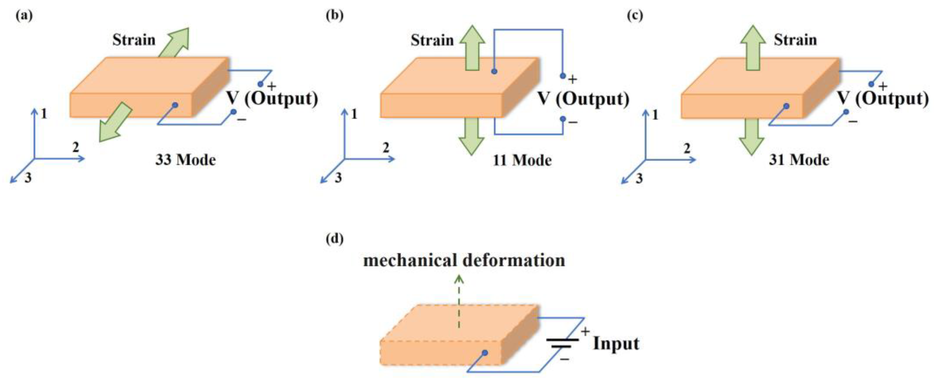
2. Piezoelectric Effect and Polarization Mechanisms

The piezoelectric effect results from the uneven distribution of ions in the crystal structure in some materials [40]. “Electric charge that accumulates in response to applied mechanical stress in materials that have non-centrosymmetric crystal structures” is defined as piezoelectricity [41]. A piezoelectric material is one that can achieve energy collection and conversion through the piezoelectric effect. Typically, the dipoles are randomly distributed in the crystal structure and call for an equilibrium state of electroneutrality on a macroscopic level. In these materials, though, electrons and holes move in opposite directions towards the metal-semiconductor interface due to a piezoelectric potential, which is generated by an external stimulus (polarization). The behavior by which the dipole tends to the same random direction is known as the piezoelectric polarization effect [42]. The connection between elasticity and electrical behavior is made successfully from then.
The piezoelectric effect can be modulated by regulating the interface properties of the electron transport as well as photoelectric properties [43]. The piezoelectric polarization effect can be divided into direct effect and inverse effect. The schematic diagram of the two working mechanisms is shown in Figure 2. Direct piezoelectric effects occur when the existing dipole balance in the crystal structure is disturbed due to the application of mechanical stress (stretching or compression) or vibrations. This disturbance results in an unbalanced distribution of charge, contributing to a surface charge density that is able to be captured by the electrode [44]. In this process, mechanical energy is converted to electric energy [45]. Conversely, the conversion of electrical energy into mechanical energy is an inverse piezoelectric effect. The whole process can be described as applying an electric field of a certain magnitude to the piezoelectric material. This effect causes a mechanical displacement within the material. The intrinsic equation of the two effects can be expressed as bellow [41]:
Direct   Effect :   D = d T + ε E
Inverse   Effect :   S = s T + d E
where T stands for the stress, d stands for the piezoelectric constant, S stands for the strain, D stands for the electric displacement, E stands for the electric field intensity, s stands for the mechanical flexibility, and ε stands for the dielectric constant of the material. The four piezoelectric coefficients d i j , e i j , g i j , h i j are expressed as [46]:
d i j = D i T j E = S j E i T e i j = D i S j E = T j E i S g i j = E i T j D = S j D i T h i j = E i S j D = T j D i S
these two terms after the equal sign correspond to direct and inverse piezoelectric effects, respectively.
Taking 2D TMDs as an example, the 2H phase structure has the symmetry of D 3 h space group. The in-plane and out-of-plane piezoelectric coefficients d 11 , d 31 and the elastic stiffness coefficients c 11 , c 31 satisfy the following relation [47]:
d 11 = e 11 C 11 C 12 ,   d 31 = e 31 C 11 + C 12 .
With regard to 2D materials with C 2 v space group symmetry, this relationship becomes [48]:
d 11 = e 11 C 22 e 12 C 12 C 11 C 22 C 12 2 ,   d 12 = e 12 C 11 e 11 C 12 C 11 C 22 C 12 2 .
Piezoelectric energy conversion and collection devices usually work with a direct piezoelectric effect, and the types are mainly the 33, 11 and 31 modes; these are shown in Figure 2a–c. In the 33 and 11 modes, the applied stress is in the same direction as the generated voltage, while in the 31 mode the applied stress is axial, and the voltage is vertical. The piezoelectric output is under the control of the operation mode. The 33 mode has excellent voltage output, while a superior manifestation aspect to high current output is found in the 31 mode [49,50]. On the other hand, the inverse piezoelectric effect is put into use in piezoelectric actuators, as shown in Figure 2d.
In various polarization mechanisms [51,52], it is common that the layer thickness effect and odd–even effect are reported [53]. As a matter of fact, they are attributed to changes in interlayer coupling and symmetry. Even layers samples have inversion symmetry, while odd layers samples destroy that. For example, direct and inverse piezoelectric effects have been experimentally confirmed in a single and few layers of MoS2. Nevertheless, in-plane piezoelectricity only exists in odd layers, and decreases rapidly with increasing number of layers. The reason for the phenomenon is that the response of the opposite direction layers is cancelled out. Meanwhile, any strain or electric field perpendicular to its surface will theoretically produce a zero piezoelectric response [30].

3. Piezoelectric Thin Films

The single layer of piezoelectric film is prepared experimentally, and the piezoelectricity constant is enhanced in the 2D limit [29,32,33]. These results and data mean the nano-scale ultrathin piezoelectric films are not only limited to theoretical calculation, but also signal a new era in the field of piezoelectric research. Table 1 and Table 2 show the piezoelectric coefficients of 2D piezoelectric film measured under the inverse piezoelectric effect and the direct piezoelectric effect, respectively. We find that several of these materials, such as ZnO, MoS2 and Zr2P2BrCl, show strong anisotropic piezoelectric polarization effects. This property is useful in that can be used to achieve different energy conversion effects by applying stretching or compression effects in different directions. In order to screen, distinguish and store different energy signals, it is often necessary to use anisotropic materials to design devices.

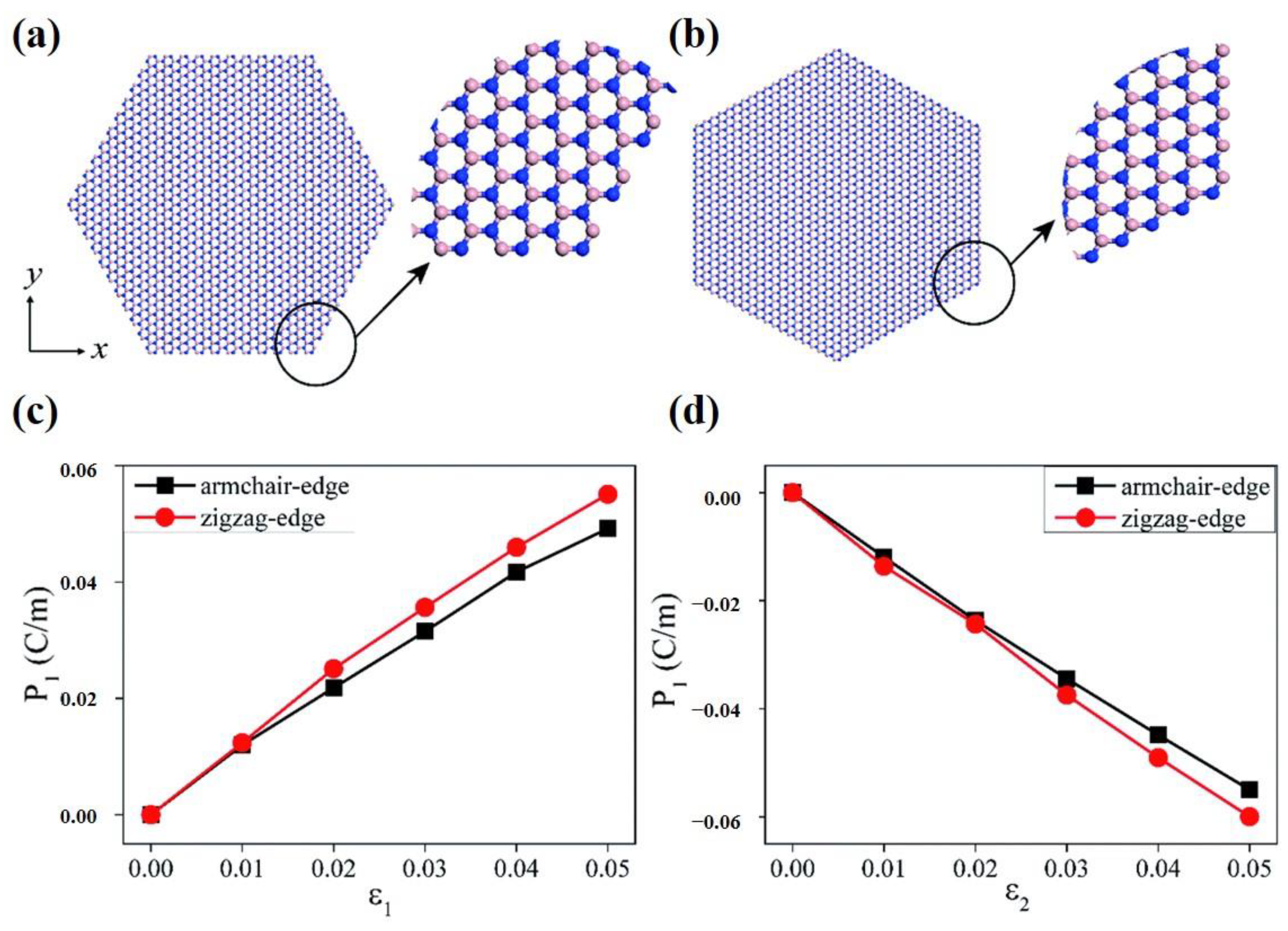
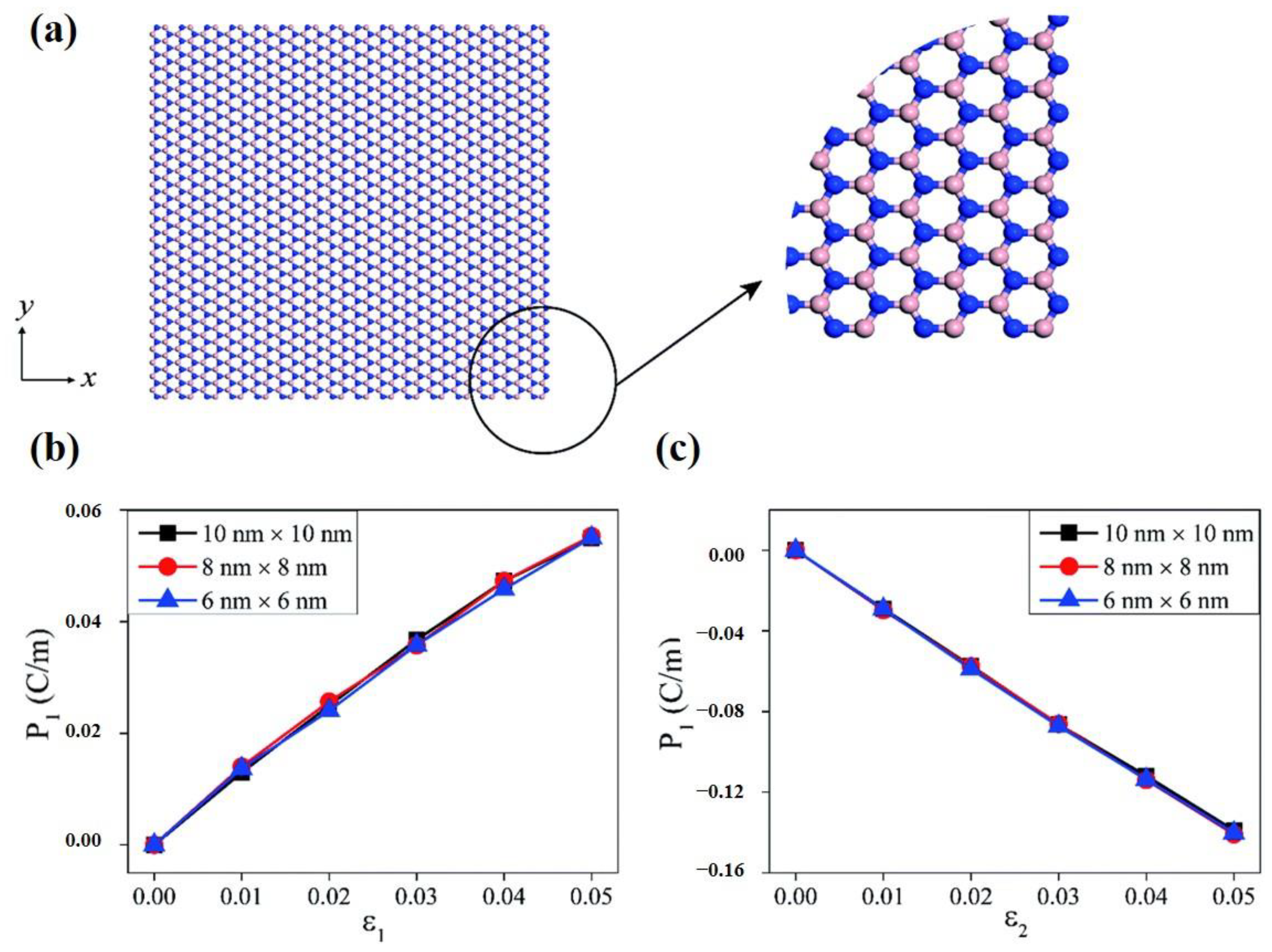
3.1. Ultrathin In-Plane Piezoelectric Films

With the development of energy equipment towards miniaturization, the critical scale of transducers needs to be reduced. The scale of ultrathin films in this review is defined to the nanometer scale. Most 2D materials have intrinsic piezoelectric polarization. We introduce the piezoelectric properties of TMDs, h-BN and black phosphorus (BP). A schematic of each of these structures is shown in Figure 3.
Ultrathin piezoelectric films are expected to be widely used as a result of their stress-electric conversion characteristics. Graphene has the longest history of study among 2D materials [103,104,105], and therefore was the material in which researchers initially tried to achieve the piezoelectric effect. Grounding the piezoelectric mechanism, the effect calls for the breaking of central symmetry. Swapnil Chandratre and Pradeep Sharma achieved the piezoelectric effect in 2D materials for the first time by digging triangular holes in graphene [106]. Shortly after, Mitchell T. Ong et al. chemically modified graphene with hydrogen and fluorine adsorbed on different position, and induced both in-plane and out-of-plane piezoelectric effects [107], as shown in Figure 4.
Ultrathin nanosheets of layered TMDs have tunable electronic structures, so as to be attractive for piezoelectric energy harvesting. TMDs can be represented as MX2 (M = Cr, Mo, W, Nb, Ta and X = S, Se, Te) [64]. Monolayer TMDs are constructed by a metal plane surrounded by two dichalcogenide planes [108]. Hexagonal structured monolayer TMDs are usually semiconductors and belong to D 3 h space group, the breaking of whose symmetry leads to piezoelectricity [109]. Duerloo et al. first predicted that 2D TMD materials are piezoelectric by the first-principles method [66]. MoS2 is the most widely studied TMD and it is worth going into more detail on. Monolayer MoS2 generates intrinsic electric dipoles due to the displacement of cationic Mo atoms and anionic S atoms when subjected to external strains. Additionally, the inherent electric dipoles lead to a voltage between the two sides of MoS2. The piezoelectric property of monolayer MoS2 is only restricted to the in-plane ( d 11 ) direction rather than the out-of-plane ( d 33 ) direction, since the symmetry feature along the vertical z-axis of monolayer MoS2 stays the same as in the initial state. Furthermore, Wu [71] and Zhu [33] et al. experimentally realized piezoelectricity in monolayer MoS2. Zhu et al. measured a piezoelectric coefficient of e 11 = 2.9 × 10⁻¹⁰ C m−1 in a free-standing single layer of MoS2. Additionally, they observed a finite and zero piezoelectric response in odd and even numbers of layers, respectively, which is in sharp contrast to bulk piezoelectric materials [33]. This is because the intrinsic difference of the polarization mechanism between thin film and bulk material relies on the difference of anisotropy. The measurement results are shown in Figure 5b. This is because symmetry is broken only in odd layers, while it is restored in even layers. The measurement method is shown in Figure 5a. The MoS2 film was indented with a scanning atomic force microscopy (AFM) probe, aiming to convert the in-plane stress to an out-of-plane force. The induced stress then changed the load on the tip and the curvature of the cantilever, which could be measured by the deflection of a laser beam [33]. Additionally, in the study of Wu et al., as shown in Figure 6, MoS2 was placed on a polyethylene terephthalate (PET) flexible substrate [71]. Uniaxial strain was applied to the MoS2 in the manner of mechanically bending the substrate. Therefore, periodic stretching and releasing of the substrate can generate piezoelectric outputs in external circuits with alternating polarity [71]. However, in principle, the exfoliated monolayer MoS2 lacks mechanical durability. Ju-Hyuck Lee et al. fabricated bilayer WSe2 with a mechanical durability of up to 0.95% of strain via turbostratic stacking [Figure 7a]. This form can increase the degrees of freedom in the bilayer symmetry and finally lead to non-centrosymmetry in the bilayers [Figure 7b] [72,110]. The density function theory (DFT) simulation results are shown in Figure 7c.
There has been a boom in research about in-plane piezoelectric 2D materials. Yang et al. calculated the piezoelectric coefficient of monolayer MX (M = Sn or Ge, X = Se or S) and found that the in-plane piezoelectric coefficient d11 of MX was the biggest among 2D materials [68]. This result is two orders of magnitude larger than that of routinely used piezoelectric semiconductors, such as ZnO and monolayer MoS2. This is because monolayer group IV monochalcogenides have a unique “puckered” C 2 v symmetry, as well as electronic structure.
Monolayer h-BN is a wide-band insulator with the same crystal structure as graphene. Unlike graphene, monolayer h-BN is piezoelectric due to the asymmetry introduced into the structure by the two sublattices (B and N). The elastic and piezoelectric effects were theoretically calculated using Born’s long-wavelength theory [111]. In 2020, Yang Nan et al. studied hexagonal boron nitride nanosheets through molecular dynamics simulations. Their simulation results indicated that the piezoelectric constants of boron nitride nanosheets depend very strongly on the macroscopic shape (Figure 8), while being nearly independent of the macroscopic size (Figure 9) [101]. In addition, when strain is applied to h-BN, some novel quantum effects, such as the quantum spin Hall phase [112], are born. These novel quantum effects, when combined with piezoelectric polarization effects, are bound to prompt researchers to ponder more interesting scientific questions.
Black phosphorus (BP) is a layered material that can be obtained by mechanical stripping. The piezoelectric properties of BP are demonstrated due to its non-centrosymmetric crystal structure [113]. In addition, surface-oxidization is an effective way to enhance the piezoelectricity of black phosphorene, since this method can break the structural symmetry. By first-principles methods, the calculated piezoelectric coefficients d 11 for surface-oxidized BP are manifested as 88.54 pm V−1, which is comparable to those of group-IV monochalcogenides and larger than that of 2D h-BN and MoS2 [77]. However, this method of stripping or traditional chemical and physical vapor deposition can likely introduce defects or other impurities, which can interfere with the results of the study. It is worth further consideration by researchers.
There are many kinds of means to control the properties of 2D materials, such as substitutional doping, staking, surface adatoms, or defects to break the centrosymmetry of pristine materials [114]. However, these strategies of regulating mainly affect the out-of-plane piezoelectric properties, which will be discussed later. The in-plane piezoelectric properties are little affected by these methods in principle, since the intrinsic asymmetry of materials is the factor most important to in-plane piezoelectric properties. Unconventionally, in 2022, Park et al. induced high levels of piezoelectricity in centrosymmetric oxides [26]. They used a DC electric field to rearrange the oxygen vacancies in the CeO2–x (CGO) thin film. The crystallographic symmetry was broken and piezoelectric effects were induced in centrosymmetric materials. The piezoelectricity is measured by applying an additional alternating current (AC) electric field (EAC). When the AC electric field is in the same direction as DC, oxygen vacancies are pushed up, which causes the material to expand. Conversely, when the AC electric field is in the opposite direction to DC, oxygen vacancies are pushed oppositely [27]. Their results show that the piezoelectric coefficients ( d 33 ) can reach up to nearly 200,000 pm V−1 at a frequency of 10 mHz under a DC electric field of 1 MV cm−1. This data is particularly significant, being two orders of magnitude larger than the ferroelectric oxide. They also discovered that the field-induced redistribution of oxygen vacancies could induce a cubic-to-tetragonal structural transition [26], as shown in Figure 10b. This inspired people to apply this method to more materials or look for new mechanisms to generate piezoelectricity.

3.2. Ultrathin Out-of-Plane Piezoelectric Films

With the systematic study of piezoelectricity in 2D materials, a variety of correlated novel piezoelectric devices have been successively fabricated in the field of energy harvesting, actuators, strain-tuned electronics, and optoelectronics. Most 2D materials, as shown in Figure 11a,b, have only in-plane piezoelectricity, which limits their applications in vertically integrated nanoelectromechanical systems [64]. Due to the limitation of external conditions and structural stability, it is difficult to make advanced functional devices with piezoelectric materials. Herein, Table 3 shows that the piezoelectric properties of common materials in different polarization directions are experimentally confirmed [54,115]. If 2D materials can obtain large out-of-plane piezoelectricity, they will be more widely used in a variety of piezoelectric applications. It has stimulated more and more research on innovative regulatory means, such as doping, construction of Janus structures and so on, because of the puzzle of how to obtain out-of-plane polarization.

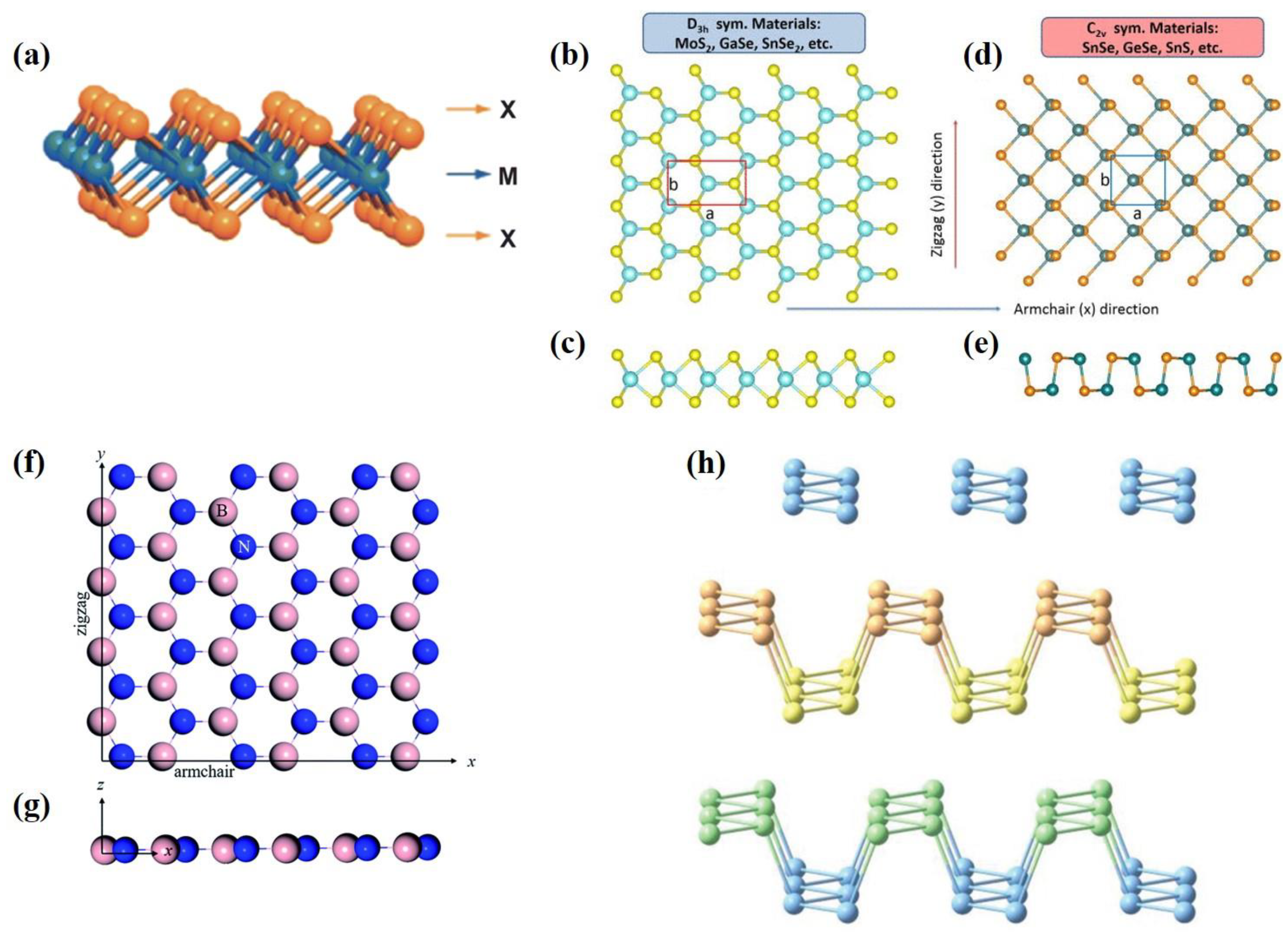
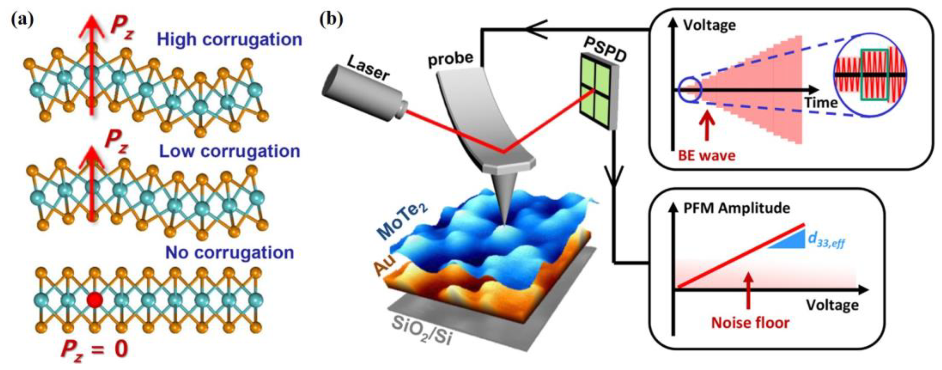
3.2.1. Out-of-Plane Piezoelectricity Obtained by Controlling Structures
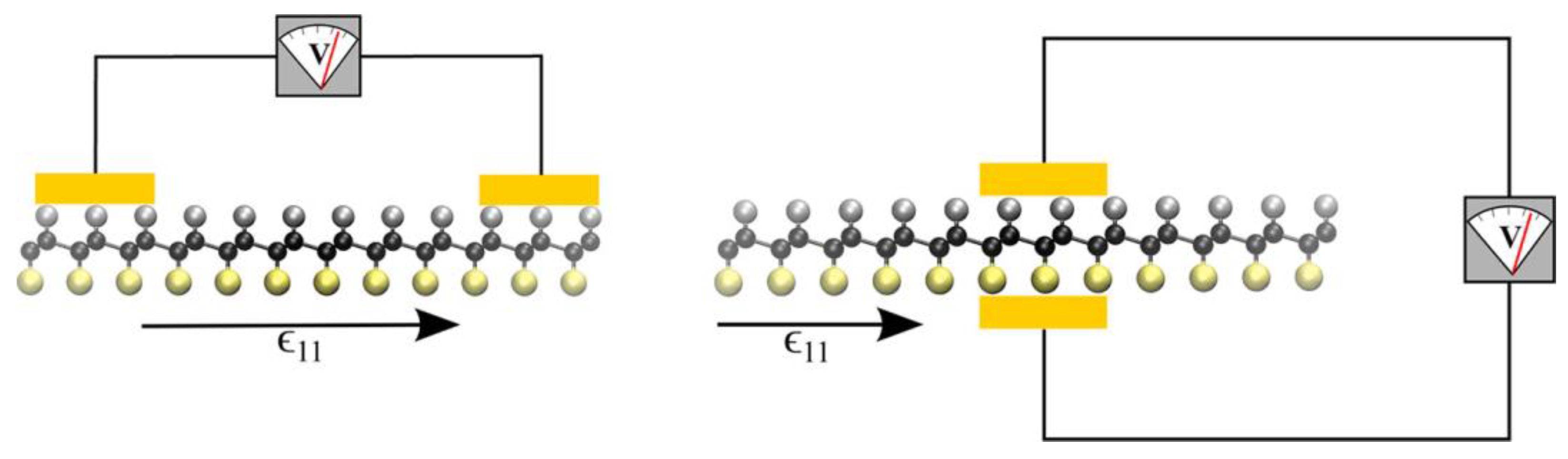
Out-of-plane piezoelectricity is usually obtained by controlling the crystal structure of the 2D materials, such as through defect engineering, deformation or doping. TMDs are ideal candidates as low-dimensional piezoelectric materials, owing to their structural non-centrosymmetry [33]. Due to in-plane inversion symmetry breaking, it was proved through experimental characterization and theoretical calculation that only intrinsic in-plane piezoelectricity exists in TMDs [64,66,117]. From this, breaking inversion symmetry in an out-of-plane direction is an efficient method to realize the out-of-plane piezoelectric polarization [115]. It is noted that the layered TMDs have the natural advantage of being established into out-of-plane piezoelectric samples through crystal structure transformation.

Deformation

While only in-plane piezoelectricity exists on the crystal symmetry, it is also possible to generate out-of-plane piezoelectricity by way of bringing strain to the gradient. The schematic diagram of different degrees of corrugation is shown in Figure 12a. As long as the 2D TMDs deform along the out-of-plane direction, the internal flexoelectricity polarization occurs along this axial direction. In this sense, the out-of-plane piezoelectricity of 2H phase MoTe2 can be modulated by either controlling the roughness of the substrate or the thickness of MoTe2 sample [118], as shown in Figure 12b.

Defect Engineering

Studies to date have demonstrated the possibility of generating an out-of-plane piezoelectric property in TMDs through defect engineering [114]. Still, it is a challenge to effectively modulate surface corrugation due to the limited modulation of substrate roughness or thickness. Thus comes the question of whether flexoelectricity can be generated at atomic scales or not. If so, out-of-plane piezoelectricity will be generated regardless of the roughness or thickness. The surface vacancy of a Te atom is generated by the thermal annealing process, which contributes to greater surface curvature and thus produces greater out-of-plane piezoelectricity [119].
Furthermore, out-of-plane piezoelectricity in TMDs with layered structure can be formed by using ion beams to engineer the defects. For instance, the formation of Te defects caused by helium ion beam irradiation on the multilayer MoTe2 actually leads to the out-of-plane piezoelectricity [120].

Doping

Chemical doping is also a new choice for obtaining out-of-plane piezoelectricity. Growing the material on the substrate can achieve this aim experimentally. The growth of graphene on SiO2 substrate causes the chemical interaction between graphene and SiO2 surface, thus realizing periodic doping. This interaction can induce band gap opening and dipole moment polarization of the graphene layer. Hence, it grants the material out-of-plane piezoelectricity [55]. In electronics manufacturing and energy harvesting applications, it is possible to use piezoelectric effects along the vertical direction in 2D TMDs.

3.2.2. Out-of-Plane Piezoelectricity in Janus Structures

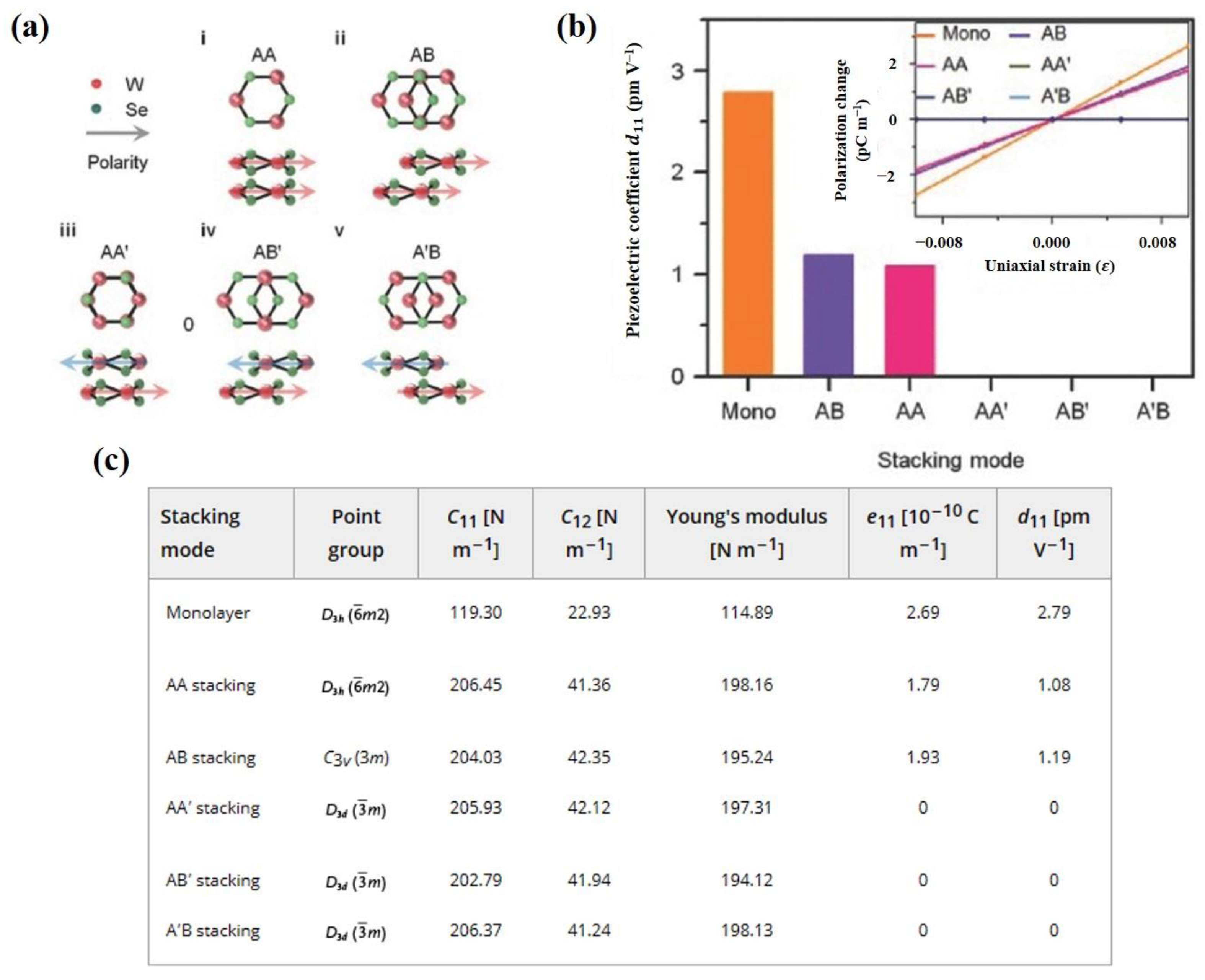
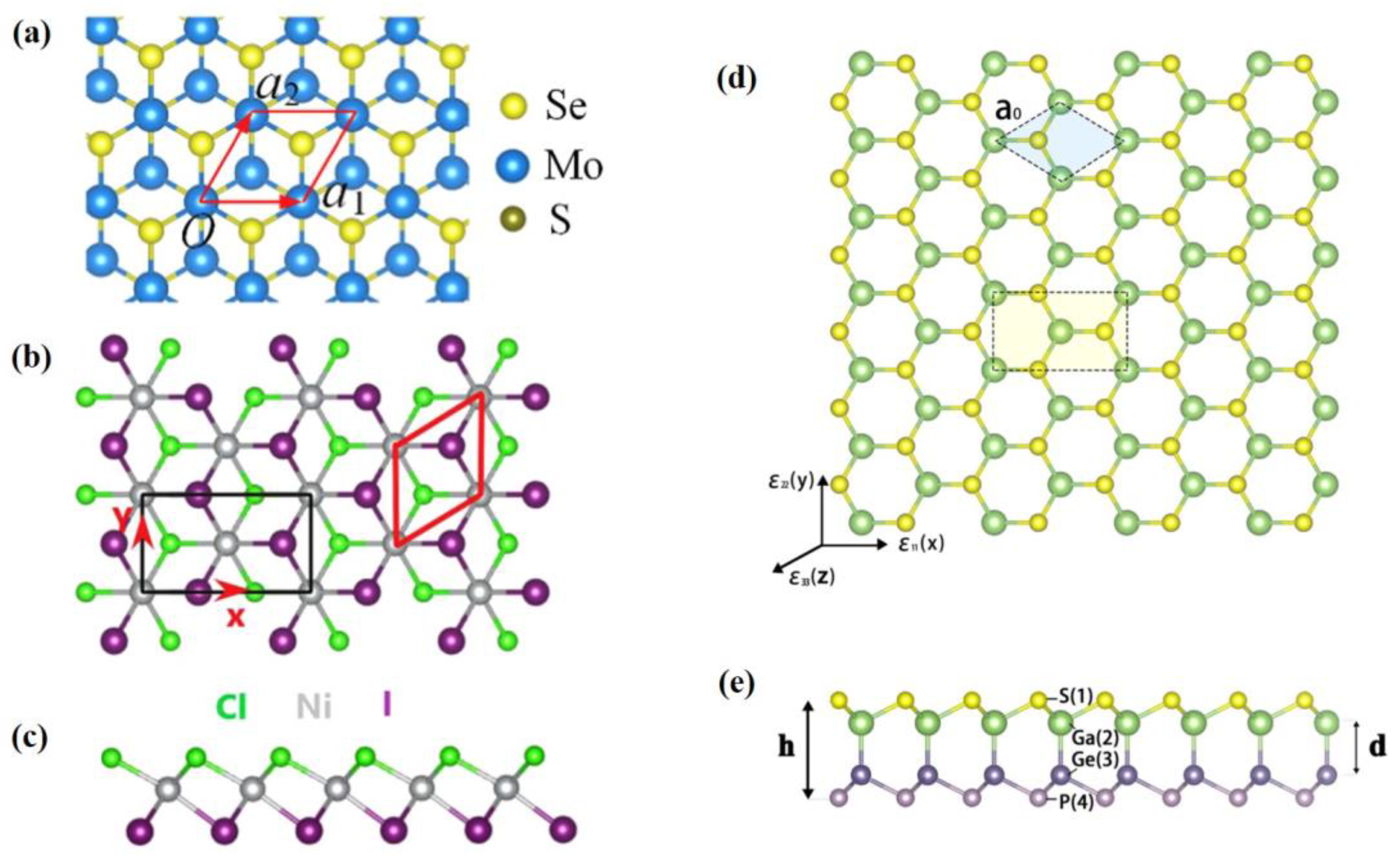
Conventional TMDs Janus Structures

Another atomic-scale approach has been proposed to induce out-of-plane piezoelectricity through constructing asymmetric TMD monolayers, known as conventional Janus structures. In addition to the most common MoSSe [65], NiXY (X/Y = Cl, Br, I; X Y) is also an example. The structure diagram is shown in Figure 13a–c. In this regard, NiXY is a novel piezoelectric ferromagnetic material with these two unique properties. These Janus monolayer materials, such as NiClBr and NiBrI, have strong in-plane as well as out-of-plane piezoelectricity. It is found that NiClI is a ferrovalley material with magnetic anisotropy, which is an ideal material for ultrathin piezoelectric devices [121].

Janus Derivatives

As a matter of fact, Janus can not only be based on TMDs, but also be built in typical single-layer structures with hexagonal primitive cells or a buckled honeycomb monolayer. A series of Janus derivatives are obtained by substituting atoms (GeP–GaS, SiP–AlS, and SnP–InS). The structure diagram is shown in Figure 13d,e. This type of structure lacks mirror symmetry, leading to a large out-of-plane piezoelectricity [123]. Single-layer SiN–GaS also exhibits considerable out-of-plane piezoelectricity [124]. Janus M2SeX (M = Ge, Sn; X = S, Te) have both large in-plane piezoelectric coefficients d 11 (up to 345.08 pm/V) and out-of-plane piezoelectric coefficients d 31 (up to 3.83 pm/V) [125]. As well as the larger surface piezoelectricity, Janus derivatives can also combine a variety of properties to offer opportunities for the manufacture of multifunctional devices. The research of the Janus structure of X2PAs monolayers shows that the out-of-plane piezoelectricity and flexible properties play an important part in improving the performance of multifunctional sensing and controlling of nanodevices [126]. The piezoelectric ferromagnetism material Fe2IX (X = Cl and Br) combines piezoelectricity, topological properties and ferromagnetism orders. In this sense, it provides a potential platform for multi-functional spintronic devices with a large gap and high TC (429 K) [127].
Janus materials also have tribo-piezoelectricity. The sliding of the in-plane interlayer leads to a remarkable enhancement in the vertical piezoelectricity aspect. In the process of Janus bilayer sliding, the tribological energy will convert into electrical energy. Hence, it brings a new perspective to creating new piezoelectric nanogenerators [122]. The construction of a Janus structure can fully demonstrate the modification of traditional 2D ultrathin films.

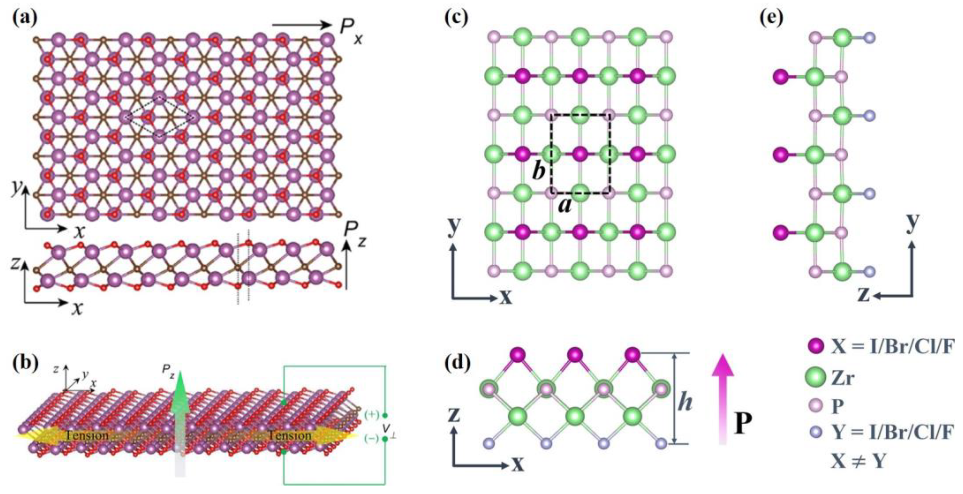
3.2.3. Out-of-Plane Piezoelectricity in Multi-Element Transition Metal Materials

If simple Janus can achieve structure asymmetry, can more complex structures do the same? The answer is, of course, yes. In 2D materials, a quantity of three- and four-membered compound monolayers are non-centrosymmetric, such as MXenes, lithium-based ternary chalcogenides and so on. A schematic of each of these structures is shown in Figure 14. Due to the uneven charge distribution caused by non-mirror symmetry, these multi-element transition metal materials have strong out of plane piezoelectricity.
Strikingly, M2CO2 (M = Sc, Y, La) has an in-plane piezoelectricity comparable to 2H-MoS2 as well as extraordinary out-of-plane piezoelectricity. The piezoelectric coefficient d 31 of Sc2CO2 MXene reaches 0.78 pm V−1. At 2.5% strain, 0.1 V vertical piezoelectric voltage can only be produced in such ultrathin Sc2CO2 monolayer [86]. Similarly, BiCrX3(X = S, Se, and Te) is a kind of piezoelectric ferromagnetism material with both in-plane and out-of-plane polarization at room temperature. Additionally, this is another breakthrough in high-performance piezoelectric materials [128].
The out-of-plane piezoelectric coefficients d 31 of 2D monolayer Li-based ternary chalcogenides LiMX2 (M = Al, Ga, In; X = S, Se, Te), such as LiAlSe2, LiGaTe2 and LiAlTe2, reach up to 0.61, 0.70 and 0.83 pm/V, respectively. This is owing to the unique double-buckled stacking structure of these LiMX2 monolayers [87]. Later, it was found that γ phase structure ( γ -LialS2 and γ -LialSe2) also has an excellent out-of-plane piezoelectric coefficient; even the number is twice as high as that of β phase structure [88]. When compared with the piezoelectric coefficients of other materials as shown in Figure 15, it is evident that the γ -LiMX2 structures are very promising materials for high-performance piezoelectric nanodevices.
Zr2P2BrCl monolayer is of particular interest for its ferroelasticity, controllable anisotropic properties along the in-plane direction and outstanding out-of-plane piezoelectricity. These monolayers have a strong out-of-plane piezoelectricity since the heterogeneous charge distribution results from its broken mirror symmetry. The piezoelectric coefficient d 33 = 129.705 pm V−1 of Zr2P2BrCl monolayer is actually significant, which is two orders of magnitude higher than MoSTe multilayers. It can even be a new alternate material for the design of memory devices, robot bionic skin or multipurpose nanodevices [89].
In addition to the materials mentioned above, the low-layer CuInP2S6 (CIPS) nanosheet also exhibits great performance. CIPS is a ferroelectric material with a high d 33 piezoelectric coefficient of 17.4 pm V−1. The data is superior to that of other reported 2D piezoelectric films to date. The intense out-of-plane piezoelectricity in the ultrathin CIPS contributes to the integration of nanoscale energy transducers, and thus eventually the production of nanogenerators [63]. A CIPS-based piezotronics device under compressive stress is shown in Figure 16.

4. Concluding Remarks

The intrinsic differences of ultrathin films, thick films and bulk materials regarding polarization due to gradually reduced anisotropy are explored in the first part of this review. When the thickness of material gradually decreases to several atoms thick, the effective piezoelectric polarization will enhance significantly. Secondly, several promising materials with strong anisotropy, such as ZnO, MoS2 and Zr2P2BrCl monolayer, are screened by summarizing the piezoelectric coefficient, polarization direction and preparation quality of the ultrathin films. It is noted that there are great difficulties in the acquisition and preparation of ultrathin piezoelectric films. The available methods have inevitable shortcomings and limitations, such as introducing a large number of defects, which is also a great challenge faced by the large family of 2D materials. Thirdly, based on the traditional piezoelectric hexagonal boron nitride structure, the effect of layer thickness, strain modes and sizes on polarization, and the novel quantum effects induced by it, such as topological state, quantum Hall effect, etc., are analyzed in detail. Particularly, the polarization mechanism of a few-atom-thick material is demonstrated by taking the symmetrically polarized monolayer TMDs as an example. In addition, to illustrate the construction and modification of a 2D piezoelectric material module, the Janus structure is taken as an example. Through this review, we have found that ultrathin piezoelectric films have made rapid progress and become a promising structure in the development of miniaturized energy conversion equipment.

Author Contributions

Conceptualization, B.L., Z.X. and H.L.; validation, B.L. and L.T.; investigation, B.L., Z.X. and H.L.; writing—original draft preparation, B.L., Z.X. and H.L.; writing—review and editing, L.T. and K.C.; supervision, L.T. and K.C.; funding acquisition, L.T. and K.C. All authors have read and agreed to the published version of the manuscript.

Funding

This research was funded by the National Natural Science Foundation of China (Grant Nos. 12074112 and 11974106).

Institutional Review Board Statement

Not applicable.

Informed Consent Statement

Not applicable.

Data Availability Statement

No new data were created or analyzed in this study.

Conflicts of Interest

The authors declare no conflict of interest.

References

  1. Surmenev, R.A.; Chernozem, R.V.; Pariy, I.O.; Surmeneva, M.A. A review on piezo- and pyroelectric responses of flexible nano- and micropatterned polymer surfaces for biomedical sensing and energy harvesting applications. Nano Energy 2021, 79, 105442. [Google Scholar] [CrossRef]
  2. Laurila, M.-M.; Peltokangas, M.; Montero, K.L.; Verho, J.; Haapala, M.; Oksala, N.; Vehkaoja, A.; Mäntysalo, M. Self-powered, high sensitivity printed e-tattoo sensor for unobtrusive arterial pulse wave monitoring. Nano Energy 2022, 102, 107625. [Google Scholar] [CrossRef]
  3. Wu, C.-W.; Ren, X.; Xie, G.; Zhou, W.-X.; Zhang, G.; Chen, K.-Q. Enhanced High-Temperature Thermoelectric Performance by Strain Engineering in BiOCl. Phys. Rev. Appl. 2022, 18, 014053. [Google Scholar] [CrossRef]
  4. Mariello, M.; Fachechi, L.; Guido, F.; De Vittorio, M. Conformal, Ultra-thin Skin-Contact-Actuated Hybrid Piezo/Triboelectric Wearable Sensor Based on AlN and Parylene-Encapsulated Elastomeric Blend. Adv. Funct. Mater. 2021, 31, 2101047. [Google Scholar] [CrossRef]
  5. Li, W.; Yang, T.; Liu, C.; Huang, Y.; Chen, C.; Pan, H.; Xie, G.; Tai, H.; Jiang, Y.; Wu, Y.; et al. Optimizing Piezoelectric Nanocomposites by High-Throughput Phase-Field Simulation and Machine Learning. Adv. Sci. 2022, 9, e2105550. [Google Scholar] [CrossRef] [PubMed]
  6. Lu, L.; Ding, W.; Liu, J.; Yang, B. Flexible PVDF based piezoelectric nanogenerators. Nano Energy 2020, 78, 105251. [Google Scholar] [CrossRef]
  7. Shepelin, N.A.; Glushenkov, A.M.; Lussini, V.C.; Fox, P.J.; Dicinoski, G.W.; Shapter, J.G.; Ellis, A.V. New developments in composites, copolymer technologies and processing techniques for flexible fluoropolymer piezoelectric generators for efficient energy harvesting. Energy Environ. Sci. 2019, 12, 1143–1176. [Google Scholar] [CrossRef]
  8. Yu, D.; Zheng, Z.; Liu, J.; Xiao, H.; Huangfu, G.; Guo, Y. Superflexible and Lead-Free Piezoelectric Nanogenerator as a Highly Sensitive Self-Powered Sensor for Human Motion Monitoring. Nano-Micro Lett. 2021, 13, 117. [Google Scholar] [CrossRef]
  9. Zhong, J.; Zhong, Q.; Zang, X.; Wu, N.; Li, W.; Chu, Y.; Lin, L. Flexible PET/EVA-based piezoelectret generator for energy harvesting in harsh environments. Nano Energy 2017, 37, 268–274. [Google Scholar] [CrossRef]
  10. Takeshita, T.; Nguyen, T.-V.; Zymelka, D.; Takei, Y.; Kobayashi, T. Mechanical characteristics of laminated film vibrator using an ultra-thin MEMS actuator. J. Micromech. Microeng. 2022, 32, 105001. [Google Scholar] [CrossRef]
  11. Michael, G.; Hu, G.; Zheng, D.; Zhang, Y. Piezo-phototronic solar cell based on 2D monochalcogenides materials. J. Phys. D Appl. Phys. 2019, 52, 204001. [Google Scholar] [CrossRef]
  12. Wu, W.; Wang, Z.L. Piezotronics and piezo-phototronics for adaptive electronics and optoelectronics. Nat. Rev. Mater. 2016, 1, 16031. [Google Scholar] [CrossRef]
  13. Casamento, J.; Chang, C.S.; Shao, Y.-T.; Wright, J.; Muller, D.A.; Xing, H.; Jena, D. Structural and piezoelectric properties of ultra-thin ScxAl1−xN films grown on GaN by molecular beam epitaxy. Appl. Phys. Lett. 2020, 117, 112101. [Google Scholar] [CrossRef]
  14. Yu, S.; Zhang, Y.; Yu, Z.; Zheng, J.; Wang, Y.; Zhou, H. PANI/PVDF-TrFE porous aerogel bulk piezoelectric and triboelectric hybrid nanogenerator based on in-situ doping and liquid nitrogen quenching. Nano Energy 2021, 80, 105519. [Google Scholar] [CrossRef]
  15. Shi, K.; Chai, B.; Zou, H.; Shen, P.; Sun, B.; Jiang, P.; Shi, Z.; Huang, X. Interface induced performance enhancement in flexible BaTiO3/PVDF-TrFE based piezoelectric nanogenerators. Nano Energy 2021, 80, 105515. [Google Scholar] [CrossRef]
  16. Zhou, Z.; Bowland, C.C.; Malakooti, M.H.; Tang, H.; Sodano, H.A. Lead-free 0.5Ba(Zr0.2Ti0.8)O3–0.5(Ba0.7Ca0.3)TiO3 nanowires for energy harvesting. Nanoscale 2016, 8, 5098–5105. [Google Scholar] [CrossRef]
  17. Zheng, T.; Wu, J.; Xiao, D.; Zhu, J. Recent development in lead-free perovskite piezoelectric bulk materials. Prog. Mater. Sci. 2018, 98, 552–624. [Google Scholar] [CrossRef]
  18. Jeong, C.K.; Park, K.-I.; Ryu, J.; Hwang, G.-T.; Lee, K.J. Large-Area and Flexible Lead-Free Nanocomposite Generator Using Alkaline Niobate Particles and Metal Nanorod Filler. Adv. Funct. Mater. 2014, 24, 2620–2629. [Google Scholar] [CrossRef]
  19. Cheon, G.; Duerloo, K.-A.N.; Sendek, A.D.; Porter, C.; Chen, Y.; Reed, E.J. Data Mining for New Two- and One-Dimensional Weakly Bonded Solids and Lattice-Commensurate Heterostructures. Nano Lett. 2017, 17, 1915–1923. [Google Scholar] [CrossRef]
  20. Mohith, S.; Upadhya, A.R.; Navin, K.P.; Kulkarni, S.M.; Rao, M. Recent trends in piezoelectric actuators for precision motion and their applications: A review. Smart Mater. Struct. 2020, 30, 013002. [Google Scholar] [CrossRef]
  21. Wang, J.; Cao, X.-H.; Zeng, Y.-J.; Luo, N.-N.; Tang, L.-M.; Chen, K.-Q. Excellent thermoelectric properties of monolayer MoS2-MoSe2 aperiodic superlattices. Appl. Surf. Sci. 2023, 612, 155914. [Google Scholar] [CrossRef]
  22. Jia, P.-Z.; Xie, Z.-X.; Deng, Y.-X.; Zhang, Y.; Tang, L.-M.; Zhou, W.-X.; Chen, K.-Q. High thermoelectric performance induced by strong anharmonic effects in monolayer (PbX)2 (X = S, Se, Te). Appl. Phys. Lett. 2022, 121, 043901. [Google Scholar] [CrossRef]
  23. He, R.; Wang, D.; Luo, N.; Zeng, J.; Chen, K.-Q.; Tang, L.-M. Nonrelativistic Spin-Momentum Coupling in Antiferromagnetic Twisted Bilayers. Phys. Rev. Lett. 2023, 130, 046401. [Google Scholar] [CrossRef] [PubMed]
  24. Yuan, Z.-L.; Sun, Y.; Wang, D.; Chen, K.-Q.; Tang, L.-M. A review of ultra-thin ferroelectric films. J. Phys. Condens. Matter 2021, 33, 403003. [Google Scholar] [CrossRef]
  25. Li, Q.; Chen, K.-Q.; Tang, L.-M. Large Valley Splitting in van der Waals Heterostructures with Type-III Band Alignment. Phys. Rev. Appl. 2020, 13, 014064. [Google Scholar] [CrossRef]
  26. Park, D.-S.; Hadad, M.; Riemer, L.M.; Ignatans, R.; Spirito, D.; Esposito, V.; Tileli, V.; Gauquelin, N.; Chezganov, D.; Jannis, D.; et al. Induced giant piezoelectricity in centrosymmetric oxides. Science 2022, 375, 653–657. [Google Scholar] [CrossRef]
  27. Li, F. Breaking symmetry for piezoelectricity. Science 2022, 375, 618–619. [Google Scholar] [CrossRef]
  28. Yang, X.; Liu, C.; Fang, L.; Su, T.; Hu, M.; Chen, Y.; Zhou, B.; Su, H.; Kong, X.; Bellaiche, L.; et al. Strain-induced ferroelectricity and piezoelectricity in centrosymmetric binary oxides. Phys. Rev. B 2022, 106, 064106. [Google Scholar] [CrossRef]
  29. Wu, T.; Zhang, H. Piezoelectricity in Two-Dimensional Materials. Angew. Chem. Int. Ed. 2015, 54, 4432–4434. [Google Scholar] [CrossRef]
  30. Brennan, C.J.; Ghosh, R.; Koul, K.; Banerjee, S.K.; Lu, N.; Yu, E.T. Out-of-Plane Electromechanical Response of Monolayer Molybdenum Disulfide Measured by Piezoresponse Force Microscopy. Nano Lett. 2017, 17, 5464–5471. [Google Scholar] [CrossRef]
  31. Cao, X.-H.; Wu, D.; Zeng, J.; Luo, N.-N.; Zhou, W.-X.; Tang, L.-M.; Chen, K.-Q. Controllable anisotropic thermoelectric properties in 2D covalent organic radical frameworks. Appl. Phys. Lett. 2021, 119, 263901. [Google Scholar] [CrossRef]
  32. Kim, S.K.; Bhatia, R.; Kim, T.-H.; Seol, D.; Kim, J.H.; Kim, H.; Seung, W.; Kim, Y.; Lee, Y.H.; Kim, S.-W. Directional dependent piezoelectric effect in CVD grown monolayer MoS 2 for flexible piezoelectric nanogenerators. Nano Energy 2016, 22, 483–489. [Google Scholar] [CrossRef]
  33. Zhu, H.; Wang, Y.; Xiao, J.; Liu, M.; Xiong, S.; Wong, Z.J.; Ye, Z.; Ye, Y.; Yin, X.; Zhang, X. Observation of piezoelectricity in free-standing monolayer MoS2. Nat. Nanotechnol. 2015, 10, 151–155. [Google Scholar] [CrossRef] [PubMed]
  34. Liu, D.; Zeng, J.; Jiang, X.; Tang, L.; Chen, K. Exact first-principles calculation reveals universal moiré potential in twisted two-dimensional materials. Phys. Rev. B 2023, 107, L081402. [Google Scholar] [CrossRef]
  35. Varjovi, M.J.; Yagmurcukardes, M.; Peeters, F.M.; Durgun, E. Janus two-dimensional transition metal dichalcogenide oxides: First-principles investigation of WXO monolayers with X = S, Se, and Te. Phys. Rev. B 2021, 103, 195438. [Google Scholar] [CrossRef]
  36. Lu, A.-Y.; Zhu, H.; Xiao, J.; Chuu, C.-P.; Han, Y.; Chiu, M.-H.; Cheng, C.-C.; Yang, C.-W.; Wei, K.-H.; Yang, Y.Y.P.; et al. Janus monolayers of transition metal dichalcogenides. Nat. Nanotechnol. 2017, 12, 744–749. [Google Scholar] [CrossRef] [Green Version]
  37. Guo, Y.; Zhou, S.; Bai, Y.; Zhao, J. Enhanced piezoelectric effect in Janus group-III chalcogenide monolayers. Appl. Phys. Lett. 2017, 110, 163102. [Google Scholar] [CrossRef]
  38. Mortazavi, B.; Javvaji, B.; Shojaei, F.; Rabczuk, T.; Shapeev, A.V.; Zhuang, X. Exceptional piezoelectricity, high thermal conductivity and stiffness and promising photocatalysis in two-dimensional MoSi2N4 family confirmed by first-principles. Nano Energy 2020, 82, 105716. [Google Scholar] [CrossRef]
  39. Safaei, M.; Sodano, H.A.; Anton, S.R. A review of energy harvesting using piezoelectric materials: State-of-the-art a decade later (2008–2018). Smart Mater. Struct. 2019, 28, 113001. [Google Scholar] [CrossRef]
  40. Das Mahapatra, S.; Mohapatra, P.C.; Aria, A.I.; Christie, G.; Mishra, Y.K.; Hofmann, S.; Thakur, V.K. Piezoelectric Materials for Energy Harvesting and Sensing Applications: Roadmap for Future Smart Materials. Adv. Sci. 2021, 8, e2100864. [Google Scholar] [CrossRef]
  41. Covaci, C.; Gontean, A. Piezoelectric Energy Harvesting Solutions: A Review. Sensors 2020, 20, 3512. [Google Scholar] [CrossRef] [PubMed]
  42. Li, F.; Shen, T.; Wang, C.; Zhang, Y.; Qi, J.; Zhang, H. Recent Advances in Strain-Induced Piezoelectric and Piezoresistive Effect-Engineered 2D Semiconductors for Adaptive Electronics and Optoelectronics. Nano-Micro Lett. 2020, 12, 106. [Google Scholar] [CrossRef] [PubMed]
  43. Lin, P.; Yan, X.; Li, F.; Du, J.; Meng, J.; Zhang, Y. Polarity-Dependent Piezotronic Effect and Controllable Transport Modulation of ZnO with Multifield Coupled Interface Engineering. Adv. Mater. Interfaces 2017, 4, 1600842. [Google Scholar] [CrossRef]
  44. Mishra, S.; Unnikrishnan, L.; Nayak, S.K.; Mohanty, S. Advances in Piezoelectric Polymer Composites for Energy Harvesting Applications: A Systematic Review. Macromol. Mater. Eng. 2019, 304, 1800463. [Google Scholar] [CrossRef] [Green Version]
  45. Zeng, Y.-J.; Liu, Y.-Y.; Pan, H.; Ding, Z.-K.; Zhou, W.-X.; Tang, L.-M.; Li, B.; Chen, K.-Q. Thermoelectric Conversion From Interface Thermophoresis and Piezoelectric Effects. Front. Phys. 2022, 10, 823284. [Google Scholar] [CrossRef]
  46. 176-1978; IEEE Standard on Piezoelectricity. IEEE: Piscatvie, NJ, USA, 1988.
  47. Li, W.; Li, J. Piezoelectricity in two-dimensional group-III monochalcogenides. Nano Res. 2015, 8, 3796–3802. [Google Scholar] [CrossRef] [Green Version]
  48. Hu, T.; Dong, J. Two new phases of monolayer group-IV monochalcogenides and their piezoelectric properties. Phys. Chem. Chem. Phys. 2016, 18, 32514–32520. [Google Scholar] [CrossRef]
  49. Sezer, N.; Koç, M. A comprehensive review on the state-of-the-art of piezoelectric energy harvesting. Nano Energy 2020, 80, 105567. [Google Scholar] [CrossRef]
  50. Liu, H.; Zhong, J.; Lee, C.; Lee, S.-W.; Lin, L. A comprehensive review on piezoelectric energy harvesting technology: Materials, mechanisms, and applications. Appl. Phys. Rev. 2018, 5, 041306. [Google Scholar] [CrossRef] [Green Version]
  51. Pan, H.; Tang, L.-M.; Chen, K.-Q. Quantum mechanical modeling of magnon-phonon scattering heat transport across three-dimensional ferromagnetic/nonmagnetic interfaces. Phys. Rev. B 2022, 105, 064401. [Google Scholar] [CrossRef]
  52. Zheng, Y.; Jiang, X.; Xue, X.-X.; Yao, X.; Zeng, J.; Chen, K.-Q.; Wang, E.; Feng, Y. Nuclear Quantum Effects on the Charge-Density Wave Transition in NbX2 (X = S, Se). Nano Lett. 2022, 22, 1858–1865. [Google Scholar] [CrossRef] [PubMed]
  53. Li, Y.; Rao, Y.; Mak, K.F.; You, Y.; Wang, S.; Dean, C.R.; Heinz, T.F. Probing Symmetry Properties of Few-Layer MoS2 and h-BN by Optical Second-Harmonic Generation. Nano Lett. 2013, 13, 3329–3333. [Google Scholar] [CrossRef] [PubMed]
  54. Cui, C.; Xue, F.; Hu, W.-J.; Li, L.-J. Two-dimensional materials with piezoelectric and ferroelectric functionalities. Npj 2D Mater. Appl. 2018, 2, 18. [Google Scholar] [CrossRef] [Green Version]
  55. Rodrigues, G.D.C.; Zelenovskiy, P.; Romanyuk, K.; Luchkin, S.; Kopelevich, Y.; Kholkin, A. Strong piezoelectricity in single-layer graphene deposited on SiO2 grating substrates. Nat. Commun. 2015, 6, 7572. [Google Scholar] [CrossRef] [PubMed] [Green Version]
  56. Chang, Z.; Yan, W.; Shang, J.; Liu, J.Z. Piezoelectric properties of graphene oxide: A first-principles computational study. Appl. Phys. Lett. 2014, 105, 023103. [Google Scholar] [CrossRef] [Green Version]
  57. Ong, M.T.; Reed, E.J. Engineered Piezoelectricity in Graphene. ACS Nano 2012, 6, 1387–1394. [Google Scholar] [CrossRef]
  58. Baturin, A.S.; Bulakh, K.; Zenkevich, A.V.; Minnekaev, M.N.; Chuprik, A.A. Study of the ferroelectric properties of BaTiO3 films grown on an iron sublayer using atomic force microscopy. J. Surf. Investig. X-ray, Synchrotron Neutron Tech. 2012, 6, 733–737. [Google Scholar] [CrossRef]
  59. Nagarajan, V.; Junquera, J.; He, J.Q.; Jia, C.L.; Waser, R.; Lee, K.; Kim, Y.K.; Baik, S.; Zhao, T.; Ramesh, R.; et al. Scaling of structure and electrical properties in ultrathin epitaxial ferroelectric heterostructures. J. Appl. Phys. 2006, 100, 051609. [Google Scholar] [CrossRef]
  60. Hussain, N.; Zhang, M.-H.; Zhang, Q.; Zhou, Z.; Xu, X.; Murtaza, M.; Zhang, R.; Wei, H.; Ou, G.; Wang, D.; et al. Large Piezoelectric Strain in Sub-10 Nanometer Two-Dimensional Polyvinylidene Fluoride Nanoflakes. ACS Nano 2019, 13, 4496–4506. [Google Scholar] [CrossRef]
  61. Zelisko, M.; Hanlumyuang, Y.; Yang, S.; Liu, Y.; Lei, C.; Li, J.; Ajayan, P.M.; Sharma, P. Anomalous piezoelectricity in two-dimensional graphene nitride nanosheets. Nat. Commun. 2014, 5, 4284. [Google Scholar] [CrossRef] [Green Version]
  62. Syed, N.; Zavabeti, A.; Ou, J.Z.; Mohiuddin, M.; Pillai, N.; Carey, B.J.; Zhang, B.Y.; Datta, R.S.; Jannat, A.; Haque, F.; et al. Printing two-dimensional gallium phosphate out of liquid metal. Nat. Commun. 2018, 9, 3618. [Google Scholar] [CrossRef] [PubMed] [Green Version]
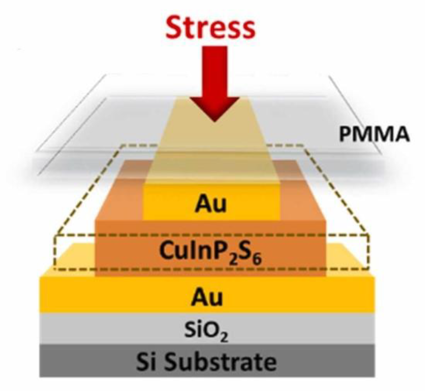
  63. Io, W.F.; Wong, M.-C.; Pang, S.-Y.; Zhao, Y.; Ding, R.; Guo, F.; Hao, J. Strong piezoelectric response in layered CuInP2S6 nanosheets for piezoelectric nanogenerators. Nano Energy 2022, 99, 107371. [Google Scholar] [CrossRef]
  64. Blonsky, M.N.; Zhuang, H.L.; Singh, A.K.; Hennig, R.G. Ab Initio Prediction of Piezoelectricity in Two-Dimensional Materials. ACS Nano 2015, 9, 9885. [Google Scholar] [CrossRef] [PubMed]
  65. Dong, L.; Lou, J.; Shenoy, V.B. Large In-Plane and Vertical Piezoelectricity in Janus Transition Metal Dichalchogenides. ACS Nano 2017, 11, 8242. [Google Scholar] [CrossRef] [PubMed]
  66. Duerloo, K.-A.N.; Ong, M.T.; Reed, E.J. Intrinsic Piezoelectricity in Two-Dimensional Materials. J. Phys. Chem. Lett. 2012, 3, 2871–2876. [Google Scholar] [CrossRef]
  67. Feng, W.; Guo, G.-Y.; Yao, Y. Tunable magneto-optical effects in hole-doped group-IIIA metal-monochalcogenide monolayers. 2D Mater. 2016, 4, 015017. [Google Scholar] [CrossRef]
  68. Fei, R.; Li, W.; Li, J.; Yang, L. Giant piezoelectricity of monolayer group IV monochalcogenides: SnSe, SnS, GeSe, and GeS. Appl. Phys. Lett. 2015, 107, 173104. [Google Scholar] [CrossRef]
  69. Yin, H.; Gao, J.; Zheng, G.-P.; Wang, Y.; Ma, Y. Giant Piezoelectric Effects in Monolayer Group-V Binary Compounds with Honeycomb Phases: A First-Principles Prediction. J. Phys. Chem. C 2017, 121, 25576–25584. [Google Scholar] [CrossRef]
  70. Zhuang, X.; He, B.; Javvaji, B.; Park, H.S. Intrinsic bending flexoelectric constants in two-dimensional materials. Phys. Rev. B 2019, 99, 054105. [Google Scholar] [CrossRef]
  71. Wu, W.; Wang, L.; Li, Y.; Zhang, F.; Lin, L.; Niu, S.; Chenet, D.; Zhang, X.; Hao, Y.; Heinz, T.F.; et al. Piezoelectricity of single-atomic-layer MoS2 for energy conversion and piezotronics. Nature 2014, 514, 470–474. [Google Scholar] [CrossRef]
  72. Lee, J.-H.; Park, J.Y.; Cho, E.B.; Kim, T.Y.; Han, S.A.; Liu, Y.; Kim, S.K.; Roh, C.J.; Yoon, H.-J.; Ryu, H.; et al. Reliable Piezoelectricity in Bilayer WSe2 for Piezoelectric Nanogenerators. Adv. Mater. 2017, 29, 1606667. [Google Scholar] [CrossRef] [PubMed]
  73. Zhao, M.-H.; Wang, Z.-L.; Mao, S.X. Piezoelectric Characterization of Individual Zinc Oxide Nanobelt Probed by Piezoresponse Force Microscope. Nano Lett. 2004, 4, 587–590. [Google Scholar] [CrossRef]
  74. Wang, L.; Liu, S.; Gao, G.; Pang, Y.; Yin, X.; Feng, X.; Zhu, L.; Bai, Y.; Chen, L.; Xiao, T.; et al. Ultrathin Piezotronic Transistors with 2 nm Channel Lengths. ACS Nano 2018, 12, 4903–4908. [Google Scholar] [CrossRef] [PubMed]
  75. Wang, L.; Liu, S.; Zhang, Z.; Feng, X.; Zhu, L.; Guo, H.; Ding, W.; Chen, L.; Qin, Y.; Wang, Z.L. 2D piezotronics in atomically thin zinc oxide sheets: Interfacing gating and channel width gating. Nano Energy 2019, 60, 724–733. [Google Scholar] [CrossRef]
  76. Ghasemian, M.B.; Zavabeti, A.; Abbasi, R.; Kumar, P.V.; Syed, N.; Yao, Y.; Tang, J.; Wang, Y.; Elbourne, A.; Han, J.; et al. Ultra-thin lead oxide piezoelectric layers for reduced environmental contamination using a liquid metal-based process. J. Mater. Chem. A 2020, 8, 19434–19443. [Google Scholar] [CrossRef]
  77. Li, J.; Zhao, T.; He, C.; Zhang, K.-W. Surface oxidation: An effective way to induce piezoelectricity in 2D black phosphorus. J. Phys. D Appl. Phys. 2018, 51, 12LT01. [Google Scholar] [CrossRef]
  78. Wang, X.; He, X.; Zhu, H.; Sun, L.; Fu, W.; Wang, X.; Hoong, L.C.; Wang, H.; Zeng, Q.; Zhao, W.; et al. Subatomic deformation driven by vertical piezoelectricity from CdS ultrathin films. Sci. Adv. 2016, 2, e1600209. [Google Scholar] [CrossRef] [Green Version]
  79. Cao, V.A.; Kim, M.; Hu, W.; Lee, S.; Youn, S.; Chang, J.; Chang, H.S.; Nah, J. Enhanced Piezoelectric Output Performance of the SnS2/SnS Heterostructure Thin-Film Piezoelectric Nanogenerator Realized by Atomic Layer Deposition. ACS Nano 2021, 15, 10428–10436. [Google Scholar] [CrossRef]
  80. Wang, Y.; Vu, L.-M.; Lu, T.; Xu, C.; Liu, Y.; Ou, J.Z.; Li, Y. Piezoelectric Responses of Mechanically Exfoliated Two-Dimensional SnS2 Nanosheets. ACS Appl. Mater. Interfaces 2020, 12, 51662–51668. [Google Scholar] [CrossRef]
  81. Yang, P.-K.; Chou, S.-A.; Hsu, C.-H.; Mathew, R.J.; Chiang, K.-H.; Yang, J.-Y.; Chen, Y.-T. Tin disulfide piezoelectric nanogenerators for biomechanical energy harvesting and intelligent human-robot interface applications. Nano Energy 2020, 75, 104879. [Google Scholar] [CrossRef]
  82. Xue, F.; Zhang, J.; Hu, W.; Hsu, W.-T.; Han, A.; Leung, S.-F.; Huang, J.-K.; Wan, Y.; Liu, S.; Zhang, J.; et al. Multidirection Piezoelectricity in Mono- and Multilayered Hexagonal α-In2Se3. ACS Nano 2018, 12, 4976–4983. [Google Scholar] [CrossRef] [PubMed]
  83. Song, G.; Li, D.; Zhou, H.; Zhang, C.; Li, Z.; Li, G.; Zhang, B.; Huang, X.; Gao, B. Intrinsic room-temperature ferromagnetic semiconductor InCrTe3 monolayers with large magnetic anisotropy and large piezoelectricity. Appl. Phys. Lett. 2021, 118, 123102. [Google Scholar] [CrossRef]
  84. Dimple, D.; Jena, N.; Rawat, A.; Ahammed, R.; Mohanta, M.K.; De Sarkar, A. Emergence of high piezoelectricity along with robust electron mobility in Janus structures in semiconducting Group IVB dichalcogenide monolayers. J. Mater. Chem. A 2018, 6, 24885–24898. [Google Scholar] [CrossRef]
  85. Xiao, W.-Z.; Luo, H.-J.; Xu, L. Elasticity, piezoelectricity, and mobility in two-dimensional BiTeI from a first-principles study. J. Phys. D Appl. Phys. 2020, 53, 245301. [Google Scholar] [CrossRef]
  86. Tan, J.; Wang, Y.; Wang, Z.; He, X.; Liu, Y.; Wang, B.; Katsnelson, M.I.; Yuan, S. Large out-of-plane piezoelectricity of oxygen functionalized MXenes for ultrathin piezoelectric cantilevers and diaphragms. Nano Energy 2019, 65, 104058. [Google Scholar] [CrossRef]
  87. Liu, S.; Chen, W.; Liu, C.; Wang, B.; Yin, H. Coexistence of large out-of-plane and in-plane piezoelectricity in 2D monolayer Li-based ternary chalcogenides LiMX2. Results Phys. 2021, 26, 104398. [Google Scholar] [CrossRef]
  88. Lv, Q.; Qiu, J.; Wen, Q.; Li, D.; Zhou, Y.; Lu, G. Large in-plane and out-of-plane piezoelectricity in 2D γ-LiMX2 (M=Al, Ga and In; X=S, Se and Te) monolayers. Mater. Sci. Semicond. Process. 2023, 154, 107222. [Google Scholar] [CrossRef]
  89. Li, Y.-Q.; Zhang, H.-N.; Yang, C.; Wang, X.-Y.; Zhu, S.-Y.; Wang, X.-C. Ferroelastic Zr2P2XY (X/Y = I, Br, Cl or F; X ≠ Y) monolayers with tunable in-plane electronic anisotropy and remarkable out-of-plane piezoelectricity. Appl. Surf. Sci. 2023, 608. [Google Scholar] [CrossRef]
  90. Qi, Y.; McAlpine, M.C. Nanotechnology-enabled flexible and biocompatible energy harvesting. Energy Environ. Sci. 2010, 3, 1275–1285. [Google Scholar] [CrossRef]
  91. Park, K.-I.; Xu, S.; Liu, Y.; Hwang, G.-T.; Kang, S.-J.L.; Wang, Z.L.; Lee, K.J. Piezoelectric BaTiO3 Thin Film Nanogenerator on Plastic Substrates. Nano Lett. 2010, 10, 4939–4943. [Google Scholar] [CrossRef] [Green Version]
  92. Fu, Y.; Luo, J.; Nguyen, N.; Walton, A.; Flewitt, A.; Zu, X.; Li, Y.; McHale, G.; Matthews, A.; Iborra, E.; et al. Advances in piezoelectric thin films for acoustic biosensors, acoustofluidics and lab-on-chip applications. Prog. Mater. Sci. 2017, 89, 31–91. [Google Scholar] [CrossRef] [Green Version]
  93. Wan, C.; Bowen, C.R. Multiscale-structuring of polyvinylidene fluoride for energy harvesting: The impact of molecular-, micro- and macro-structure. J. Mater. Chem. A 2017, 5, 3091–3128. [Google Scholar] [CrossRef] [Green Version]
  94. Zhu, G.; Wang, A.C.; Liu, Y.; Zhou, Y.; Wang, Z.L. Functional Electrical Stimulation by Nanogenerator with 58 V Output Voltage. Nano Lett. 2012, 12, 3086–3090. [Google Scholar] [CrossRef] [PubMed] [Green Version]
  95. Tang, G.; Yang, B.; Liu, J.-Q.; Xu, B.; Zhu, H.-Y.; Yang, C.-S. Development of high performance piezoelectric d33 mode MEMS vibration energy harvester based on PMN-PT single crystal thick film. Sens. Actuators A Phys. 2014, 205, 150–155. [Google Scholar] [CrossRef]
  96. Li, F.; Lin, D.; Chen, Z.; Cheng, Z.; Wang, J.; Li, C.; Xu, Z.; Huang, Q.; Liao, X.; Chen, L.-Q.; et al. Ultrahigh piezoelectricity in ferroelectric ceramics by design. Nat. Mater. 2018, 17, 349–354. [Google Scholar] [CrossRef]
  97. Hwang, G.-T.; Annapureddy, V.; Han, J.H.; Joe, D.J.; Baek, C.; Park, D.Y.; Kim, D.H.; Park, J.H.; Jeong, C.K.; Park, K.-I.; et al. Self-Powered Wireless Sensor Node Enabled by an Aerosol-Deposited PZT Flexible Energy Harvester. Adv. Energy Mater. 2016, 6, 1600237. [Google Scholar] [CrossRef]
  98. Stoppel, F.; Schröder, C.; Senger, F.; Wagner, B.; Benecke, W. AlN-based piezoelectric micropower generator for low ambient vibration energy harvesting. Procedia Eng. 2011, 25, 721–724. [Google Scholar] [CrossRef]
  99. Doll, J.C.; Petzold, B.C.; Ninan, B.; Mullapudi, R.; Pruitt, B.L. Aluminum nitride on titanium for CMOS compatible piezoelectric transducers. J. Micromech. Microeng. 2010, 20, 25008. [Google Scholar] [CrossRef] [Green Version]
  100. Persano, L.; Dagdeviren, C.; Su, Y.; Zhang, Y.; Girardo, S.; Pisignano, D.; Huang, Y.; Rogers, J.A. High performance piezoelectric devices based on aligned arrays of nanofibers of poly(vinylidenefluoride-co-trifluoroethylene). Nat. Commun. 2013, 4, 1633. [Google Scholar] [CrossRef] [Green Version]
  101. Nan, Y.; Tan, D.; Zhao, J.; Willatzen, M.; Wang, Z.L. Shape- and size dependent piezoelectric properties of monolayer hexagonal boron nitride nanosheets. Nanoscale Adv. 2020, 2, 470–477. [Google Scholar] [CrossRef] [Green Version]
  102. Ma, W.; Lu, J.; Wan, B.; Peng, D.; Xu, Q.; Hu, G.; Peng, Y.; Pan, C.; Wang, Z.L. Piezoelectricity in Multilayer Black Phosphorus for Piezotronics and Nanogenerators. Adv. Mater. 2020, 32, e1905795. [Google Scholar] [CrossRef]
  103. Ding, Z.-K.; Zeng, Y.-J.; Pan, H.; Luo, N.; Zeng, J.; Tang, L.-M.; Chen, K.-Q. Edge states of topological acoustic phonons in graphene zigzag nanoribbons. Phys. Rev. B 2022, 106, L121401. [Google Scholar] [CrossRef]
  104. Zeng, Y.-J.; Feng, Y.-X.; Tang, L.-M.; Chen, K.-Q. Effect of out-of-plane strain on the phonon structures and anharmonicity of twisted multilayer graphene. Appl. Phys. Lett. 2021, 118, 183103. [Google Scholar] [CrossRef]
  105. Zeng, B.; Ding, Z.-K.; Pan, H.; Luo, N.; Zeng, J.; Tang, L.-M.; Chen, K.-Q. Strong strain-dependent phonon hydrodynamic window in bilayer graphene. Appl. Phys. Lett. 2022, 121, 252202. [Google Scholar] [CrossRef]
  106. Chandratre, S.; Sharma, P. Coaxing graphene to be piezoelectric. Appl. Phys. Lett. 2012, 100, 023114. [Google Scholar] [CrossRef] [Green Version]
  107. Ong, M.T.; Duerloo, K.-A.N.; Reed, E.J. The Effect of Hydrogen and Fluorine Coadsorption on the Piezoelectric Properties of Graphene. J. Phys. Chem. C 2013, 117, 3615–3620. [Google Scholar] [CrossRef] [Green Version]
  108. Ganatra, R.; Zhang, Q. Few-Layer MoS2: A Promising Layered Semiconductor. ACS Nano 2014, 8, 4074–4099. [Google Scholar] [CrossRef]
  109. Chhowalla, M.; Shin, H.S.; Eda, G.; Li, L.-J.; Loh, K.P.; Zhang, H. The chemistry of two-dimensional layered transition metal dichalcogenide nanosheets. Nat. Chem. 2013, 5, 263–275. [Google Scholar] [CrossRef]
  110. Tang, D.; Dan, M.; Zhang, Y. High performance piezotronic thermoelectric devices based on zigzag MoS2 nanoribbon. Nano Energy 2022, 104, 107888. [Google Scholar] [CrossRef]
  111. Michel, K.H.; Verberck, B. Theory of elastic and piezoelectric effects in two-dimensional hexagonal boron nitride. Phys. Rev. B 2009, 80, 224301. [Google Scholar] [CrossRef]
  112. Wang, D.; Chen, L.; Wang, X.; Cui, G.; Zhang, P. The effect of substrate and external strain on electronic structures of stanene film. Phys. Chem. Chem. Phys. 2015, 17, 26979–26987. [Google Scholar] [CrossRef] [PubMed]
  113. Qiao, J.; Kong, X.; Hu, Z.-X.; Yang, F.; Ji, W. High-mobility transport anisotropy and linear dichroism in few-layer black phosphorus. Nat. Commun. 2014, 5, 4475. [Google Scholar] [CrossRef] [PubMed] [Green Version]
  114. Ng, L.-R.; Chen, G.-F.; Lin, S.-H. Generating large out-of-plane piezoelectric properties of atomically thin MoS2via defect engineering. Phys. Chem. Chem. Phys. 2021, 23, 23945–23952. [Google Scholar] [CrossRef] [PubMed]
  115. Brennan, C.J.; Koul, K.; Lu, N.; Yu, E.T. Out-of-plane electromechanical coupling in transition metal dichalcogenides. Appl. Phys. Lett. 2020, 116, 053101. [Google Scholar] [CrossRef]
  116. Cui, C.; Hu, W.-J.; Yan, X.; Addiego, C.; Gao, W.; Wang, Y.; Wang, Z.; Li, L.; Cheng, Y.; Li, P.; et al. Intercorrelated In-Plane and Out-of-Plane Ferroelectricity in Ultrathin Two-Dimensional Layered Semiconductor In2Se3. Nano Lett. 2018, 18, 1253–1258. [Google Scholar] [CrossRef] [Green Version]
  117. Esfahani, E.N.; Li, T.; Huang, B.; Xu, X.; Li, J. Piezoelectricity of atomically thin WSe2 via laterally excited scanning probe microscopy. Nano Energy 2018, 52, 117–122. [Google Scholar] [CrossRef] [Green Version]
  118. Kang, S.; Jeon, S.; Kim, S.; Seol, D.; Yang, H.; Lee, J.; Kim, Y. Tunable Out-of-Plane Piezoelectricity in Thin-Layered MoTe2 by Surface Corrugation-Mediated Flexoelectricity. ACS Appl. Mater. Interfaces 2018, 10, 27424. [Google Scholar] [CrossRef]
  119. Kang, S.; Kim, S.; Jeon, S.; Jang, W.-S.; Seol, D.; Kim, Y.-M.; Lee, J.; Yang, H.; Kim, Y. Atomic-scale symmetry breaking for out-of-plane piezoelectricity in two-dimensional transition metal dichalcogenides. Nano Energy 2019, 58, 57. [Google Scholar] [CrossRef]
  120. Seol, D.; Kim, S.; Jang, W.-S.; Jin, Y.; Kang, S.; Kim, S.; Won, D.; Lee, C.; Kim, Y.-M.; Lee, J.; et al. Selective patterning of out-of-plane piezoelectricity in MoTe2 via focused ion beam. Nano Energy 2021, 79, 105451. [Google Scholar] [CrossRef]
  121. Guo, S.-D.; Zhu, Y.-T.; Qin, K.; Ang, Y.-S. Large out-of-plane piezoelectric response in ferromagnetic monolayer NiClI. Appl. Phys. Lett. 2022, 120, 232403. [Google Scholar] [CrossRef]
  122. Cai, H.; Guo, Y.; Gao, H.; Guo, W. Tribo-piezoelectricity in Janus transition metal dichalcogenide bilayers: A first-principles study. Nano Energy 2019, 56, 33–39. [Google Scholar] [CrossRef]
  123. Zhao, Y.-Z.; Jia, H.-J.; Zhao, S.-N.; Wang, Y.-B.; Li, H.-Y.; Zhao, Z.-L.; Wu, Y.-X.; Wang, X.-C. Janus structure derivatives SnP–InS, GeP-GaS and SiP–AlS monolayers with in-plane and out-of-plane piezoelectric performance. Phys. E Low-Dimens. Syst. Nanostruct. 2019, 117, 113817. [Google Scholar] [CrossRef]
  124. Hu, Y.; Li, T.; Liu, L.; Tan, Y.; Hu, L.; Wu, K.; Yang, C. Janus XM-GaS (M=Si, Ge, Sn; X=N, P) monolayers: Multifunctional properties for photocatalysis, piezoelectricity and second harmonic generation. Phys. B Condens. Matter 2020, 594, 412366. [Google Scholar] [CrossRef]
  125. Qiu, J.; Zhang, F.; Li, H.; Chen, X.; Zhu, B.; Guo, H.; Ding, Z.; Bao, J.; Yu, J. Giant Piezoelectricity of Janus M₂SeX (M = Ge, Sn; X = S, Te) Monolayers. IEEE Electron Device Lett. 2021, 42, 561–564. [Google Scholar] [CrossRef]
  126. Wu, Y.; Yang, C.-H.; Zhang, H.-N.; Zhu, L.-H.; Wang, X.-Y.; Li, Y.-Q.; Zhu, S.-Y.; Wang, X.-C. The flexible Janus X2PAs (X = Si, Ge and Sn) monolayers with in-plane and out-of-plane piezoelectricity. Appl. Surf. Sci. 2022, 589, 152999. [Google Scholar] [CrossRef]
  127. Guo, S.-D.; Mu, W.-Q.; Xiao, X.-B.; Liu, B.-G. Intrinsic room-temperature piezoelectric quantum anomalous hall insulator in Janus monolayer Fe2IX (X = Cl and Br). Nanoscale 2021, 13, 12956–12965. [Google Scholar] [CrossRef]
  128. Song, G.; Zhang, C.; Zhang, Z.; Li, G.; Li, Z.; Du, J.; Zhang, B.; Huang, X.; Gao, B. Coexistence of intrinsic room-temperature ferromagnetism and piezoelectricity in monolayer BiCrX3 (X = S, Se, and Te). Phys. Chem. Chem. Phys. 2022, 24, 1091–1098. [Google Scholar] [CrossRef]
Figure 1. The relationship between piezoelectric materials, pyroelectric materials and ferroelectric materials. Piezoelectric materials are classified according to three different criteria.
Materials 16 03107 g001
Figure 2. The schematic diagram of the piezoelectric energy conversion and collection devices (direct piezoelectric effect) and piezoelectric actuators (inverse piezoelectric effect). (a) 33 mode; (b) 11 mode; (c) 31 mode of direct piezoelectric effect. (d) Inverse piezoelectric effect.
Materials 16 03107 g002
Figure 3. The schematic diagram of the ultrathin in-plane films [42,68,101,102]. (a) transition metal dichalcogenides (TMDs) (M = transition metal atoms; X = dichalcogenide atoms). Reproduced with permission from [42]. Copyright 2020, Springer Nature. (b) Top view of D 3 h symmetry materials. Reprinted from [68], with the permission of AIP Publishing. (c) Side view of D 3 h symmetry materials. Reprinted from [68], with the permission of AIP Publishing. (d) Top view of C 2 v symmetry materials. Reprinted from [68], with the permission of AIP Publishing. (e) Side view of C 2 v symmetry materials. Reprinted from [68], with the permission of AIP Publishing. (f) Top view of hexagonal boron nitride (h-BN). Reprinted with permission from [101]. Copyright 2018 Royal Society of Chemistry. (g) Side view of h-BN. Reprinted with permission from [101]. Copyright 2018 Royal Society of Chemistry. (h) Crystalline views of black phosphorene. The P atoms in different positions are marked with different colors. Used with permission of John Wiley & Sons—Books, from [102]. Copyright 2020 WILEY—V C H VERLAG GMBH & CO. KGAA.
Materials 16 03107 g003
Figure 4. Hydrogen and fluorine adsorbed on the different side of graphene induced both in-plane and out-of-plane piezoelectric effects [107]. Reprinted with permission from [107]. Copyright 2013 American Chemical Society.
Materials 16 03107 g004
Figure 5. (a) The schematic diagram of a device for measuring the in-plane piezoelectric stress. Two hydrogen silsesquioxane (HSQ) columns are under the MoS2 film, which are on a SiO2/Si substrate with an Au electrode on the upper side. The AFM probe changes the fold degree of the film and deflects the laser beam, so that the stress can be obtained through the load change on the cantilever beam [33]. Reproduced with permission from [33]. Copyright 2014, Springer Nature. (b) The measured piezoelectric response of MoS2 is odd–even dependent as the number of layers increases [33]. Reproduced with permission from [33]. Copyright 2014, Springer Nature.
Materials 16 03107 g005
Figure 6. (a) Flexible electronic devices based on single layer MoS2 thin films [71]. Reproduced with permission from [71]. Copyright 2014, Springer Nature. (b) The operating principle of this flexible electronic device. When it is stretched and compressed, piezoelectric polarized charges of opposite sign are induced, making it possible to detect piezoelectric output in the external circuit [71]. Reproduced with permission from [71]. Copyright 2014, Springer Nature.
Materials 16 03107 g006
Figure 7. (a) Stacking structure for bilayer-WSe2 [72]. Signs i–v correspond to AA, AB, AA’, AB’ and A’B stacking. Used with permission of John Wiley & Sons—Books, from [72]. Copyright 2017 WILEY—V C H VERLAG GMBH & CO. KGAA. (b) Simulated piezoelectric coefficient (d11) of monolayer WSe2 and stacked WSe2 [72]. Used with permission of John Wiley & Sons—Books, from [72]. Copyright 2017 WILEY—V C H VERLAG GMBH & CO. KGAA. (c) DFT calculation results based on different stacking of WSe2 [72]. Used with permission of John Wiley & Sons—Books, from [72]. Copyright 2017 WILEY—V C H VERLAG GMBH & CO. KGAA.
Materials 16 03107 g007
Figure 8. (a,b) show the atomic structures of armchair and zigzag edges of a hexagonal shaped boron nitride nanosheets structure, respectively [101]. Reprinted with permission from [101]. Copyright 2018 Royal Society of Chemistry. (c,d) show the polarization changes of hexagonal shape boron nitride nanosheets structures along the x- and y-directions, respectively, as a result of stretching [101]. Reprinted with permission from [101]. Copyright 2018 Royal Society of Chemistry.
Materials 16 03107 g008
Figure 9. (a) The atomic structure of rectangular shaped boron nitride nanosheets. The amplified area shows armchair and zigzag boundaries along the x and y directions, respectively [101]. Reprinted with permission from [101]. Copyright 2018 Royal Society of Chemistry. (b) The polarization changes of different size boron nitride nanosheets when strained along the armchair direction and (c) zigzag direction [101]. Reprinted with permission from [101]. Copyright 2018 Royal Society of Chemistry.
Materials 16 03107 g009
Figure 10. (a) Schematics of the experimental setup. The thicknesses of CeO2–x (CGO) films are in the range of ~1.25 to ~1.8 mm [26]. From [26]. Reprinted with permission from AAAS. (b) The phase transition of CGO from cubic to tetragonal phase under an EDC [26]. From [26]. Reprinted with permission from AAAS.
Materials 16 03107 g010
Figure 11. (a,b) The piezoelectric coefficients of some common two-dimensional (2D) materials [54]. Reproduced with permission from [54]. Copyright 2018, Springer Nature.
Materials 16 03107 g011
Figure 12. (a) The different degrees of corrugation engineering [118]. Reprinted with permission from [118]. Copyright 2018 American Chemical Society. (b) The deformation of MoTe2 film driven by Au fold was observed by atomic force microscopy (AFM). Waveform diagram of band excitation (BE) with Vac. The relationship between the amplitude of piezoelectric response force microscope (PFM) and the magnitude of alternating current (AC) voltage [118]. Reprinted with permission from [118]. Copyright 2018 American Chemical Society.
Materials 16 03107 g012
Figure 13. The schematic diagram of the ultrathin out-of-plane films [121,122,123]. (a) Top view of MoSSe. Reprinted from [122], copyright 2019, with permission from Elsevier. (b) Top view of NiClI. Reprinted from [121], with the permission of AIP Publishing. (c) Side view of NiClI. Reprinted from [121], with the permission of AIP Publishing. (d) Top view of the GeP–GaS monolayer. Reprinted from [123], copyright 2020, with permission from Elsevier. (e) Side view of the GeP–GaS monolayer. Reprinted from [123], copyright 2020, with permission from Elsevier.
Materials 16 03107 g013
Figure 14. The schematic diagram of the ultrathin out-of-plane films [86,89]. (a) Top and side view of Sc2CO2 MXene. Reprinted from [86], copyright 2019, with permission from Elsevier. (b) A Sc2CO2 MXene piezoelectric cantilever. Reprinted from [86], copyright 2019, with permission from Elsevier. (c) Top view of the Zr2P2BrCl monolayer. Reprinted from [89], copyright 2023, with permission from Elsevier. (d,e) Side view of the Zr2P2BrCl monolayer from x-z plane and z-y plane. Reprinted from [89], copyright 2023, with permission from Elsevier.
Materials 16 03107 g014
Figure 15. (a) Relationship between piezoelectric coefficient d11 and polarizability of LiMX2 monolayer [87]. Reprinted from [87], copyright 2021, with permission from Elsevier. (b) Comparison of the piezoelectric coefficient d 31 of LiMX2 single layer with reported piezoelectric materials [87]. Reprinted from [87], copyright 2021, with permission from Elsevier.
Materials 16 03107 g015
Figure 16. The schematic diagram of piezoelectric device based on CuInP2S6 (CIPS) [63]. Reprinted from [63], copyright 2022, with permission from Elsevier.
Materials 16 03107 g016
Table 1. Piezoelectric coefficient of common piezoelectric materials (pm V−1).
Materials d 11 (pm V−1) d 12 (pm V−1) d 33 (pm V−1) d 31 (pm V−1) Ref
Graphene/SiO2 14 [54,55]
Graphene oxide 0.24[56]
Graphene (K doped) 0.23[57]
Graphene (Li doped) 0.15[57]
Graphene (H doped) 0.11[57]
Graphene (F doped) 0.0018[57]
Graphene (F, Li doped) 0.30[57]
Graphene (H, F doped) 0.03[57]
BaTiO3 8 [58]
PZT 7–15 [59]
PVDF −36 [60]
C3N4 1 [61]
LiNbO3 7.50 [30]
GaPO4 ~8.50 [62]
CuInP2S6 (3.5 nm) 17.40 [63]
CuInP2S6 (82 nm) 83 [63]
2H-CrS26.15 [64]
2H-CrSe28.25 [64]
2H-CrTe213.45 [64]
2H-MoS23.65 [64,65]
2.5–4 [54,66]
3.73 [66,67,68,69]
3.34 [65]
3.73 [65]
1.35 [30]
1.03 [70]
3 [66,71]
2H-MoSe24.55 [64,65]
4.17 [65]
4.72 [65,66]
2H-MoTe27.39 [64,65]
7.00 [65]
9.13 [65,66]
2H-WS22.12 [64,65]
2.02 [65]
2.19 [65,66]
2H-WSe22.64 [64,65]
2.53 [65]
2.79 [65,66]
~3.26 [72]
2H-WTe24.39 [64,65]
4.29 [65]
4.60 [65,66]
2H-NbS23.12 [64]
2H-NbSe23.87 [64]
2H-NbTe24.45 [64]
2H-TaS23.44 [64]
2H-TaSe23.94 [64]
2H-TaTe24.72 [64]
BeO1.39 [64]
MgO6.63 [64]
CaO8.47 [64]
ZnO8.65 14.30–26.70 [64,73]
23.70 [74]
21.50 [75]
CdO21.70 [64]
PbO73.10 29.603.90[64,76]
α -SbAs243.45−63.65 [69]
α -SbP142.44−27.64 [69]
α -SbN118.29−13.20 [69]
α -AsP18.90−4.74 [69]
α -AsN29.14−5.75 [69]
α -PN6.94−2.44 [69]
β -SbAs1.65 −0.03[69]
β -SbP2.26 −0.03[69]
β -SbN5.30 −0.26[69]
β -AsP0.67 0.01[69]
β -AsN4.83 −0.09[69]
β -PN2.77 −0.09[69]
BP2.18 [64]
surface-oxidized BP88.54 [77]
BAs2.19 [64]
BSb3.06 [64]
AlN2.75 [64]
AlP0.09 [64]
AlAs0.38 0.57[42,64]
AlSb0.79 0.35[42,64]
GaN2.00 [64]
GaP1.29 0.31[42,64]
GaAs1.50 0.13[42,64]
GaSb1.42 0.02[42,64]
InN5.50 [64]
InP0.02 0.39[42,64]
InAs0.08 0.25[42,64]
InSb1.15 0.06[42,64]
BN0.61 [64]
h-BN0.60 [47,66,67]
CdS 32.80 [78]
GaS1.72 [37]
2.06 [47,76]
GaSe1.77 [37]
2.30 [47,68,76]
GaTe1.93 [37]
InS1.12 [37]
InSe1.98 [37]
1.46 [47,76]
InTe1.18 [37]
GeS75.43−50.42 [42,68]
A-GeS20.7111.16 [48]
H-GeS−5.655.65 [48]
GeSe212.13−97.17 [42,68,69]
A-GeSe40.6114.96 [48]
H-GeSe−4.884.88 [48]
SnS144.76−22.89~1.85 [42,68,79]
A-SnS91.56−4.02 [48]
H-SnS−5.285.28 [48]
SnSe250.58−80.31 [42,68,69]
A-SnSe74.730.85 [48]
H-SnSe−4.634.63 [48]
SnS2 2.20 [80]
~5 [81]
α -In2Se3 0.34 [82]
0.53 [63]
In2Te310.64 0.40[83]
Ga2SSe5.23 0.07[37,76]
Ga2STe2.46 0.25[37,76]
Ga2SeTe2.32 0.21[37,76]
In2SSe8.47 0.18[37,76]
In2STe1.91 0.25[37,76]
In2SeTe4.73 0.13[37,76]
GaInS28.33 0.38[37,76]
GaInSe23.19 0.46[37,76]
GaInTe22.99 0.32[37,76]
InCrTe36.94 0.52[83]
1H-WSO1.8 [35]
1H-WSeO1.9 [35]
1H-WTeO2.8 [35]
MoSSe3.76 0.100.02[36,54,65,76]
MoSeTe5.30 0.03[65,76]
MoSTe5.04 0.03[65,76]
WSSe2.26 0.01[65,76]
WSeTe3.52 0.01[65,76]
WSTe3.33 0.01[65,76]
ZrSSe 0.01[84]
ZrSeTe −0.19[84]
ZrSTe 0.004[84]
HfSSe 0.05[84]
HfSeTe 0.41[84]
HfSTe 0.18[84]
BiTeI8.49 0.56[85]
Sc2CO2 0.78[86]
Y2CO2 0.40[86]
La2CO2 0.65[86]
LiAlS22.64 0.53[87,88]
γ -LiAlS28.04 1.17[88]
LiAlSe23.57 0.61[87,88]
γ -LiAlSe210.50 1.62[88]
LiAlTe24.58 0.83[87,88]
γ -LiAlTe211.30 0.39[88]
LiGaS25.03 0.47[87,88]
γ -LiGaS212.02 0.05[88]
LiGaSe26.60 0.49[87,88]
γ -LiGaSe214.48 0.31[88]
LiGaTe28.66 0.70[87,88]
γ -LiGaTe217.44 0.84[88]
LiInS21.48 0.38[87,88]
γ -LiInS25.90 0.12[88]
LiInSe22.18 0.29[87,88]
γ -LiInSe27.81 0.28[88]
LiInTe23.13 0.24[87,88]
γ -LiInTe28.93 0.83[88]
Zr2P2IBr 29.950.93[89]
Zr2P2ICl 91.122.65[89]
Zr2P2IF 33.870.43[89]
Zr2P2BrCl 129.713.21[89]
Zr2P2BrF 22.770.09[89]
Zr2P2ClF 51.050.91[89]
Table 2. Piezoelectric coefficient of common piezoelectric materials (pC N−1).
Materials d 11 (pC N−1) d 12 (pC N−1) d 33 (pC N−1) d 31 (pC N−1) Ref
BaTiO3 19178[90]
~190 [90,91]
ZnO 5.90 [90]
12 [92]
12.40 [93]
~5–10 [90,94]
Quartz2.30 [90]
ST-cut Quartz2.30 [92]
PMN-PT ~2000–3000 [90]
PMN-PZT/PT ~1500–2000 [95,96]
PZT ~60–130 [90]
225–590110[41,44,93]
289–380 [92]
117 [92]
~250–700 [97]
AlN 4.50 [92]
6.40 [92]
5 [98,99]
Sapphire 6.40 [92]
GaN 4.50 [92]
128° cut LiNbO3 12 [92]
36° YX cut LiTaO3 12 [92]
PVDF Film −3323[44]
−35 [92]
~20–30 [90,100]
Table 3. Relevant information of the experimentally confirmed piezoelectric 2D materials [54]. Reproduced with permission from [54]. Copyright 2018, Springer Nature.
2D MaterialsCrystal StructurePiezoelectric
Direction
Estimated PiezocoefficientNotes
Monolayer MoS2HexagonalIn-plane
Angle dependence
d 11 = 2.5 4   p m / V [66]
e 11 = 250 400   p C / m [33,66]
Odd–even effect with the thickness increased
Monolayer h-BNHexagonalIn-plane
Angle dependence
e 11 = 100 400   p C / m [66]Odd–even effect with the thickness increased [53]
Graphitic carbon nitride In-plane e 11 = 218   p C / m [61]Existence of piezoelectricity regardless of thickness
Doped grapheneHexagonalOut-of-plane d 33 = 1.4   n m / V [55]Extrinsic piezoelectricity
α -In2Se3RhombohedralOut-of-plane and in-plane Indirectly confirmed by the ferroelectricity [116]
Janus MoSSeHexagonalOut-of-plane and in-plane d 33 = 0.1   p m / V [36]
Disclaimer/Publisher’s Note: The statements, opinions and data contained in all publications are solely those of the individual author(s) and contributor(s) and not of MDPI and/or the editor(s). MDPI and/or the editor(s) disclaim responsibility for any injury to people or property resulting from any ideas, methods, instructions or products referred to in the content.

