Article

Impact of Rh, Ru, and Pd Leads and Contact Topologies on Performance of WSe2 FETs: A First Comparative Ab Initio Study

Department of Electronics and Electrical Engineering and Institute of Electronics, National Yang Ming Chiao Tung University, Hsinchu 300, Taiwan
*
Author to whom correspondence should be addressed.
Materials 2024, 17(11), 2665; https://doi.org/10.3390/ma17112665
Submission received: 4 April 2024 / Revised: 10 May 2024 / Accepted: 23 May 2024 / Published: 1 June 2024
(This article belongs to the Section Materials Simulation and Design)

Abstract

:
2D field-effect transistors (FETs) fabricated with transition metal dichalcogenide (TMD) materials are a potential replacement for the silicon-based CMOS. However, the lack of advancement in p-type contact is also a key factor hindering TMD-based CMOS applications. The less investigated path towards improving electrical characteristics based on contact geometries with low contact resistance (RC) has also been established. Moreover, finding contact metals to reduce the RC is indeed one of the significant challenges in achieving the above goal. Our research provides the first comparative analysis of the three contact configurations for a WSe2 monolayer with different noble metals (Rh, Ru, and Pd) by employing ab initio density functional theory (DFT) and non-equilibrium Green’s function (NEGF) methods. From the perspective of the contact topologies, the RC and minimum subthreshold slope (SSMIN) of all the conventional edge contacts are outperformed by the novel non-van der Waals (vdW) sandwich contacts. These non-vdW sandwich contacts reveal that their RC values are below 50 Ω∙μm, attributed to the narrow Schottky barrier widths (SBWs) and low Schottky barrier heights (SBHs). Not only are the RC values dramatically reduced by such novel contacts, but the SSMIN values are lower than 68 mV/dec. The new proposal offers the lowest RC and SSMIN, irrespective of the contact metals. Further considering the metal leads, the WSe2/Rh FETs based on the non-vdW sandwich contacts show a meager RC value of 33 Ω∙μm and an exceptional SSMIN of 63 mV/dec. The two calculated results present the smallest-ever values reported in our study, indicating that the non-vdW sandwich contacts with Rh leads can attain the best-case scenario. In contrast, the symmetric convex edge contacts with Pd leads cause the worst-case degradation, yielding an RC value of 213 Ω∙μm and an SSMIN value of 95 mV/dec. While all the WSe2/Ru FETs exhibit medium performances, the minimal shift in the transfer curves is interestingly advantageous to the circuit operation. Conclusively, the low-RC performances and the desirable SSMIN values are a combination of the contact geometries and metal leads. This innovation, achieved through noble metal leads in conjunction with the novel contact configurations, paves the way for a TMD-based CMOS with ultra-low RC and rapid switching speeds.

1. Introduction

With continued transistor downscaling, the short channel effect becomes more notorious and urgently needs alleviation [1,2,3,4,5]. In order to address this challenge, the emerging 2D transition metal dichalcogenides (TMDs) are referred to as promising candidates owing to their exceptional properties [6,7,8,9,10,11], such as a desirable band gap, dangling-bond-free surface, slight mobility variation, and ultra-thin thickness [11,12,13,14,15,16,17,18]. Among these TMDs, WSe2 has attracted great interest in p-FETs, with early reports of WSe2-based FETs showing hole mobility [19,20,21,22]. These experimental hole mobilities are reported within 100~500 cm2/V-s. Also, WSe2 has pronounced thermal and environmental stability [23], making it an attractive channel material for TMD-based FETs.
Inevitably, 2D TMD-based FETs have contact interfaces with 3D metal leads [24,25,26,27,28,29,30], serving as source and drain regions. For example, Jacko Rastikian et al. used Co and Pd as contacts to obtain high-performance p-type WSe2 FETs [27]. Dae Hyun Jung et al. reported that Ti/Au were deposited as contacts for their monolayer WSe2 FETs [29]. Ang-Sheng Chou et al. proposed that Sb-Pt contact engineering can achieve the excellent performance of p- and n-type monolayer WSe2 FETs [30]. Fundamentally, contact geometries include top and edge contacts [14,17,31]. Edge-contacted configurations enhance the in-plane carrier injection to the atomically thin TMD and involve no additional tunneling barrier along the current path [14,17]. Thus, such contacts minimize the contact resistance (RC) compared to top contacts. Moreover, edge-contacted configurations provide optimal device scalability [32] and compatible 3D integration [33]. Based on the advantages mentioned above, edge contacts are adopted for this study. Furthermore, the atomic-scale characterization of the interfaces has garnered interest in research over the past years [34,35,36,37], so the atomistic structural variation across the TMD/metal interfaces is also considered. The atomistic interfaces can be divided into two categories based on their structural variants: symmetric convex and concave edge contacts. The contacts mentioned above are shown and further detailed in Figure 1. The symmetric convex edge contacts mean that the convex surface of the source electrode, indicated by the yellow line in Figure 1a, aligns with the TMD across the interface. Conversely, the symmetric concave counterparts shown in Figure 1b are the opposite. Hence, the discrepancy between these edge contacts can be indicated at the atomistic level, demonstrating the different electrical behaviors.
Apart from the above-mentioned edge contacts, a novel contact configuration is also being studied. Conventionally, the top contacts can be easily constructed by deposition, meaning the manufacturing challenges are smaller than the edge counterpart but exhibit a van der Waals (vdW) gap between the leads and TMD. Such a vdW gap inevitably leads to an undesirable tunnel barrier, further degrading the carrier injection efficiency across the interfaces [17,38] for Schottky barrier (SB) TMD-based FETs. That is, alleviating tunnel barriers can initially improve the electrical contacts. Yaochen Sheng et al. have demonstrated that contact behaviors can be improved by removing the facial chalcogen atoms of the TMD to eliminate the tunneling barrier induced by the vdW gap through direct contact with metal leads [39]. As shown in the previous work [39], the source/drain of the TMD can be patterned after lithography and development. Next, the defined TMD is then treated by H2 plasma etching. The upper chalcogen atoms are thus removed after the weakest-ion bombardment. After metal deposition, direct metal contact with the TMD can be formed at the source/drain regions, which are expected to improve the RC. Undoubtedly, these manufacturing techniques and steps are feasible so far, and the above-mentioned process is subsequently generalized in our work to create a novel contact topology. Our primary focus is combining edge and direct top contact, allowing both elements to employ their strengths to obtain optimized contact performances. Thus, partial selenium replacement for both sides of a TMD is critical to achieving novel contact engineering. In the beginning, the edge-contacted interfaces are fabricated in a conventional process. Second, the upper side of the TMD has to be patterned to define source/drain “extension” regions near the TMD/metal interfaces, compared to the symmetric convex edge contacts. Such regions then undergo H2 bombardment, as previously mentioned. Successively, the upper chalcogen atoms near the TMD/metal interfaces are replaced with those of the edge-contacted metal leads by metal deposition. However, the adoption of such contacts is not without any obstacles. The non-vdW contacts have partly been formed so far, and the subsequent difficulties have added layers of complexity to fabrication. Substituting the chalcogen atoms of the bottom layer with Rh, Ru, or Pd adds challenges to the sample fabrication. The hurdles inevitably lie in flipping the semi-finished device upside down, without causing any defects, to continue the successive processing steps. After that, the original bottom layer of the device can be further processed to complete the non-vdW sandwich contacts. Repeating patterning and deposition, as mentioned above, can replace these chalcogen atoms with metal lead counterparts at the remaining source/drain “extension” regions. Due to meticulous “flip” treatments, the relevant processes have remained technically unfeasible and have not yet been experimentally realized. Nevertheless, semiconductor technology is advancing quickly, so the realization of such a novel contact configuration can be expected. As highlighted by two yellow ellipses in Figure 1c, the so-called non-vdW sandwich contacts can be thus proposed through high manufacturing complexity. Although non-vdW sandwich contact engineering requires a highly sophisticated and complex process for existing techniques, our simulated results can shed light on developing such a contact-engineered FET at the initial state.
In addition to these contact geometries, noble metals, as the contact leads, play a crucial role in achieving extraordinary nanomaterial-based FETs [40]. For example, Rh is prone to make near-Ohmic contacts with single-walled carbon nanotube field-effect transistors (CNTFETs) [40]. For scaled edge-contacted CNTFETs, the RC exhibits better scaling behaviors by decreasing the contact length of the Rh leads [41]. For micro-electromechanical systems (MEMSs), Rh emerges as a highly ranked contact metal, considering its high melting point and low RC. Hence, the idea of using Rh is generalized in our study to form WSe2/Rh contacts and is anticipated to improve the electrical characteristics of p-type WSe2 FETs. Additionally, the scientific community has traditionally used Pd as the contact metal [42,43,44,45,46]. The high work function of Pd is 5.2 eV [47], which thus facilitates the noble metal to inject and conduct the holes into the WSe2 channel through the suitable Fermi level (EF) alignment of the metal leads with the edge of the valence band in the TMD. Patoary et al. proposed that model calculations can achieve an approximately ideal SS value and a larger ION of ~270 µA/µm [48]. Therefore, WSe2/Pd contacts are also constructed in conjunction with the various contact topologies and extensively studied in our research. In addition to the contact metals mentioned above, Ru is also an attractive contact metal for next-generation interconnects [49,50,51]. This metal can reduce the resistivity size effect and electromigration [52,53,54,55]. Also, MEMSs have utilized low-resistance Ru to improve contact behaviors [56,57]. These theoretical and experimental results suggest that Ru has a vast potential for excellent electrical contacts. In the TMD-based FET community, O’Brien et al. experimentally reported the low RC of WSe2 FETs with Ru contacts, accompanied by an on-state current (ION) of 50 μA/μm and subthreshold swing (SS) of 141 mV/dec [58]. Due to these intriguing properties, WSe2/Ru contacts have become a rising star and are worth further study. Although the above-published works indicate excellent p-type performances, there is still a puzzle about the emphasis on the quantum transport concerning the RC and contacted configurations. Therefore, it is urgent to establish the optimal combination involving contact metals and their respective configurations.
In this research, our attention is directed toward the novel variants of contact configurations and noble metals. DFT + NEGF calculations are conducted to study the electrical characteristics of WSe2/metal (Rh, Ru, Pd) in the different contact-engineered configurations. Our findings unveil that the Schottky barrier widths (SBWs) and Schottky barrier heights (SBHs) are extremely sensitive to contact geometries and noble metals. The lowest RC and nearly ideal SS value can be achieved by the non-vdW sandwich WSe2/Rh FETs, further providing theoretical support for the design of ultra-scaled TMD-based FETs.

2. Materials and Methods

2.1. DFT Simulations

The structural relaxations for WSe2/metal (Rh, Ru, and Pd) contacts are performed based on density functional theory (DFT) using the exchange-correlation potential of local density approximation (LDA) and projector augmented wave (PAW) pseudopotentials [59], as implemented in Vienna ab initio Simulation Package (VASP) [60,61]. One 16 Å vacuum layer is set along the vertical direction to avoid the spurious interaction between adjacent repeating cells. The cutoff energy of 400 eV is used for the plane wave expansion. A k-point mesh of 1 × 10 × 1 is adopted in the reciprocal lattice. For the WSe2 monolayer contacted to the metal leads, the rectangular surfaces (110) of the metal leads are adopted to fit WSe2 with a sufficiently low interfacial strain below 7%. The transport direction is along the x-direction, while in the y-direction, periodic boundary conditions are employed to represent an infinite WSe2 monolayer and two metal leads. During the structural relaxation, the atomic z-coordinates of the Se atoms away from the WSe2/metal interfaces are fixed. The stopping criterion for the ionic relaxations in these contact structures with different contact geometries is the remnant force on each atom below 0.05 eV/Å, and the convergence criterion for electronic iterations is 10−4 eV.

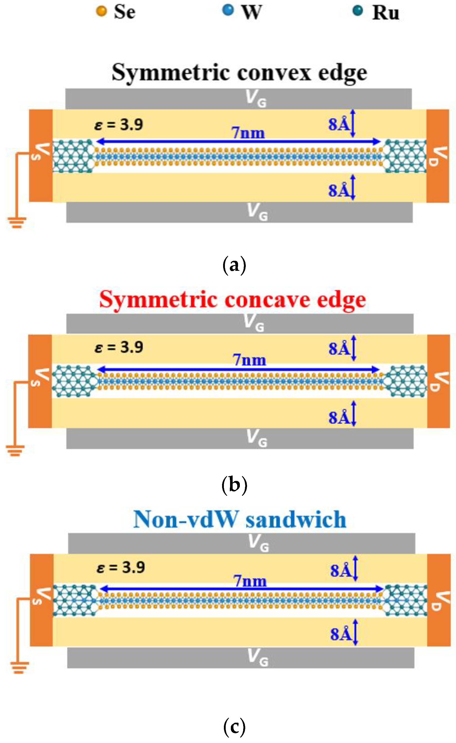
2.2. Device Structures and Transport Simulations

All schematic views of the simulated double-gate device structures are shown in Figure 2 and generated using the NEGF-DFT NanoDCAL package [62,63,64]. NanoDCAL employs the double-zeta-polarized (DZP) atomic orbital basis set to extend all physical quantities. The standard norm-conserving pseudopotential defines the atomic cores [65]. LDA is chosen for the exchange-correlation functional. The truncation energy of the self-consistent atomic orbital is set to 80 Hartree. The convergence criterion of the density and Hamiltonian matrices in the self-consistent calculations is set to 10−4 eV. Spin-orbit coupling (SOC) and the temperature of 300 K are both considered in the theoretical simulations. The channel length (L) equals 7 nm, and the gate length is set to 9.8 nm. The device structure is periodic in the channel width direction. The k-point mesh in the self-consistent calculation is set to 1 × 10 × 1 for the central scattering regions. A 1 × 100 × 1 k-grid is used to calculate the transport current. The equivalent oxide thickness (EOT) is 8 Å, and the dielectric constant is 3.9. The drain-to-source voltage (VDS) is applied at −50 mV [66] to allow the drain current (ID) to be determined by the nature of the SB.

3. Results and Discussion

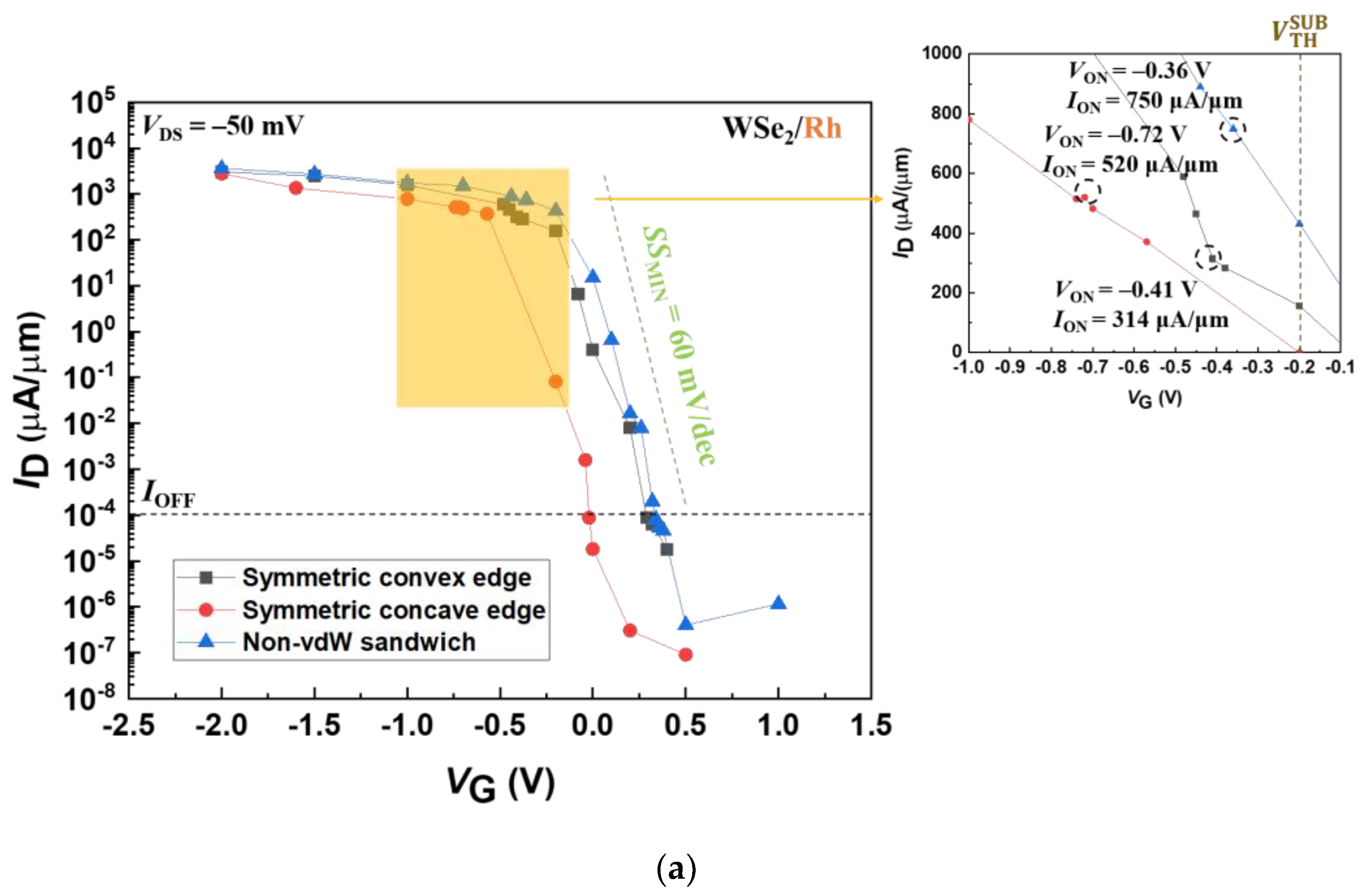
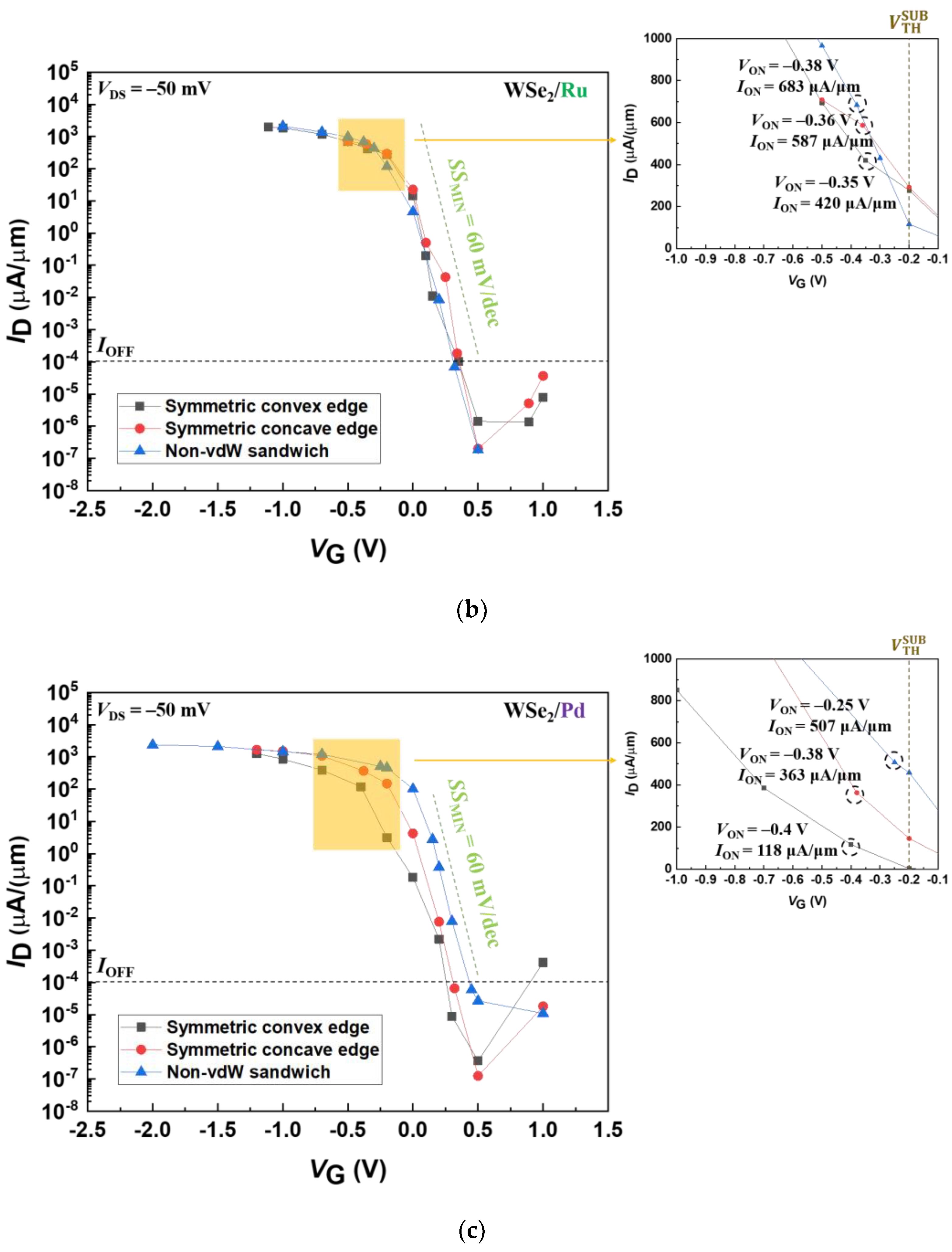
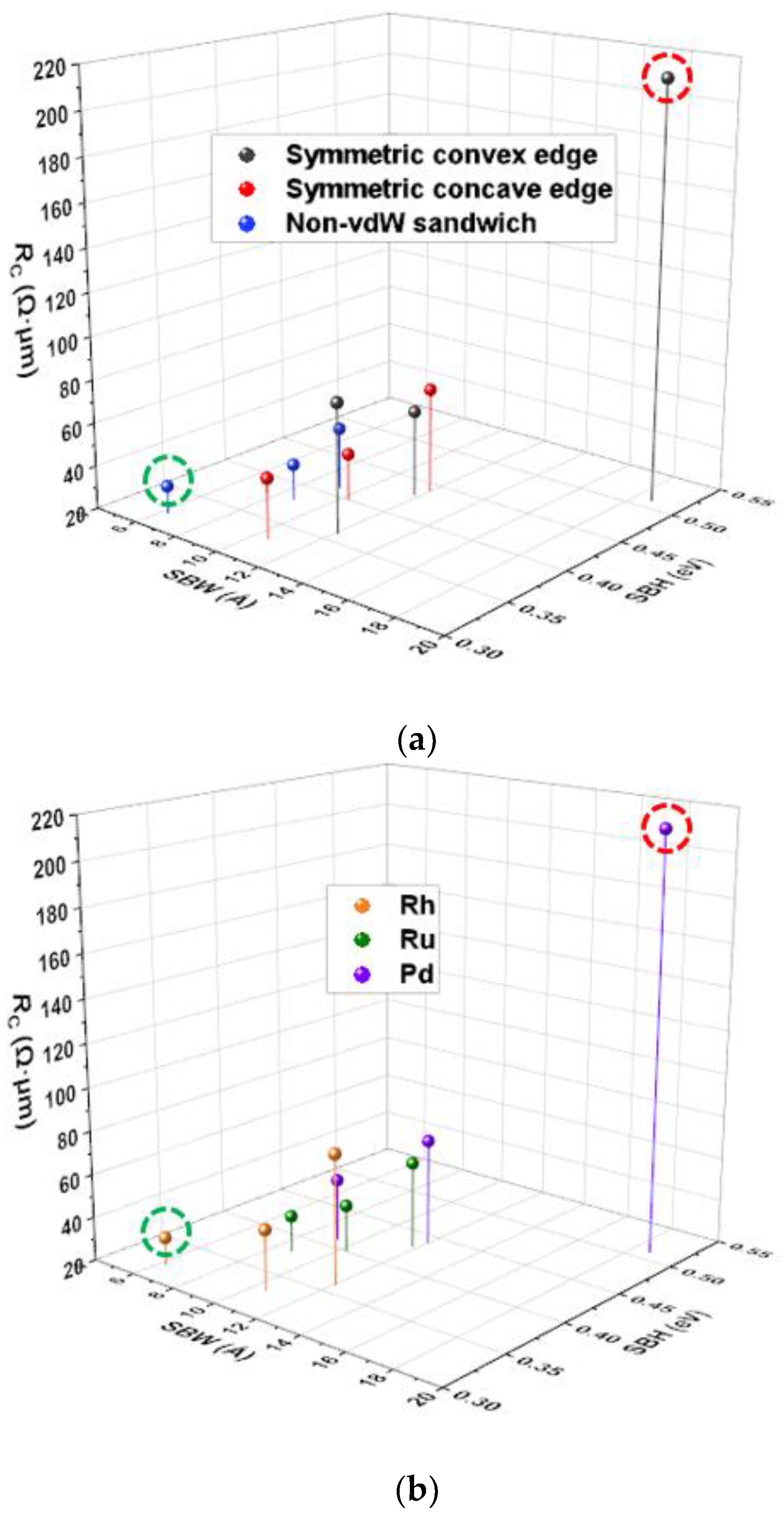
3.1. Transport Properties
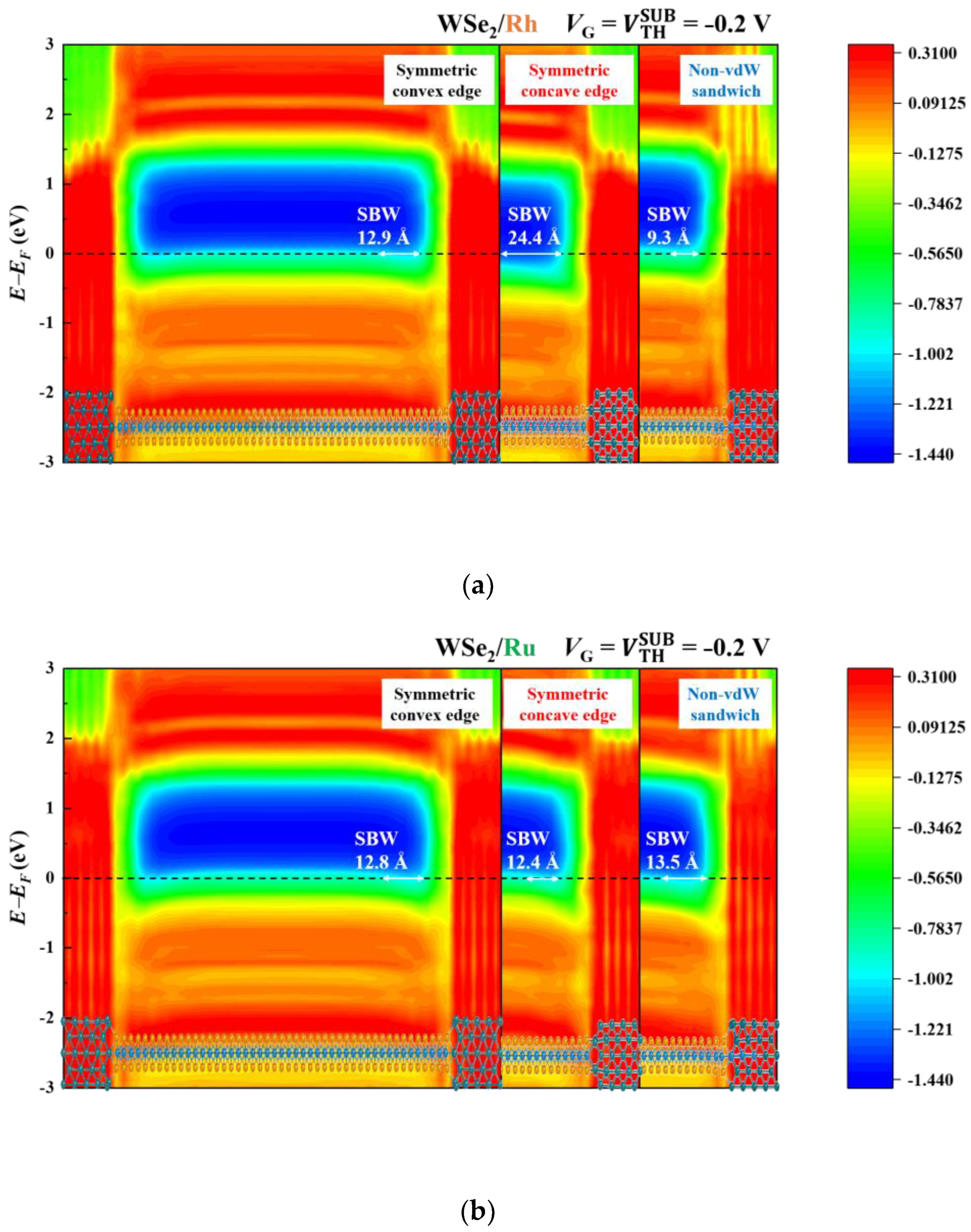
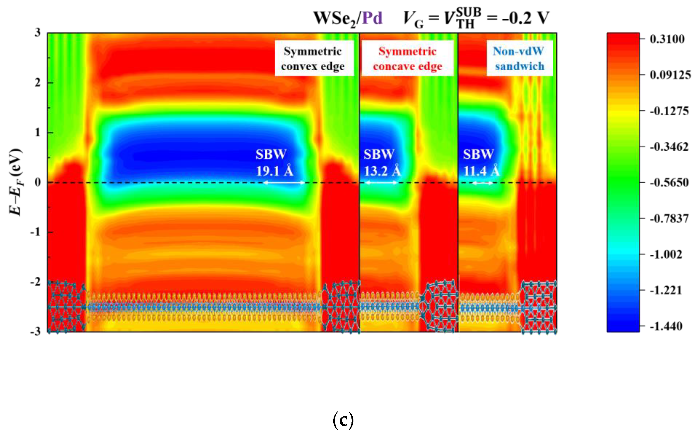
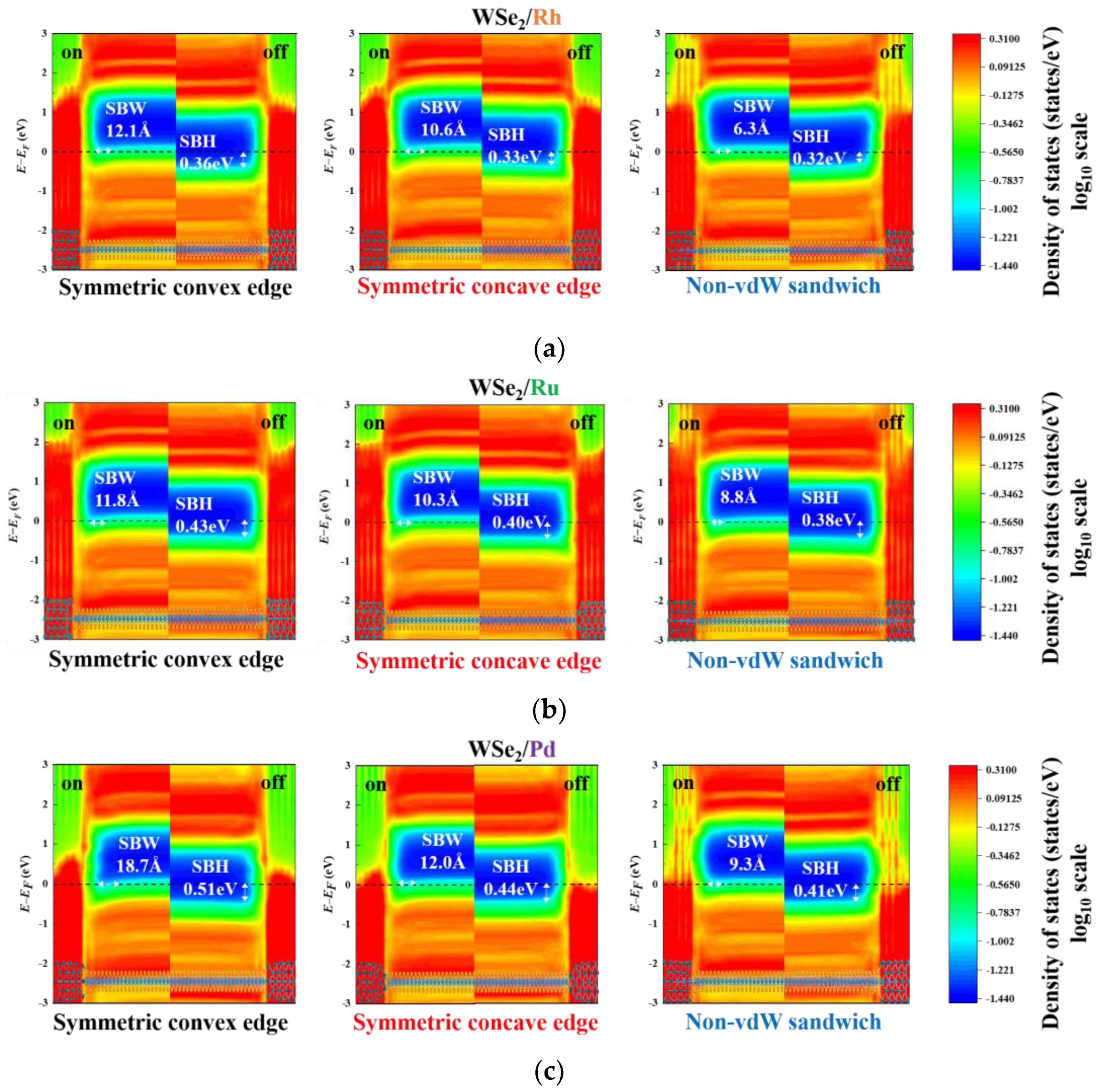
Past work reported by Jung et al. [67] shows that the best sheet resistance (RSH) of WSe2, which has less than ten layers, maintains about 103 Ohm/sq. Given that our simulated 2D FETs do not include electron-phonon scattering and defects, the WSe2 monolayer can be a few Ω∙μm. Hence, such a relatively low RSH makes the RC dominate the resistance of the whole system. To access the RC of these various contact-engineered WSe2/metal FETs, the ION among the various WSe2/metal contact geometries is first determined. Herein, the ION is the ID when the difference between the gate voltage (VG) at the off-state current (IOFF) level and the turn-on voltage (VON) reaches 0.7 V, i.e., |VGVON| = 0.7 V [68]. Also, IOFF is defined as 10−4 μA/μm, represented by the horizontal dashed lines in Figure 3. Additionally, a subthreshold voltage ( V T H S U B ) of −0.2 V is referred to as a representative VG in the subthreshold region and will be discussed in more detail later. Apparently, not only are these on/off current ratios larger than 106, but their corresponding high ION values are within the range of 118 μA/μm to 750 μA/μm in the insets of Figure 3a–c. These notably surpass the previous works, making one confident in further studying these three structural variants.
To look closer at the effects of the different contact configurations on their electrical behaviors, we also consider the minimum subthreshold swing (SSMIN). These computed results, shown in Table 1, are further compared below. Regardless of the contact leads, the non-vdW sandwich contacts have the highest ION levels (507~750 μA/μm), followed by the symmetric concave edge contacts (363~587 μA/μm) and their symmetric convex counterparts (118~420 μA/μm). For the RC, the opposite thus applies to these contact geometries. The lowest RC levels reach as low as 33 to 49 Ω∙μm for the non-vdW sandwich contacts. The second lowest levels increase to 42~69 Ω∙μm for the symmetric concave contacts, followed by the highest levels of 60~213 Ω∙μm for their convex counterparts. The above-calculated results suggest that the non-vdW sandwich contacts are superior to the others. Also, considering the steep switching characteristics, the non-vdW sandwich contacts exhibit the fastest switching rate. Table 1 shows the contacts above with the SSMIN values from 63 to 67 mV/dec. The symmetric concave edge contacts are ranked second fastest, ranging from 67 to 74 mV/dec, followed by their convex counterparts (81~95 mV/dec). Based on these results, non-vdW sandwich contacts achieve optimal device performances in terms of RC and SSMIN.
The contact leads can also affect the performances of TMD-based FETs due to the various SBs across the TMD/metal interfaces [69,70]. Through a deep dive into comparing a contact topology with different contact metals, further analysis can be performed by revisiting Figure 3. First, the WSe2/Rh FETs generate more shifts in the IDVG curves than the WSe2/Pd FETs. The former shows approximately 500 mV and the latter 250 mV. Furthermore, compared with the above two FETs, the contact-engineered WSe2/Ru counterparts exhibit minimal shifts (~50 mV). Via the insets of Figure 3a–c, the shifts of VON clearly show high consistency with those of the transfer characteristics. These VON values shift slightly due to the insubstantial shifts among the corresponding IDVG curves, and vice versa. This suggests that WSe2/Ru FETs can achieve the most stable circuit operation [71], outperforming their WSe2/Rh and WSe2/Pd counterparts.

3.2. Band Diagrams

SBWs and SBHs across the TMD/metal interfaces are well-known as critical factors for dominating the performances of the TMD-based FETs [68]. Such two quantities can be indicated by the band diagrams revealed by the local device density of states (LDDOS), further impacting quantum transport. At room temperature, current transport is mainly limited by an SBW when not overcoming an SBH thoroughly. Such a primary consideration is essential when the FET is not turned on. At this stage, VG = V T H S U B = −0.2 V is taken to be an example. The corresponding LDDOS for these contact-engineered FETs are illustrated in Figure 4. From Figure 4a, the WSe2/Rh FET based on the symmetric concave edge contacts displays the widest SBW of 24.4 Å, compared to the other two contact geometries. This widest SBW suggests that such a WSe2/Rh contact configuration offers the lowest ID. The current flow is lower than the others by four orders of magnitude, as observed in Figure 3a. Next, no significant SBW difference (12.4~13.5 Å) among the three WSe2/Ru contact topologies is shown in Figure 4b, although the non-vdW sandwich contacts form the widest SBW. Thus, no considerably different transfer characteristics are established in Figure 3b. For the WSe2 contacts with the Pd leads, the symmetric convex edge contacts exhibit the widest SBW (19.1 Å) in Figure 4c, accompanied by the lowest ID (a few μA/μm) in Figure 3c. When the applied VG reaches VON, the FET is then turned on. The simulated WSe2 FETs in the on states are displayed in the left panels of each band diagram, as shown in Figure 5. In contrast, the corresponding off states are seen in the right panels. The SBWs and SBHs are depicted on each diagram’s left and right sides. For a single WSe2 FET, a significant difference exists among these contact geometries. Take the WSe2/Ru contacts in Figure 5b as an example. These undesirable SBHs appear over the range of 0.38 to 0.43 eV, and their corresponding SBWs vary from 8.8 Å to 11.8 Å. Direct and thermally assisted tunneling behaviors are involved in carrier transport across an SB at 300 K. In the on state, the non-vdW sandwich WSe2/Ru FET has the narrowest SBW of 8.8 Å and the lowest SBH of 0.38 eV. Consequently, this simulated FET achieves the highest ION of 683 μA/μm due to the minimal SBH and SBW, implying the lowest RC value. Next, the SBW is 10.3 Å for the symmetric concave edge contacts, which is more significant than the above-mentioned counterpart, thus having the second-best ION of 587 μA/μm. Lastly, the ION of 420 μA/μm flows through the symmetric convex edge contacts with the highest SBH of 0.43 eV and the widest SBW of 11.8 Å.
These SB FETs display various electrical properties through all the above contact-engineered geometries. The current can be increased by decreasing the SBW due to the corresponding tunneling probability. Also, the holes with energies above the SBH can be injected into the TMD channel. After conversion to RC from ID at VDS = −50 mV, the above RC values are categorized into contact geometries and contact leads, as shown in Figure 6a,b. From the comparison of these nine WSe2/metal FETs, the change in RC is interestingly consistent with the trend of the contact-engineered SBWs. As depicted in Figure 6a, the non-vdW sandwich contacts (marked in blue) tend to yield a narrower SBW than their symmetric counterparts (marked in red for concave and black for convex, respectively). The data shown in Figure 6b further suggest that Rh (orange) and Ru (green) offer a narrower SBW than Pd (purple). What is even worse is that the higher SBH is formed at various contacted-engineered WSe2/Pd interfaces compared to other corresponding interfaces constructed by Ru and Pd. Thus, the corresponding ION is partly hindered by the SBH, therefore deteriorating the contact performances of these WSe2/Pd contacts. Finally, the best- and worst-case scenarios are obtained considering the combination of the contact geometries and leads. The WSe2/Rh non-vdW sandwich contacts exhibit the lowest SBH of 0.32 eV, whereas their WSe2/Pd symmetric convex counterparts display the most undesirable SBH above 0.5 eV. Therefore, the former is expected to have a negligible SBH by applying VON, and the latter has a non-negligible SBH at VON. Consequently, the WSe2/Rh non-vdW sandwich contacts display the lowest RC of 33 Ω∙μm, whereas their WSe2/Pd symmetric convex edge counterparts show the highest RC of 213 Ω∙μm. Conclusively, our demonstration provides a novel strategy to achieve the lowest RC and SSMIN, unveiling the advantages of noble metals over conventional metals. Combining the effects of noble metals and contact-engineered topologies establishes the optimized electrical performances of WSe2 FETs. Our optimization serves as a reasonable starting point for fabricating such ultra-scaled FETs.

4. Conclusions

The first comparative study presents the electrical performances of the different contact-engineered WSe2 FETs with various noble metal leads. Regardless of the contact metal, the novel non-vdW sandwich contacts improve the ION, RC, and SSMIN to the greatest extent. The symmetric concave edge contacts exhibit middling performances, followed by their symmetric convex counterparts. Additionally, the contact metals have quite an impact on the electrical performances of the WSe2 FETs. The WSe2/Rh FETs are first unveiled, showing the distinguishable RC value of 33 Ω∙μm and the nearly ideal SSMIN of 63 mV/dec for the non-vdW sandwich contacts. When viewed from another angle, although the Rh leads can lead to the lowest RC and SSMIN, the Ru leads offer minor instability in the circuit in terms of the minimal ID-VG shifts. Moreover, such WSe2/Ru FETs exhibit significantly small RC (37 Ω∙μm) and SSMIN (67 mV/dec) values in non-vdW sandwich contacts. These initial results allow us to evaluate the performances of the TMD-based CMOS from a different perspective. Eventually, the WSe2/Pd FETs based on the non-vdW sandwich contacts yield a slightly higher RC (49 Ω∙μm) and lower SSMIN (64 mV/dec) than the WSe2/Ru FETs. However, such WSe2/Pd FETs formed by the symmetric convex contacts cause the degradation of RC and SSMIN, increasing RC and SSMIN up to 213 Ω∙μm and 95 mV/dec. The corresponding performance deterioration in RC is approximately 4.5 times higher, while SSMIN increases by almost 1.5 times. Furthermore, the above-mentioned results enable a more comprehensive look at the TMD-based FETs from an atomistic perspective. In practice, the edge contact interface exhibits a mixture of convex and concave constituents after fabrication. Therefore, the overall electrical performance is affected by these two components. By choosing suitable noble metal leads, the edge-contacted WSe2 FETs have an RC within 42~213 Ω∙μm, accompanied by an SSMIN from 67 to 95 mV/dec. The rapidly advancing technology can finally realize the proposed non-vdW sandwich contacts. This non-vdW novelty theoretically maintains an RC at a low level of 33~49 Ω∙μm, outperforming the edge-contacted configurations. Additionally, the novelty has a faster switching transition. Their SSMIN values range from 63 to 67 mV/dec, superior to the edge-contacted topologies. Our simulations display excellent potential for high-performance p-type FETs, paving the way for a future TMD-based CMOS with a low RC and high switch speed during the off/on transition.

Author Contributions

Conceptualization, C.-H.C. and C.-Y.L.; methodology, C.-H.C.; software, H.-Y.L., S.-E.N., Y.-T.C. and C.-E.T.; validation, C.-H.C., H.-Y.L., S.-E.N., Y.-T.C. and C.-E.T.; formal analysis, C.-H.C.; investigation, C.-H.C.; resources, C.-Y.L.; data curation, C.-H.C., H.-Y.L., S.-E.N., Y.-T.C. and C.-E.T.; writing—original draft preparation, C.-H.C.; writing—review and editing, C.-H.C.; visualization, C.-H.C., H.-Y.L., S.-E.N., Y.-T.C. and C.-E.T.; supervision, C.-Y.L.; project administration, C.-Y.L.; funding acquisition, C.-Y.L. All authors have read and agreed to the published version of the manuscript.

Funding

This work was financially supported by the “Center for the advanced Semiconductor Technology Research” from The Featured Areas Research Center Program within the framework of the Higher Education Sprout Project by the Ministry of Education (MOE) in Taiwan. This work was also supported in part by the National Science and Technology Council, Taiwan, under Grant No. NSTC 113-2119-M-A49-006-MBK.

Institutional Review Board Statement

Not applicable.

Informed Consent Statement

Not applicable.

Data Availability Statement

The data in this study can be provided upon request.

Acknowledgments

We thank National Center for High-performance Computing (NCHC) for providing computational and storage resources.

Conflicts of Interest

The authors declare no conflict of interest.

References

  1. Kwon, D.; Chatterjee, K.; Tan, A.J.; Yadav, A.K.; Zhou, H.; Sachid, A.B.; Dos Reis, R.; Hu, C.; Salahuddin, S. Improved subthreshold swing and short channel effect in FDSOI n-channel negative capacitance field effect transistors. IEEE Electron Device Lett. 2017, 39, 300–303. [Google Scholar] [CrossRef]
  2. Chan, T.; Chen, J.; Ko, P.; Hu, C. The impact of gate-induced drain leakage current on MOSFET scaling. In Proceedings of the 1987 International Electron Devices Meeting, Washington, DC, USA, 6–9 December 1987. [Google Scholar]
  3. Troutman, R.R. VLSI limitations from drain-induced barrier lowering. IEEE J. Solid-State Circuits 1979, 14, 383–391. [Google Scholar] [CrossRef]
  4. Duan, X.; Wang, C.; Pan, A.; Yu, R.; Duan, X. Two-dimensional transition metal dichalcogenides as atomically thin semiconductors: Opportunities and challenges. Chem. Soc. Rev. 2015, 44, 8859–8876. [Google Scholar] [CrossRef] [PubMed]
  5. Taur, Y. CMOS design near the limit of scaling. IBM J. Res. Dev. 2002, 46, 213–222. [Google Scholar] [CrossRef]
  6. Wang, Q.H.; Kalantar-Zadeh, K.; Kis, A.; Coleman, J.N.; Strano, M.S. Electronics and optoelectronics of two-dimensional transition metal dichalcogenides. Nat. Nanotechnol. 2012, 7, 699–712. [Google Scholar] [CrossRef] [PubMed]
  7. Jariwala, D.; Sangwan, V.K.; Lauhon, L.J.; Marks, T.J.; Hersam, M.C. Emerging device applications for semiconducting two-dimensional transition metal dichalcogenides. ACS Nano 2014, 8, 1102–1120. [Google Scholar] [CrossRef] [PubMed]
  8. Fiori, G.; Bonaccorso, F.; Iannaccone, G.; Palacios, T.; Neumaier, D.; Seabaugh, A.; Banerjee, S.K.; Colombo, L. Electronics based on two-dimensional materials. Nat. Nanotechnol. 2014, 9, 768–779. [Google Scholar] [CrossRef] [PubMed]
  9. Franklin, A.D. Nanomaterials in transistors: From high-performance to thin-film applications. Science 2015, 349, aab2750. [Google Scholar] [CrossRef]
  10. Cheng, Z.; Price, K.; Franklin, A.D. Contacting and gating 2-D nanomaterials. IEEE Trans. Electron Devices 2018, 65, 4073–4083. [Google Scholar] [CrossRef]
  11. Liu, Y.; Duan, X.; Shin, H.-J.; Park, S.; Huang, Y.; Duan, X. Promises and prospects of two-dimensional transistors. Nature 2021, 591, 43–53. [Google Scholar] [CrossRef] [PubMed]
  12. Wang, J.; Yao, Q.; Huang, C.W.; Zou, X.; Liao, L.; Chen, S.; Fan, Z.; Zhang, K.; Wu, W.; Xiao, X. High Mobility MoS2 transistor with low Schottky barrier contact by using atomic thick h-BN as a tunneling layer. Adv. Mater. 2016, 28, 8302–8308. [Google Scholar] [CrossRef] [PubMed]
  13. Li, M.-Y.; Su, S.-K.; Wong, H.-S.P.; Li, L.-J. How 2D semiconductors could extend Moore’s law. Nature 2019, 567, 169–170. [Google Scholar] [CrossRef] [PubMed]
  14. Zheng, Y.; Gao, J.; Han, C.; Chen, W. Ohmic contact engineering for two-dimensional materials. Cell Rep. Phys. Sci. 2021, 2, 100298. [Google Scholar] [CrossRef]
  15. Liu, Y.; Guo, J.; Zhu, E.; Liao, L.; Lee, S.-J.; Ding, M.; Shakir, I.; Gambin, V.; Huang, Y.; Duan, X. Approaching the Schottky–Mott limit in van der Waals metal–semiconductor junctions. Nature 2018, 557, 696–700. [Google Scholar] [CrossRef] [PubMed]
  16. Allain, A.; Kang, J.; Banerjee, K.; Kis, A. Electrical contacts to two-dimensional semiconductors. Nat. Mater. 2015, 14, 1195–1205. [Google Scholar] [CrossRef] [PubMed]
  17. Kang, J.; Liu, W.; Sarkar, D.; Jena, D.; Banerjee, K. Computational study of metal contacts to monolayer transition-metal dichalcogenide semiconductors. Phys. Rev. X 2014, 4, 031005. [Google Scholar] [CrossRef]
  18. Das, S.; Appenzeller, J. Where does the current flow in two-dimensional layered systems? Nano Lett. 2013, 13, 3396–3402. [Google Scholar] [CrossRef] [PubMed]
  19. Podzorov, V.; Gershenson, M.; Kloc, C.; Zeis, R.; Bucher, E. High-mobility field-effect transistors based on transition metal dichalcogenides. Appl. Phys. Lett. 2004, 84, 3301–3303. [Google Scholar] [CrossRef]
  20. Shokouh, S.H.H.; Jeon, P.J.; Pezeshki, A.; Choi, K.; Lee, H.S.; Kim, J.S.; Park, E.Y.; Im, S. High-Performance, Air-Stable, Top-Gate, p-Channel WSe2 Field-Effect Transistor with Fluoropolymer Buffer Layer. Adv. Funct. Mater. 2015, 25, 7208–7214. [Google Scholar] [CrossRef]
  21. Liu, W.; Kang, J.; Sarkar, D.; Khatami, Y.; Jena, D.; Banerjee, K. Role of metal contacts in designing high-performance monolayer n-type WSe2 field effect transistors. Nano Lett. 2013, 13, 1983–1990. [Google Scholar] [CrossRef] [PubMed]
  22. Bandyopadhyay, A.S.; Saenz, G.A.; Kaul, A.B. Role of metal contacts and effect of annealing in high performance 2D WSe2 field-effect transistors. Surf. Coat. Technol. 2020, 381, 125084. [Google Scholar] [CrossRef]
  23. Movva, H.C.; Rai, A.; Kang, S.; Kim, K.; Fallahazad, B.; Taniguchi, T.; Watanabe, K.; Tutuc, E.; Banerjee, S.K. High-mobility holes in dual-gated WSe2 field-effect transistors. ACS Nano 2015, 9, 10402–10410. [Google Scholar] [CrossRef] [PubMed]
  24. Szabó, Á.; Jain, A.; Parzefall, M.; Novotny, L.; Luisier, M. Electron transport through metal/MoS2 interfaces: Edge-or area-dependent process? Nano Lett. 2019, 19, 3641–3647. [Google Scholar] [CrossRef] [PubMed]
  25. Pang, C.-S.; Thakuria, N.; Gupta, S.K.; Chen, Z. First demonstration of WSe 2 based CMOS-SRAM. In Proceedings of the 2018 IEEE International Electron Devices Meeting (IEDM), San Francisco, CA, USA, 1–5 December 2018. [Google Scholar]
  26. Kim, T.; Joung, D.; Park, J. Electrical metal contacts to atomically thin 2H-phase MoTe2 grown by metal–organic chemical vapor deposition. Curr. Appl. Phys. 2018, 18, 843–846. [Google Scholar] [CrossRef]
  27. Rastikian, J.; Suffit, S.; Timpa, S.; Martin, P.; Lafarge, P.; Bezencenet, O.; Della Rocca, M.L.; Barraud, C. High performance room temperature p-type injection in few-layered tungsten diselenide films from cobalt and palladium contacts. Mater. Res. Express 2019, 6, 126307. [Google Scholar]
  28. Kaushik, N.; Nipane, A.; Basheer, F.; Dubey, S.; Grover, S.; Deshmukh, M.M.; Lodha, S. Schottky barrier heights for Au and Pd contacts to MoS2. Appl. Phys. Lett. 2014, 105, 113505. [Google Scholar] [CrossRef]
  29. Jung, D.H.; Kim, S.-i.; Kim, T. Characteristics of electrical metal contact to monolayer WSe2. Thin Solid Film. 2021, 719, 138508. [Google Scholar] [CrossRef]
  30. Chou, A.-S.; Lin, Y.-T.; Lin, Y.C.; Hsu, C.-H.; Li, M.-Y.; Liew, S.-L.; Chou, S.-A.; Chen, H.-Y.; Chiu, H.-Y.; Ho, P.-H. High-performance monolayer WSe2 p/n FETs via antimony-platinum modulated contact technology towards 2D CMOS electronics. In Proceedings of the 2022 International Electron Devices Meeting (IEDM), San Francisco, CA, USA, 3–7 December 2022. [Google Scholar]
  31. Guimaraes, M.H.; Gao, H.; Han, Y.; Kang, K.; Xie, S.; Kim, C.-J.; Muller, D.A.; Ralph, D.C.; Park, J. Atomically thin ohmic edge contacts between two-dimensional materials. ACS Nano 2016, 10, 6392–6399. [Google Scholar] [CrossRef] [PubMed]
  32. Cheng, Z.; Yu, Y.; Singh, S.; Price, K.; Noyce, S.G.; Lin, Y.-C.; Cao, L.; Franklin, A.D. Immunity to contact scaling in MoS2 transistors using in situ edge contacts. Nano Lett. 2019, 19, 5077–5085. [Google Scholar] [CrossRef] [PubMed]
  33. Abuzaid, H.; Cheng, Z.; Li, G.; Cao, L.; Franklin, A.D. Unanticipated polarity shift in edge-contacted tungsten-based 2D transition metal dichalcogenide transistors. IEEE Electron Device Lett. 2021, 42, 1563–1566. [Google Scholar] [CrossRef]
  34. Li, H.; Yoo, C.; Ko, T.-J.; Kim, J.H.; Jung, Y. Atomic-scale characterization of structural heterogeny in 2D TMD layers. Mater. Adv. 2022, 3, 1401–1414. [Google Scholar] [CrossRef]
  35. Choi, M.S.; Ali, N.; Ngo, T.D.; Choi, H.; Oh, B.; Yang, H.; Yoo, W.J. Recent Progress in 1D Contacts for 2D-Material-Based Devices. Adv. Mater. 2022, 34, 2202408. [Google Scholar] [CrossRef] [PubMed]
  36. Wang, L.; Meric, I.; Huang, P.; Gao, Q.; Gao, Y.; Tran, H.; Taniguchi, T.; Watanabe, K.; Campos, L.; Muller, D. One-dimensional electrical contact to a two-dimensional material. Science 2013, 342, 614–617. [Google Scholar] [CrossRef] [PubMed]
  37. Kim, H.-S.; Jeong, J.; Kwon, G.-H.; Kwon, H.; Baik, M.; Cho, M.-H. Improvement of electrical performance using PtSe2/PtTe2 edge contact synthesized by molecular beam epitaxy. Appl. Surf. Sci. 2022, 585, 152507. [Google Scholar] [CrossRef]
  38. Feng, L.-p.; Su, J.; Liu, Z.-t. Computational study of hafnium metal contacts to monolayer WSe2. J. Alloys Compd. 2015, 639, 210–214. [Google Scholar] [CrossRef]
  39. Sheng, Y.; Zhang, L.; Li, F.; Chen, X.; Xie, Z.; Nan, H.; Xu, Z.; Zhang, D.W.; Chen, J.; Pu, Y. A novel contact engineering method for transistors based on two-dimensional materials. J. Mater. Sci. Technol. 2021, 69, 15–19. [Google Scholar] [CrossRef]
  40. Kim, W.; Javey, A.; Tu, R.; Cao, J.; Wang, Q.; Dai, H. Electrical contacts to carbon nanotubes down to 1nm in diameter. Appl. Phys. Lett. 2005, 87, 173101. [Google Scholar] [CrossRef]
  41. Fediai, A.; Ryndyk, D.A.; Seifert, G.; Mothes, S.; Claus, M.; Schröter, M.; Cuniberti, G. Towards an optimal contact metal for CNTFETs. Nanoscale 2016, 8, 10240–10251. [Google Scholar] [CrossRef] [PubMed]
  42. Zhang, L.; Zhang, Y.; Sun, X.; Jia, K.; Zhang, Q.; Wu, Z.; Yin, H. High-performance multilayer WSe2 p-type field effect transistors with Pd contacts for circuit applications. J. Mater. Sci. Mater. Electron. 2021, 32, 17427–17435. [Google Scholar] [CrossRef]
  43. Fang, H.; Chuang, S.; Chang, T.C.; Takei, K.; Takahashi, T.; Javey, A. High-performance single layered WSe2 p-FETs with chemically doped contacts. Nano Lett. 2012, 12, 3788–3792. [Google Scholar] [CrossRef] [PubMed]
  44. Li, S.; Wang, S.; Tang, D.-M.; Zhao, W.; Xu, H.; Chu, L.; Bando, Y.; Golberg, D.; Eda, G. Halide-assisted atmospheric pressure growth of large WSe2 and WS2 monolayer crystals. Appl. Mater. Today 2015, 1, 60–66. [Google Scholar] [CrossRef]
  45. Wang, S.; Zhao, W.; Giustiniano, F.; Eda, G. Effect of oxygen and ozone on p-type doping of ultra-thin WSe 2 and MoSe 2 field effect transistors. Phys. Chem. Chem. Phys. 2016, 18, 4304–4309. [Google Scholar] [CrossRef] [PubMed]
  46. Smyth, C.M.; Walsh, L.A.; Bolshakov, P.; Catalano, M.; Addou, R.; Wang, L.; Kim, J.; Kim, M.J.; Young, C.D.; Hinkle, C.L. Engineering the palladium–WSe2 interface chemistry for field effect transistors with high-performance hole contacts. ACS Appl. Nano Mater. 2018, 2, 75–88. [Google Scholar] [CrossRef]
  47. Wang, Y.; Kim, J.C.; Li, Y.; Ma, K.Y.; Hong, S.; Kim, M.; Shin, H.S.; Jeong, H.Y.; Chhowalla, M. P-type electrical contacts for 2D transition-metal dichalcogenides. Nature 2022, 610, 61–66. [Google Scholar] [CrossRef] [PubMed]
  48. Patoary, N.H.; Xie, J.; Zhou, G.; Al Mamun, F.; Sayyad, M.; Tongay, S.; Esqueda, I.S. Improvements in 2D p-type WSe2 transistors towards ultimate CMOS scaling. Sci. Rep. 2023, 13, 3304. [Google Scholar] [CrossRef] [PubMed]
  49. Philip, T.M.; Lanzillo, N.A.; Gunst, T.; Markussen, T.; Cobb, J.; Aboud, S.; Robison, R.R. First-Principles Evaluation of fcc Ruthenium for its use in Advanced Interconnects. Phys. Rev. Appl. 2020, 13, 044045. [Google Scholar] [CrossRef]
  50. Milosevic, E.; Kerdsongpanya, S.; Zangiabadi, A.; Barmak, K.; Coffey, K.R.; Gall, D. Resistivity size effect in epitaxial Ru (0001) layers. J. Appl. Phys. 2018, 124, 165105. [Google Scholar] [CrossRef]
  51. Ezzat, S.S.; Mani, P.D.; Khaniya, A.; Kaden, W.; Gall, D.; Barmak, K.; Coffey, K.R. Resistivity and surface scattering of (0001) single crystal ruthenium thin films. J. Vac. Sci. Technol. A 2019, 37, 031516. [Google Scholar] [CrossRef]
  52. Croes, K.; Adelmann, C.; Wilson, C.J.; Zahedmanesh, H.; Pedreira, O.V.; Wu, C.; Leśniewska, A.; Oprins, H.; Beyne, S.; Ciofi, I. Interconnect metals beyond copper: Reliability challenges and opportunities. In Proceedings of the 2018 IEEE International Electron Devices Meeting (IEDM), San Francisco, CA, USA, 1–5 December 2018. [Google Scholar]
  53. Milosevic, E.; Kerdsongpanya, S.; Gall, D. The resistivity size effect in epitaxial Ru (0001) and Co (0001) layers. In Proceedings of the 2018 IEEE Nanotechnology Symposium (ANTS), Albany, NY, USA, 14–15 November 2018. [Google Scholar]
  54. Dutta, S.; Moors, K.; Vandemaele, M.; Adelmann, C. Finite size effects in highly scaled ruthenium interconnects. IEEE Electron Device Lett. 2018, 39, 268–271. [Google Scholar] [CrossRef]
  55. Hu, C.-K.; Kelly, J.; Chen, J.H.; Huang, H.; Ostrovski, Y.; Patlolla, R.; Peethala, B.; Adusumilli, P.; Spooner, T.; Gignac, L. Electromigration and resistivity in on-chip Cu, Co and Ru damascene nanowires. In Proceedings of the 2017 IEEE International Interconnect Technology Conference (IITC), Hsinchu, Taiwan, 16–18 May 2017. [Google Scholar]
  56. Broué, A.; Dhennin, J.; Charvet, P.-L.; Pons, P.; Jemaa, N.B.; Heeb, P.; Coccetti, F.; Plana, R. Comparative study of RF MEMS micro-contact materials. Int. J. Microw. Wirel. Technol. 2012, 4, 413–420. [Google Scholar] [CrossRef]
  57. Chen, I.-R.; Chen, Y.; Hutin, L.; Pott, V.; Nathanael, R.; Liu, T.-J.K. Stable ruthenium-contact relay technology for low-power logic. In Proceedings of the 2013 Transducers & Eurosensors XXVII: The 17th International Conference on Solid-State Sensors, Actuators and Microsystems (TRANSDUCERS & EUROSENSORS XXVII), Barcelona, Spain, 16–20 June 2013. [Google Scholar]
  58. O’Brien, K.P.; Dorow, C.; Penumatcha, A.; Maxey, K.; Lee, S.; Naylor, C.; Hsiao, A.; Holybee, B.; Rogan, C.; Adams, D. Advancing 2D monolayer CMOS through contact, channel and interface engineering. In Proceedings of the 2021 IEEE International Electron Devices Meeting (IEDM), San Francisco, CA, USA, 11–16 December 2021. [Google Scholar]
  59. Blöchl, P.E. Projector augmented-wave method. Phys. Rev. B 1994, 50, 17953. [Google Scholar] [CrossRef] [PubMed]
  60. Kresse, G.; Furthmüller, J. Efficiency of ab-initio total energy calculations for metals and semiconductors using a plane-wave basis set. Comput. Mater. Sci. 1996, 6, 15–50. [Google Scholar] [CrossRef]
  61. Kresse, G.; Joubert, D. From ultrasoft pseudopotentials to the projector augmented-wave method. Phys. Rev. B 1999, 59, 1758. [Google Scholar] [CrossRef]
  62. Maassen, J.; Harb, M.; Michaud-Rioux, V.; Zhu, Y.; Guo, H. Quantum transport modeling from first principles. Proc. IEEE 2012, 101, 518–530. [Google Scholar] [CrossRef]
  63. Taylor, J.; Guo, H.; Wang, J. Ab initio modeling of quantum transport properties of molecular electronic devices. Phys. Rev. B 2001, 63, 245407. [Google Scholar] [CrossRef]
  64. Waldron, D.; Haney, P.; Larade, B.; MacDonald, A.; Guo, H. Nonlinear spin current and magnetoresistance of molecular tunnel junctions. Phys. Rev. Lett. 2006, 96, 166804. [Google Scholar] [CrossRef] [PubMed]
  65. Hamann, D.; Schlüter, M.; Chiang, C. Norm-conserving pseudopotentials. Phys. Rev. Lett. 1979, 43, 1494. [Google Scholar] [CrossRef]
  66. Arutchelvan, G.; Smets, Q.; Verreck, D.; Ahmed, Z.; Gaur, A.; Sutar, S.; Jussot, J.; Groven, B.; Heyns, M.; Lin, D. Impact of device scaling on the electrical properties of MoS2 field-effect transistors. Sci. Rep. 2021, 11, 6610. [Google Scholar] [CrossRef] [PubMed]
  67. Jung, Y.; Choi, M.S.; Nipane, A.; Borah, A.; Kim, B.; Zangiabadi, A.; Taniguchi, T.; Watanabe, K.; Yoo, W.J.; Hone, J. Transferred via contacts as a platform for ideal two-dimensional transistors. Nat. Electron. 2019, 2, 187–194. [Google Scholar] [CrossRef]
  68. Lee, R.; Lee, J.; Lee, K.; Kim, S.; Ahn, H.; Kim, S.; Kim, H.-M.; Kim, C.; Lee, J.-H.; Kim, S. Vertically-stacked Si 0.2 Ge 0.8 nanosheet tunnel FET with 70 mV/dec average subthreshold swing. IEEE Electron Device Lett. 2021, 42, 962–965. [Google Scholar] [CrossRef]
  69. Smyth, C.M.; Addou, R.; McDonnell, S.; Hinkle, C.L.; Wallace, R.M. WSe2-contact metal interface chemistry and band alignment under high vacuum and ultra high vacuum deposition conditions. 2D Mater. 2017, 4, 025084. [Google Scholar] [CrossRef]
  70. Gong, C.; Huang, C.; Miller, J.; Cheng, L.; Hao, Y.; Cobden, D.; Kim, J.; Ruoff, R.S.; Wallace, R.M.; Cho, K. Metal contacts on physical vapor deposited monolayer MoS2. ACS Nano 2013, 7, 11350–11357. [Google Scholar] [CrossRef] [PubMed]
  71. Lee, J.; Kang, M. TID Circuit Simulation in Nanowire FETs and Nanosheet FETs. Electronics 2021, 10, 956. [Google Scholar] [CrossRef]
Figure 1. WSe2/Ru contacts as an example to illustrate (a) the symmetric convex edge contacts, (b) the symmetric concave edge contacts, and (c) the non-vdW sandwich contacts.
Materials 17 02665 g001
Figure 2. WSe2/Ru contacts as an example to illustrate a simulated double-gate monolayer TMD-based FET with a 7 nm channel. The gate oxide is set to be 8 Å. (a) Symmetric convex edge contacts. (b) Symmetric concave edge contacts. (c) Non-vdW sandwich contacts.
Materials 17 02665 g002
Figure 3. IDVG curves of WSe2 FETs with (a) Rh, (b) Ru, and (c) Pd as metal leads based on three different contact configurations. Inset: Zoom in on the data of ION and VON in the on states, indicated by dashed circles. VG is the voltage applied to the gate electrode. ID is when the direct current enters the drain electrode with a specified VG. VON refers to the on-state gate voltage when VG is in the off state plus a negative voltage of −0.7 V. ION is ID when the MOSFET is biased to the on state. V T H S U B represents the VG in the subthreshold regime. VDS is set to −50 mV.
Materials 17 02665 g003aMaterials 17 02665 g003b
Figure 4. LDDOS of WSe2/metal based on the symmetric convex edge, symmetric concave edge, and non-vdW sandwich contacts at VG = V T H S U B = −0.2 V and VDS = −50 mV. (a) WSe2/Rh. (b) WSe2/Ru. (c) WSe2/Pd.
Materials 17 02665 g004aMaterials 17 02665 g004b
Figure 5. LDDOS of the contacts with a seven nm−long WSe2 channel before and after applying VON, accompanied by VDS = −50 mV (a) WSe2/Rh. (b) WSe2/Ru. (c) WSe2/Pd.
Materials 17 02665 g005
Figure 6. 3D scatter plot showing the effects of SBHs and SBWs on RC with the category labels of the (a) contact geometries and (b) contact metals. Dashed green circle: Rh + non-vdW sandwich contacts offers the lowest RC with the smallest SBW and SBH. Dashed red circle: Pd + symmetric convex edge contacts displays the highest RC with the largest SBW and SBH.
Materials 17 02665 g006
Table 1. Summary of the critical electrical performances of the simulated TMD-based FETs in this work. ION (μA/μm) is the on-state current. RC (Ω∙μm) is the contact resistance. SSMIN (mV/dec) refers to the minimum subthreshold swing.
Contact MetalContact GeometryIONRCSSMIN
RhSymmetric convex edge3148082
Symmetric concave edge5204870
Non-vdW sandwich7503363
RuSymmetric convex edge4206081
Symmetric concave edge5874274
Non-vdW sandwich6833767
PdSymmetric convex edge11821395
Symmetric concave edge3636967
Non-vdW sandwich5074964
Disclaimer/Publisher’s Note: The statements, opinions and data contained in all publications are solely those of the individual author(s) and contributor(s) and not of MDPI and/or the editor(s). MDPI and/or the editor(s) disclaim responsibility for any injury to people or property resulting from any ideas, methods, instructions or products referred to in the content.

