
Study of Morphology Control of Electro-Deposited Silver on Electro-Chemically Exfoliated Graphene Electrode and Its Conductivity


Abstract
:1. Introduction
2. Materials and Methods
2.1. Materials and Methods
2.2. Electrochemical Exfoliation of Graphite
2.3. Assembly of Graphene-Patched Film
2.4. Graphene Characterization
2.5. Growth of Silver Structures on Graphene Films
3. Results and Discussion
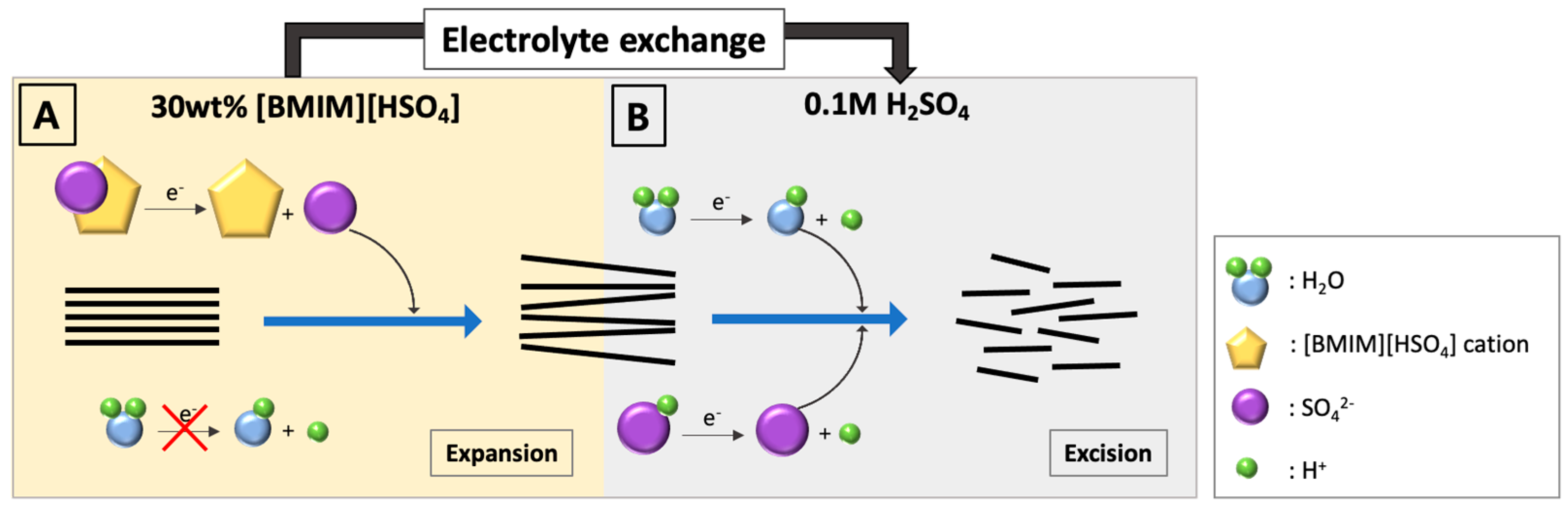
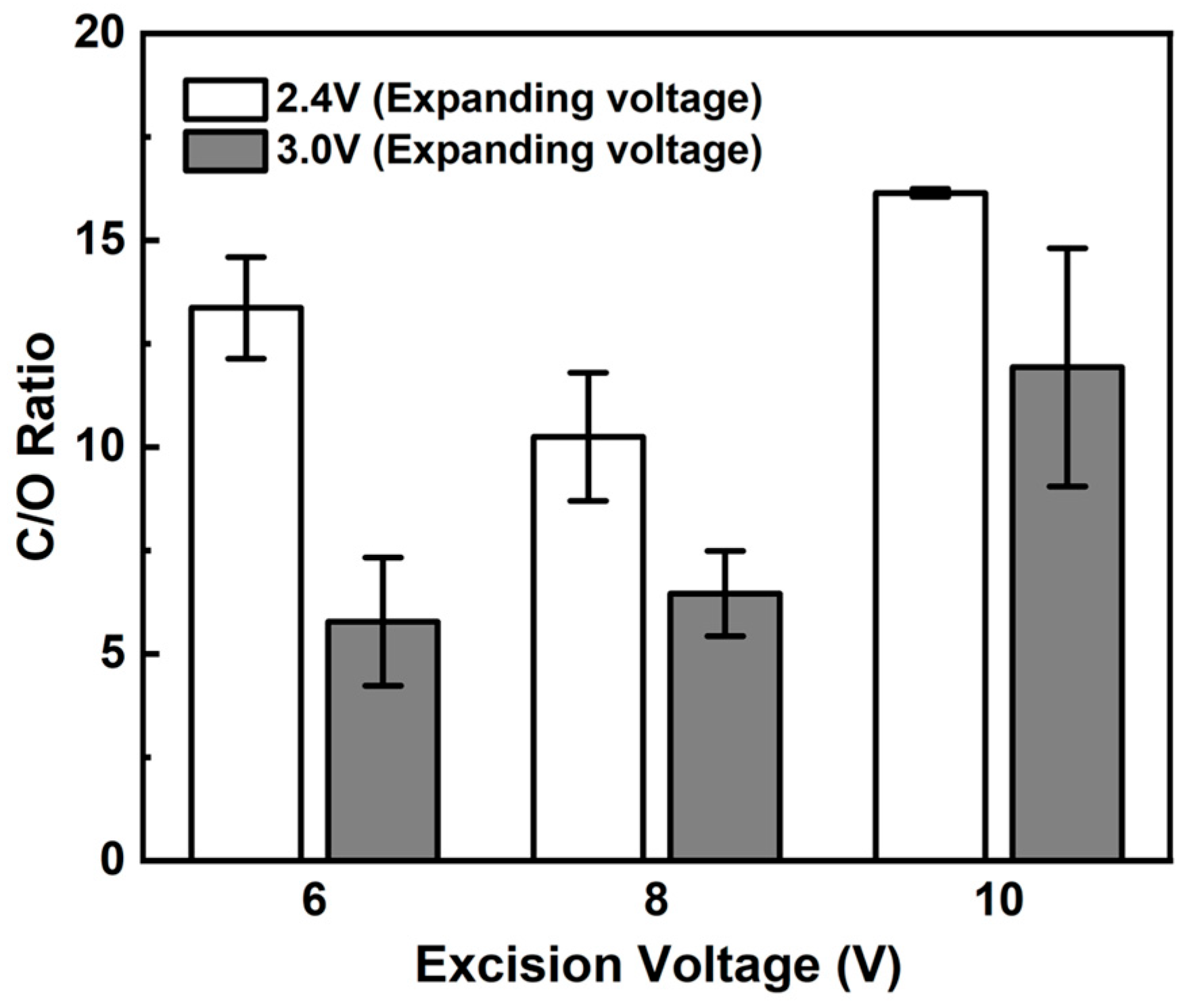
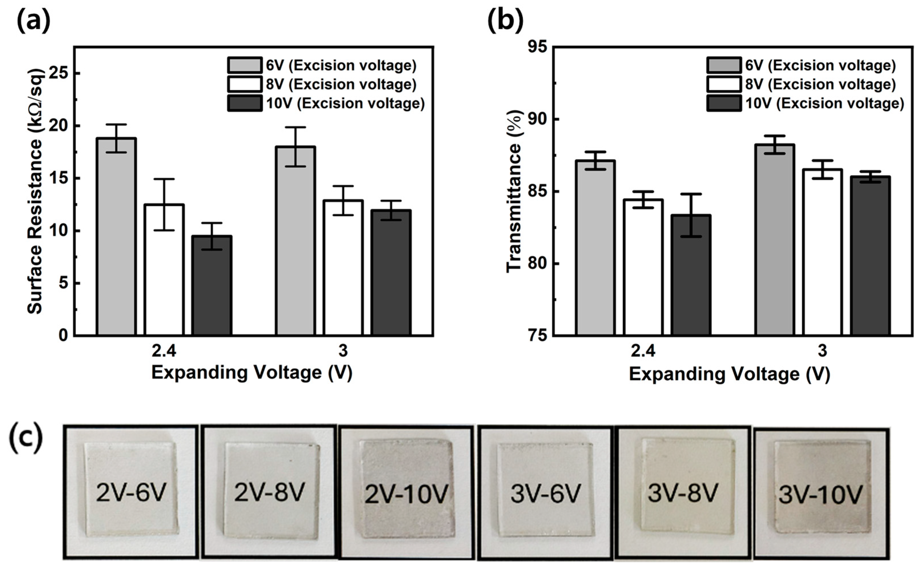
3.1. Electrochemical Exfoliation
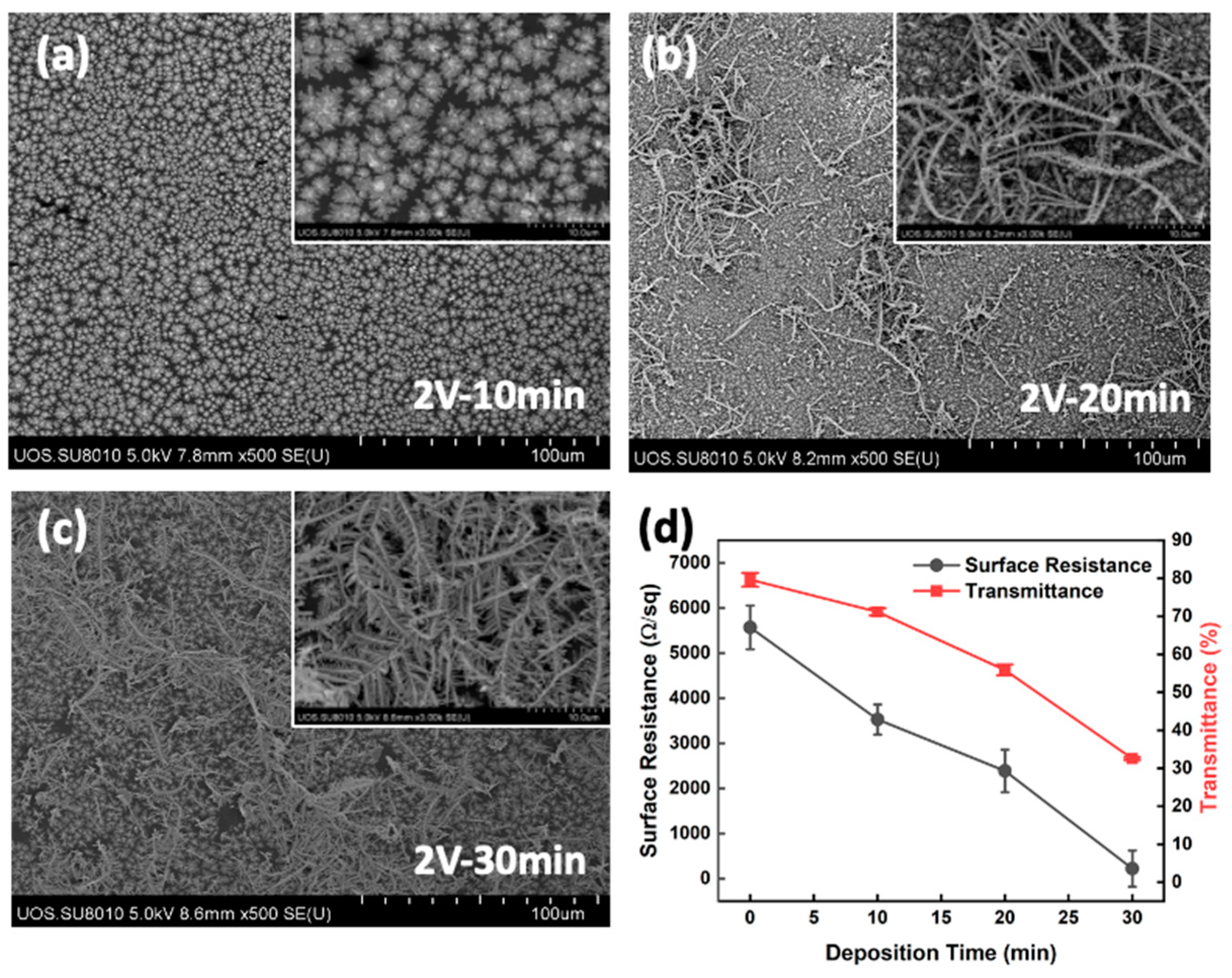
3.2. Layer Stacking and Electro-Deposition of Silver
4. Conclusions
5. Future Works
Supplementary Materials
Author Contributions
Funding
Data Availability Statement
Conflicts of Interest
References
- Rani, P.; Jindal, V.K. Designing Band Gap of Graphene by B and N Dopant Atoms. RSC Adv. 2013, 3, 802–812. [Google Scholar] [CrossRef]
- Phiri, J.; Gane, P.; Maloney, T.C. General Overview of Graphene: Production, Properties and Application in Polymer Composites. Mater. Sci. Eng. B Solid State Mater. Adv. Technol. 2017, 215, 9–28. [Google Scholar] [CrossRef]
- Zhu, Y.; Ji, H.; Cheng, H.; Ruoff, R.S. Mass Production and Industrial Applications of Graphene Materials. Natl. Sci. Rev. 2018, 90–101. [Google Scholar] [CrossRef]
- Plutnar, J.; Pumera, M.; Sofer, Z. The Chemistry of CVD Graphene. J. Mater. Chem. C Mater. 2018, 6, 6082–6101. [Google Scholar] [CrossRef]
- Park, S.; An, J.; Jung, I.; Piner, R.D.; An, S.J.; Li, X.; Velamakanni, A.; Ruoff, R.S. Colloidal Suspensions of Highly Reduced Graphene Oxide in a Wide Variety of Organic Solvents. Nano Lett. 2009, 9, 1593–1597. [Google Scholar] [CrossRef] [PubMed]
- Wang, S.; Ang, P.K.; Wang, Z.; Tang, A.L.L.; Thong, J.T.L.; Loh, K.P. High Mobility, Printable, and Solution-Processed Graphene Electronics. Nano Lett. 2010, 10, 92–98. [Google Scholar] [CrossRef] [PubMed]
- Xin, G.; Yao, T.; Sun, H.; Scott, S.M.; Shao, D.; Wang, G.; Lian, J. Highly Thermally Conductive and Mechanically Strong Graphene Fibers. Science 2015, 349, 1083–1087. [Google Scholar] [CrossRef] [PubMed]
- Ahn, H.S.; Kim, J.M.; Kim, T.; Park, S.C.; Kim, J.M.; Park, Y.; Yu, D.I.; Hwang, K.W.; Jo, H.; Park, H.S.; et al. Enhanced Heat Transfer Is Dependent on Thickness of Graphene Films: The Heat Dissipation during Boiling. Sci. Rep. 2014, 4, srep06276. [Google Scholar] [CrossRef] [PubMed]
- Surwade, S.P.; Smirnov, S.N.; Vlassiouk, I.V.; Unocic, R.R.; Veith, G.M.; Dai, S.; Mahurin, S.M. Water Desalination Using Nanoporous Single-Layer Graphene. Nat. Nanotechnol. 2015, 10, 459–464. [Google Scholar] [CrossRef]
- Dervin, S.; Dionysiou, D.D.; Pillai, S.C. 2D Nanostructures for Water Purification: Graphene and Beyond. Nanoscale 2016, 8, 15115–15131. [Google Scholar] [CrossRef]
- Xia, Z.Y.; Pezzini, S.; Treossi, E.; Giambastiani, G.; Corticelli, F.; Morandi, V.; Zanelli, A.; Bellani, V.; Palermo, V. The Exfoliation of Graphene in Liquids by Electrochemical, Chemical, and Sonication-Assisted Techniques: A Nanoscale Study. Adv. Funct. Mater. 2013, 23, 4684–4693. [Google Scholar] [CrossRef]
- Yang, Y.; Hou, H.; Zou, G.; Shi, W.; Shuai, H.; Li, J.; Ji, X. Electrochemical Exfoliation of Graphene-like Two-Dimensional Nanomaterials. Nanoscale 2019, 11, 16–33. [Google Scholar] [CrossRef]
- Coleman, J.N. Liquid Exfoliation of Defect-Free Graphene. Acc. Chem. Res. 2013, 46, 14–22. [Google Scholar] [CrossRef]
- Xu, Y.; Cao, H.; Xue, Y.; Li, B.; Cai, W. Liquid-Phase Exfoliation of Graphene: An Overview on Exfoliation Media, Techniques, and Challenges. Nanomaterials 2018, 8, 942. [Google Scholar] [CrossRef]
- Liu, F.; Wang, C.; Sui, X.; Riaz, M.A.; Xu, M.; Wei, L.; Chen, Y. Synthesis of Graphene Materials by Electrochemical Exfoliation: Recent Progress and Future Potential. Carbon. Energy 2019, 1, 173–199. [Google Scholar] [CrossRef]
- Du, W.; Jiang, X.; Zhu, L. From Graphite to Graphene: Direct Liquid-Phase Exfoliation of Graphite to Produce Single- and Few-Layered Pristine Graphene. J. Mater. Chem. A Mater. 2013, 1, 10592–10606. [Google Scholar] [CrossRef]
- Wang, G.; Wang, B.; Park, J.; Wang, Y.; Sun, B.; Yao, J. Highly Efficient and Large-Scale Synthesis of Graphene by Electrolytic Exfoliation. Carbon 2009, 47, 3242–3246. [Google Scholar] [CrossRef]
- Tyurnina, A.V.; Tzanakis, I.; Morton, J.; Mi, J.; Porfyrakis, K.; Maciejewska, B.M.; Grobert, N.; Eskin, D.G. Ultrasonic Exfoliation of Graphene in Water: A Key Parameter Study. Carbon 2020, 168, 737–747. [Google Scholar] [CrossRef]
- Hou, Y.; Lv, S.; Liu, L.; Liu, X. High-Quality Preparation of Graphene Oxide via the Hummers’ Method: Understanding the Roles of the Intercalator, Oxidant, and Graphite Particle Size. Ceram. Int. 2020, 46, 2392–2402. [Google Scholar] [CrossRef]
- Ciesielski, A.; Samorì, P. Grapheneviasonication Assisted Liquid-Phase Exfoliation. Chem. Soc. Rev. 2014, 43, 381–398. [Google Scholar] [CrossRef]
- Yu, P.; Lowe, S.E.; Simon, G.P.; Zhong, Y.L. Electrochemical Exfoliation of Graphite and Production of Functional Graphene. Curr. Opin. Colloid. Interface Sci. 2015, 20, 329–338. [Google Scholar] [CrossRef]
- Liu, W.W.; Aziz, A. Review on the Effects of Electrochemical Exfoliation Parameters on the Yield of Graphene Oxide. ACS Omega 2022, 7, 33719–33731. [Google Scholar] [CrossRef] [PubMed]
- Brownson, D.A.C.; Metters, J.P.; Kampouris, D.K.; Banks, C.E. Graphene Electrochemistry: Surfactants Inherent to Graphene Can Dramatically Effect Electrochemical Processes. Electroanalysis 2011, 23, 894–899. [Google Scholar] [CrossRef]
- Alanyalıoğlu, M.; Segura, J.J.; Oro-Sole, J.; Casan-Pastor, N. The Synthesis of Graphene Sheets with Controlled Thickness and Order Using Surfactant-Assisted Electrochemical Processes. Carbon 2012, 50, 142–152. [Google Scholar] [CrossRef]
- Lim, S.; Han, J.H.; Kang, H.W.; Lee, J.U.; Lee, W. Preparation of Electrochemically Exfoliated Graphene Sheets Using DC Switching Voltages. Carbon. Lett. 2020, 30, 409–416. [Google Scholar] [CrossRef]
- Hsieh, C.-T.; Hsueh, J.-H. Electrochemical Exfoliation of Graphene Sheets from a Natural Graphite Flask in the Presence of Sulfate Ions at Different Temperatures. RSC Adv. 2016, 6, 64826–64831. [Google Scholar] [CrossRef]
- Zhang, Y.; Xu, Y.; Niu, Y.; Hou, W.; Liu, R. Highly Efficient Dual-Electrode Exfoliation of Graphite into High-Quality Graphene via Square-Wave Alternating Currents. Chem. Eng. J. 2023, 456, 140977. [Google Scholar] [CrossRef]
- Zhang, Y.; Xu, Y.; Liu, R. Regulating Cations and Solvents of the Electrolyte for Ultra-Efficient Electrochemical Production of High-Quality Graphene. Carbon 2021, 176, 157–167. [Google Scholar] [CrossRef]
- Wang, J.; Manga, K.K.; Bao, Q.; Loh, K.P. High-Yield Synthesis of Few-Layer Graphene Flakes through Electrochemical Expansion of Graphite in Propylene Carbonate Electrolyte. J. Am. Chem. Soc. 2011, 133, 8888–8891. [Google Scholar] [CrossRef] [PubMed]
- Ambrosi, A.; Chua, C.K.; Bonanni, A.; Pumera, M. Electrochemistry of Graphene and Related Materials. Chem. Rev. 2014, 114, 7150–7188. [Google Scholar] [CrossRef]
- Yang, S.; Brüller, S.; Wu, Z.S.; Liu, Z.; Parvez, K.; Dong, R.; Richard, F.; Samorì, P.; Feng, X.; Müllen, K. Organic Radical-Assisted Electrochemical Exfoliation for the Scalable Production of High-Quality Graphene. J. Am. Chem. Soc. 2015, 137, 13927–13932. [Google Scholar] [CrossRef] [PubMed]
- Li, L.; Wang, M.; Guo, J.; Cao, M.; Qiu, H.; Dai, L.; Yang, Z. Regulation of Radicals from Electrochemical Exfoliation of a Double-Graphite Electrode to Fabricate High-Quality Graphene. J. Mater. Chem. C Mater. 2018, 6, 6257–6263. [Google Scholar] [CrossRef]
- Seo, S.; Min, M.; Lee, J.; Lee, T.; Choi, S.; Lee, H. Solution-Processed Reduced Graphene Oxide Films as Electronic Contacts for Molecular Monolayer Junctions. Angew. Chem. Int. Ed. 2011, 51, 108–112. [Google Scholar] [CrossRef] [PubMed]
- Gabbett, C.; Kelly, A.G.; Coleman, E.; Doolan, L.; Carey, T.; Synnatschke, K.; Liu, S.; Dawson, A.; O’Suilleabhain, D.; Munuera, J.; et al. Understanding How Junction Resistances Impact the Conduction Mechanism in Nano-Networks. Nat. Commun. 2024, 15, 4517. [Google Scholar] [CrossRef]
- Li, H.; Liu, Y.; Su, A.; Wang, J.; Duan, Y. Promising Hybrid Graphene-Silver Nanowire Composite Electrode for Flexible Organic Light-Emitting Diodes. Sci. Rep. 2019, 9, 17998. [Google Scholar] [CrossRef]
- Lee, K.E.; Kim, J.E.; Maiti, U.N.; Lim, J.; Hwang, J.O.; Shim, J.; Oh, J.J.; Yun, T.; Kim, S.O. Liquid Crystal Size Selection of Large-Size Graphene Oxide for Size-Dependent N-Doping and Oxygen Reduction Catalysis. ACS Nano 2014, 8, 9073–9080. [Google Scholar] [CrossRef] [PubMed]
- Kim, M.; Nabeya, S.; Han, S.-M.; Kim, M.-S.; Lee, S.; Kim, H.-M.; Cho, S.-Y.; Lee, D.-J.; Kim, S.-H.; Kim, K.-B. Selective Atomic Layer Deposition of Metals on Graphene for Transparent Conducting Electrode Application. ACS Appl. Mater. Interfaces 2020, 12, 14331–14340. [Google Scholar] [CrossRef] [PubMed]
- Qian, Y.; Zhou, C.; Zhou, J.; Huang, A. Synthesis of Silver-Nanoparticles Composite with Highly Catalytic Activity Supported on the Reduced Graphene Oxide. Appl Surf Sci 2020, 525, 146597. [Google Scholar] [CrossRef]
- Rao, K.S.; Senthilnathan, J.; Liu, Y.F.; Yoshimura, M. Role of Peroxide Ions in Formation of Graphene Nanosheets by Electrochemical Exfoliation of Graphite. Sci. Rep. 2014, 4, 4237. [Google Scholar] [CrossRef]
- Shim, J.; Yun, J.M.; Yun, T.; Kim, P.; Lee, K.E.; Lee, W.J.; Ryoo, R.; Pine, D.J.; Yi, G.R.; Kim, S.O. Two-Minute Assembly of Pristine Large-Area Graphene Based Films. Nano Lett. 2014, 14, 1388–1393. [Google Scholar] [CrossRef]
- O’Mahony, A.M.; Silvester, D.S.; Aldous, L.; Hardacre, C.; Compton, R.G. Effect of Water on the Electrochemical Window and Potential Limits of Room-Temperature Ionic Liquids. J. Chem. Eng. Data 2008, 53, 2884–2891. [Google Scholar] [CrossRef]
- Hayyan, M.; Mjalli, F.S.; Hashim, M.A.; AlNashef, I.M.; Mei, T.X. Investigating the Electrochemical Windows of Ionic Liquids. J. Ind. Eng. Chem. 2013, 19, 106–112. [Google Scholar] [CrossRef]
- Ravula, S.; Baker, S.N.; Kamath, G.; Baker, G.A. Ionic Liquid-Assisted Exfoliation and Dispersion: Stripping Graphene and Its Two-Dimensional Layered Inorganic Counterparts of Their Inhibitions. Nanoscale 2015, 7, 4338–4353. [Google Scholar] [CrossRef] [PubMed]
- Matsumoto, M.; Saito, Y.; Park, C.; Fukushima, T.; Aida, T. Ultrahigh-Throughput Exfoliation of Graphite into Pristine “single-Layer” Graphene Using Microwaves and Molecularly Engineered Ionic Liquids. Nat. Chem. 2015, 7, 730–736. [Google Scholar] [CrossRef] [PubMed]
- Greer, A.J.; Jacquemin, J.; Hardacre, C. Industrial Applications of Ionic Liquids. Molecules 2020, 25, 5207. [Google Scholar] [CrossRef]
- Tarcan, R.; Handrea-Dragan, M.; Todor-Boer, O.; Petrovai, I.; Farcau, C.; Rusu, M.; Vulpoi, A.; Todea, M.; Astilean, S.; Botiz, I. A New, Fast and Facile Synthesis Method for Reduced Graphene Oxide in N,N-Dimethylformamide. Synth. Met. 2020, 269, 116576. [Google Scholar] [CrossRef]
- Dubin, S.; Gilje, S.; Wang, K.; Tung, V.C.; Cha, K.; Hall, A.S.; Farrar, J.; Varshneya, R.; Yang, Y.; Kaner, R.B. A One-Step, Solvothermal Reduction Method for Producing Reduced Graphene Oxide Dispersions in Organic Solvents. ACS Nano 2010, 4, 3845–3852. [Google Scholar] [CrossRef] [PubMed]
- Hofmann, M.; Chiang, W.-Y.; Nguyễn, T.D.; Hsieh, Y.-P. Controlling the Properties of Graphene Produced by Electrochemical Exfoliation. Nanotechnology 2015, 26, 335607. [Google Scholar] [CrossRef] [PubMed]
- Malard, L.M.; Pimenta, M.A.; Dresselhaus, G.; Dresselhaus, M.S. Raman Spectroscopy in Graphene. Phys. Rep. 2009, 473, 51–87. [Google Scholar] [CrossRef]
- Wall, M. Raman spectroscopy optimizes graphene characterization. AM & P 2012, 170, 35–38. [Google Scholar] [CrossRef]
- Barwich, S.; Medeiros de Araújo, J.; Rafferty, A.; Gomes da Rocha, C.; Ferreira, M.S.; Coleman, J.N. On the Relationship between Morphology and Conductivity in Nanosheet Networks. Carbon 2021, 171, 306–319. [Google Scholar] [CrossRef]
- Xie, J.; Zeng, Y.; Yang, X.; Xu, X. Electrodeposition of Silver Dendritic-Graphene Composite Film for Photocatalytic Application. Int. J. Electrochem. Sci. 2017, 12, 1690–1699. [Google Scholar] [CrossRef]
- Wierzbicki, M.; Jaworski, S.; Sawosz, E.; Jung, A.; Gielerak, G.; Jaremek, H.; Łojkowski, W.; Woźniak, B.; Stobiński, L.; Małolepszy, A.; et al. Graphene Oxide in a Composite with Silver Nanoparticles Reduces the Fibroblast and Endothelial Cell Cytotoxicity of an Antibacterial Nanoplatform. Nanoscale Res. Lett. 2019, 14, 320. [Google Scholar] [CrossRef] [PubMed]
- Zhong, L.; Gan, S.; Fu, X.; Li, F.; Han, D.; Guo, L.; Niu, L. Electrochemically Controlled Growth of Silver Nanocrystals on Graphene Thin Film and Applications for Efficient Nonenzymatic H2O2 Biosensor. Electrochim. Acta 2013, 89, 222–228. [Google Scholar] [CrossRef]
- Majidi, M.R.; Ghaderi, S.; Asadpour-Zeynali, K.; Dastangoo, H. Synthesis of Dendritic Silver Nanostructures Supported by Graphene Nanosheets and Its Application for Highly Sensitive Detection of Diazepam. Mater. Sci. Eng. C 2015, 57, 257–264. [Google Scholar] [CrossRef]


| Ionic Liquid Concentrations (%) | Initial pH | Applied Voltage (V) | Final pH |
|---|---|---|---|
| 10 | 1.3 | 1.9 | 1.26 |
| 20 | 1.18 | 2.1 | 1.25 |
| 30 | 1.08 | 2.4 | 1.19 |
| 40 | 1.04 | 2.7 | 1.05 |
| 50 | 1.01 | 3 | 1.03 |
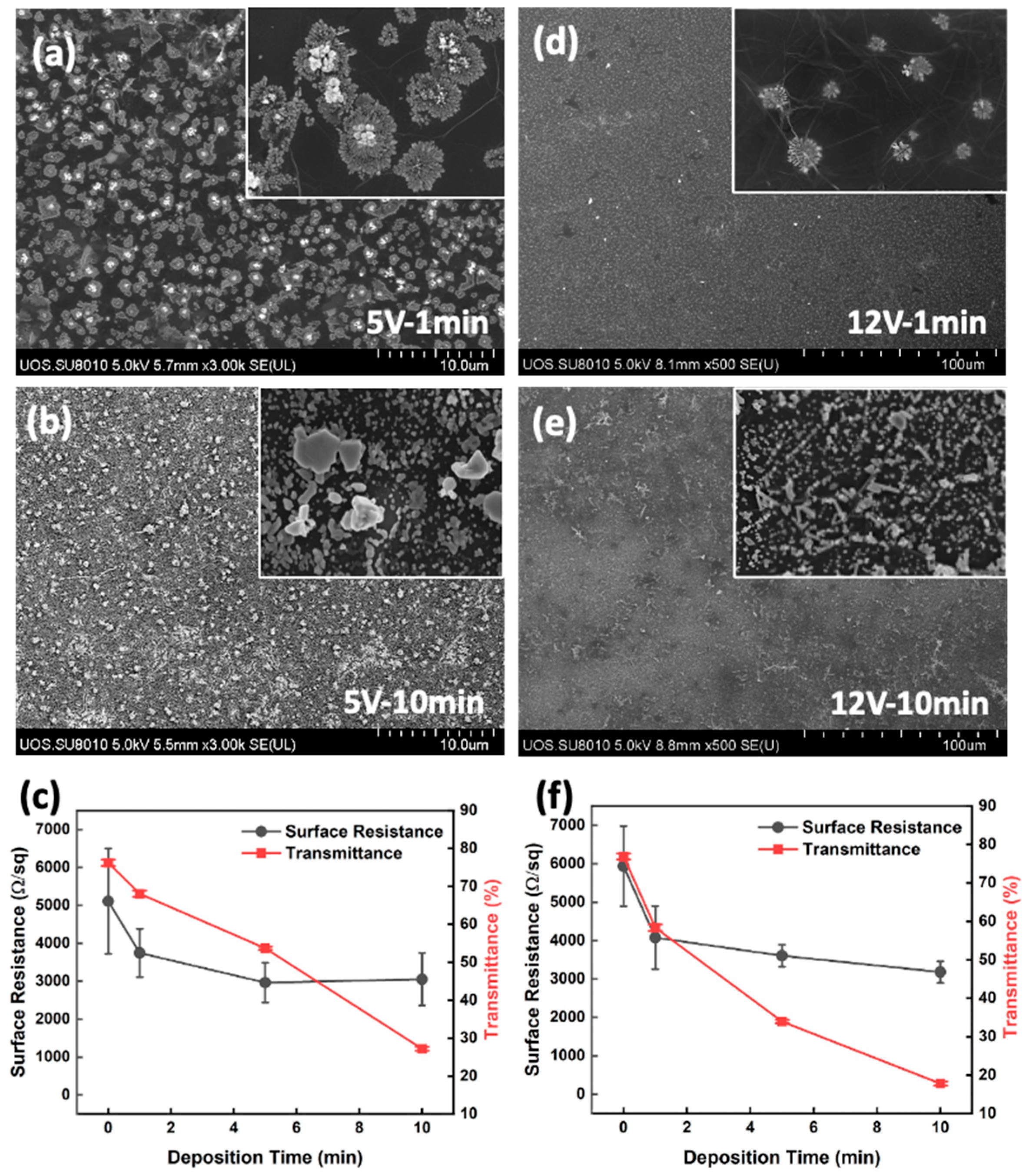
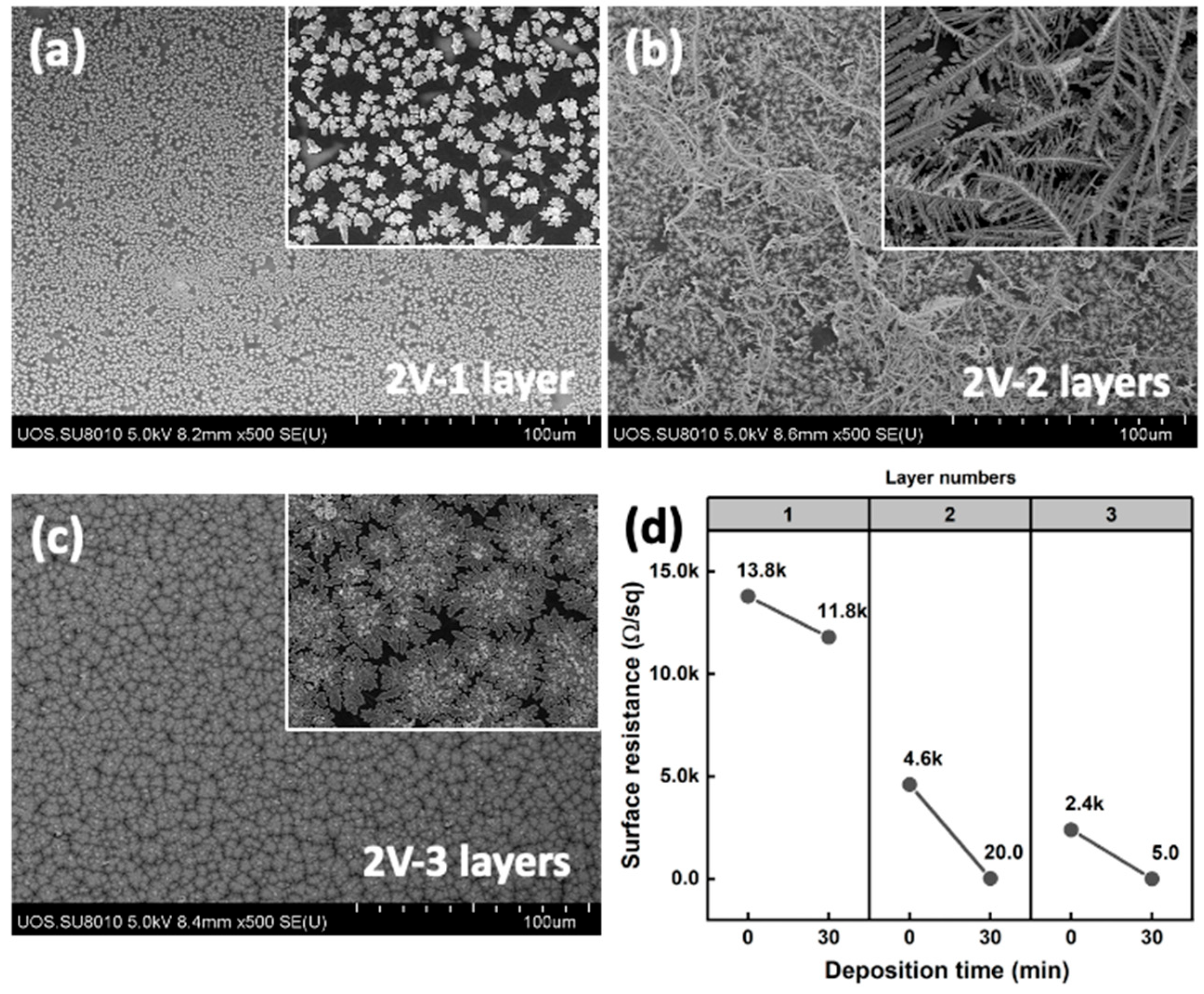
| Ion Concentration (M) | Deposition Voltage (V) | Electrode Area (cm2) | Surface Resistance (KΩ/sq) | Current Density (mA/cm2) |
|---|---|---|---|---|
| 1 × 10⁻⁴ | 2 | 2.25 (1 L) | 14 | 0.31 |
| 1 × 10⁻⁴ | 5 | 2.25 (1 L) | 14 | 1.26 |
| 1 × 10⁻⁴ | 12 | 2.25 (1 L) | 14 | 3.48 |
| 1 × 10⁻⁴ | 2 | 2.25 (2 L) | 5.5 | 0.78 |
| 1 × 10⁻⁴ | 5 | 2.25 (2 L) | 5.1 | 3.45 |
| 1 × 10⁻⁴ | 12 | 2.25 (2 L) | 4.3 | 11.33 |
| 1 × 10⁻³ | 2 | 2.25 (1 L) | 13.8 | 0.33 |
| 1 × 10⁻³ | 2 | 2.25 (2 L) | 4.6 | 0.99 |
| 1 × 10⁻³ | 2 | 2.25 (3 L) | 2.6 | 1.75 |
Disclaimer/Publisher’s Note: The statements, opinions and data contained in all publications are solely those of the individual author(s) and contributor(s) and not of MDPI and/or the editor(s). MDPI and/or the editor(s) disclaim responsibility for any injury to people or property resulting from any ideas, methods, instructions or products referred to in the content. |
© 2024 by the authors. Licensee MDPI, Basel, Switzerland. This article is an open access article distributed under the terms and conditions of the Creative Commons Attribution (CC BY) license (https://creativecommons.org/licenses/by/4.0/).
Share and Cite
Bak, S.; Shim, J. Study of Morphology Control of Electro-Deposited Silver on Electro-Chemically Exfoliated Graphene Electrode and Its Conductivity. Materials 2024, 17, 2988. https://doi.org/10.3390/ma17122988
Bak S, Shim J. Study of Morphology Control of Electro-Deposited Silver on Electro-Chemically Exfoliated Graphene Electrode and Its Conductivity. Materials. 2024; 17(12):2988. https://doi.org/10.3390/ma17122988
Chicago/Turabian StyleBak, Siwon, and Jongwon Shim. 2024. "Study of Morphology Control of Electro-Deposited Silver on Electro-Chemically Exfoliated Graphene Electrode and Its Conductivity" Materials 17, no. 12: 2988. https://doi.org/10.3390/ma17122988