Article

Analysis of Carrier Transport at Zn1−xSnxOy/Absorber Interface in Sb2(S,Se)3 Solar Cells

1
International School of Microelectronics, Dongguan University of Technology, Dongguan 523000, China
2
School of Computer Science and Technology, Dongguan University of Technology, Dongguan 523000, China
3
Shenzhen Key Laboratory of Advanced Thin Films and Applications, Key Laboratory of Optoelectronic Devices and Systems of Ministry of Education and Guangdong Province, State Key Laboratory of Radio Frequency Heterogeneous Integration, College of Physics and Optoelectronic Engineering, Shenzhen University, Shenzhen 518060, China
*
Authors to whom correspondence should be addressed.
Materials 2024, 17(13), 3214; https://doi.org/10.3390/ma17133214
Submission received: 25 May 2024 / Revised: 17 June 2024 / Accepted: 26 June 2024 / Published: 1 July 2024
(This article belongs to the Section Optical and Photonic Materials)

Abstract

:
This work explores the effect of a Zn1−xSnxOy (ZTO) layer as a potential replacement for CdS in Sb2(S,Se)3 devices. Through the use of Afors-het software v2.5, it was determined that the ZTO/Sb2(S,Se)3 interface exhibits a lower conduction band offset (CBO) value of 0.34 eV compared to the CdS/Sb2(S,Se)3 interface. Lower photo-generated carrier recombination can be obtained at the interface of the ZTO/Sb2(S,Se)3 heterojunction. In addition, the valence band offset (VBO) value at the ZTO/Sb2(S,Se)3 interface increases to 1.55 eV. The ZTO layer increases the efficiency of the device from 7.56% to 11.45%. To further investigate the beneficial effect of the ZTO layer on the efficiency of the device, this goal has been achieved by five methods: changing the S content of the absorber, changing the thickness of the absorber, changing the carrier concentration of ZTO, using various Sn/(Zn+Sn) ratios in ZTO, and altering the thickness of the ZTO layer. When the S content in Sb2(S,Se)3 is around 60% and the carrier concentration is about 1018 cm−3, the efficiency is optimal. The optimal thickness of the Sb2(S,Se)3 absorber layer is 260 nm. A ZTO/Sb2(S,Se)3 interface with a Sn/(Zn+Sn) ratio of 0.18 exhibits a better CBO value. It is also found that a ZTO thickness of 20 nm is needed for the best efficiency.

1. Introduction

In recent years, Sb2(S,Se)3 has been regarded as a potential semiconductor thin film among new-type photovoltaic materials due to its excellent stability, ideal band gap, and suitable absorption coefficient [1,2,3,4]. Sb2(S,Se)3 is deposited using different technologies, such as vapor transport deposition, rapid thermal evaporation, pulsed laser deposition, hydrothermal methods, spin-coating, and chemical bath deposition [5,6,7,8,9,10]. In 2019, Tang’s group fabricated Sb2(S,Se)3 devices using rapid thermal evaporation and vapor transport deposition. The best efficiency of the devices was less than 7% [5]. Chen et al. prepared an Sb2(S,Se)3 device with an efficiency of 7.05% by pulsed laser deposition in 2020 [7]. Recently, solution synthesis processes have also contributed to the deposition of Sb2(S,Se)3 for high-photovoltaic-performance Sb2(S,Se)3 devices. In 2021, Li et al. used hydrothermal technology to deposit Sb2(S,Se)3 on devices. They achieved a maximum efficiency of 10.7% [11]. Thus, the solution synthesis method is better than the vacuum method.
Despite the benefits of the hydrothermal method in preparing high-PCE devices, understanding the growth mechanism of the Sb2(S,Se)3 absorber layer using this technique is challenging. This difficulty primarily arises from the inability to monitor important factors, such as chemical reactions within the hydrothermal solution, temperature, and pH. Furthermore, synthesizing large-scale-area solar cells using this method poses a significant challenge. Therefore, it is urgent to explore a new solution method that involves high-quality preparation, is monitorable, and uses large grain sizes to prepare Sb2(S,Se)3 devices. CBD technology is an excellent choice for producing Sb2(S,Se)3 photovoltaic devices, as it offers several advantages over the hydrothermal process. These advantages include (i) the ability to synthesize devices at low temperatures, (ii) the real-time monitoring of precursors to understand the growth mechanism of the absorber layer, (iii) the capability to fabricate devices over large areas, and (iv) the potential for V-shaped band-gap engineering [10]. In 2022, Tang’s group prepared Sb2(S,Se)3 devices using CBD technology, and the efficiency of the device reached 8.27% [10]. This is the highest PCE achieved for Sb2(S,Se)3 devices through the CBD method. However, the best PCE of a device using the CBD method is still below the Shockley–Queisser (SQ) limit. Therefore, further optimization of the photovoltaic properties of the devices is needed.
The high-efficiency devices utilized a CdS buffer layer. The cliff-like conduction band offset (CBO) values of the CdS/Sb2Se3 interface are negative in Sb2Se3-based devices, producing high recombination losses at the interface [10,12,13]. The Sb2(S,Se)3 material is similar to Sb2Se3, and a cliff-like CBO may develop at the interface between CdS and Sb2(S,Se)3. Thus, the CdS/Sb2(S,Se)3 interface plays a critical role in determining the photovoltaic properties of Sb2(S,Se)3 devices. It is essential to optimize the CdS/Sb2(S,Se)3 interface to enhance the efficiency of an Sb2(S,Se)3 device. In this study, we introduce the use of a Cd-free buffer layer consisting of Zn1−xSnxOy (ZTO) as a replacement for the CdS layer utilizing Afors-het software for the first time. The work is divided into five steps: (I) replacing the CdS buffer layer with the ZTO ternary compound and evaluating its impact on the efficiency of the devices, (II) varying the S content in Sb2(S,Se)3 and studying its effect on the efficiency, (III) studying the effect of the thickness of Sb2(S,Se)3 on the efficiency of the device, (IV) investigating the impact of the carrier concentration of ZTO on the PCE of devices, and (V) analyzing the effect of ZTO’s Sn/(Zn+Sn) ratio and thickness on the device’s efficiency. This work presents a novel approach to enhancing the efficiency of devices and serves as a valuable experimental guide.

2. Methods

The Afors-het program was used to analyze the impact of the ZTO layer on the efficiency of an Sb2(S,Se)3 device. The fundamental semiconductor equations employed for the semiconductor device include the Poisson equation, equations for hole and electron current densities, and electron and hole continuity equations:
J n = q μ n n E E n x ; J p = q μ p p E E p x
x ( ε ϕ x ) = q ε 0 ( n + p N A + N D + + n t + p t )
n t = G R n + μ n E x n x + D n 2 n x 2 ; p t = G R p + μ p E x p x + D p 2 p x 2
where ε and q are the dielectric constant and the electron charge, N A and N D + are ionized acceptor and donor concentrations, and p and n are hole and electron concentrations. ϕ , μ p , and μ n are the electrostatic potential, the hole’s mobility, and the electron’s mobility, respectively. J p and J n are the hole’s current density and the electron’s current density. E F n and E F p are the electron quasi-Fermi level and hole quasi-Fermi level, respectively. G , D n , and D p are the generation rate, the electron’s diffusion coefficient, and the hole’s diffusion coefficient, respectively. E x , R n , and R P are the electric field, the recombination rate of electrons, and the recombination rate of holes, respectively. Figure 1 displays the simulated device structures with CdS and ZTO electron transport layers. Table 1 and Table 2 list the simulated parameters of the Sb2(S,Se)3 device with a superstrate structure [14,15,16,17,18,19,20].
To further study the carrier transport between ZTO and Sb2(S,Se)3, four methods were analyzed. Firstly, the effect of the absorber’s S content on the efficiency of Sb2(S,Se)3 devices was calculated. Secondly, the impact of the thickness of the Sb2(S,Se)3 layer on the PCE of the device was investigated. Thirdly, the influence of the ZTO layer’s carrier concentration on the efficiency of the device was examined. Fourthly, the effect of the ZTO layer with varying Sn/(Zn+Sn) ratios on the PCE of the device was analyzed. Lastly, the impact of the thickness of the ZTO layer on the device’s efficiency was investigated. In this study, the band gap of the absorber layer was varied from 1.2 to 1.7 eV to implement the first method. Previous research has shown that the absorber’s band gap decreases linearly with a decrease in the sulfur mole fraction [21]. Figure 2 illustrates the relationship between the S content of the absorber layer and the band gap of the absorber layer, which was used to analyze the effect of the S content on the efficiency of the device. The absorber carrier concentration changes from 1 × 1015 cm−3 to 1 × 1021 cm−3. Additionally, Lee et al. suggested that the band gap and electron affinity of the ZTO layer change based on the Sn/(Zn+Sn) ratio [22]. The relationship between the band gap of the ZTO layer, electron affinity, and Sn/(Zn+Sn) ratio is depicted in Figure 3, which was used to analyze the impact of different Sn/(Zn+Sn) ratios on the PCE of solar cells. To study the effect of ZTO thickness on the device’s PCE, the thickness was changed from 10 nm to 100 nm.

3. Results and Discussion

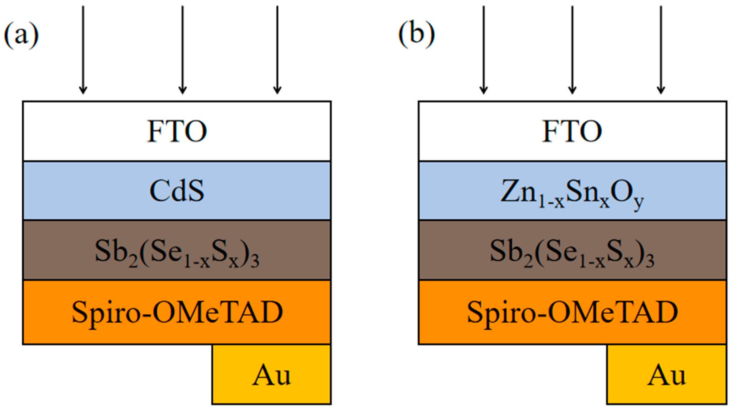
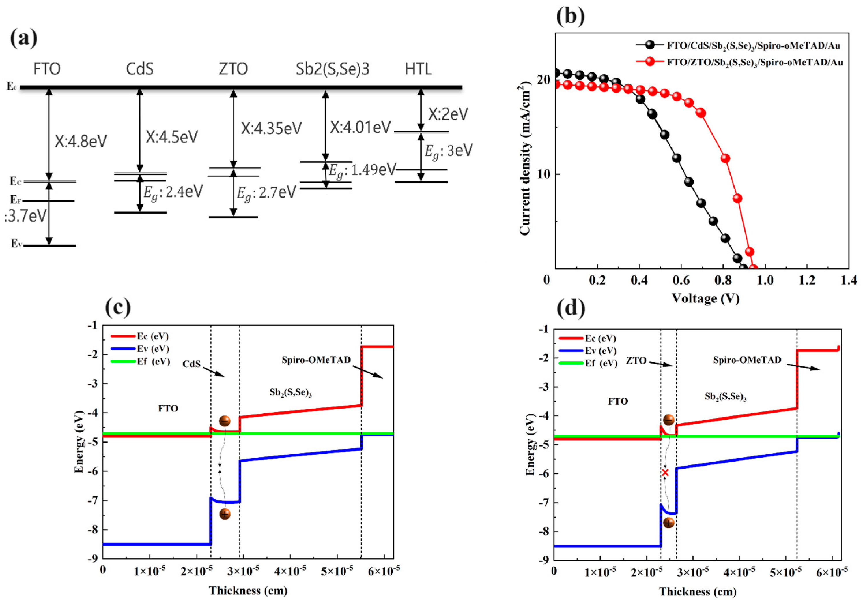
3.1. Impact of ZTO Layer

Before investigating the impact of the ZTO layer, it is important to optimize the thickness of the Sb2(S,Se)3 layer. The thickness of the Sb2(S,Se)3 layer was varied from 100 nm to 420 nm. The results in Figure 4 demonstrate the influence of the Sb2(S,Se)3 layer thickness on the photovoltaic parameters of CdS/Sb2(S,Se)3 solar cells. The thickness of the Sb2(S,Se)3 layer increases from 100 nm to 420 nm, resulting in a decrease in VOC from 0.916 V to 0.887 V. However, JSC increases from 12.95 mA/cm2 to 23.81 mA/cm2 with the thicker Sb2(S,Se)3 layer. The FF of the Sb2(S,Se)3 device decreases from 53.04% to 35.29% as the thickness of the Sb2(S,Se)3 layer increases. The efficiency of the Sb2(S,Se)3 device improves from 6.29% to 7.56% when the thickness of the Sb2(S,Se)3 layer increases from 100 nm to 260 nm, but it then decreases to 7.45% with a further thickness increase. The optimal thickness of the Sb2(S,Se)3 layer is 260 nm in the CdS/Sb2(S,Se)3 device. Figure 5 illustrates the comparison of CdS and ZTO layers in Sb2(S,Se)3 devices as electron transport layers (ETLs) based on the ideal thickness of the Sb2(S,Se)3 layer. Figure 5a displays the band gap and electron affinity of each layer in the devices. The J-V curves of devices with various ETLs are shown in Figure 5b. The device with a CdS layer achieved a PCE of 7.56%, with a VOC of 0.896 V, a JSC of 20.75 mA/cm2, and an FF of 40.61%. In comparison, the Sb2(S,Se)3 device with ZTO demonstrated a higher VOC of 0.942 V, a JSC of 19.56 mA/cm2, an FF of 62.14%, and an efficiency of 11.45%, indicating improved photovoltaic properties. Figure 5c,d depict the energy band diagrams of devices with CdS and ZTO buffer layers. The CBO value at the interface between CdS and Sb2(S,Se)3 was 0.49 eV, while with ZTO, it decreased to 0.34 eV, suggesting easier electron flow from ZTO to Sb2(S,Se)3 and reduced carrier recombination (The symbol "X" signifies the decreased carrier recombination). The VBO value at the ZTO/Sb2(S,Se)3 interface was 1.55 eV, which is higher than the 1.40 eV VBO value at the interface of CdS/Sb2(S,Se)3. The improved CBO and VBO values at the interface enhance the carrier collection and VOC of the Sb2(S,Se)3 device, consistent with the J-V results.

3.2. Analysis of Photo-Generated Carrier Collection at ZTO/Sb2(S,Se)3 Interface

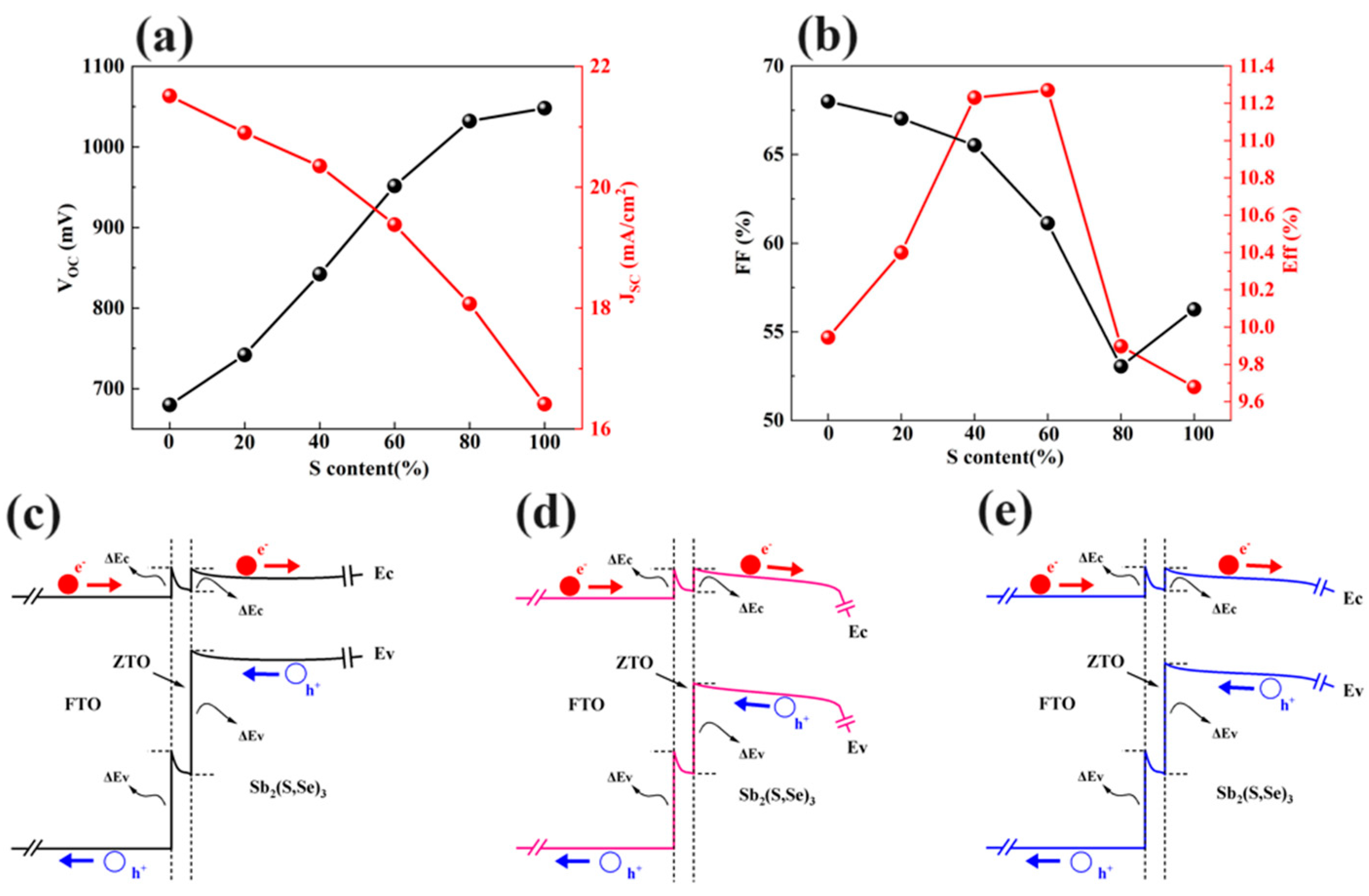
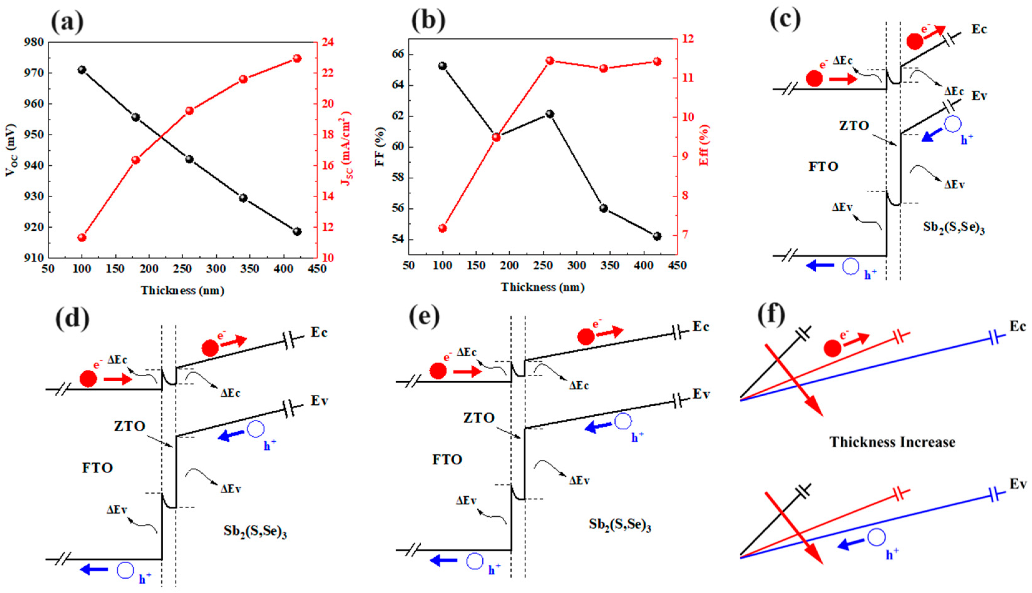
3.2.1. Effect of S Content and Thickness in Absorber Layer

To further investigate carrier collection at the ZTO/Sb2(S,Se)3 interface, the effect of S content in the absorber layer on the photovoltaic performance of the device was studied. Figure 6 illustrates the results of this investigation. As the S content in the absorber layer increases, the VOC of the device rises from 0.680 to 1.048 V. However, the JSC of the device decreases from 21.51 to 16.41 mA/cm2 with increasing S content, as shown in Figure 6a. Additionally, the FF of the device decreases from 68% to 56.26% as the S content increases from 0% to 100% in Figure 6b. Overall, the efficiency of the Sb2(S,Se)3 device increases with the S content up to 60%, after which it starts to decrease. The energy band diagrams of FTO/ZTO/Sb2(S,Se)3 with varying S content (0%, 60%, and 100%) are shown in Figure 6c–e. The VBO between the ZTO layer and Sb2(S,Se)3 layer decreases as the S content increases up to 60%. This lower VBO value indicates a reduced hole barrier at the ZTO/Sb2(S,Se)3 interface, facilitating the flow of photo-generated holes from the Sb2(S,Se)3 layer to the ZTO layer and reducing minority carrier recombination at the interface of the ZTO/Sb2(S,Se)3 heterojunction. Conversely, a higher S content leads to a higher VBO value at the ZTO/Sb2(S,Se)3 interface, indicating greater difficulty in transporting photo-generated holes from the Sb2(S,Se)3 absorber to the ZTO layer and resulting in increased carrier recombination. Based on these results, it is recommended that the Sb2(S,Se)3 absorber layer contain around 60% S content to achieve optimal photovoltaic properties in devices.
Figure 7 displays the effect of Sb2(S,Se)3 thickness on the photovoltaic parameters of the device. Increasing the thickness of Sb2(S,Se)3 from 100 nm to 420 nm results in a decrease in VOC from 0.971 V to 0.919 V, while JSC increases from 11.33 mA/cm2 to 22.96 mA/cm2 (Figure 7a). The FF initially decreases from 65.25% to 60.65% as the thickness goes from 100 nm to 180 nm but then slightly increases with further increase in thickness. In Figure 7b, the FF decreases from 62.14% to 54.2% as the thickness increases from 260 nm to 420 nm. Overall, the efficiency of the Sb2(S,Se)3 devices increases from 7.18% to 11.45% as the absorber layer thickness ranges from 100 nm to 260 nm. Further increases in thickness have a minimal impact on device efficiency. The energy band diagrams of FTO/ZTO/Sb2(S,Se)3 with various thicknesses of 100 nm, 260 nm, and 420 nm are illustrated in Figure 7c–e. The built-in potential barrier in the Sb2(S,Se)3 layer decreases as the absorber layer’s thickness increases from 100 nm to 260 nm (Figure 7f). This lower built-in potential barrier improves the transport of photo-generated electrons from the ZTO/Sb2(S,Se)3 interface to the Sb2(S,Se)3 layer, as well as the collection of photo-generated holes from the Sb2(S,Se)3 layer to the ZTO/Sb2(S,Se)3 interface. A thickness of 260 nm results in reduced carrier recombination in the Sb2(S,Se)3 layer and enhances the device’s efficiency. With further increases in thickness, the reduction in the built-in potential barrier in Sb2(S,Se)3 becomes slower, potentially leading to similar transport of photo-generated carriers in the Sb2(S,Se)3 layers with various thicknesses of 260 nm and 420 nm. Consequently, the efficiency of the device remains relatively constant with increasing thickness. The optimal thickness of Sb2(S,Se)3 is 260 nm in the device.

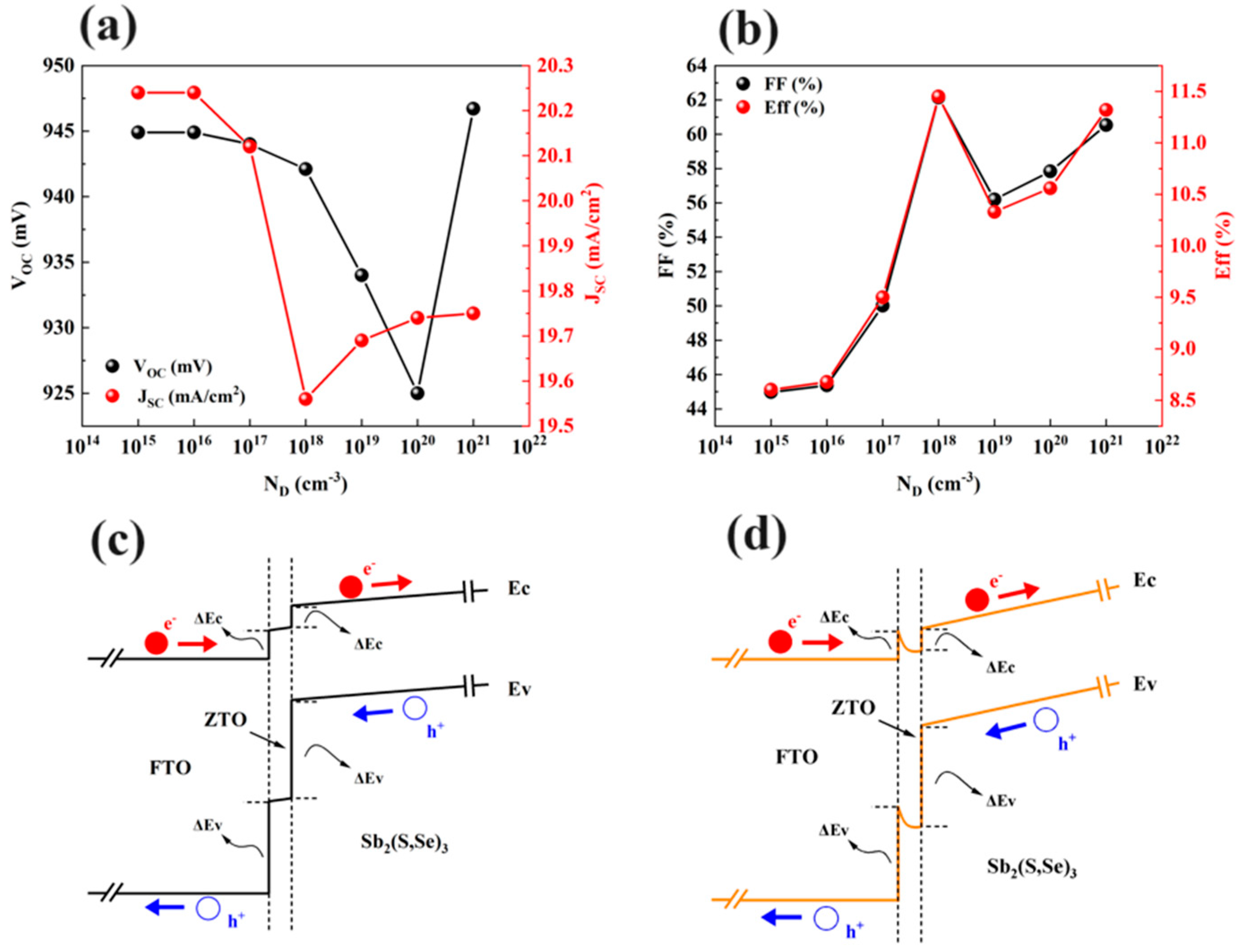
3.2.2. Impact of Carrier Concentration of ZTO Layer

Figure 8 displays the impact of the carrier concentration (ND) of the ZTO layer on the four parameters of the Sb2(S,Se)3 device. As the carrier concentration of the ZTO layer changes to 1 × 1020 cm−3, the VOC of the device is reduced from 0.945 V to 0.925 V. Further increasing the carrier concentration results in the VOC of the device changing from 0.925 V to 0.947 V. A study indicated that the enhanced built-in electric field at the interface between the ETL and absorber layer leads to an improvement in the VOC of the device [23]. A ZTO layer with a high carrier concentration of 1 × 1021 cm−3 can create an enhanced built-in electric field at the interface of the ZTO/Sb2(S,Se)3 heterojunction. This enhanced built-in electric field plays a crucial role in raising the device’s VOC from 0.925 V to 0.947 V. The JSC of the device varies from 20.24 mA/cm2 to 19.56 mA/cm2 as the carrier concentration of the ZTO layer changes from 1 × 1015 cm−3 to 1 × 1018 cm−3. JSC then increases as ND increases from 1 × 1018 cm−3 to 1 × 1021 cm−3. These numerical results are shown in Figure 8a. Figure 8b shows that the FF and PCE of the device increase as ZTO’s ND increases from 1 × 1015 cm−3 to 1 × 1018 cm−3. However, with a further increase in carrier concentration from 1 × 1018 cm−3 to 1 × 1019 cm−3, the FF and PCE decrease. Finally, as ND changes from 1 × 1019 cm−3 to 1 × 1021 cm−3, the FF and PCE of the device increase once again. Figure 8c,d illustrate the detailed energy band diagrams of FTO/ZTO/Sb2(S,Se)3. The CBO value and VBO value are 0.34 eV and 1.55 eV when the ND of ZTO is 1 × 1015 cm−3 in Figure 8c. A hole barrier can be seen at the interface between FTO and ZTO, hindering the collection of photo-generated holes from ZTO to the FTO layer. However, the CBO value and VBO value of the ZTO/Sb2(S,Se)3 interface stay at 0.34 eV and 1.55 eV in Figure 8d when the carrier concentration of ZTO further increases to 1 × 1018 cm−3. The disappearance of the hole barrier at the FTO/ZTO interface enhances the flow of photo-generated holes from ZTO to FTO, reducing the recombination of minority carriers and improving the FF of the Sb2(S,Se)3 device. Therefore, to achieve the best efficiency of the device, the ZTO layer should have an ND of 1 × 1018 cm−3.

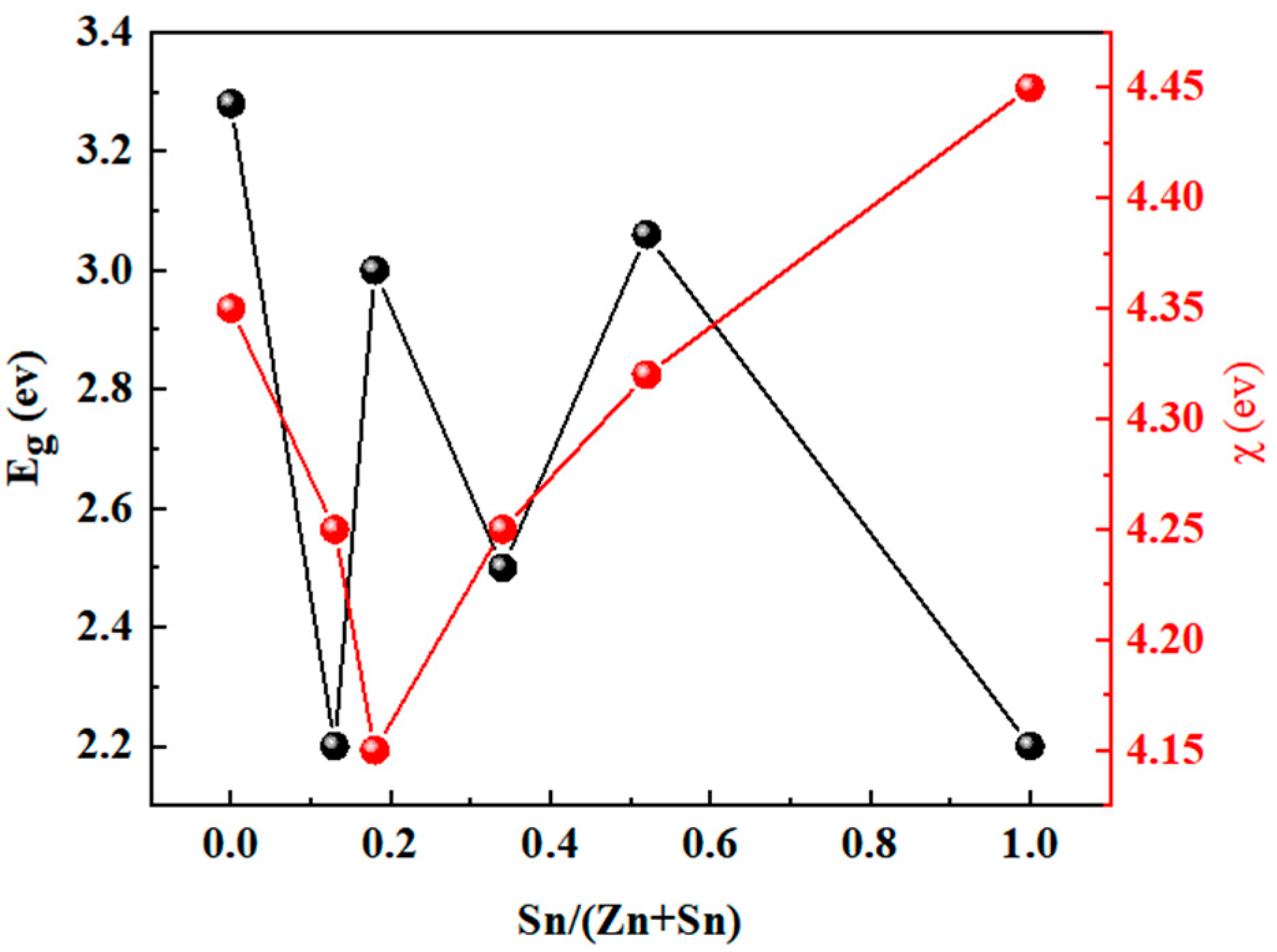
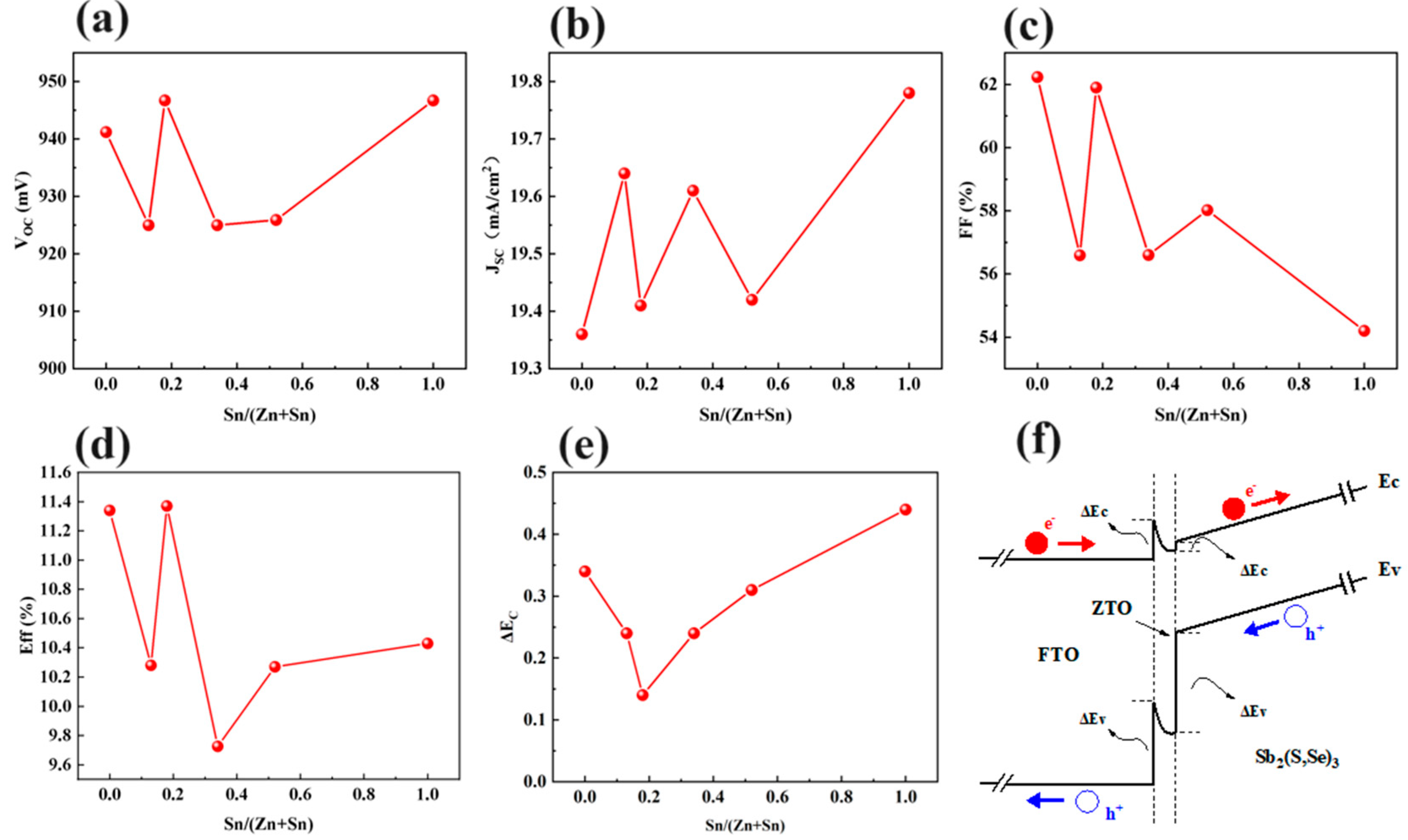
3.2.3. Effect of Sn/(Zn+Sn) Ratio in ZTO

In order to analyze the effect of the Sn/(Zn+Sn) ratio on the photo-generated minority carrier collection properties of Sb2(S,Se)3 devices, the Sn/(Zn+Sn) ratio in ZTO was varied from 0 to 1. In Figure 9a–d, the impact of the Sn/(Zn+Sn) ratio on the photovoltaic parameters of the device is illustrated. The optimal Sn/(Zn+Sn) ratio is found to be 0.18, resulting in the highest VOC for the device. Additionally, the optimal JSC of 19.76 mA/cm2 is achieved with a Sn/(Zn+Sn) ratio of 1.0. The effect of the Sn/(Zn+Sn) ratio on the FF of the devices is also studied, with the best FF obtained when the ZTO layer had a Sn/(Zn+Sn) ratio of 0.18. Furthermore, the PCE of the device is studied in relation to the Sn/(Zn+Sn) ratio. The best PCE is observed when the ZTO layer has a Sn/(Zn+Sn) ratio of 0.18. These results indicate that ZTO with a Sn/(Zn+Sn) ratio of 0.18 enhances the VOC, FF, and PCE of the device. To further investigate the impact of the Sn/(Zn+Sn) ratio on the minority carrier transport at the ZTO/Sb2(S,Se)3 interface, the simulation results are analyzed in Figure 9e,f. The effect of different Sn/(Zn+Sn) ratios on the CBO value at the interface of ZTO/Sb2(S,Se)3 is shown in Figure 9e. It is observed that the CBO value decreases from 0.34 eV to 0.13 eV as the Sn/(Zn+Sn) ratio increases from 0 to 0.18. Subsequently, the CBO value is enhanced from 0.13 eV to 0.43 eV as the Sn/(Zn+Sn) ratio increases from 0.18 to 1. The energy band diagram of FTO/ZTO (with a Sn/(Zn+Sn) ratio of 0.18)/Sb2(S,Se)3 is shown in Figure 9f. This ratio results in a lower conduction band offset (CBO) value at the interface between ZTO and Sb2(S,Se)3. Previous research has shown that a lower CBO value at the interface between the electron transport layer and the absorber layer can reduce interface recombination and the open-circuit voltage deficit and ultimately improve the efficiency of devices [24]. Therefore, the decreased CBO at the ZTO/Sb2(S,Se)3 interface enhances the VOC and efficiency of the Sb2(S,Se)3 device.

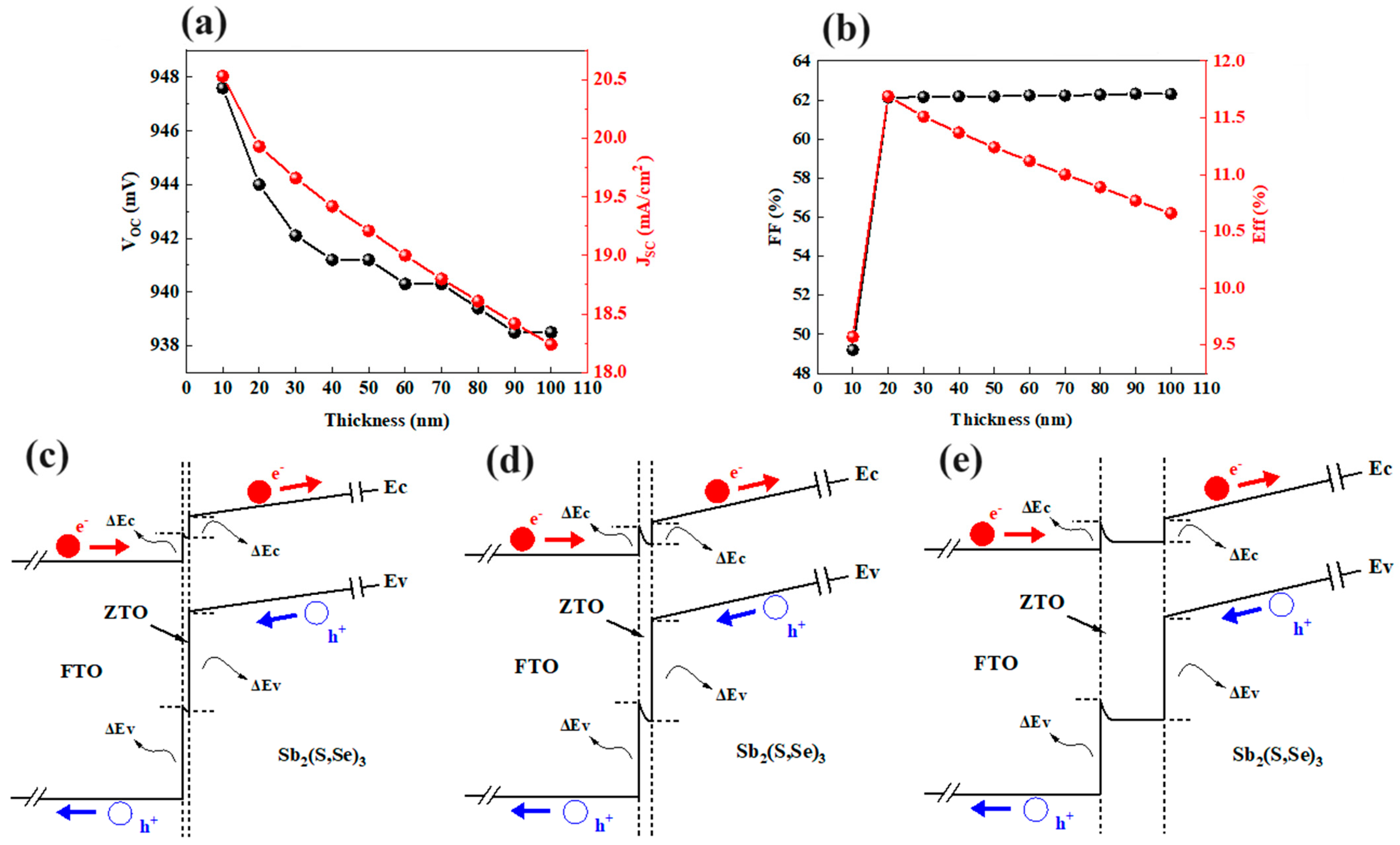
3.2.4. Effect of ZTO Thickness

We investigate the effect of ZTO thickness on the photovoltaic parameters of the device in Figure 10. The dependence of VOC on the ZTO thickness is illustrated in Figure 10a. It is observed that the VOC of the device generally decreases as the ZTO thickness increases from 10 nm to 100 nm. Similarly, JSC decreases as the ZTO thickness increases. Figure 10b depicts the effect of ZTO thickness on the FF and efficiency of the device. The FF increases with the thickness of the ZTO layer up to 20 nm but then plateaus with further increases in thickness. The efficiency of the device increases with the ZTO thickness up to 20 nm but then decreases with further increases in thickness. These results reveal that the optimal ZTO thickness is 20 nm. Figure 10c–e display the energy band diagrams of FTO/ZTO/Sb2(S,Se)3 structures with various ZTO thicknesses. The CBO and VBO values at the interface of the ZTO/Sb2(S,Se)3 heterojunction stay at 0.34 eV and 1.55 eV as the thickness of ZTO increases. The built-in electric field from ZTO to FTO can be seen at the FTO/ZTO interface. An enhanced built-in electric field is observed at the FTO/ZTO interface with increasing ZTO thickness up to 20 nm, facilitating the flow of photo-generated holes from the ZTO layer to the FTO layer. This reduction in carrier recombination in the ZTO layer is essential for improving efficiency. However, when the ZTO thickness reaches 100 nm, a flat band is seen at the CBM and VBM, which hinders the carrier flow and leads to increased carrier recombination in the ZTO layer, ultimately limiting the device’s efficiency. In conclusion, a ZTO thickness of 20 nm is optimal for achieving the highest efficiency of the device.

4. Conclusions

This study presents a theoretical simulation comparing the use of ZTO and CdS as ETLs in Sb2(S,Se)3 devices. The results show that the CBO at the ZTO/Sb2(S,Se)3 interface is cliff-like but has a lower value of 0.34 eV compared to the interface of CdS/Sb2(S,Se)3. The lower CBO value limits the recombination of minority carriers at the interface of ZTO/Sb2(S,Se)3. Additionally, the VBO value at the interface of ZTO/Sb2(S,Se)3 is higher than that at the CdS/Sb2(S,Se)3 interface. These improved CBO and VBO values at the ZTO/Sb2(S,Se)3 interface enhance the transport of carriers, resulting in an increase in the PCE of the devices from 7.56% to 11.45%. The presence of 60% S content in the Sb2(S,Se)3 layer constructs a low hole barrier at the interface of the ZTO/Sb2(S,Se)3 heterojunction, reducing photo-generated hole losses at the interface and leading to improved photovoltaic performance. The absorber with a thickness of 260 nm has a lower built-in potential barrier, reducing the carrier recombination in the Sb2(S,Se)3 absorber and improving the efficiency of the device. Furthermore, the hole barrier disappears at the interface of FTO/ZTO when the ZTO layer has a carrier concentration of 1 × 1018 cm−3, promoting the PCE of the devices. A Sn/(Zn+Sn) ratio of 0.18 in the ZTO layer optimizes the CBO value at the ZTO/Sb2(S,Se)3 interface, reducing carrier recombination at the interface. Moreover, a ZTO layer with a thickness of 20 nm produces an enhanced built-in electric field at the FTO/ZTO interface, further optimizing the efficiency of the devices.

Author Contributions

J.L.: writing—original draft, data curation, and conceptualization. Z.X.: methodology, investigation, and data curation. Y.G.: methodology, investigation, and software. C.C.: formal analysis and methodology. X.Z.: funding acquisition and investigation. X.C.: funding acquisition, methodology, software. J.H.: funding acquisition, writing—review and editing, and investigation. G.L.: supervision, formal analysis, and conceptualization. All authors have read and agreed to the published version of the manuscript.

Funding

This work was supported by the Science and Technology Plan Project of Shenzhen (20231122102326002), China, and the Songshan Lake Science and Technology Correspondent Project (2023080815295178), China.

Institutional Review Board Statement

Not applicable.

Informed Consent Statement

Not applicable.

Data Availability Statement

The raw data supporting the conclusions of this article will be made available by the authors on request.

Conflicts of Interest

The authors declare no conflicts of interest.

References

  1. Liang, G.X.; Li, C.H.; Zhao, J.; Fu, Y.; Yu, Z.X.; Zheng, Z.H.; Su, Z.H.; Fan, P.; Zhang, X.H.; Luo, J.T.; et al. Self-powered broadband kesterite photodetector with ultrahigh specific detectivity for weak light applications. SusMat 2023, 3, 682–696. [Google Scholar] [CrossRef]
  2. Lei, H.; Chen, J.; Tan, Z.; Fang, G. Review of recent progress in antimony chalcogenide-based solar cells: Materials and devices. Sol. RRL 2019, 3, 1900026. [Google Scholar] [CrossRef]
  3. Wang, X.; Tang, R.; Wu, C.; Zhu, C.; Chen, T. Development of antimony sulfide-selenide Sb2(S,Se)3-based solar cells. J. Energy Chem. 2018, 27, 713–721. [Google Scholar] [CrossRef]
  4. Jiang, C.; Zhou, J.; Tang, R.; Lian, W.; Wang, X.; Lei, X.; Zeng, H.; Zhu, C.; Tang, W.; Chen, T. 9.7%-efficient Sb2(S,Se)3 solar cells with a dithieno[3,2-b:2’,3’-d] pyrrolecored hole transporting material. Energy Environ. Sci. 2021, 14, 359–364. [Google Scholar] [CrossRef]
  5. Yang, B.; Qin, S.K.; Xue, D.J.; Chen, C.; He, Y.S.; Niu, D.M.; Huang, H.; Tang, J. In situ sulfurization to generate Sb2(Se1−xSx)3 alloyed films and their application for photovoltaics. Prog. Photovolt. 2017, 25, 113–122. [Google Scholar] [CrossRef]
  6. Pan, Y.L.; Hu, X.B.; Guo, Y.X.; Pan, X.Y.; Zhao, F.; Weng, G.E.; Tao, J.H.; Zhao, C.H.; Jiang, J.C.; Chen, S.Q.; et al. Vapor transport deposition of highly efficient Sb2(S,Se)3 solar cells via controllable orientation growth. Adv. Funct. Mater. 2012, 31, 2101476. [Google Scholar] [CrossRef]
  7. Chen, C.; Yin, Y.W.; Lian, W.T.; Jiang, L.F.; Tang, R.F.; Jiang, C.H.; Wu, C.Y.; Gao, D.; Wang, X.M.; Fang, F.; et al. Pulsed laser deposition of antimony selenosulfide thin film for the efficient solar cells. Appl. Phys. Lett. 2020, 116, 133901. [Google Scholar] [CrossRef]
  8. Wu, C.Y.; Lian, W.T.; Zhang, L.J.; Ding, H.H.; Jiang, C.H.; Ma, Y.Y.; Han, W.H.; Li, Y.M.; Zhu, J.F.; Chen, T.; et al. Water additive enhanced solution processing of alloy Sb2(S1−xSex)3-based solar cells. Sol. RRL 2020, 4, 1900582. [Google Scholar] [CrossRef]
  9. Wang, X.M.; Tang, R.F.; Jiang, C.H.; Lian, W.T.; Ju, H.X.; Jiang, G.S.; Li, Z.Q.; Zhu, C.F.; Chen, T. Manipulating the electrical properties of Sb2(S,Se)3 film for high-efficiency solar cell. Adv. Energy Mater. 2020, 10, 2002341. [Google Scholar] [CrossRef]
  10. Li, S.; Lu, S.C.; Lu, Y.; Xue, J.Y.; Li, K.H.; Chen, C.; Tang, J. Efficient Sb2(S,Se)3 solar cells via monitorable chemical bath deposition. J. Mater. Chem. A 2022, 10, 11625–11635. [Google Scholar] [CrossRef]
  11. Zhao, Y.Q.; Wang, S.Y.; Jiang, C.H.; Li, C.; Xiao, P.; Tang, R.F.; Gong, J.B.; Chen, G.L.; Chen, T.; Li, J.M.; et al. Regulating energy band alignment via alkaline metal fluoride assisted solution post-treatment enabling Sb2(S,Se)3 solar cells with 10.7% efficiency. Adv. Energy Mater. 2021, 12, 2103015. [Google Scholar] [CrossRef]
  12. Huang, M.L.; Xu, P.; Han, D.; Tang, J.; Chen, S.Y. Complicated and unconventional defect properties of the quasi-one-dimensional photovoltaic semiconductor Sb2Se3. ACS Appl. Mater. Interfaces 2019, 11, 15564–15572. [Google Scholar] [CrossRef] [PubMed]
  13. Liu, X.S.; Chen, J.; Luo, M.; Leng, M.Y.; Xia, Z.; Zhou, Y.; Qin, S.K.; Xue, D.J.; Lv, L.; Huang, H.; et al. Thermal evaporation and characterization of Sb2Se3 thin film for substrate Sb2Se3/CdS solar cells. ACS Appl. Mater. Interfaces 2014, 6, 10687–10695. [Google Scholar] [CrossRef] [PubMed]
  14. Huang, L.K.; Sun, X.X.; Li, C.; Xu, R.; Xu, J.; Du, Y.Y.; Wu, Y.X.; Ni, J.; Cai, H.K.; Li, J.; et al. Electron transport layer-free planar perovskite solar cells: Further performance enhancement perspective from device simulation. Sol. Energy Mater. Sol. Cells 2016, 157, 1038–1047. [Google Scholar] [CrossRef]
  15. Dabbabi, S.; Nasr, T.B.; Kamoun-Turki, N. Parameters optimization of CIGS solar cell using 2D physical modeling. Results Phys. 2017, 7, 4020–4024. [Google Scholar] [CrossRef]
  16. Gobbo, C.; Di Palma, V.; Trifiletti, V.; Malerba, C.; Valentini, M.; Matacena, L.; Daliento, S.; Binetti, S.; Acciarri, M.; Tseberlidis, G. Effect of the ZnSnO/AZO interface on the charge extraction in Cd-free kesterite solar cells. Energies 2023, 16, 4137. [Google Scholar] [CrossRef]
  17. Anwar, F.; Mahbub, R.; Satter, S.S.; Ullah, S.M. Effect of different HTM layers and electrical parameters on ZnO nanorod-based lead-free perovskite solar cell for high-efficiency performance. Int. J. Photoenergy 2017, 2017, 9846310. [Google Scholar] [CrossRef]
  18. Azri, F.; Meftah, A.; Sengouga, N.; Meftah, A. Electron and hole transport layers optimization by numerical simulation of a perovskite solar cell. Sol. Energy 2019, 181, 372–378. [Google Scholar] [CrossRef]
  19. Nicolas-Marin, M.M.; Ayala-Mato, F.; Vigil-Galan, O.; Courel, M. Simulation analysis of Cd1−xZnXS/Sb2(Se1−xSX)3 solar cells with n-i-p structure. Sol. Energy 2021, 224, 245–252. [Google Scholar] [CrossRef]
  20. Saadat, M.; Amiri, O. Fine adjusting of charge carriers transport in absorber/HTL interface in Sb2(S,Se)3 solar cells. Sol. Energy 2022, 243, 163–173. [Google Scholar] [CrossRef]
  21. Jimenez, T.; Seuret-Jimenez, D.; Vigil-Galan, O.; Basurto-Pensado, M.A.; Courel, M. Sb2(S1−xSeX)3 solar cells: The impact of radiative and non-radiative loss mechanisms. J. Phys. D Appl. Phys. 2018, 51, 435501. [Google Scholar] [CrossRef]
  22. Lee, S.; Kim, S.; Shin, S.; Jin, Z.; Min, Y.S. Band structure of amorphous zinc tin oxide thin films deposited by atomic layer deposition. J. Ind. Eng. Chem. 2018, 58, 328–333. [Google Scholar] [CrossRef]
  23. Shaker, A.; Salem, M.S.; Jayan, K.D. Analysis and design of p-n homojunction Sb2Se3 solar cells by numerical simulation. Sol. Energy 2022, 242, 276–286. [Google Scholar] [CrossRef]
  24. Wang, W.H.; Yao, L.Q.; Dong, J.B.; Wu, L.; Cao, Z.X.; Hui, L.; Chen, G.L.; Luo, J.S.; Zhang, Y. Interface modification uncovers the potential application of SnO2/TiO2 double electron transport layer in efficient cadmium-free Sb2Se3 devices. Adv. Mater. Interfaces 2022, 9, 2102464. [Google Scholar] [CrossRef]
Figure 1. The two structures investigated in this work: (a) an Sb2(S,Se)3 device with a CdS layer and (b) an Sb2(S,Se)3 device with a Zn1−xSnxOy layer.
Materials 17 03214 g001
Figure 2. The relationship between the band gap of Sb2(S,Se)3 and the S content of Sb2(S,Se)3.
Materials 17 03214 g002
Figure 3. The relationship between the band gap of the ZTO layer, the electron affinity of the ZTO layer, and the Sn/(Zn+Sn) ratio.
Materials 17 03214 g003
Figure 4. Calculated (a) VOC and JSC and (b) FF and efficiency for Sb2(S,Se)3 devices as a function of the thickness of Sb2(S,Se)3.
Materials 17 03214 g004
Figure 5. (a) The band gap and electron affinity of each layer in Sb2(S,Se)3 devices, (b) J-V curves of Sb2(S,Se)3 devices with CdS and ZTO ETLs, and the energy band diagrams of Sb2(S,Se)3 devices with (c) CdS and (d) ZTO layers.
Materials 17 03214 g005
Figure 6. Changes in (a) VOC and JSC and (b) FF and efficiency for different S contents in Sb2(S,Se)3, and the energy band diagrams of FTO/ZTO/Sb2(S,Se)3 structures with (c) 0% S content in the absorber, (d) 60% S content in the absorber, and (e) 100% S content in the absorber.
Materials 17 03214 g006
Figure 7. Changes in (a) VOC and JSC and (b) FF and efficiency for various thicknesses in Sb2(S,Se)3; the energy band diagrams of FTO/ZTO/Sb2(S,Se)3 structures with absorber thicknesses of (c) 100nm, (d) 260 nm, and (e) 420 nm; and (f) the effect of the absorber thickness on the built-in potential barrier in the Sb2(S,Se)3 layer.
Materials 17 03214 g007
Figure 8. Calculated (a) VOC and JSC and (b) FF and efficiency for Sb2(S,Se)3 devices as a function of the carrier concentration of ZTO, and the energy band diagrams of FTO/ZTO/Sb2(S,Se)3 structures when ZTO’s carrier concentration is (c) 1 × 1015 cm−3 and (d) 1 × 1018 cm−3.
Materials 17 03214 g008
Figure 9. The calculated (a) VOC, (b) JSC, (c) FF, and (d) efficiency of the Sb2(S,Se)3 device as a function of the Sn/(Zn+Sn) ratio of ZTO, (e) the effect of the Sn/(Zn+Sn) ratio of ZTO on the conduction band offset (CBO), and (f) the energy band diagram of the FTO/ZTO/Sb2(S,Se)3 structure (the Sn/(Zn+Sn) ratio of ZTO is 0.18).
Materials 17 03214 g009
Figure 10. Changes in (a) VOC and JSC and (b) FF and efficiency for different thicknesses of the ZTO layer, and the energy band diagrams of FTO/ZTO/Sb2(S,Se)3 structures with ZTO thicknesses of (c) 10 nm, (d) 20 nm, and (e) 100 nm.
Materials 17 03214 g010
Table 1. Simulated parameters of the solar cells.
ParametersFTOSb2(S,Se)3Spiro-oMeTADCdSZTO
Thickness (nm)230260906234
εr914.383109
χ (eV)4.84.0124.54.35
Eg (eV)3.71.4932.42.7
NC (cm−3)2.2 × 10182.2 × 10182.5 × 10182.2 × 10182.2 × 1018
NV (cm−3)1.8 × 10191.8 × 10201.8 × 10191.8 × 10191.8 × 1019
µe (cm2/V.s)20141.0 × 10−410030
µh (cm2/V.s)102.62.0 × 10−4255
NA (cm−3)1.0 × 10145.0 × 101810
ND (cm−3)1.0 × 10204.0 × 10171015–1021
Vth,e (cm/s)1.0 × 1071.0 × 1071.0 × 10181.0 × 1071.0 × 107
Vth,p (cm/s)1.0 × 1071.0 × 1071.0 × 10181.0 × 1071.0 × 107
Table 2. Bulk defect parameters of the solar cells.
FTOSb2(S,Se)3Spiro-oMeTADCdSZTO
Defect 1Defect 2
Defect TypeSingle AcceptorSingle AcceptorSingle AcceptorSingle AcceptorSingle DonorSingle Neutral
Nt1.0 × 10151.3 × 10141.0 × 10151.0 × 10181.0 × 10143.0 × 1017
σe(cm2)1.0 × 10−151.99 × 10−141.99 × 10−141.0 × 10−153.0 × 10−151.0 × 10⁻¹⁴
σh(cm2)1.0 × 10−151.99 × 10−141.99 × 10−141.0 × 10−152.0 × 10−141.0 × 10⁻¹⁵
Disclaimer/Publisher’s Note: The statements, opinions and data contained in all publications are solely those of the individual author(s) and contributor(s) and not of MDPI and/or the editor(s). MDPI and/or the editor(s) disclaim responsibility for any injury to people or property resulting from any ideas, methods, instructions or products referred to in the content.

