Article

High Electron Mobility in Si-Doped Two-Dimensional β-Ga2O3 Tuned Using Biaxial Strain

1
College of Science, Hunan University of Science and Engineering, Yongzhou 425199, China
2
College of Materials Science and Engineering, Hunan University, Changsha 410082, China
3
Fujian Provincial Key Laboratory of Semiconductors and Applications, Collaborative Innovation Center for Optoelectronic Semiconductors and Efficient Devices, Department of Physics, Xiamen University, Xiamen 361005, China
*
Authors to whom correspondence should be addressed.
Materials 2024, 17(16), 4008; https://doi.org/10.3390/ma17164008
Submission received: 29 June 2024 / Revised: 3 August 2024 / Accepted: 5 August 2024 / Published: 12 August 2024

Abstract

:
Two-dimensional (2D) semiconductors have attracted much attention regarding their use in flexible electronic and optoelectronic devices, but the inherent poor electron mobility in conventional 2D materials severely restricts their applications. Using first-principles calculations in conjunction with Boltzmann transport theory, we systematically investigated the Si-doped 2D β-Ga2O3 structure mediated by biaxial strain, where the structural stabilities were determined by formation energy, phonon spectrum, and ab initio molecular dynamic simulation. Initially, the band gap values of Si-doped 2D β-Ga2O3 increased slightly, followed by a rapid decrease from 2.46 eV to 1.38 eV accompanied by strain modulations from −8% compressive to +8% tensile, which can be ascribed to the bigger energy elevation of the σ* anti-bonding in the conduction band minimum than that of the π bonding in the valence band maximum. Additionally, band structure calculations resolved a direct-to-indirect transition under the tensile strains. Furthermore, a significantly high electron mobility up to 4911.18 cm2 V−1 s−1 was discovered in Si-doped 2D β-Ga2O3 as the biaxial tensile strain approached 8%, which originated mainly from the decreased quantum confinement effect on the surface. The electrical conductivity was elevated with the increase in tensile strain and the enhancement of temperature from 300 K to 800 K. Our studies demonstrate the tunable electron mobilities and band structures of Si-doped 2D β-Ga2O3 using biaxial strain and shed light on its great potential in nanoscale electronics.

1. Introduction

Bulk β-gallium oxide (β-Ga2O3) possesses an ultrawide band gap (4.8 eV); however, its low mobility significantly limits its applications [1,2,3]. Doping engineering is one effective method that is used to tune the conductivity of wide-band gap semiconductors such as β-Ga2O3 [4,5,6,7,8]. Among plentiful dopants, the Si dopant is peculiar since it is not only one of the unintentionally introduced impurities during synthesis and device fabrication but also plays a vital role in modifying electron mobility, as reported in three-dimensional (3D) β-Ga2O3 [9]. For Si-doped 3D β-Ga2O3, electron mobilities of 0.1–196 cm2 V−1 s−1 have been reported. Baldini et al. studied the electron mobility of Si-doped homoepitaxial β-Ga2O3 films ranging from ~50 cm2 V−1 s−1 for a doping concentration of n = 8 × 1019 cm−3 to ~130 cm2 V−1 s−1 for a doping concentration of n = 1 × 1017 cm−3 [10]. Hernandez et al. illustrated that Si-doped homoepitaxial β-Ga2O3 films grown by chemical vapor deposition were characterized by electron mobilities in the range of 0.59–30.59 cm2 V−1 s−1 for Si concentrations ranging from 89.2 to 17.8 nmol/min [11]. Recently, Bhattacharyya et al. reported an electron mobility of 196 cm2 V−1 s−1 (n = 2.3 × 1016 cm−3) measured in a Si-doped β-Ga2O3 film grown on Fe-doped β-Ga2O3 substrates at 810 °C, which is the highest electron mobility value ever reported in β-Ga2O3 epitaxial films, suggesting the great potential of Si dopants in tuning the electron mobility of 3D β-Ga2O3 [12]. For these reported heteroepitaxial films, Zhang et al. indicated that the electron mobility was 0.1, 0.1, 0.5, and 5.5 cm2 V−1 s−1 for 0, 1.1, 4.1, and 10.4% Si-doped β-Ga2O3 thin films on sapphire substrates prepared using pulsed laser deposition (PLD) at 500 °C, respectively [13]. Khartsev et al. prepared high-quality Si-doped β-Ga2O3 films on sapphire substrates using PLD and reported an electron mobility of about 2.9 cm2 V−1 s−1 for n = 2.5 × 1019 cm−3 [14]. Wong et al. reported electron mobilities of 90–100 cm2 V−1 s−1 at carrier concentrations in the low to mid 1017 cm−3 range in β-Ga2O3 (010) using Si-ion implantation doping and molecular beam epitaxy [15].
Two-dimensional (2D) semiconductors have attracted much attention and are widely used in electronic and optoelectronic devices [16,17,18,19,20,21,22]. In the past few years, research interest has been mostly focused on graphene [23], transition metal dichalcogenides (TMDs) [24], and other materials in order to design new nanoelectronic devices, including solar cells and field effect transistors. Although the 2D materials mentioned above usually possess outstanding properties, some of their disadvantages, such as the zero band gap of graphene and the low carrier mobilities of TMDs, make it temporarily difficult to adopt multifunctional applications. Therefore, the discovery and engineering of novel 2D materials with moderate band gaps and high carrier mobility are worthy of research focus. Lately, the fabrication of 2D β-Ga2O3 was reported using mechanical exfoliation, molecular beam epitaxy, and chemical synthesis methods, and its benefits stemmed from its fragile Ga-O bonds along the β-Ga2O3 [100] direction [25,26]. Owing to its lower-dimensional nature and its high surface-to-volume ratio, 2D β-Ga2O3 exhibits better physical properties and enormous potential for novel applications. For instance, a monolayer of β-Ga2O3 passivated by H possessed electron mobilities as high as 2685 cm2 V−1 s−1 and 156 cm2 V−1 s−1 along the b and c directions, respectively, based on theoretical studies [27]. The features of 2D β-Ga2O3-based solar-blind photodetectors were boosted to nearly three times higher than that of bulk β-Ga2O3 [28,29,30]. Therefore, 2D β-Ga2O3 has great potential for innovative nanoscale applications because it combines the benefits of outstanding electron mobility with affordable production techniques.
However, both theoretical and experimental efforts devoted to modifying the carrier mobility in Si-doped 2D β-Ga2O3 materials are lacking. Only limited reports showed the preferred Si atom occupation of the tetrahedral Ga site, which resulted in donor doping behaviors in Si-doped 2D β-Ga2O3 [31]. Especially considering the different local crystal structures of 2D and 3D β-Ga2O3, the results presented regarding 3D β-Ga2O3 are difficult to directly apply to 2D systems, which motivated us to comprehensively analyze the effects of Si dopants on the electronic and transport properties of 2D β-Ga2O3 here. Additionally, previous work showed that the 2D β-Ga2O3 is characterized by low elastic constants; therefore, systematic strain-modulated band structure investigations of 2D β-Ga2O3 shed light on its potential for use in the fabrication of flexible electronic devices [32]. Inspired by these concepts, we carried out first-principles calculations using the Perdew–Burke–Ernzerhof (PBE) functional and the Boltzmann transport theory to explore the strain-modulated transport properties of Si-doped 2D β-Ga2O3. Our work demonstrates that the electron mobilities and band structures of Si-doped 2D β-Ga2O3 are tunable using biaxial strain, highlighting its great potential for use in nanoscale electronics.

2. Calculation Methods

2.1. Computational Details

Vienna ab initio Simulation Package (VASP) Standard Edition 6.4 was used for first-principles calculations [33,34]. The generalized gradient approximation (GGA) of the PBE functional was adopted [35,36]. In this study, a 3 × 2 × 1 2D β-Ga2O3 supercell including 60 atoms was modeled. The criteria of energy cutoff, energy convergence, and residual forces were 450 eV, 1 × 10⁻⁶ eV/atom, and 0.01 eV/Å, respectively. The k-point grid was set at a resolution of 0.02 × 2π Å−1. The vacuum thickness was set at 15 Å along the c-axis direction to prevent the spurious interactions between layers. Bulk β-Ga2O3 contains two different Ga coordinations, i.e., octahedral GaI and tetrahedral GaII. Along the β-Ga2O3 [100] direction, bulk β-Ga2O3 can be cleaved into 2D β-Ga2O3 with a low cleavage energy [37]. After cleaving from 3D β-Ga2O3, as shown in Figure 1a, the GaII maintained four coordinations, whereas the GaI changed from six coordinations in 3D β-Ga2O3 to five coordinations in 2D β-Ga2O3. Thus, one 2D β-Ga2O3 is endowed with two inequivalent Ga sites, namely the square pyramidal GaI and the tetrahedral GaII. The ionic radius of Si4+ (0.040 nm) dopant is slightly lower than that of host Ga3+ (0.062 nm), which makes it difficult to be in the interstitial position and easier to substitute Ga atoms. Therefore researchers have focused on its substitution style instead of interstitial doping in 3D and 2D β-Ga2O3 systems theoretically [31,38,39] and experimentally [12] in the literature. In this study, one Si impurity was substituted at the GaI and GaII cation sites labeled as SiGaI and SiGaII, respectively, as illustrated in Figure 1a. Furthermore, in this work, the x and y directions correspond to the crystalline a and b directions, respectively.
The dynamical stability was evaluated by phonon dispersion based on density functional perturbation theory (DFPT) within a 6 × 2 × 1 supercell [40]. The structural convergence criteria of energy and force were 10−8 eV and 10−7 eV/Å, respectively. To gain thermodynamical stability, ab initio molecular dynamic (AIMD) simulation was adopted within a 6 × 2 × 1 supercell. The electron mobility and relaxation time were determined by the deformation potential (DP) theory [41]. The Boltzmann theory with the BoltzTraP2 code was utilized to determine the electrical conductivity [42].

2.2. Formation Energies and Carrier Mobility Calculations

The formation energy E f of Si-doped 2D β-Ga2O3 is defined as [43,44]
E f = E d e f e c t E G a 2 O 3 i n i μ i
where E d e f e c t and E G a 2 O 3 , respectively, represent the energy of the Si-doped and pure 2D β-Ga2O3 configuration. n i demonstrates the quantity of i atom added ( n i < 0 ) or extracted ( n i > 0 ) from the pure β-Ga2O3 system. The chemical potential of μ Si and μ O is gained from the stable bulk Si and O2, respectively. The related chemical potential should meet the boundary conditions and fall into the O-rich and Ga-rich cases in terms of the growth conditions, as stated in our previous works [5,43].
Based on the DP theory, the carrier mobility μ is calculated as follows [45]:
μ = 2 e h 3 C 2 D ( 2 π ) 3 × 3 k B T | m * | 2 E 1 2
where kB, h, e, and T are the Boltzmann constant, Planck constant, electric charge, and the temperature (300 K), respectively. The electron mobility μ and relaxation time τ are determined by the deformation potential (DP) theory, where three inconstant parameters are necessary, i.e., the deformation potential constant E1, elastic stiffness C2D, and the electron effective mass me*. Deformation potential constant E1 is calculated by E 1 = E e d g e / ( Δ a / a 0 ) , which denotes the shift of the band edge accompanied by uniaxial strain. Here, E e d g e illustrates the shifted energy of the conduction band minimum (CBM), Δ a / a 0 is the variation in the lattice constant along a certain strained direction, and elastic stiffness C2D is calculated by C 2 D = [ 2 E / ( Δ a / a 0 ) 2 ] / S 0 . Here, E is the total energy of the strained optimized supercell, and S 0 is the surface area of the strained structure. The electron effective mass me* is calculated based on the equation as m e * = 2 / ( 2 E / k 2 ) by fitting the band curves close to the CBM, and k is the electron wave vector. The CBM and valence band maximum (VBM) values are obtained from the band structures of Si-doped 2D β-Ga2O3. The relaxation time is estimated by τ = μ m e * / e .

3. Results and Discussion

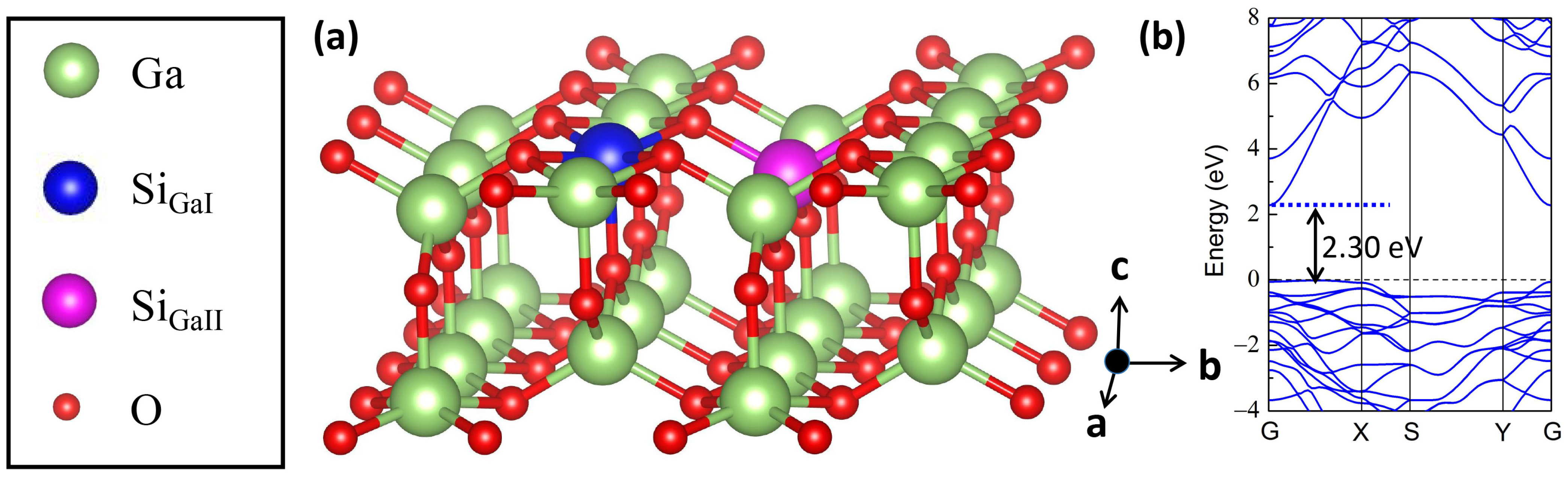
3.1. Structural Stability

Pure 2D β-Ga2O3 possesses the lattice constants of a = 2.97 Å, b = 5.74 Å, which are in accordance with those of previous works [46,47]. The calculated lattice constants for SiGaI and SiGaII structures are a = 2.98 Å, b = 5.77 Å and a = 2.99 Å, b = 5.76 Å, respectively. Only a slight structural difference was observed due to the small alteration in local structures and the similar ionic radii between the host Ga and the Si dopant. The formation energies for SiGaI and SiGaII structures are −5.41 and −6.27 eV, respectively, under O-rich conditions, which demonstrates that the Si dopant preferentially incorporates on the tetrahedrally coordinated GaII site. This is consistent with the result of Ref. [31]. Moreover, SiGaI and SiGaII structures possess the formation energies of −0.98 and −1.84 eV under a Ga-rich environment, respectively, illustrating that the foreign Si atom also prefers to occupy the GaII site herein. The higher formation energies also suggest the difficulty of introducing Si dopant in a Ga-rich atmosphere. In terms of the lower formation energy of the SiGaII configuration compared with that of SiGaI, we merely studied the SiGaII case under O-rich conditions afterwards. The phonon dispersion spectrum and AIMD simulation of the SiGaII structure are employed in Figure S1a,b (supporting materials), indicating the dynamical stability and thermodynamical stability of the SiGaII system, respectively.

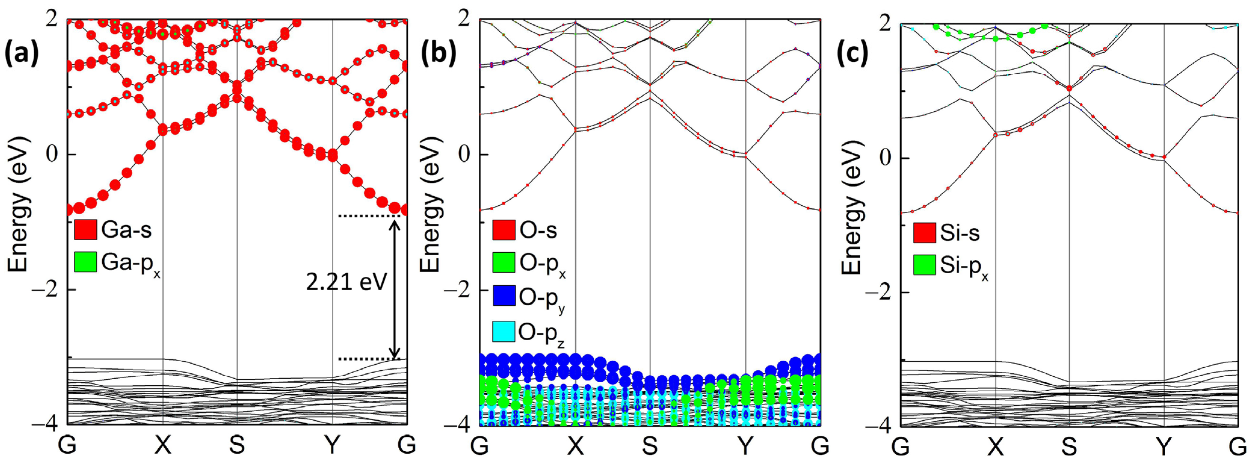
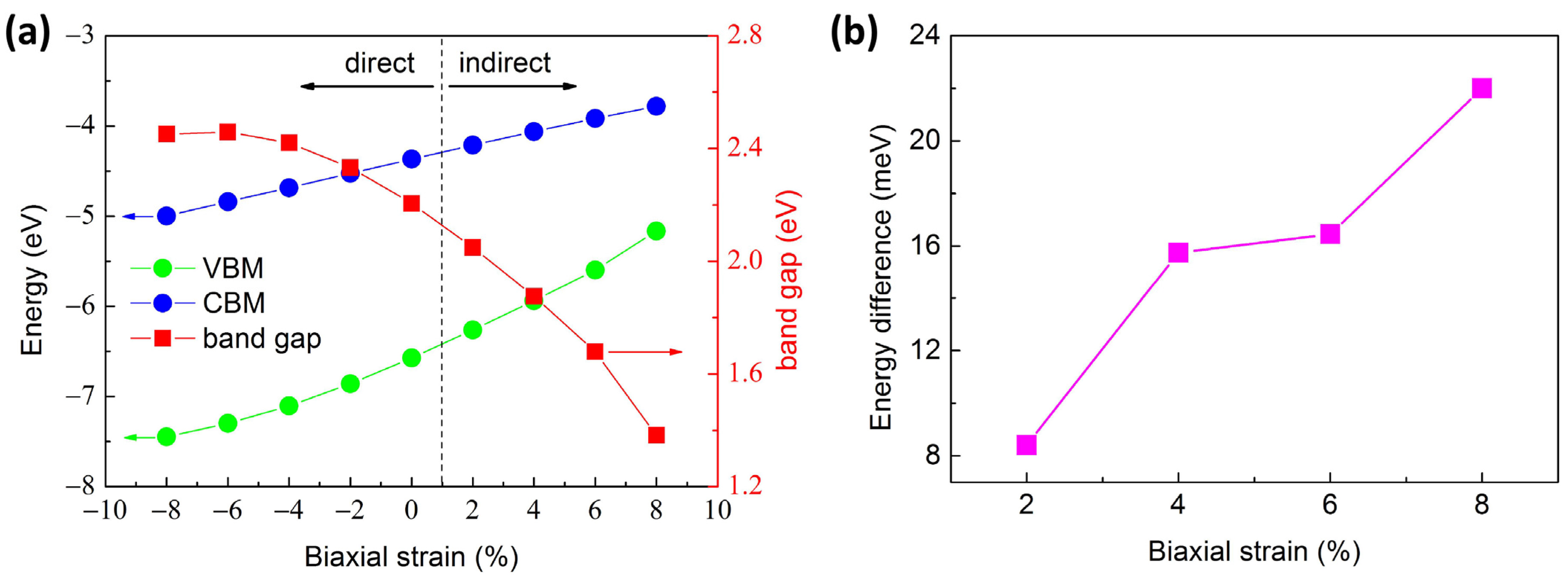
3.2. Strain-Engineered Band Structures

Figure 1b shows the band structure of perfect 2D β-Ga2O3, where the CBM is situated at the G point, whereas the VBM is positioned between the G and X points, demonstrating an indirect band gap semiconductor character. The calculated band gap of 2D β-Ga2O3 is 2.30 eV, which agrees well with previous works [45,47], but it is lower than the value of 3D β-Ga2O3 [48,49]. As shown in Figure 2, after substituting the tetrahedrally coordinated GaII with one Si atom, the band gap was slightly reduced to 2.21 eV. Moreover, the shift of VBM from the non-G point (between the G and X points) to the G point resulted in the direct band gap nature. These observations are consistent with the results in ref. [31]. Additionally, the orbital-projected band structures in Figure 2a–c illustrate that the majority of the VBM of SiGaI is composed of O-2p orbitals, whilst the CBM is mainly contributed by Ga-4s and small quantities of O-2s and Si-3s orbitals.
The variations in band edges relative to the vacuum level and the band gaps of SiGaII versus biaxial strain are shown in Figure 3a. The band gaps of SiGaII increased slightly at first followed by a rapid decrease when the strain was applied from −8% compressive to +8% tensile cases. We note that this strain interval is of research focus in 2D β-Ga2O3 systems theoretically, which can also be induced by the lattice mismatch, ideally using a different substrate. The orbital-projected band structures of SiGaII in Figure 2 can be used to explore the evolution behaviors of band gaps caused by biaxial strain. The σ* anti-bonding states that predominated in the CBM of SiGaII are formed by the exceptional Ga-s orbitals, tiny O-s, and Si-s orbitals; the π bonding states near VBM of SiGaII are mainly occupied by O-py orbitals. In general, lengthening the π bonding and σ* anti-bonding (from compressive to tensile strains) gives rise to the energy increases in CBM and VBM, as shown in Figure 3a [50]. The changes in energy levels can be attributed to the introduction of the Si dopant, whose orbital energy levels are hybridized with the host Ga-S orbitals, resulting in band gap changes. Consequently, the bigger the energy elevation of the VBM relative to the CBM, the smaller the band gap.
When applying biaxial tensile strain, the VBM moved from the G point to the non-G point, which resulted in a direct-to-indirect band gap transition. According to our findings, the location of VBM is therefore more susceptible to biaxial tensile strain than to biaxial compressive strain. Moreover, the compressive strain is beneficial for maintaining a direct band gap in the SiGaII structure. When biaxial strain was applied, the band gaps of SiGaII were tunable from 2.46 eV (−8% compressive strain) to 1.38 eV (+8% tensile strain). The energy differences between the direct and indirect band gap with respect to the biaxial tensile strains are shown in Figure 3b. One can notice that the energy difference was increased from 8 to 22 meV as the tensile strains increased.

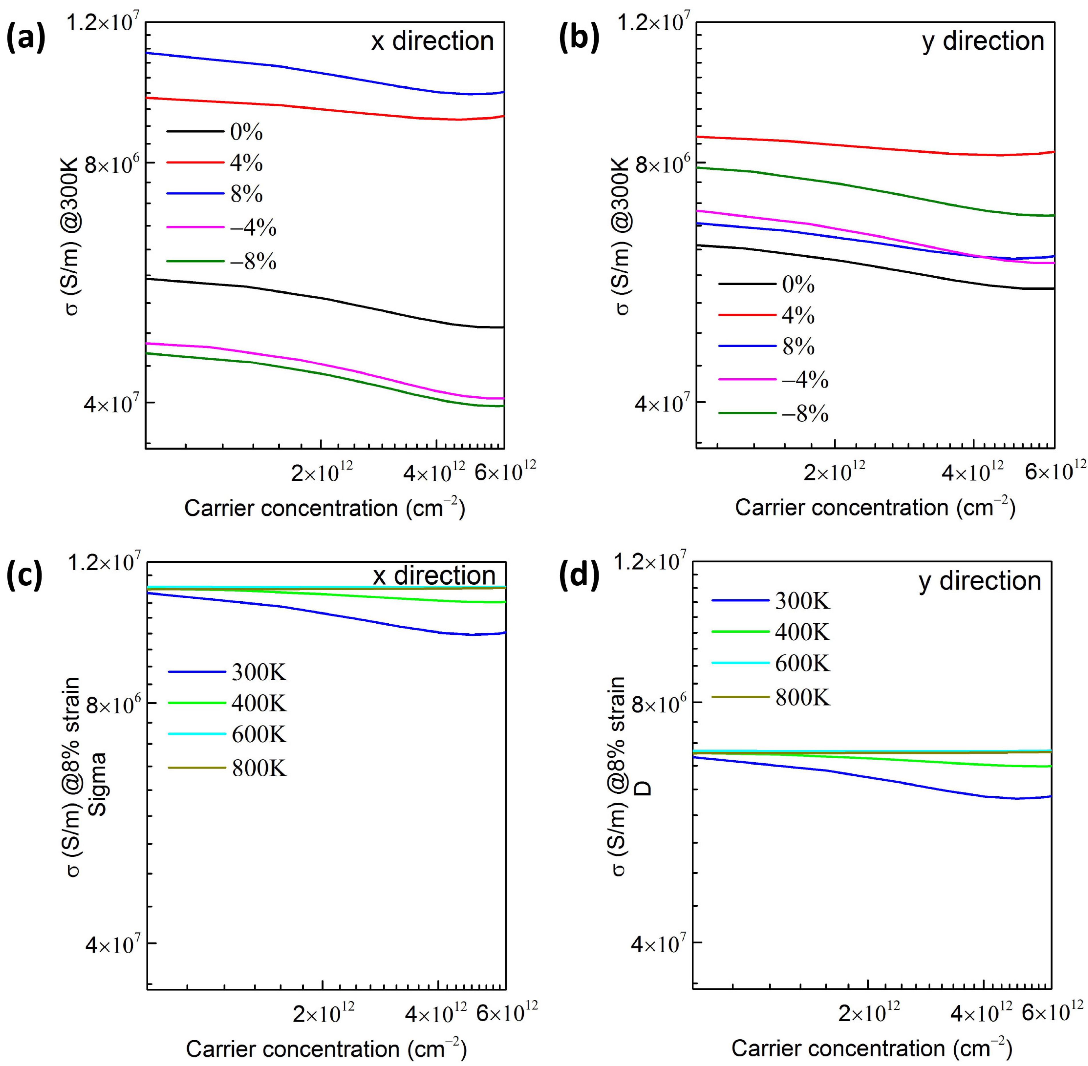
3.3. Strain-Engineered Transport Properties

The fluctuations of electronic structures with different strains were further employed to determine the carrier mobility (μ) and effective masses (m*). The electron effective masses (me*) along the G–X and G–Y directions are labeled mex* and mey*, respectively. The calculated mex* and mey* of perfect 2D β-Ga2O3 are 0.29 m0 and 0.27 m0, respectively, which is in good agreement with the results of 0.31 m0 and 0.29 m0 in Ref. [51], as well as 0.36 m0 and 0.36 m0 (isotropy) in Ref. [52]. For unstrained SiGaII, the calculated mex* and mey* are 0.30 m0 and 0.28 m0, respectively, as shown in Figure 4a. The detailed variations in mex* and mey* under biaxial strains are exhibited in Figure 4a. It can be shown that the mex* and mey* significantly decreased from biaxial compressive to tensile strains. The small me* generally implied a higher electron mobility (μe). The mey* decreased faster than mex* with the transition of biaxial strains from compressive to tensile. Moreover, the anisotropy of the me* was also enhanced when applying the biaxial tensile strains.
Different strains ranging from −4% to 4% were employed to calculate the elastic constants (C2D). Figure S2a in the supporting materials shows that the C2Dx and C2Dy of SiGaII are 204.57 and 181.61 N m−1, respectively, smaller than the theoretical values of 324.18 and 329.08 N m−1 [53], and 333.2 and 330 N m−1 [54], as well as experimental values of 343.8 and 347.4 N m−1 [55] in 3D β-Ga2O3, respectively. This demonstrates that 2D SiGaII is softer and more susceptible to deformation than bulk β-Ga2O3 material and may have greater potential for applications in flexible electronics. Figure S2b in the supporting materials denotes the calculated deformation potential E1 of the 2D SiGaII structure. The E1x and E1y of the unstrained 2D SiGaII structure are 4.11 and 3.79 eV, respectively. Accompanying the transition of biaxial stains from compressive to tensile, the E1x of SiGaI increased initially and subsequently decreased, while the E1y increased monotonously. Figure S3 (Supporting Materials) shows the calculated details of E1.
The electron mobility was calculated based on the DP theory, and the changes in electron mobility are mainly dependent on the variations in me*, E1, and C2D. Figure 4b illustrates the μe of 2D SiGaII versus the biaxial strains at 300 K, where the μex increased significantly and the μey decreased slightly first and rose from compressive to tensile strains. Therefore, when the biaxial tensile strain was higher than 4%, it had a higher variation in μex than μey, which can be associated with the smaller E1x of CBM, as depicted in Figure S2b. When the biaxial tensile strain was lower than 4% or under compressive strain, the y direction possessed a higher μe. The highest μex and μey were 4911.183 and 3434.44 cm2 V−1 s−1 as the tensile strain reached 8%, which was far greater than those reported in other doped 2D β-Ga2O3, i.e., H dopant with, respectively, 2684.93 cm2 V−1 s−1 and 156.25 cm2 V−1 s−1 along the x and y directions, F of ~300 cm2 V−1 s−1, Cl and H co-dopant of ~100 cm2 V−1 s−1 [56], as well as the H and F co-dopant in our previous work with 4863.05 cm2 V−1 s−1 under +6% uniaxial tensile strain along the x direction and 2175.37 cm2 V−1 s−1 under +4% uniaxial tensile strain along the y direction [43]. Nevertheless, the μe tendency was not saturated, which demonstrated that a higher μe was expected under a larger biaxial strain above 8%. It is noteworthy that, despite the high compressive strain (up to −8%), the μe remained greater than 1300 cm2 V−1 s−1, which surpassed the μe in other monolayer materials, such as α-In2Se3 (~1000 cm2 V−1 s−1) [57], MoS2 (~200 cm2 V−1 s−1) [58], and GaN (~300 cm2 V−1 s−1) [59]. Thus, in terms of its exceptional μe, the 2D Si-doped β-Ga2O3 is highly promising for applications in nanoscale optoelectronic devices.
The spatial charge distributions of the unstrained SiGaII structure, as illustrated by the yellow regions, was employed to explain the changed mechanism of electron mobility, as shown in Figure 4c. The wave-function of the CBM is largely embedded in the surface along the a direction, as marked by the blue square box. This means that the production of high μe is inhibited by the strong quantum confinement effect on the surface. When the biaxial tensile strains were boosted from +4% to +8%, as depicted in Figure 4d and Figure 4e, respectively, the quantum confinement effect became weaker, giving rise to an enhancement of μe.
We note that biaxial strains can be commonly induced by the lattice mismatch between the substrate and the film according to the following equation: mismatch = (afilmasubstrate)/asubstrate. Taking different substrates such as sapphire, SiC, Si(111), GaN, and AlN with the same hexagonal symmetry into account, we can calculate that the ideal strains induced by sapphire, SiC, Si(111), GaN, and AlN along the direction of lattice a are 8.85%, −2.95%, −4.63%, −6.24%, and −3.89%, respectively, and along rhe direction of lattice b, they are 4.84%, −6.52%, −8.13%, −9.65%, and −7.43%, respectively. We further note that for β-Ga2O3 on sapphire substrate, the 30° domain structure was considered from the crystallographic point of view [60]. Our calculated results predict that the highest electron mobility is expected in Si-doped β-Ga2O3 deposited on the sapphire.
Figure S4 (supporting materials) shows the relaxation time τ of the SiGaII structure, which possesses the same tendency as μe. The electrical conductivity (σ) of the SiGaII structure is acquired base on the τ and BoltzTraP2 code [42,61]. Figure 5a and Figure 5b show the σ with respect to n-type carrier concentrations at the temperature of 300 K with varying strains along the x and y directions, respectively. Along the x direction, when the doping concentrations varied from 7 × 10¹¹ to 6 × 1012 cm−2 at 300 K, the electron mobilities of unstrained and +4%, +8%, −4%, and −8% strained SiGaII ranged from 5.69 × 10⁶ to 4.97 × 106 cm2 V−1 s−1, 9.76 × 10⁶ to 9.29 × 106 cm2 V−1 s−1, 1.10 × 10⁷ to 9.83 × 106 cm2 V−1 s−1, 4.78 × 10⁶ to 4.05 × 106 cm2 V−1 s−1, and 4.66 × 10⁶ to 4.01 × 106 cm2 V−1 s−1, respectively. Therefore, the σ was increased when applying the tensile strains, and declined when applying the compressive strains, which is in accordance with the changing trends of μex in Figure 4b. However, different from the trends of μey in Figure 4b, the σ was increased when applying the tensile or compressive strain along the y direction. Moreover, the 2D SiGaII with +4% tensile strain possesses the highest σ along the y direction. Motivated by the outstanding μ and σ obtained in the +8% strained SiGaII, the σ values with respect to the different temperatures were considered as well. The fluctuations in σ at different carrier concentrations for +8% strained SiGaII along the x direction are depicted in Figure 5c, which first boosted quickly and then remained essentially steady from 300 K to 800 K. Figure 5d shows the σ along the y direction, which exhibits the same trends as those in Figure 5c.

3.4. Conclusions

Using first-principles methods in conjunction with deformation potential (DP) theory and BoltzTraP2 code, we systematically investigated the Si-doped 2D β-Ga2O3 structure mediated by biaxial strain. The structural stabilities of Si-doped 2D β-Ga2O3 were determined by formation energies, phonon spectrum, as well as AIMD simulations. The band gap values of Si-doped 2D β-Ga2O3 initially increased slightly, followed by a rapid decrease from 2.46 eV to 1.38 eV accompanied by strain modulations from −8% compressive to +8% tensile, which can be ascribed to the bigger energy elevation of the σ* anti-bonding in the CBM than that of π bonding in the VBM. Additionally, band structure calculations resolved a direct-to-indirect transition under the tensile strains. The μex increased significantly and the μey decreased slightly first and rose from compressive to tensile strain. When the biaxial tensile strain was higher than 4%, it had a higher variation in μex than in μey, which can be associated with the smaller E1x of CBM. When the biaxial tensile strain was lower than 4% or under compressive strain, the y direction possessed a higher μe. The highest μex and μey were 4911.183 and 3434.44 cm2 V−1 s−1 as the biaxial tensile strain approached 8%, which was far greater than those reported in other doped 2D β-Ga2O3. The electrical conductivity was elevated with the increase in tensile strain and the enhancement of temperature from 300 K to 800 K. Our work demonstrates that the electron mobilities and band structures of Si-doped 2D β-Ga2O3 are tunable by biaxial strain, highlighting its great potential in nanoscale electronics.

Supplementary Materials

The following supporting information can be downloaded at: https://www.mdpi.com/article/10.3390/ma17164008/s1, Figure S1: (a) Phonon dispersion and (b) AIMD simulation for the 6 × 2 × 1 supercell of the SiGaII under O-rich condition at the temperature of 300 K. The inserted plot in Figure S1b indicates the optimized lattice structure of SiGaII; Figure S2: (a) Total energies of 2D SiGaII with respect to strain, and the in-plane elastic constant C2D are also added. (b) Deformation potentials of 2D SiGaII versus uniaxial strains; Figure S3: Energy shift of CBM of 2D SiGaII under uniaxial strains along x (a,b) and y (c,d) directions, respectively. The slope indicates the deformation potential constant El of CBM; Figure S4: The relaxation time τ of 2D SiGaII with respect to different uniaxial strains.

Author Contributions

Conceptualization, H.Z. and M.W.; methodology, H.Z.; software, H.Z.; validation, H.Z., M.W. and C.M.; formal analysis, H.Z. and C.M.; investigation, C.M.; resources, H.Z.; data curation, H.Z.; writing—original draft preparation, H.Z.; writing—review and editing, H.Z. and M.W.; visualization, H.Z. supervision, H.Z. and M.W.; project administration, H.Z.; funding acquisition, H.Z. and M.W. All authors have read and agreed to the published version of the manuscript.

Funding

This project was funded by Natural Science Foundation of Hunan Province of China (Grant No. 2024JJ7200 and 2024JJ7199), Education Department of Hunan Province of China (Grant No. 23B0752 and 22A0571), Natural Science Foundation of Fujian Province of China (Grant No. 2022J01007), as well as the Fundamental Research Funds for Central Universities (Grant No. 20720240147).

Institutional Review Board Statement

Not applicable.

Informed Consent Statement

Not applicable.

Data Availability Statement

The raw data supporting the conclusions of this article will be made available by the authors on request.

Conflicts of Interest

The authors declare no conflicts of interest.

References

  1. Jewel, M.U.; Hasan, S.; Crittenden, S.R.; Avrutin, V.; Özgür, Ü.; Morkoç, H.; Ahmad, I. Phase Stabilized MOCVD Growth of β-Ga2O3 Using SiOx on c-Plane Sapphire and AlN/Sapphire Template. Phys. Status Solidi A 2023, 220, 2300036. [Google Scholar] [CrossRef]
  2. Egyenes-Pörsök, F.; Gucmann, F.; Hušeková, K.; Dobročka, E.; Sobota, M.; Mikolášek, M.; Fröhlich, K.; Ťapajna, M. Growth of α- and β-Ga2O3 epitaxial layers on sapphire substrates using liquid-injection MOCVD. Semicond. Sci. Technol. 2020, 35, 115002. [Google Scholar] [CrossRef]
  3. Tarntair, F.-G.; Huang, C.-Y.; Rana, S.; Lin, K.-L.; Hsu, S.-H.; Kao, Y.-C.; Pratap, S.J.; Chen, Y.-C.; Tumilty, N.; Liu, P.-L.; et al. Material Properties of n-Type β-Ga2O3 Epilayers with In Situ Doping Grown on Sapphire by Metalorganic Chemical Vapor Deposition. Adv. Electron. Mater. 2023, 2300679. [Google Scholar] [CrossRef]
  4. Simon, J.; Protasenko, V.; Lian, C.; Xing, H.; Jena, D. Polarization-Induced Hole Doping in Wide-Band-Gap Uniaxial Semiconductor Heterostructures. Science 2010, 327, 60–64. [Google Scholar] [CrossRef] [PubMed]
  5. Zeng, H.; Ma, C.; Wu, M. Exploring the effective P-type dopants in two-dimensional Ga2O3 by first-principles calculations. AIP Adv. 2024, 14, 055221. [Google Scholar] [CrossRef]
  6. Werner, P.; Casula, M.; Miyake, T.; Aryasetiawan, F.; Millis, A.J.; Biermann, S. Satellites and large doping and temperature dependence of electronic properties in hole-doped BaFe2As2. Nat. Phys. 2012, 8, 331–337. [Google Scholar] [CrossRef]
  7. Bhuiyan, A.; Meng, L.; Huang, H.-L.; Hwang, J.; Zhao, H. In situ MOCVD growth and band offsets of Al2O3 dielectric on β-Ga2O3 and β-(AlxGa1−x)2O3 thin films. J. Appl. Phys. 2022, 132, 165301. [Google Scholar] [CrossRef]
  8. Bhuiyan, A.; Meng, L.; Huang, H.-L.; Sarker, J.; Chae, C.; Mazumder, B.; Hwang, J.; Zhao, H. Metalorganic chemical vapor deposition of β-(AlxGa1−x)2O3 thin films on (001) β-Ga2O3 substrates. APL Mater. 2023, 11, 041112. [Google Scholar] [CrossRef]
  9. Víllora, E.G.; Shimamura, K.; Yoshikawa, Y.; Ujiie, T.; Aoki, K. Electrical conductivity and carrier concentration control in Ga2O3 by Si doping. Appl. Phys. Lett. 2008, 92, 202120. [Google Scholar] [CrossRef]
  10. Baldini, M.; Albrecht, M.; Fiedler, A.; Irmscher, K.; Schewski, R.; Wagner, G. Si- and Sn-Doped Homoepitaxial β-Ga2O3 Layers Grown by MOVPE on (010)-Oriented Substrates. ECS J. Solid State Sci. Technol. 2017, 6, Q3040. [Google Scholar] [CrossRef]
  11. Hernandez, A.; Islam, M.M.; Saddatkia, P.; Codding, C.; Dulal, P.; Agarwal, S.; Janover, A.; Novak, S.; Huang, M.; Dang, T.; et al. A MOCVD growth and characterization of conductive homoepitaxial Si-doped Ga2O3. Results Phys. 2021, 25, 104167. [Google Scholar] [CrossRef]
  12. Bhattacharyya, A.; Peterson, C.; Itoh, T.; Roy, S.; Cooke, J.; Rebollo, S.; Ranga, P.; Sensale-Rodriguez, B.; Krishnamoorthy, S. Enhancing the electron mobility in Si-doped (010) β-Ga2O3 films with low-temperature buffer layers. APL Mater. 2023, 11, 021110. [Google Scholar] [CrossRef]
  13. Zhang, F.; Saito, K.; Tanaka, T.; Nishio, M.; Guo, Q. Electrical properties of Si doped Ga2O3 films grown by pulsed laser deposition. J. Mater. Sci. Mater. Electron. 2015, 26, 9624–9629. [Google Scholar] [CrossRef]
  14. Khartsev, S.; Nordell, N.; Hammar, M.; Purans, J.; Hallén, A. High-Quality Si-Doped β-Ga2O3 Films on Sapphire Fabricated by Pulsed Laser Deposition. Phys. Status Solidi B 2021, 258, 2000362. [Google Scholar] [CrossRef]
  15. Wong, M.H.; Sasaki, K.; Kuramata, A.; Yamakoshi, S.; Higashiwaki, M. Electron channel mobility in silicon-doped Ga2O3 MOSFETs with a resistive buffer layer. Jpn. J. Appl. Phys. 2016, 55, 1202B9. [Google Scholar] [CrossRef]
  16. Cheng, L.; Zhang, C.; Liu, Y. Why Two-Dimensional semiconductors generally have low electron mobility. Phys. Rev. Lett. 2020, 125, 177701. [Google Scholar] [CrossRef]
  17. Jindal, A.; Saha, A.; Li, Z.; Taniguchi, T.; Watanabe, K.; Hone, J.C.; Birol, T.; Fernandes, R.M.; Dean, C.R.; Pasupathy, A.N.; et al. Coupled ferroelectricity and superconductivity in bilayer Td-MoTe2. Nature 2023, 613, 48. [Google Scholar] [CrossRef] [PubMed]
  18. Mitra, A.; Corticelli, A.; Ribeiro, P.; McClarty, P.A. Magnon Interference tunneling spectroscopy as a probe of 2D magnetism. Phys. Rev. Lett. 2023, 130, 066701. [Google Scholar] [CrossRef] [PubMed]
  19. Zhu, K.; Pazos, S.; Aguirre, F.; Shen, Y.; Yuan, Y.; Zheng, W.; Alharbi, O.; Villena, M.A.; Fang, B.; Li, X.; et al. Hybrid 2D–CMOS microchips for memristive applications. Nature 2023, 618, 57. [Google Scholar] [CrossRef]
  20. Xu, X.; Pan, Y.; Liu, S.; Han, B.; Gu, P.; Li, S.; Xu, W.; Peng, Y.; Han, Z.; Chen, J.; et al. Seeded 2D epitaxy of large-area single-crystal films of the van der Waals semiconductor 2H MoTe2. Science 2021, 372, 195–200. [Google Scholar] [CrossRef]
  21. Azmi, R.; Ugur, E.; Seitkhan, A.; Aljamaan, F.; Subbiah, A.S.; Liu, J.; Harrison, G.T.; Nugraha, M.I.; Eswaran, M.K.; Babics, M.; et al. Damp heat–stable perovskite solar cells with tailored-dimensionality 2D/3D heterojunctions. Science 2022, 376, 73–77. [Google Scholar] [CrossRef] [PubMed]
  22. Sidhik, S.; Wang, Y.; De Siena, M.; Asadpour, R.; Torma, A.J.; Terlier, T.; Ho, K.; Li, W.; Puthirath, A.B.; Shuai, X.; et al. Deterministic fabrication of 3D/2D perovskite bilayer stacks for durable and efficient solar cells. Science 2022, 377, 1425–1430. [Google Scholar] [CrossRef] [PubMed]
  23. Novoselov, K.S.; Geim, A.K.; Morozov, S.V.; Jiang, D.; Zhang, Y.; Dubonos, S.V.; Grigorieva, I.V.; Firsov, A.A. Electric field effect in atomically thin carbon films. Science 2004, 306, 666–669. [Google Scholar] [CrossRef] [PubMed]
  24. Mak, K.F.; Lee, C.; Hone, J.; Shan, J.; Heinz, T.F. Atomically thin MoS2: A new direct-gap semiconductor. Phys. Rev. Lett. 2010, 105, 136805. [Google Scholar] [CrossRef] [PubMed]
  25. Hwang, W.S.; Verma, A.; Peelaers, H.; Protasenko, V.; Rouvimov, S.; Xing, H.; Seabaugh, A.; Haensch, W.; de Walle, C.V.; Galazka, Z.; et al. High-voltage field effect transistors with wide-bandgap β-Ga2O3 nanomembranes. Appl. Phys. Lett. 2014, 104, 203111. [Google Scholar] [CrossRef]
  26. Kwon, Y.; Lee, G.; Oh, S.; Kim, J.; Pearton, S.J.; Ren, F. Tuning the thickness of exfoliated quasi-two-dimensional β-Ga2O3 flakes by plasma etching. Appl. Phys. Lett. 2017, 110, 131901. [Google Scholar] [CrossRef]
  27. Su, J.; Guo, R.; Lin, Z.; Zhang, S.; Zhang, J.; Chang, J.; Hao, Y. Unusual Electronic and Optical Properties of Two-Dimensional Ga2O3 Predicted by Density Functional Theory. J. Phys. Chem. C 2018, 122, 24592–24599. [Google Scholar] [CrossRef]
  28. Peng, L.; Hu, L.; Fang, X. Low-dimensional nanostructure ultraviolet photodetectors. Adv. Mater. 2013, 25, 5321–5328. [Google Scholar] [CrossRef] [PubMed]
  29. Zou, R.; Zhang, Z.; Liu, Q.; Hu, J.; Sang, L.; Liao, M.; Zhang, W. High detectivity solar-blind high-temperature deep-ultraviolet photodetector based on multi-layered (l00) facet-oriented β-Ga2O3 nanobelts. Small 2014, 10, 1848–1856. [Google Scholar] [CrossRef]
  30. Oh, S.; Kim, J.; Ren, F.; Pearton, S.J.; Kim, J. Quasi-two-dimensional β-gallium oxide solar-blind photodetectors with ultrahigh responsivity. J. Mater. Chem. C 2016, 4, 9245–9250. [Google Scholar] [CrossRef]
  31. Liu, X.; Cheng, K.; Li, R.; Jia, Y.; Lu, Q.; Wang, S.; Chen, H.; Ma, F. Doping induced indirect-to-direct bandgap transition of two-dimensional Ga2O3. Appl. Surf. Sci. 2021, 553, 149458. [Google Scholar] [CrossRef]
  32. Guo, R.; Su, J.; Lin, Z.; Zhang, J.; Qin, Y.; Zhang, J.; Chang, J.; Hao, Y. Understanding the potential of 2D Ga2O3 in flexible optoelectronic devices: Impact of uniaxial strain and electric field. Adv. Theory Simul. 2019, 2, 1900106. [Google Scholar] [CrossRef]
  33. Kresse, G.; Furthmuller, J. Efficiency of ab-initio total energy calculations for metals and semiconductors using a plane-wave basis set. Comp. Mater. Sci. 1996, 6, 15–50. [Google Scholar] [CrossRef]
  34. Kresse, G.; Furthmuller, J. Efficient iterative schemes for ab initio total-energy calculations using a plane-wave basis set. Phys. Rev. B 1996, 54, 169–186. [Google Scholar] [CrossRef]
  35. Kohn, W.; Sham, L.J. Self-Consistent equations including exchange and correlation effects. Phys. Rev. 1965, 140, A1133–A1138. [Google Scholar] [CrossRef]
  36. Perdew, J.P.; Burke, K.; Ernzerhof, M. Generalized gradient approximation made simple. Phys. Rev. Lett. 1996, 77, 3865–3868. [Google Scholar] [CrossRef]
  37. Anam, B.; Gaston, N. Structural, Thermal, and Electronic Properties of Two-Dimensional Gallium Oxide (β-Ga2O3) from First-Principles Design. ChemPhysChem 2021, 22, 2362–2370. [Google Scholar] [CrossRef]
  38. Yu, M.; Peng, B.; Sun, K.; Yu, J.; Yuan, L.; Hu, J.; Zhang, Y.; Jia, R. First principles investigation of photoelectric properties of Ga2O3 Doped with group IV elements (Si, Ge, Sn). Mater. Today Commun. 2023, 34, 105127. [Google Scholar] [CrossRef]
  39. Dong, L.; Yu, J.; Zhang, Y.; Jia, R. Elements (Si, Sn, and Mg) doped α-Ga2O3: First-principles investigations and predictions. Comp. Mater. Sci. 2019, 156, 273–279. [Google Scholar] [CrossRef]
  40. Baroni, S.; de Gironcoli, S.; Dal Corso, A.; Giannozzi, P. Phonons and related crystal properties from density-functional perturbation theory. Rev. Mod. Phys. 2001, 73, 515–562. [Google Scholar] [CrossRef]
  41. Bardeen, J.; Shockley, W. Deformation potentials and mobilities in non-polar crystals. Phys. Rev. 1950, 80, 72–80. [Google Scholar] [CrossRef]
  42. Madsen, G.K.H.; Carrete, J.; Verstraete, M.J. BoltzTraP2, a program for interpolating band structures and calculating semi-classical transport coefficients. Comp. Phys. Commun. 2018, 231, 140–145. [Google Scholar] [CrossRef]
  43. Zeng, H.; Wu, M.; Ma, C.; Fu, X.; Gao, H. Tunable electronic, transport, and optical properties of fluorine- and hydrogen-passivated two-dimensional Ga2O3 by uniaxial strain. J. Phys. D Appl. Phys. 2024, 57, 315105. [Google Scholar] [CrossRef]
  44. Dong, L.; Jia, R.; Li, C.; Xin, B.; Zhang, Y. Ab initio study of N-doped β-Ga2O3 with intrinsic defects: The structural, electronic and optical properties. J. Alloys Compd. 2017, 712, 379–385. [Google Scholar] [CrossRef]
  45. Dong, L.; Zhou, S.; Gong, L.; Wang, W.; Zhang, L.; Yang, C.; Yu, J.; Liu, W. Modulation in structural and electronic properties of 2D Ga2O3 by chemical passivation. J. Mater. Chem. C 2020, 8, 12551–12559. [Google Scholar] [CrossRef]
  46. Su, J.; Zhang, J.; Guo, R.; Lin, Z.; Liu, M.; Zhang, J.; Chang, J.; Hao, Y. Mechanical and thermodynamic properties of two-dimensional monoclinic Ga2O3. Mater. Des. 2019, 184, 108197. [Google Scholar] [CrossRef]
  47. Wei, Y.; Liu, C.; Zhang, Y.; Qi, C.; Li, H.; Wang, T.; Ma, G.; Liu, Y.; Dong, S.; Huo, M. Modulation of electronic and optical properties by surface vacancies in low-dimensional β-Ga2O3. Phys. Chem. Chem. Phys. 2019, 21, 14745–14752. [Google Scholar] [CrossRef]
  48. Sasaki, K.; Kuramata, A.; Masui, T.; Víllora, E.G.; Shimamura, K.; Yamakoshi, S. Device-Quality β-Ga2O3 Epitaxial Films Fabricated by Ozone Molecular Beam Epitaxy. Appl. Phys. Express 2012, 5, 035502. [Google Scholar] [CrossRef]
  49. Alema, F.; Hertog, B.; Osinsky, A.; Mukhopadhyay, P.; Toporkov, M.; Schoenfeld, W.V. Fast growth rate of epitaxial β–Ga2O3 by close coupled showerhead MOCVD. J. Cryst. Growth 2017, 475, 77–82. [Google Scholar] [CrossRef]
  50. Li, Y.; Yang, S.; Li, J. Modulation of the Electronic Properties of Ultrathin Black Phosphorus by Strain and Electrical Field. J. Phys. Chem. C 2014, 118, 23970–23976. [Google Scholar] [CrossRef]
  51. Peelaers, H.; Van de Walle, C. Lack of quantum confinement in Ga2O3 nanolayers. Phys. Rev. B 2017, 96, 081409(R). [Google Scholar] [CrossRef]
  52. Liao, Y.; Zhang, Z.; Gao, Z.; Qian, Q.; Hua, M. Tunable properties of novel Ga2O3 monolayer for electronic and optoelectronic applications. ACS Appl. Mater. Interfaces 2020, 12, 30659–30669. [Google Scholar] [CrossRef]
  53. Luan, S.; Dong, L.; Jia, R. Analysis of the structural, anisotropic elastic and electronic properties of β-Ga2O3 with various pressures. J. Cryst. Growth 2019, 505, 74–81. [Google Scholar] [CrossRef]
  54. Furthmüller, J.; Bechstedt, F. Quasiparticle bands and spectra of Ga2O3 polymorphs. Phys. Rev. B 2016, 93, 115204. [Google Scholar] [CrossRef]
  55. Adachi, K.; Ogi, H.; Takeuchi, N.; Nakamura, N.; Watanabe, H.; Ito, T.; Ozaki, Y. Unusual elasticity of monoclinic β-Ga2O3. J. Appl. Phys. 2018, 124, 085102. [Google Scholar] [CrossRef]
  56. Guo, R.; Su, J.; Yuan, H.; Zhang, P.; Lin, Z.; Zhang, J.; Chang, J.; Hao, Y. Surface functionalization modulates the structural and optoelectronic properties of two-dimensional Ga2O3. Mater. Today Phys. 2020, 12, 100192. [Google Scholar] [CrossRef]
  57. Li, X.; Zuo, X.; Li, H.; Han, L.; Gao, Q.; Li, D.; Cui, B.; Liu, D.; Qu, F. Exotic magnetism in As-doped α/β-In2Se3 monolayers with tunable anisotropic carrier mobility. Phys. Chem. Chem. Phys. 2019, 21, 19234–19241. [Google Scholar] [CrossRef] [PubMed]
  58. Cai, Y.; Zhang, G.; Zhang, Y.-W. Polarity-reversed robust carrier mobility in monolayer MoS2 nanoribbons. J. Am. Chem. Soc. 2014, 136, 6269–6275. [Google Scholar] [CrossRef]
  59. Tong, L.; He, J.; Yang, M.; Chen, Z.; Zhang, J.; Lu, Y.; Zhao, Z. Anisotropic carrier mobility in buckled two-dimensional GaN. Phys. Chem. Chem. Phys. 2017, 19, 23492–23496. [Google Scholar] [CrossRef]
  60. Ng, T.K.; Holguin-Lerma, J.; Kang, C.H.; Ashry, I.; Zhang, H.; Bucci, G.; Ooi, B. Group-III-nitride and halide-perovskite semiconductor gain media for amplified spontaneous emission and lasing applications. J. Phys. D Appl. Phys. 2021, 54, 143001. [Google Scholar] [CrossRef]
  61. Wang, N.; Li, M.; Xiao, H.; Gong, H.; Liu, Z.; Zu, X.; Qiao, L. Optimizing the thermoelectric transport properties of Bi2O2Se monolayer via biaxial strain. Phys. Chem. Chem. Phys. 2019, 21, 15097–15105. [Google Scholar] [CrossRef] [PubMed]
Figure 1. (a) The model of Si-doped 2D β-Ga2O3 structure. The O and Ga atoms are represented by the red and green spheres, respectively. The replaced GaI and GaII doping positions with a Si atom are indicated by the blue and magenta colors, respectively. (b) Band structure of undoped 2D β-Ga2O3 unit cell calculated by PBE functional. In this work, G (0, 0, 0), X (0.5, 0, 0), S (0.5, 0.5, 0), and Y (0, 0.5, 0) are set as the high symmetry points, respectively.
Materials 17 04008 g001
Figure 2. Orbital-projected band structures of (a) Ga, (b) O, and (c) Si orbitals for SiGaII without strain. The strengths of the contributions are illustrated by the colored belt.
Materials 17 04008 g002
Figure 3. (a) Evolutions of band edges relative to the vacuum level and band gaps of SiGaII with respect to biaxial strains. (b) The energy differences between the indirect and direct band gap versus biaxial tensile strains in SiGaII structure.
Materials 17 04008 g003
Figure 4. (a) Electron effective masses of SiGaII versus biaxial strains. (b) Electron mobility of SiGaII relative to biaxial strains. Partial charge distributions at the CBM for SiGaII in three different strain cases: (c) 0%, (d) +4%, and (e) +8%. The isosurface level was measured at 0.001 e/Å3. The blue square box highlights the changes of the wave-function of the CBM along a direction.
Materials 17 04008 g004
Figure 5. The σ for n-type SiGaII configuration at 300 K along (a) x direction and (b) y direction relative to carrier concentration. The σ of SiGaII configuration with 8% strain along (c) x direction and (d) y direction with different temperatures.
Materials 17 04008 g005
Disclaimer/Publisher’s Note: The statements, opinions and data contained in all publications are solely those of the individual author(s) and contributor(s) and not of MDPI and/or the editor(s). MDPI and/or the editor(s) disclaim responsibility for any injury to people or property resulting from any ideas, methods, instructions or products referred to in the content.

