Topic Editors

Dr. Gerard Ghibaudo
UGA/Grenoble INP-Minatec, CNRS, Sinano Institute, CEDEX 1, 38016 Grenoble, France
Dr. Francis Balestra
CROMA, CNRS, Grenoble INP/UGA-Minatec, 38000 Grenoble, France

Advances in Microelectronics and Semiconductor Engineering

Abstract submission deadline
30 June 2025
Manuscript submission deadline
30 September 2025
Viewed by
80280

Topic Information

Dear Colleagues,

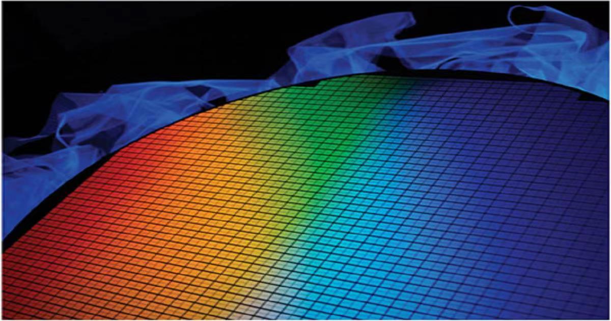
Silicon microelectronics is at the heart of modern electronics, finding applications in the computing, data processing, data storage, communications, and Internet of Things fields. Its development has been guided by Moore’s law since the 1970s and is now reaching its physical limits related to device dimension, integration density, and complexity both in CMOS and memory technologies. To overcome these limits, new challenges have been addressed regarding new material integration for FEOL and BEOL purposes, new processes for material growth, deposition, doping, etching and patterning, new device architectures for better scalability, improved physical characterization techniques for CD metrology, and advanced device and interconnect electrical characterization methodologies.

Dr. Gerard Ghibaudo
Dr. Francis Balestra
Topic Editors

Keywords

  • new materials
  • integration processes
  • device architectures
  • physical characterization and metrology
  • electrical characterization and reliability
  • CMOS
  • memories
  • cryogenic electronics
  • beyond CMOS
  • 3D integration

Participating Journals

Journal Name Impact Factor CiteScore Launched Year First Decision (median) APC
Applied Sciences
applsci
2.5 5.3 2011 18.4 Days CHF 2400 Submit
Electronics
electronics
2.6 5.3 2012 16.4 Days CHF 2400 Submit
Materials
materials
3.1 5.8 2008 13.9 Days CHF 2600 Submit
Applied Nano
applnano
- - 2020 25.4 Days CHF 1000 Submit
Technologies
technologies
4.2 6.7 2013 21.1 Days CHF 1600 Submit
Inventions
inventions
2.1 4.8 2016 18.5 Days CHF 1800 Submit
Chips
chips
- - 2022 22.2 Days CHF 1000 Submit

Preprints.org is a multidiscipline platform providing preprint service that is dedicated to sharing your research from the start and empowering your research journey.

MDPI Topics is cooperating with Preprints.org and has built a direct connection between MDPI journals and Preprints.org. Authors are encouraged to enjoy the benefits by posting a preprint at Preprints.org prior to publication:

  1. Immediately share your ideas ahead of publication and establish your research priority;
  2. Protect your idea from being stolen with this time-stamped preprint article;
  3. Enhance the exposure and impact of your research;
  4. Receive feedback from your peers in advance;
  5. Have it indexed in Web of Science (Preprint Citation Index), Google Scholar, Crossref, SHARE, PrePubMed, Scilit and Europe PMC.

Published Papers (39 papers)

Order results
Result details
Journals
Select all
Export citation of selected articles as:
21 pages, 6786 KiB  
Article
A Novel Multi-Mode Charge Pump in Word Line Driver for Compute-in-Memory Arrays
by Zhengyuan Lin, Xiaoyu Zhong, Zhiguo Yu, Yating Dong, Zengqi Huang and Xiaofeng Gu
Electronics 2025, 14(1), 175; https://doi.org/10.3390/electronics14010175 - 3 Jan 2025
Viewed by 466
Abstract
Flash memory, as the core unit of a compute-in-memory (CIM) array, requires multiple positive and negative (PN) high voltages (HVs) for word lines (WLs) to operate during storage and computation. A traditional WL driver generates these voltages using several charge pumps (CPs), leading [...] Read more.
Flash memory, as the core unit of a compute-in-memory (CIM) array, requires multiple positive and negative (PN) high voltages (HVs) for word lines (WLs) to operate during storage and computation. A traditional WL driver generates these voltages using several charge pumps (CPs), leading to significant area overhead. This paper presents a novel multi-mode CP (MMCP) that generates all required HVs for a CIM array under a single CP, supporting CIM unit operation in programming, readout, and erase modes. Unlike traditional voltage multipliers, the MMCP eliminates the need for multiple CPs, reducing area and pump capacitor usage. Compared to a PN CP that drives a common load, the MMCP can provide multiple PN HVs by using level shifters (LSs) and switches. The MMCP is designed in a 55 nm standard CMOS process with an area of only 0.021 mm2. Additionally, this paper proposes global PN HV switches, which can correctly deliver the PN HVs generated by the MMCP from the same port (at different times) to the upper and lower power rails of WL driver circuits. Simulation results show that with a 2.5 V supply, 100 pF load, and 50 μA current, the maximum error due to ripple is only 0.28%. Full article
Show Figures

Figure 1

36 pages, 6996 KiB  
Review
Organic–Inorganic Hybrid Dielectric Layers for Low-Temperature Thin-Film Transistors Applications: Recent Developments and Perspectives
by Javier Meza-Arroyo and Rafael Ramírez-Bon
Technologies 2025, 13(1), 20; https://doi.org/10.3390/technologies13010020 - 2 Jan 2025
Viewed by 806
Abstract
This paper reviews the recent development of organic–inorganic hybrid dielectric materials for application as gate dielectrics in thin-film transistors (TFTs). These hybrid materials consist of the blending of high-k inorganic dielectrics with polymers, and their resulting properties depend on the amount and type [...] Read more.
This paper reviews the recent development of organic–inorganic hybrid dielectric materials for application as gate dielectrics in thin-film transistors (TFTs). These hybrid materials consist of the blending of high-k inorganic dielectrics with polymers, and their resulting properties depend on the amount and type of interactions between the organic and inorganic phases. The resulting amorphous networks, characterized by crosslinked organic and inorganic phases, can be tailored for specific applications, including gate dielectrics in TFTs. As dielectric materials, they offer a synergistic combination of high dielectric constants, low leakage currents, and mechanical flexibility, crucial for next-generation flexible electronics. Furthermore, organic–inorganic hybrid materials are easily processed in solution, allowing for low-temperature deposition compatible with flexible substrates. Various configurations of these hybrid gate dielectrics, such as bilayer structures and polymer nanocomposites, are discussed, with an emphasis on their potential to enhance device performance. Despite the significant advancements, challenges remain in optimizing the performance and stability of these hybrid materials. This review summarizes recent progress and highlights the advantages and emerging applications of low-temperature, solution-processed hybrid dielectrics, with a focus on their integration into flexible, stretchable, and wearable electronic devices. Full article
Show Figures

Figure 1

12 pages, 11779 KiB  
Communication
Normally-Off Trench-Gated AlGaN/GaN Current Aperture Vertical Electron Transistor with Double Superjunction
by Jong-Uk Kim, Do-Yeon Park, Byeong-Jun Park and Sung-Ho Hahm
Technologies 2024, 12(12), 262; https://doi.org/10.3390/technologies12120262 - 16 Dec 2024
Viewed by 1030
Abstract
This study proposes an AlGaN/GaN current aperture vertical electron transistor (CAVET) featuring a double superjunction (SJ) to enhance breakdown voltage (BV) and investigates its electrical characteristics via technology computer-aided design (TCAD) Silvaco Atlas simulation. An additional p-pillar was formed beneath the gate [...] Read more.
This study proposes an AlGaN/GaN current aperture vertical electron transistor (CAVET) featuring a double superjunction (SJ) to enhance breakdown voltage (BV) and investigates its electrical characteristics via technology computer-aided design (TCAD) Silvaco Atlas simulation. An additional p-pillar was formed beneath the gate current blocking layer to create a lateral depletion region that provided a high off-state breakdown voltage. To address the tradeoff between the drain current and off-state breakdown voltage, the key design parameters were carefully optimized. The proposed device exhibited a higher off-state breakdown voltage (2933 V) than the device with a single SJ (2786 V), although the specific on-resistance of the proposed method (1.29 mΩ·cm−2) was slightly higher than that of the single SJ device (1.17 mΩ·cm−2). In addition, the reverse transfer capacitance was improved by 15.6% in the proposed device. Full article
Show Figures

Figure 1

11 pages, 2887 KiB  
Article
Spin Current Enhancement Using Double-Ferromagnetic-Layer Structure for Magnetoelectric Spin-Orbit Logic Device
by Bayartulga Ishdorj, Shumaila Sharif and Taehui Na
Electronics 2024, 13(20), 4085; https://doi.org/10.3390/electronics13204085 - 17 Oct 2024
Viewed by 732
Abstract
The use of Moore’s law appears to be coming to an end due to technological and physical constraints, as complementary metal-oxide semiconductor (CMOS) transistors become smaller and closer to the atomic scale. Therefore, various emerging technologies are being researched as potential successors to [...] Read more.
The use of Moore’s law appears to be coming to an end due to technological and physical constraints, as complementary metal-oxide semiconductor (CMOS) transistors become smaller and closer to the atomic scale. Therefore, various emerging technologies are being researched as potential successors to traditional CMOS transistors, and one of the most exciting candidates is the magnetoelectric spin-orbit (MESO) device. The MESO device comprises two portions (input and output) and it cascades charge/voltage as input and output signals. In the MESO device’s output portion, ferromagnetic (FM) and high-spin-orbit-coupling layers are employed to provide spin-polarized current and charge/voltage output. In this paper, we offer a description and analysis of the operating mechanism of the MESO device’s output portion using a spin flow approach and propose a double-FM-layer structure. In the double-FM-layer structure, we implement two FM layers with antiparallel magnetization directions, instead of using a single-FM-layer structure to increase the output charge/voltage. The proposed structure is verified through the Verilog-A compact model. Full article
Show Figures

Figure 1

16 pages, 533 KiB  
Article
Regularizing Lifetime Drift Prediction in Semiconductor Electrical Parameters with Quantile Random Forest Regression
by Lukas Sommeregger and Jürgen Pilz
Technologies 2024, 12(9), 165; https://doi.org/10.3390/technologies12090165 - 13 Sep 2024
Cited by 1 | Viewed by 2051
Abstract
Semiconductors play a crucial role in a wide range of applications and are integral to essential infrastructures. Manufacturers of these semiconductors must meet specific quality and lifetime targets. To estimate the lifetime of semiconductors, accelerated stress tests are conducted. This paper introduces a [...] Read more.
Semiconductors play a crucial role in a wide range of applications and are integral to essential infrastructures. Manufacturers of these semiconductors must meet specific quality and lifetime targets. To estimate the lifetime of semiconductors, accelerated stress tests are conducted. This paper introduces a novel approach to modeling drift in discrete electrical parameters within stress test devices. It incorporates a machine learning (ML) approach for arbitrary panel data sets of electrical parameters from accelerated stress tests. The proposed model involves an expert-in-the-loop MLOps decision process, allowing experts to choose between an interpretable model and a robust ML algorithm for regularization and fine-tuning. The model addresses the issue of outliers influencing statistical models by employing regularization techniques. This ensures that the model’s accuracy is not compromised by outliers. The model uses interpretable statistically calculated limits for lifetime drift and uncertainty as input data. It then predicts these limits for new lifetime stress test data of electrical parameters from the same technology. The effectiveness of the model is demonstrated using anonymized real data from Infineon technologies. The model’s output can help prioritize parameters by the level of significance for indication of degradation over time, providing valuable insights for the analysis and improvement of electrical devices. The combination of explainable statistical algorithms and ML approaches enables the regularization of quality control limit calculations and the detection of lifetime drift in stress test parameters. This information can be used to enhance production quality by identifying significant parameters that indicate degradation and detecting deviations in production processes. Full article
Show Figures

Figure 1

19 pages, 6118 KiB  
Article
A Small Database with an Adaptive Data Selection Method for Solder Joint Fatigue Life Prediction in Advanced Packaging
by Qinghua Su, Cadmus Yuan and Kuo-Ning Chiang
Materials 2024, 17(16), 4091; https://doi.org/10.3390/ma17164091 - 17 Aug 2024
Cited by 1 | Viewed by 1139
Abstract
There has always been high interest in predicting the solder joint fatigue life in advanced packaging with high accuracy and efficiency. Artificial Intelligence Plus (AI+) is becoming increasingly popular as computational facilities continue to develop. This study will introduce machine learning (a core [...] Read more.
There has always been high interest in predicting the solder joint fatigue life in advanced packaging with high accuracy and efficiency. Artificial Intelligence Plus (AI+) is becoming increasingly popular as computational facilities continue to develop. This study will introduce machine learning (a core component of AI). With machine learning, metamodels that approximate the attributes of systems or functions are created to predict the fatigue life of advanced packaging. However, the prediction ability is highly dependent on the size and distribution of the training data. Increasing the amount of training data is the most intuitive approach to improve prediction performance, but this implies a higher computational cost. In this research, the adaptive sampling methods are applied to build the machine learning model with a small dataset sampled from an existing database. The performance of the model will be visualized using predefined criteria. Moreover, ensemble learning can be used to improve the performance of AI models after they have been fully trained. Full article
Show Figures

Figure 1

12 pages, 3794 KiB  
Article
High Electron Mobility in Si-Doped Two-Dimensional β-Ga2O3 Tuned Using Biaxial Strain
by Hui Zeng, Chao Ma and Meng Wu
Materials 2024, 17(16), 4008; https://doi.org/10.3390/ma17164008 - 12 Aug 2024
Viewed by 1415
Abstract
Two-dimensional (2D) semiconductors have attracted much attention regarding their use in flexible electronic and optoelectronic devices, but the inherent poor electron mobility in conventional 2D materials severely restricts their applications. Using first-principles calculations in conjunction with Boltzmann transport theory, we systematically investigated the [...] Read more.
Two-dimensional (2D) semiconductors have attracted much attention regarding their use in flexible electronic and optoelectronic devices, but the inherent poor electron mobility in conventional 2D materials severely restricts their applications. Using first-principles calculations in conjunction with Boltzmann transport theory, we systematically investigated the Si-doped 2D β-Ga2O3 structure mediated by biaxial strain, where the structural stabilities were determined by formation energy, phonon spectrum, and ab initio molecular dynamic simulation. Initially, the band gap values of Si-doped 2D β-Ga2O3 increased slightly, followed by a rapid decrease from 2.46 eV to 1.38 eV accompanied by strain modulations from −8% compressive to +8% tensile, which can be ascribed to the bigger energy elevation of the σ* anti-bonding in the conduction band minimum than that of the π bonding in the valence band maximum. Additionally, band structure calculations resolved a direct-to-indirect transition under the tensile strains. Furthermore, a significantly high electron mobility up to 4911.18 cm2 V−1 s−1 was discovered in Si-doped 2D β-Ga2O3 as the biaxial tensile strain approached 8%, which originated mainly from the decreased quantum confinement effect on the surface. The electrical conductivity was elevated with the increase in tensile strain and the enhancement of temperature from 300 K to 800 K. Our studies demonstrate the tunable electron mobilities and band structures of Si-doped 2D β-Ga2O3 using biaxial strain and shed light on its great potential in nanoscale electronics. Full article
Show Figures

Figure 1

12 pages, 4144 KiB  
Article
Systematic Analysis of Spacer and Gate Length Scaling on Memory Characteristics in 3D NAND Flash Memory
by Hee Young Bae, Seul Ki Hong and Jong Kyung Park
Appl. Sci. 2024, 14(15), 6689; https://doi.org/10.3390/app14156689 - 31 Jul 2024
Cited by 1 | Viewed by 1415
Abstract
This study investigates the impact of oxide/nitride (ON) pitch scaling on the memory performance of 3D NAND flash memory. We aim to enhance 3D NAND flash memory by systematically reducing the spacer length (Ls) and gate length (Lg) to achieve improved memory characteristics. [...] Read more.
This study investigates the impact of oxide/nitride (ON) pitch scaling on the memory performance of 3D NAND flash memory. We aim to enhance 3D NAND flash memory by systematically reducing the spacer length (Ls) and gate length (Lg) to achieve improved memory characteristics. Using TCAD simulations, we evaluate the effects of Ls and Lg scaling on the program speed, erase speed, and Z-interference. Furthermore, we examine the influence of concave and convex channel structures in the context of Ls and Lg scaling. By analyzing the distributions of electron and hole-trapped charges, we provide insights into optimizing the trade-offs between the memory window and retention characteristics. This research offers valuable guidelines for improving the reliability and performance of 3D NAND flash memory through a systematic analysis of spacer and gate length scaling. Full article
Show Figures

Figure 1

25 pages, 10247 KiB  
Article
Development of Power-Delay Product Optimized ASIC-Based Computational Unit for Medical Image Compression
by Tanya Mendez, Tejasvi Parupudi, Vishnumurthy Kedlaya K and Subramanya G. Nayak
Technologies 2024, 12(8), 121; https://doi.org/10.3390/technologies12080121 - 29 Jul 2024
Cited by 2 | Viewed by 2333
Abstract
The proliferation of battery-operated end-user electronic devices due to technological advancements, especially in medical image processing applications, demands low power consumption, high-speed operation, and efficient coding. The design of these devices is centered on the Application-Specific Integrated Circuits (ASIC), General Purpose Processors (GPP), [...] Read more.
The proliferation of battery-operated end-user electronic devices due to technological advancements, especially in medical image processing applications, demands low power consumption, high-speed operation, and efficient coding. The design of these devices is centered on the Application-Specific Integrated Circuits (ASIC), General Purpose Processors (GPP), and Field Programmable Gate Array (FPGA) frameworks. The need for low-power functional blocks arises from the growing demand for high-performance computational units that are part of high-speed processors operating at high clock frequencies. The operational speed of the processor is determined by the computational unit, which is the workhorse of high-speed processors. A novel approach to integrating Very Large-Scale Integration (VLSI) ASIC design and the concepts of low-power VLSI compatible with medical image compression was embraced in this research. The focus of this study was the design, development, and implementation of a Power Delay Product (PDP) optimized computational unit targeted for medical image compression using ASIC design flow. This stimulates the research community’s quest to develop an ideal architecture, emphasizing on minimizing power consumption and enhancing device performance for medical image processing applications. The study uses area, delay, power, PDP, and Peak Signal-to-Noise Ratio (PSNR) as performance metrics. The research work takes inspiration from this and aims to enhance the efficiency of the computational unit through minor design modifications that significantly impact performance. This research proposes to explore the trade-off of high-performance adder and multiplier designs to design an ASIC-based computational unit using low-power techniques to enhance the efficiency in power and delay. The computational unit utilized for the digital image compression process was synthesized and implemented using gpdk 45 nm standard libraries with the Genus tool of Cadence. A reduced PDP of 46.87% was observed when the image compression was performed on a medical image, along with an improved PSNR of 5.89% for the reconstructed image. Full article
Show Figures

Figure 1

15 pages, 12241 KiB  
Article
Design and Characterization of a Digitally Tunable Gm-C Filter for Multi-Standard Receivers
by Mateus S. Oliveira, Matheus B. S. Carvalho, Crístian Müller, Lucas Compassi-Severo, Paulo C. C. de Aguirre and Alessandro G. Girardi
Electronics 2024, 13(14), 2866; https://doi.org/10.3390/electronics13142866 - 20 Jul 2024
Viewed by 1266
Abstract
This paper presents the design, simulation, prototyping, and measurement results of a digitally tunable fourth order Gm-C low-pass filter (LPF) for multi-standard radio receivers. The LPF cut-off frequency can be tunned by digitally selecting the transconductance of the basic reconfigurable operational transconductance amplifiers [...] Read more.
This paper presents the design, simulation, prototyping, and measurement results of a digitally tunable fourth order Gm-C low-pass filter (LPF) for multi-standard radio receivers. The LPF cut-off frequency can be tunned by digitally selecting the transconductance of the basic reconfigurable operational transconductance amplifiers (OTAs) that compose the circuit. Four operation modes allow for control of the OTA transconductances and, consequently, the scaling of power consumption. The filter was designed and prototyped in a 1.8 V 180 nm CMOS process. The measurement results indicate that the configurability provides a cutoff frequency of 1.90/3.56/6.07/8.15 MHz with a power consumption ranging from 9.9 to 13.1 mW. The designed filter achieves an IIP3 of 8.17 dBm for a signal bandwidth of 8.15 MHz. The performance, in terms of power dissipation, noise, and cut-off frequency, is at the same order of magnitude compared to recent related works reported in the literature. The advantages are a compact area, small sensitivity to component mismatches, and low design complexity. The proposed filter presents electrical characteristics suitable for the application in radio receivers for multi-carrier WCDMA signals. Full article
Show Figures

Figure 1

10 pages, 759 KiB  
Article
Technique of High-Field Electron Injection for Wafer-Level Testing of Gate Dielectrics of MIS Devices
by Dmitrii V. Andreev, Vladimir V. Andreev, Marina Konuhova and Anatoli I. Popov
Technologies 2024, 12(7), 102; https://doi.org/10.3390/technologies12070102 - 4 Jul 2024
Viewed by 1688
Abstract
We propose a technique for the wafer-level testing of the gate dielectrics of metal–insulator–semiconductor (MIS) devices by the high-field injection of electrons into the dielectric using a mode of increasing injection current density up to a set level. This method provides the capability [...] Read more.
We propose a technique for the wafer-level testing of the gate dielectrics of metal–insulator–semiconductor (MIS) devices by the high-field injection of electrons into the dielectric using a mode of increasing injection current density up to a set level. This method provides the capability to control a change in the charge state of the gate dielectric during all the testing. The proposed technique makes it possible to assess the integrity of the thin dielectric and at the same time to control the charge effects of its degradation. The method in particular can be used for manufacturing processes to control integrated circuits (ICs) based on MIS structures. In the paper, we propose an advanced algorithm of the Bounded J-Ramp testing of the gate dielectric and receive its approval when monitoring the quality of the gate dielectrics of production-manufactured MIS devices. We found that the maximum value of positive charge obtained when tested by the proposed method was a value close to that obtained when the charge was injected into the dielectric under a constant current with a Bounded J value despite large differences in the rate of degradation of the dielectric. Full article
Show Figures

Figure 1

20 pages, 2637 KiB  
Article
Survey of Security Issues in Memristor-Based Machine Learning Accelerators for RF Analysis
by Will Lillis, Max Cohen Hoffing and Wayne Burleson
Chips 2024, 3(2), 196-215; https://doi.org/10.3390/chips3020009 - 13 Jun 2024
Cited by 1 | Viewed by 1293
Abstract
We explore security aspects of a new computing paradigm that combines novel memristors and traditional Complimentary Metal Oxide Semiconductor (CMOS) to construct a highly efficient analog and/or digital fabric that is especially well-suited to Machine Learning (ML) inference processors for Radio Frequency (RF) [...] Read more.
We explore security aspects of a new computing paradigm that combines novel memristors and traditional Complimentary Metal Oxide Semiconductor (CMOS) to construct a highly efficient analog and/or digital fabric that is especially well-suited to Machine Learning (ML) inference processors for Radio Frequency (RF) signals. Analog and/or hybrid hardware designed for such application areas follows different constraints from that of traditional CMOS. This paradigm shift allows for enhanced capabilities but also introduces novel attack surfaces. Memristors have different properties than traditional CMOS which can potentially be exploited by attackers. In addition, the mixed signal approximate computing model has different vulnerabilities than traditional digital implementations. However both the memristor and the ML computation can be leveraged to create security mechanisms and countermeasures ranging from lightweight cryptography, identifiers (e.g., Physically Unclonable Functions (PUFs), fingerprints, and watermarks), entropy sources, hardware obfuscation and leakage/attack detection methods. Three different threat models are proposed: (1) Supply Chain, (2) Physical Attacks, and (3) Remote Attacks. For each threat model, potential vulnerabilities and defenses are identified. This survey reviews a variety of recent work from the hardware and ML security literature and proposes open problems for both attack and defense. The survey emphasizes the growing area of RF signal analysis and identification in terms of commercial space, as well as military applications and threat models. We differ from other recent surveys that target ML, in general, neglecting RF applications. Full article
Show Figures

Figure 1

10 pages, 4059 KiB  
Brief Report
A Simple Scan Driver Circuit Suitable for Depletion-Mode Metal-Oxide Thin-Film Transistors in Active-Matrix Displays
by Yikyoung You, Junhyung Lim, Kyoungseok Son, Jaybum Kim, Youngoo Kim, Kyunghoe Lee, Kyunghoon Chung and Keechan Park
Electronics 2024, 13(12), 2254; https://doi.org/10.3390/electronics13122254 - 8 Jun 2024
Cited by 1 | Viewed by 1229
Abstract
Metal-oxide (MOx) thin-film transistors (TFTs) require complex circuit structures to cope with their depletion mode characteristics, making them applicable only to large-area active matrix (AM) displays despite their low manufacturing cost and decent performance. In this paper, we report a simple MOx 10T-2C [...] Read more.
Metal-oxide (MOx) thin-film transistors (TFTs) require complex circuit structures to cope with their depletion mode characteristics, making them applicable only to large-area active matrix (AM) displays despite their low manufacturing cost and decent performance. In this paper, we report a simple MOx 10T-2C scan driver circuit that overcomes the depletion mode characteristics using a series-connected two transistor (STT) configuration and clock signals with two kinds of low-voltage levels. The proposed circuit has a wide operating range of TFT characteristics, i.e., −2.8 V ≤ VTH ≤ +3.0 V. Through the measurement results of the manufactured sample, it was confirmed that the performance and area of our circuit are suitable for high-resolution mobile displays. Full article
Show Figures

Figure 1

14 pages, 2892 KiB  
Article
Directed Acyclic Graph-Based Datapath Synthesis Using Graph Isomorphism and Gate Reconfiguration
by Liuting Shang, Sheng Lu, Yichen Zhang, Sungyong Jung and Chenyun Pan
Chips 2024, 3(2), 182-195; https://doi.org/10.3390/chips3020008 - 4 Jun 2024
Viewed by 1355
Abstract
Datapath synthesis is a crucial step in synthesis flow and aims at globally minimizing an area by identifying shareable logic structures. This paper introduces a novel Directed Acyclic Graph (DAG)-based datapath synthesis method based on graph isomorphism and gate reconfiguration. Unlike algorithms that [...] Read more.
Datapath synthesis is a crucial step in synthesis flow and aims at globally minimizing an area by identifying shareable logic structures. This paper introduces a novel Directed Acyclic Graph (DAG)-based datapath synthesis method based on graph isomorphism and gate reconfiguration. Unlike algorithms that identify common specification logic, our approach simplifies the problem by focusing on searching for common topology. Leveraging the concept of gate reconfiguration, our algorithm extends the applicability of DAG-based datapath synthesis by transforming a topology-equivalent network into a specification-equivalent network. Experimental results demonstrate up to 23.6% improvement when optimizing the adder–subtractor circuit, a scenario not addressed by existing DAG-based datapath synthesis algorithms. Full article
Show Figures

Figure 1

29 pages, 7625 KiB  
Review
A Review on Fundamentals of Noise-Shaping SAR ADCs and Design Considerations
by Victor H. Arzate-Palma, David G. Rivera-Orozco, Gerardo Molina Salgado and Federico Sandoval-Ibarra
Chips 2024, 3(2), 153-181; https://doi.org/10.3390/chips3020007 - 10 May 2024
Viewed by 3111
Abstract
A general overview of Noise-Shaping Successive Approximation Register (SAR) analog-to-digital converters is provided, encompassing the fundamentals, operational principles, and key architectures of Noise-Shaping SAR (NS SAR). Key challenges, including inherent errors in processing circuits, are examined, along with current advancements in architecture design. [...] Read more.
A general overview of Noise-Shaping Successive Approximation Register (SAR) analog-to-digital converters is provided, encompassing the fundamentals, operational principles, and key architectures of Noise-Shaping SAR (NS SAR). Key challenges, including inherent errors in processing circuits, are examined, along with current advancements in architecture design. Various issues, such as loop filter optimization, implementation methods, and DAC network element mismatches, are explored, along with considerations for voltage converter performance. The design of dynamic comparators is examined, highlighting their critical role in the SAR ADC architecture. Various architectures of dynamic comparators are extensively explored, including optimization techniques, performance considerations, and emerging trends. Finally, emerging trends and future challenges in the field are discussed. Full article
Show Figures

Figure 1

12 pages, 2921 KiB  
Article
Study of Acoustic Emission from the Gate of Gallium Nitride High Electron Mobility Transistors
by Bartłomiej K. Paszkiewicz, Bogdan Paszkiewicz and Andrzej Dziedzic
Electronics 2024, 13(10), 1840; https://doi.org/10.3390/electronics13101840 - 9 May 2024
Viewed by 1157
Abstract
Nitrides are the leading semiconductor material used for the fabrication of high electron mobility transistors (HEMTs). They exhibit piezoelectric properties, which, coupled with their high mechanical stiffness, expand their versatile applications into the fabrication of piezoelectric devices. Today, due to advances in device [...] Read more.
Nitrides are the leading semiconductor material used for the fabrication of high electron mobility transistors (HEMTs). They exhibit piezoelectric properties, which, coupled with their high mechanical stiffness, expand their versatile applications into the fabrication of piezoelectric devices. Today, due to advances in device technology that result in a reduction in the size of individual transistor elements and due to increased structural complexity (e.g., multi-gate transistors), the integration of piezoelectric materials into HEMTs leads to an interesting occurrence, namely acoustic emission from the transistor gate due to piezoelectric effects. This could affect the device’s performance, reliability, and durability. However, this phenomenon has not yet been comprehensively described. This paper aims to examine this overlooked aspect of AlGaN/GaN HEMT operation, that is, the acoustic emission from the gate region of the device induced by piezoelectric effects. For this purpose, dedicated test structures were designed, consisting of two narrow 1.7 μm-wide metallization strips placed at distances ranging from 5 μm to 200 μm fabricated in AlGaN/GaN heterostructures to simulate and examine the gate behavior of the HEMT transistor. For comparison, the test device structures were also fabricated on sapphire, which is not a piezoelectric material. Measurements of acoustic and electrical interactions in the microwave range were carried out using the “on wafer” method with Picoprobe’s signal–ground–signal (SGS)-type microwave probes. The dependence of reflectance |S11| and transmittance |S21| vs. frequency was investigated, and the coupling capacitance was determined. An equivalent circuit model of the test structure was developed, and finite element method simulation was performed to study the distribution of the acoustic wave in the nitride layers and substrate for different frequencies using Comsol Multiphysics software. At frequencies up to 2–3 GHz, the formation of volume waves and a surface wave, capable of propagating over long distances (in the order of tens of micrometers) was observed. At higher frequencies, the resulting distribution of displacements as a result of numerous reflections and interferences was more complicated. However, there was always the possibility of a surface wave occurrence, even at large distances from the excitation source. At small gate distances, electrical interactions dominate. Above 100 µm, electrical interactions are comparable to acoustic ones. With further increases in distance, weakly attenuated surface waves will dominate. Full article
Show Figures

Figure 1

24 pages, 18551 KiB  
Article
A CMOS 12-Bit 3MS/s Rad-Hard Digital-to-Analog Converter Based on a High-Linearity Resistor String Poly-Matrix
by Cristiano Calligaro and Umberto Gatti
Chips 2024, 3(2), 129-152; https://doi.org/10.3390/chips3020006 - 8 May 2024
Cited by 1 | Viewed by 2011
Abstract
This work presents a rad-hard 12-bit 3 MS/s resistor string DAC for space applications. The converter has been developed using rad-hardened techniques both at architecture and layout levels starting from a conventional topology. The design considers the different effects of the radiation that [...] Read more.
This work presents a rad-hard 12-bit 3 MS/s resistor string DAC for space applications. The converter has been developed using rad-hardened techniques both at architecture and layout levels starting from a conventional topology. The design considers the different effects of the radiation that could damage the circuits in space environments. The DAC has been developed and integrated a standard CMOS 0.13 μm technology by IHP, using RHBD techniques. Low Earth Orbit (LEO) requires a TID value of around 100 krad (Si), according to the expected length of the mission. The temperature range is between −55 °C and 125 °C. The DAC power budget is similar to that of terrestrial applications. The measured INL (Integral Non-Linearity) and DNL (Differential Non-Linearity) are better than 0.2 LSB, while the ENOB (Effective Number Of Bits) at a 3 MS/s clock exceeds 9.7 bits while loading a 10 pF capacitor. The DAC has been characterized under radiation, showing a fluctuation in the analog output lower than 2 LSB (mainly due to measurement uncertainty) up to 500 krad (Si). Power consumption shows a negligible increase, too. A 10-bit version of the same DAC as the downscaled 12-bit one has been developed as well. Full article
Show Figures

Figure 1

21 pages, 989 KiB  
Article
SpikeExplorer: Hardware-Oriented Design Space Exploration for Spiking Neural Networks on FPGA
by Dario Padovano, Alessio Carpegna, Alessandro Savino and Stefano Di Carlo
Electronics 2024, 13(9), 1744; https://doi.org/10.3390/electronics13091744 - 1 May 2024
Cited by 2 | Viewed by 1890
Abstract
One of today’s main concerns is to bring artificial intelligence capabilities to embedded systems for edge applications. The hardware resources and power consumption required by state-of-the-art models are incompatible with the constrained environments observed in edge systems, such as IoT nodes and wearable [...] Read more.
One of today’s main concerns is to bring artificial intelligence capabilities to embedded systems for edge applications. The hardware resources and power consumption required by state-of-the-art models are incompatible with the constrained environments observed in edge systems, such as IoT nodes and wearable devices. Spiking Neural Networks (SNNs) can represent a solution in this sense: inspired by neuroscience, they reach unparalleled power and resource efficiency when run on dedicated hardware accelerators. However, when designing such accelerators, the amount of choices that can be taken is huge. This paper presents SpikExplorer, a modular and flexible Python tool for hardware-oriented Automatic Design Space Exploration to automate the configuration of FPGA accelerators for SNNs. SpikExplorer enables hardware-centric multiobjective optimization, supporting target factors such as accuracy, area, latency, power, and various combinations during the exploration process. The tool searches the optimal network architecture, neuron model, and internal and training parameters leveraging Bayesian optimization, trying to reach the desired constraints imposed by the user. It allows for a straightforward network configuration, providing the full set of explored points for the user to pick the trade-off that best fits their needs. The potential of SpikExplorer is showcased using three benchmark datasets. It reaches 95.8% accuracy on the MNIST dataset, with a power consumption of 180 mW/image and a latency of 0.12 ms/image, making it a powerful tool for automatically optimizing SNNs. Full article
Show Figures

Figure 1

18 pages, 5491 KiB  
Article
FATE: A Flexible FPGA-Based Automatic Test Equipment for Digital ICs
by Jin Zhang, Zhenghui Liu, Xiao Hu, Peixin Liu, Zhiling Hu and Lidan Kuang
Electronics 2024, 13(9), 1667; https://doi.org/10.3390/electronics13091667 - 26 Apr 2024
Viewed by 1875
Abstract
The limits of chip technology are constantly being pushed with the continuous development of integrated circuit manufacturing processes and equipment. Currently, chips contain several billion, and even tens of billions, of transistors, making chip testing increasingly challenging. The verification of very large-scale integrated [...] Read more.
The limits of chip technology are constantly being pushed with the continuous development of integrated circuit manufacturing processes and equipment. Currently, chips contain several billion, and even tens of billions, of transistors, making chip testing increasingly challenging. The verification of very large-scale integrated circuits (VLSI) requires testing on specialized automatic test equipment (ATE), but their cost and size significantly limit their applicability. The current FPGA-based ATE is limited in its scalability and support for few test channels and short test vector lengths. As a result, it is only suitable for testing specific chips in small-scale circuits and cannot be used to test VLSI. This paper proposes a low-cost hardware and software solution for testing digital integrated circuits based on design for testability (DFT) on chips, which enables the functional and performance test of the chip. The solution proposed can effectively use the resources within the FPGA to provide additional test channels. Furthermore, the round-robin data transmission mode can also support test vectors of any length and it can satisfy different types of chip test projects through the dynamic configuration of each test channel. The experiment successfully tested a digital signal processor (DSP) chip with 72 scan test pins (theoretically supporting 160 test pins). Compared to our previous work, the work in this paper increases the number of test channels by four times while reducing resource utilization per channel by 37.5%, demonstrating good scalability and versatility. Full article
Show Figures

Figure 1

15 pages, 547 KiB  
Article
A Power-Efficient High-Drive Current Mirror Combining a Regulated Cascode Topology with a Non-Linear CCII-Based Feedback
by Mohan Julien, Serge Bernard, Fabien Soulier, Vincent Kerzérho and Guy Cathébras
Electronics 2024, 13(8), 1556; https://doi.org/10.3390/electronics13081556 - 19 Apr 2024
Viewed by 1138
Abstract
This brief presents a continuously regulated current mirror topology capable of providing a wide range of currents with high-precision and speed control features. The circuit combines a non-linear current-mode feedback solution for fast and energy-efficient operation with an input-referred regulated-cascode configuration for precise [...] Read more.
This brief presents a continuously regulated current mirror topology capable of providing a wide range of currents with high-precision and speed control features. The circuit combines a non-linear current-mode feedback solution for fast and energy-efficient operation with an input-referred regulated-cascode configuration for precise current mirroring. The proposed implementation has an output current ranging from 100 μA to 2 mA, exhibits a fast response time of ≈100 ns for the full range steps, while ensuring a high power efficiency (>90%) and low current copy errors (<0.5%). Full article
Show Figures

Figure 1

12 pages, 3186 KiB  
Article
Characteristics Analysis of IGZO TFT and Logic Unit in the Temperature Range of 8–475 K
by Jianjian Wang, Jinshun Bi, Gaobo Xu and Mengxin Liu
Electronics 2024, 13(8), 1427; https://doi.org/10.3390/electronics13081427 - 10 Apr 2024
Cited by 2 | Viewed by 1895
Abstract
The effect of high- and low-temperature conditions on the performance of IGZO TFT and logic circuits were investigated in this work. In the temperature range of 250−350 K, the performance of the IGZO TFT did not show significant changes and exhibited a certain [...] Read more.
The effect of high- and low-temperature conditions on the performance of IGZO TFT and logic circuits were investigated in this work. In the temperature range of 250−350 K, the performance of the IGZO TFT did not show significant changes and exhibited a certain degree of high- and low-temperature resistance. When the temperature was below 250 K, as the temperature decreased, the threshold voltage (VTH) of the IGZO TFT significantly increased, the field effect mobility (μFE) and the on state current (ION) significantly decreased. This is attributed to the lower excitation degree of charge carriers at extremely low temperatures, resulting in fewer charge carriers transitioning to the conduction or valence bands, and the formation of defects also limits carrier migration. When the temperature exceeded 350 K, as the temperature increased, more electrons could escape from the bandgap trap state and become free charge carriers, and the IGZO layer was thermally excited to produce more oxygen vacancies, resulting in higher μFE and lower VTH. In addition, the drain current noise spectral density of IGZO TFT conformed to the 1/ƒ noise characteristic, and the degradation mechanism of IGZO TFT over a wide temperature range was confirmed based on the changes in noise spectral density at different temperatures. In addition, an inverter logic unit circuit was designed based on IGZO TFT, and the performance changes over a wide temperature range were analyzed. This lays the foundation for IGZO TFT to be applied in integrated circuits with harsh environments. Full article
Show Figures

Figure 1

21 pages, 14349 KiB  
Article
A 0.49–4.34 μW LC-SAR Hybrid ADC with a 10.85-Bit ENOB and 20 KS/s Bandwidth
by Hai Tang, Weilin Xu, Haiou Li, Baolin Wei and Xueming Wei
Electronics 2024, 13(6), 1078; https://doi.org/10.3390/electronics13061078 - 14 Mar 2024
Viewed by 1135
Abstract
This paper presents a level-crossing successive-approximation-register (LC-SAR) hybrid analog-to-digital converter (ADC) that combines an LC ADC with an SAR ADC, which may be used for Internet of Things (IoT) random sparse event scenarios. The sampling frequency of a traditional LC ADC is usually [...] Read more.
This paper presents a level-crossing successive-approximation-register (LC-SAR) hybrid analog-to-digital converter (ADC) that combines an LC ADC with an SAR ADC, which may be used for Internet of Things (IoT) random sparse event scenarios. The sampling frequency of a traditional LC ADC is usually proportional to the maximum instantaneous rate of change of the input signal; therefore, a higher input signal frequency inevitably leads to higher system power consumption. However, the proposed hybrid ADC uses the input level difference between the two moments before and after level-crossing detection, thereby ensuring a higher conversion precision and lower power consumption, even at higher input signal frequencies. Compared with traditional LC ADC or SAR ADC, the proposed hybrid ADC combines the ultralow-power advantage of LC ADC with the high-precision advantage of SAR ADC in converting IoT data with sparse characteristics such as ECG, EEG, and brain potential. The LC-SAR hybrid ADC is designed with a 0.18 μm CMOS process and consumes 4.34 μW at a 1.8 V supply voltage, achieving an SNDR of 67.41 dB and a bandwidth of 20 kHz. The spectrum analysis result was 10.85 ENOB when the input sinusoidal signal was 14.975 kHz. When inputted with an ECG signal, the system power consumption was as low as 0.49 μW. Furthermore, the proposed hybrid ADC obtained a good figure of merit, with FoMw and FoMs reaching 58.8 fJ/conv.steps and 164 dB, respectively. Compared to a conventional uniform sampling ADC, approximately 80% of the power savings and an 8x compression ratio can be achieved in physiological signal acquisition applications. Full article
Show Figures

Figure 1

28 pages, 5087 KiB  
Article
Optimal Implementations of 8b/10b Encoders and Decoders for AMD FPGAs
by Stefan Popa, Mihai Ivanovici and Radu-Mihai Coliban
Electronics 2024, 13(6), 1062; https://doi.org/10.3390/electronics13061062 - 13 Mar 2024
Cited by 1 | Viewed by 1908
Abstract
The 8b/10b IBM encoding scheme is used in a plethora of communication technologies, including USB, Gigabit Ethernet, and Serial ATA. We propose two primitive-based structural designs of an 8b/10b encoder and two of an 8b/10b decoder, all targeted at modern AMD FPGA architectures. [...] Read more.
The 8b/10b IBM encoding scheme is used in a plethora of communication technologies, including USB, Gigabit Ethernet, and Serial ATA. We propose two primitive-based structural designs of an 8b/10b encoder and two of an 8b/10b decoder, all targeted at modern AMD FPGA architectures. Our aim is to reduce the amount of resources used for the implementations. We compare our designs with implementations resulting from behavioral models as well as with state-of-the-art solutions from the literature. The implementation results show that our solutions provide the lowest resource utilization with comparable maximum operating frequency and power consumption. The proposed structural designs are suitable for resource-constrained data communication protocol implementations that employ the IBM 8b/10b encoding scheme. This paper is an extended version of our paper published at the 2022 International Symposium on Electronics and Telecommunications (ISETC), Timisoara, Romania, 10–11 November 2022. Full article
Show Figures

Figure 1

11 pages, 7784 KiB  
Article
Low-Temperature Diffusion of Au and Ag Nanolayers for Cu Bonding
by Sangmin Lee, Sangwoo Park and Sarah Eunkyung Kim
Appl. Sci. 2024, 14(1), 147; https://doi.org/10.3390/app14010147 - 23 Dec 2023
Cited by 1 | Viewed by 2097
Abstract
With the recent rapid development of IT technology, the demand for multifunctional semiconductor devices capable of high performance has increased rapidly, and the miniaturization of such devices has also faced limitations. To overcome these limitations, various studies have investigated three-dimensional packaging methods of [...] Read more.
With the recent rapid development of IT technology, the demand for multifunctional semiconductor devices capable of high performance has increased rapidly, and the miniaturization of such devices has also faced limitations. To overcome these limitations, various studies have investigated three-dimensional packaging methods of stacking devices, and among them, hybrid bonding is being actively conducted during the bonding process. studies of hybrid bonding during the bonding process are active. In this study, Cu bonding using a nano passivation layer was carried out for Cu/SiO2 hybrid bonding applications, with Au and Ag deposited on Cu at the nano level and used as a protective layer to prevent Cu oxidation and to achieve low-temperature Cu bonding. Au was deposited at about 12 nm, and Ag was deposited at about 15 nm, with Cu bonding carried out at 180 °C for 30 min, after which an annealing process was conducted at 200 °C for one hour. After bonding, the specimen was diced into a 1 cm × 1 cm chip, and the bonding interface was analyzed using SEM and TEM. Additionally, the 1 cm × 1 cm chip was diced into 2 mm × 2 mm specimens to measure the shear strength of the bonded chip, and the average shear strength of Au and Ag was found to be 5.4 and 6.6 MPa, respectively. The degree of diffusion between Au-Cu and Ag-Cu was then investigated; the diffusion activation energy when Au diffuses to Cu was 6369.52 J/mol, and the diffusion activation energy when Ag diffuses to Cu was 17,933.21 J/mol. Full article
Show Figures

Figure 1

14 pages, 1891 KiB  
Communication
A 55 nm CMOS RF Transmitter Front-End with an Active Mixer and a Class-E Power Amplifier for 433 MHz ISM Band Applications
by Huazhong Yuan, Ranran Zhou, Peng Wang, Hui Xu and Yong Wang
Electronics 2023, 12(22), 4711; https://doi.org/10.3390/electronics12224711 - 20 Nov 2023
Viewed by 1403
Abstract
In order to meet the increasing demands of wireless communication for ISM bands, a 433 MHz transmitter RF front-end is designed using a 55 nm low-power CMOS technology. The circuits consist of an active mixer, a driver amplifier and a class-E power amplifier [...] Read more.
In order to meet the increasing demands of wireless communication for ISM bands, a 433 MHz transmitter RF front-end is designed using a 55 nm low-power CMOS technology. The circuits consist of an active mixer, a driver amplifier and a class-E power amplifier (PA). A double-balanced Gilbert active mixer is designed to realize binary phase-shift keying (BPSK) modulation. The driver is used to preamplify the modulated RF signals. The class-E PA adopts a parallel four-branch cascode structure to control the output power level. The load network of the PA is implemented through an off-chip circuit, in which a finite DC-feed inductance load network is selected to reduce the power loss. The mixer and driver are designed with a 1.2 V supply voltage, while the PA is operated at a 1.8 V supply voltage. The area of the chip is 0.206 mm × 0.089 mm, and the measured results show that it achieves a maximum output power of 2.7 dBm, with a total power consumption of 6.72 mW. At a drain efficiency (DE) of 34.5%, an S22 less than −10 dB over the frequency ranges from 393.79 MHz to 455.70 MHz can be measured for the PA. With 192 kbps BPSK data modulated at 433 MHz, the measured EVM is about 0.83% rms. Full article
Show Figures

Figure 1

16 pages, 7478 KiB  
Article
Role of Native Defects in Fe-Doped β-Ga2O3
by Hui Zeng, Meng Wu, Haixia Gao, Yuansheng Wang, Hongfei Xu, Meijuan Cheng and Qiubao Lin
Materials 2023, 16(20), 6758; https://doi.org/10.3390/ma16206758 - 19 Oct 2023
Cited by 5 | Viewed by 1992
Abstract
Iron impurities are believed to act as deep acceptors that can compensate for the n-type conductivity in as-grown Ga2O3, but several scientific issues, such as the site occupation of the Fe heteroatom and the complexes of Fe-doped β-Ga2 [...] Read more.
Iron impurities are believed to act as deep acceptors that can compensate for the n-type conductivity in as-grown Ga2O3, but several scientific issues, such as the site occupation of the Fe heteroatom and the complexes of Fe-doped β-Ga2O3 with native defects, are still lacking. In this paper, based on first-principle density functional theory calculations with the generalized gradient approximation approach, the controversy regarding the preferential Fe incorporation on the Ga site in the β-Ga2O3 crystal has been addressed, and our result demonstrates that Fe dopant is energetically favored on the octahedrally coordinated Ga site. The structural stabilities are confirmed by the formation energy calculations, the phonon dispersion relationships, and the strain-dependent analyses. The thermodynamic transition level Fe3+/Fe2+ is located at 0.52 eV below the conduction band minimum, which is consistent with Ingebrigtsen’s theoretical conclusion, but slightly smaller than some experimental values between 0.78 eV and 1.2 eV. In order to provide direct guidance for material synthesis and property design in Fe-doped β-Ga2O3, the defect formation energies, charge transitional levels, and optical properties of the defective complexes with different kinds of native defects are investigated. Our results show that VGa and Oi can be easily formed for the Fe-doped β-Ga2O3 crystals under O-rich conditions, where the +3 charge state FeGaGai and −2 charge state FeGaOi are energetically favorable when the Fermi level approaches the valence and conduction band edges, respectively. Optical absorption shows that the complexes of FeGaGai and FeGaVGa can significantly enhance the optical absorption in the visible-infrared region, while the energy-loss function in the β-Ga2O3 material is almost negligible after the extra introduction of various intrinsic defects. Full article
Show Figures

Figure 1

18 pages, 7221 KiB  
Article
Investigation of Trap Density Effect in Gate-All-Around Field Effect Transistors Using the Finite Element Method
by Maissa Belkhiria, Fatma Aouaini, Shatha A. Aldaghfag, Fraj Echouchene and Hafedh Belmabrouk
Electronics 2023, 12(17), 3673; https://doi.org/10.3390/electronics12173673 - 31 Aug 2023
Cited by 2 | Viewed by 1973
Abstract
Trap density refers to the density of electronic trap states within dielectric materials that can capture and release charge carriers (electrons or holes) in a semiconductor channel, affecting the transistor’s performance. This study aims to investigate the influence of trap density on the [...] Read more.
Trap density refers to the density of electronic trap states within dielectric materials that can capture and release charge carriers (electrons or holes) in a semiconductor channel, affecting the transistor’s performance. This study aims to investigate the influence of trap density on the electrothermal behavior of nanowire gate-all-around GAAFET devices. The numerical solution of Poisson’s equations and continuity equations, coupled with the heat conduction model, has been used to predict the temperature inside the GAAFET device. The finite element method has been used to discretize the semiconductor equations. Investigations have been carried out on a number of physical and geometric parameters, such as oxide thickness, nanowire radius, and gate length. Their effects on output characteristics and device temperature have been discussed. A thinner oxide thickness, lower device radius, and longer channel length led to a higher current flow. Results also reveal that high trap densities can have significant impacts on the degradation of electronic devices, particularly in the context of semiconductor devices like transistors. Full article
Show Figures

Figure 1

10 pages, 2028 KiB  
Article
Effects of Cu, Zn Doping on the Structural, Electronic, and Optical Properties of α-Ga2O3: First-Principles Calculations
by Hui Zeng, Meng Wu, Meijuan Cheng and Qiubao Lin
Materials 2023, 16(15), 5317; https://doi.org/10.3390/ma16155317 - 28 Jul 2023
Cited by 3 | Viewed by 1968
Abstract
The intrinsic n-type conduction in Gallium oxides (Ga2O3) seriously hinders its potential optoelectronic applications. Pursuing p-type conductivity is of longstanding research interest for Ga2O3, where the Cu- and Zn-dopants serve as promising candidates in monoclinic [...] Read more.
The intrinsic n-type conduction in Gallium oxides (Ga2O3) seriously hinders its potential optoelectronic applications. Pursuing p-type conductivity is of longstanding research interest for Ga2O3, where the Cu- and Zn-dopants serve as promising candidates in monoclinic β-Ga2O3. However, the theoretical band structure calculations of Cu- and Zn-doped in the allotrope α-Ga2O3 phase are rare, which is of focus in the present study based on first-principles density functional theory calculations with the Perdew–Burke–Ernzerhof functional under the generalized gradient approximation. Our results unfold the predominant Cu1+ and Zn2+ oxidation states as well as the type and locations of impurity bands that promote the p-type conductivity therein. Furthermore, the optical calculations of absorption coefficients demonstrate that foreign Cu and Zn dopants induce the migration of ultraviolet light to the visible–infrared region, which can be associated with the induced impurity 3d orbitals of Cu- and Zn-doped α-Ga2O3 near the Fermi level observed from electronic structure. Our work may provide theoretical guidance for designing p-type conductivity and innovative α-Ga2O3-based optoelectronic devices. Full article
Show Figures

Figure 1

49 pages, 13251 KiB  
Article
Survey of Reliability Research on 3D Packaged Memory
by Shuai Zhou, Kaixue Ma, Yugong Wu, Peng Liu, Xianghong Hu, Guojian Nie, Yan Ren, Baojun Qiu, Nian Cai, Shaoqiu Xu and Han Wang
Electronics 2023, 12(12), 2709; https://doi.org/10.3390/electronics12122709 - 17 Jun 2023
Cited by 3 | Viewed by 3994
Abstract
As the core carrier of information storage, a semiconductor memory device is a basic product with a large volume that is widespread in the integrated circuit industry. With the rapid development of semiconductor manufacturing processes and materials, the internal structure of memory has [...] Read more.
As the core carrier of information storage, a semiconductor memory device is a basic product with a large volume that is widespread in the integrated circuit industry. With the rapid development of semiconductor manufacturing processes and materials, the internal structure of memory has gradually shifted from a 2D planar packaging structure to a 3D packaging structure to meet industry demands for high-frequency, high-speed, and large-capacity devices with low power consumption. However, advanced 3D packaging technology can pose some reliability risks, making devices prone to failure, especially when used in harsh environmental conditions, including temperature changes, high temperature and humidity levels, and mechanical stress. In this paper, the authors introduce the typical structure characteristics of 3D packaged memory; analyze the reasons for device failure caused by stress; summarize current research methods that utilize temperature, mechanical and hygrothermal theories, and failure models; and present future challenges and directions regarding the reliability research of 3D packaged memory. Full article
Show Figures

Figure 1

12 pages, 3227 KiB  
Article
A Novel Word Line Driver Circuit for Compute-in-Memory Based on the Floating Gate Devices
by Xiaofeng Gu, Rao Che, Yating Dong and Zhiguo Yu
Electronics 2023, 12(5), 1185; https://doi.org/10.3390/electronics12051185 - 1 Mar 2023
Cited by 1 | Viewed by 2504
Abstract
In floating gate compute-in-memory (CIM) chips, due to the gate equivalent capacitance of the large-scale array and the parasitic capacitance of the long-distance transmission wire, it is difficult to balance the switching speed and area of the word line driver circuit (WLDC). The [...] Read more.
In floating gate compute-in-memory (CIM) chips, due to the gate equivalent capacitance of the large-scale array and the parasitic capacitance of the long-distance transmission wire, it is difficult to balance the switching speed and area of the word line driver circuit (WLDC). The difference among multiple voltage domains required for floating gate CIM devices has also far exceeded the withstand voltage range of a single transistor in the WLDC. This paper proposes a novel WLDC based on the working principle of the CIM array. A multi-level pre-processing voltage control method is adopted to carry out an optional hierarchical transmission of multiple high voltages, significantly reducing the propagation delay. The proposed WLDC is based on the Wilson current mirror structure, which substantially reduces the physical design area. The simulation results show that the circuit can convert a 1.2 V low-voltage domain input signal with a frequency of 10 MHz into a high-voltage domain output voltage, and the output voltage range of a single WLDC can reach −10 V to 10 V. With a capacitive load within 5 pF, the transmission delay is less than 10 ns. The layout area is 594.88 µm2, which is suitable for a large-scale CIM array. Full article
Show Figures

Figure 1

15 pages, 3484 KiB  
Article
Modeling on Monolithic Integration Structure of AlGaN/InGaN/GaN High Electron Mobility Transistors and LEDs: 2DEG Density and Radiative Recombination
by Yuan An, Kailin Ren, Luqiao Yin and Jianhua Zhang
Electronics 2023, 12(5), 1087; https://doi.org/10.3390/electronics12051087 - 22 Feb 2023
Cited by 2 | Viewed by 2847
Abstract
The monolithic integration structure of the AlGaN/InGaN/GaN−based high electron mobility transistor (HEMT) and light−emitting diode (LED) is attractive in LED lighting and visible light communication (VLC) systems owing to the reduction in parasitic elements by removing metal interconnections. Due to the band−offset and [...] Read more.
The monolithic integration structure of the AlGaN/InGaN/GaN−based high electron mobility transistor (HEMT) and light−emitting diode (LED) is attractive in LED lighting and visible light communication (VLC) systems owing to the reduction in parasitic elements by removing metal interconnections. Due to the band−offset and polarization effect, inserting a certain thickness in the InGaN layer into the traditional AlGaN/GaN single heterostructure increases the density of 2DEG to nearly twice the original. At the same time, inserting the InGaN quantum well layer can also improve the luminous efficiency of LED. In this paper, the physical models of two−dimensional electron gas (2DEG) densities and the threshold voltage of AlGaN/InGaN/GaN HEMTs are established and verified with experimental results from the literature. According to the calculation results, the two−dimensional electron gas (2DEG) density in the AlGaN/InGaN/GaN HEMT is 1.47 × 1013 cm−2, and the two−dimensional hole gas (2DHG) density is 0.55 × 1013 cm−2, when Al% = 0.2, In% = 0.1, dAlGaN = 20 nm. In addition, a physical model for the radiative recombination rate in the monolithic integration structure of HEMT−LED is proposed. This work provides a design guideline for AlGaN/InGaN/GaN HEMT and its application in visible light communication systems. Full article
Show Figures

Figure 1

16 pages, 847 KiB  
Article
A Fully Differential Difference Transconductance Amplifier Topology Based on CMOS Inverters
by Otávio Soares Silva, Rodrigo Aparecido da Silva Braga, Paulo Marcos Pinto, Luís Henrique de Carvalho Ferreira and Gustavo Della Colletta
Electronics 2023, 12(4), 963; https://doi.org/10.3390/electronics12040963 - 15 Feb 2023
Cited by 1 | Viewed by 3246
Abstract
This manuscript presents a fully differential difference transconductance amplifier (FDDTA) architecture based on CMOS inverters. Designed in a 130-nm CMOS process it operates in weak inversion when supplied with 0.25 V. In addition, the FDDTA requires no supplementary external calibration circuit, like tail [...] Read more.
This manuscript presents a fully differential difference transconductance amplifier (FDDTA) architecture based on CMOS inverters. Designed in a 130-nm CMOS process it operates in weak inversion when supplied with 0.25 V. In addition, the FDDTA requires no supplementary external calibration circuit, like tail current or bias voltage sources, since it relies on the distributed layout technique that intrinsically matches the CMOS inverters. For analytical purposes, we carried out a detailed investigation that describes all the concepts and the whole operation of the FDDTA architecture. Furthermore, a comparison between the modeling equations and measured data assures high performance. Full article
Show Figures

Figure 1

10 pages, 5935 KiB  
Communication
Design of K-Band Power Amplifier with 180-Degree Phase- Shift Function Using Low-Power CMOS Process
by Seongjin Jang, Jaeyong Lee, Jeong-Woo Lee and Changkun Park
Appl. Sci. 2023, 13(4), 2501; https://doi.org/10.3390/app13042501 - 15 Feb 2023
Cited by 3 | Viewed by 1939
Abstract
In this study, a K-band complementary metal oxide semiconductor (CMOS) power amplifier was designed using a low-power (LP) process to improve the integration of the beamforming system. In order to reduce the overall system size, a 180° phase-shift function was mounted. It was [...] Read more.
In this study, a K-band complementary metal oxide semiconductor (CMOS) power amplifier was designed using a low-power (LP) process to improve the integration of the beamforming system. In order to reduce the overall system size, a 180° phase-shift function was mounted. It was designed in a four-stage structure to secure sufficient gain. In addition, we propose a way to secure wideband characteristics by utilizing the gains of each of the four stages. The power amplifier was designed with a 40-nm LP CMOS process to verify the feasibility of the proposed technique. The measured P1dB for 0° and 180° phase-shift modes were 15.25 dBm and 14.30 dBm, respectively, at the operating frequency of 25.0 GHz. The measured phase difference between the two modes was 217° at the 25.0 GHz. Full article
Show Figures

Figure 1

19 pages, 8751 KiB  
Article
Design of Synaptic Driving Circuit for TFT eFlash-Based Processing-In-Memory Hardware Using Hybrid Bonding
by Younghee Kim, Hongzhou Jin, Dohoon Kim, Panbong Ha, Min-Kyu Park, Joon Hwang, Jongho Lee, Jeong-Min Woo, Jiyeon Choi, Changhyuk Lee, Joon Young Kwak and Hyunwoo Son
Electronics 2023, 12(3), 678; https://doi.org/10.3390/electronics12030678 - 29 Jan 2023
Cited by 1 | Viewed by 3191
Abstract
This paper presents a synaptic driving circuit design for processing in-memory (PIM) hardware with a thin-film transistor (TFT) embedded flash (eFlash) for a binary/ternary-weight neural network (NN). An eFlash-based synaptic cell capable of programming negative weight values to store binary/ternary weight values (i.e., [...] Read more.
This paper presents a synaptic driving circuit design for processing in-memory (PIM) hardware with a thin-film transistor (TFT) embedded flash (eFlash) for a binary/ternary-weight neural network (NN). An eFlash-based synaptic cell capable of programming negative weight values to store binary/ternary weight values (i.e., ±1, 0) and synaptic driving circuits for erase, program, and read operations of synaptic arrays have been proposed. The proposed synaptic driving circuits improve the calculation accuracy of PIM operation by precisely programming the sensing current of the eFlash synaptic cell to the target current (50 nA ± 0.5 nA) using a pulse train. In addition, during PIM operation, the pulse-width modulation (PWM) conversion circuit converts 8-bit input data into one continuous PWM pulse to minimize non-linearity in the synaptic sensing current integration step of the neuron circuit. The prototype chip, including the proposed synaptic driving circuit, PWM conversion circuit, neuron circuit, and digital blocks, is designed and laid out as the accelerator for binary/ternary weighted NN with a size of 324 × 80 × 10 using a 0.35 μm CMOS process. Hybrid bonding technology using bump bonding and wire bonding is used to package the designed CMOS accelerator die and TFT eFlash-based synapse array dies into a single chip package. Full article
Show Figures

Figure 1

9 pages, 3055 KiB  
Communication
Improvement Breakdown Voltage by a Using Crown-Shaped Gate
by Dong Gyu Park, Hyunwoo Kim and Jang Hyun Kim
Electronics 2023, 12(3), 474; https://doi.org/10.3390/electronics12030474 - 17 Jan 2023
Viewed by 2243
Abstract
In this paper, a crown-shaped trench gate formed by a sidewall spacer in insulated gate bipolar transistors (IGBT) is proposed to improve breakdown voltage. When a sidewall spacer is added to trench bottom corners, the electric field is distributed to the surface of [...] Read more.
In this paper, a crown-shaped trench gate formed by a sidewall spacer in insulated gate bipolar transistors (IGBT) is proposed to improve breakdown voltage. When a sidewall spacer is added to trench bottom corners, the electric field is distributed to the surface of the sidewall spacer and decreased to 48% peak value of the electric field. Thus, the sidewall spacer IGBT improved to 5% breakdown voltage. Another study proposed an additional oxide layer for trench bottom corners and improved breakdown voltage similar to the proposed IGBT. Previous studies have shown degradation in other electrical characteristics. However, this study shows a sidewall spacer IGBT that increases the current over 3% compared to a conventional trench IGBT when the applied gate voltage is under 4 V. Additionally, the turn-off loss characteristic is similar to conventional trench IGBT. Therefore, the breakdown voltage of the IGBT was improved while maintaining similar electrical properties to existing IGBTs through the crown-shaped gate. Full article
Show Figures

Figure 1

17 pages, 9893 KiB  
Article
Correlations between Microstructure and Residual Stress of Nanoscale Depth Profiles for TSV-Cu/TiW/SiO2/Si Interfaces after Different Thermal Loading
by Min Zhang, Fangzhou Chen, Fei Qin, Si Chen and Yanwei Dai
Materials 2023, 16(1), 449; https://doi.org/10.3390/ma16010449 - 3 Jan 2023
Cited by 5 | Viewed by 2680
Abstract
In this paper, the residual stresses with a nanoscale depth resolution at TSV-Cu/TiW/SiO2/Si interfaces under different thermal loadings are characterized using the ion-beam layer removal (ILR) method. Moreover, the correlations of residual stress, microstructure, and the failure modes of the interfaces [...] Read more.
In this paper, the residual stresses with a nanoscale depth resolution at TSV-Cu/TiW/SiO2/Si interfaces under different thermal loadings are characterized using the ion-beam layer removal (ILR) method. Moreover, the correlations of residual stress, microstructure, and the failure modes of the interfaces are discussed. The residual stresses at the interfaces of TSV-Cu/TiW, TiW/SiO2, and SiO2/Si are in the form of small compressive stress at room temperature, then turn into high-tensile stress after thermal cycling or annealing. In addition, the maximum residual stress inside the TSV-Cu is 478.54 MPa at room temperature, then decreases to 216.75 MPa and 90.45 MPa, respectively, after thermal cycling and annealing. The microstructural analysis indicates that thermal cycling causes an increase in the dislocation density and a decrease in the grain diameter of TSV-Cu. Thus, residual stress accumulates constantly in the TSV-Cu/TiW interface, resulting in the cracking of the interface. Furthermore, annealing leads to the cracking of more interfaces, relieving the residual stress as well as increasing the grain diameter of TSV-Cu. Besides this, the applicability of the ILR method is verified by finite element modeling (FEM). The influence of the geometric errors of the micro-cantilever beam and the damage to the materials introduced by the focused ion beam (FIB) in the experimental results are discussed. Full article
Show Figures

Figure 1

13 pages, 5532 KiB  
Communication
A 2.4-GHz Fully-Integrated GaAs pHEMT Front-End Receiver for WLAN and Bluetooth Applications
by Ruihao Yin, Zhihao Zhang, Haochen Xiong and Gary Zhang
Appl. Sci. 2023, 13(1), 65; https://doi.org/10.3390/app13010065 - 21 Dec 2022
Cited by 1 | Viewed by 2379
Abstract
This paper describes a 2.4-GHz fully-integrated front-end receiver including a single-pole triple-throw (SP3T) switch and a low-noise amplifier (LNA) with bypass function, which was fabricated in a 0.25 μm GaAs pHEMT process. An asymmetrical SP3T switch architecture is incorporated to enable the receiver [...] Read more.
This paper describes a 2.4-GHz fully-integrated front-end receiver including a single-pole triple-throw (SP3T) switch and a low-noise amplifier (LNA) with bypass function, which was fabricated in a 0.25 μm GaAs pHEMT process. An asymmetrical SP3T switch architecture is incorporated to enable the receiver to operate in four modes. The exploration of impedance and voltage gain behavior of the proposed LNA help to establish the matching network and alleviate the trade-off between noise figure (NF) and gain performance. In LNA high gain mode, the implemented front-end receiver shows 1.7 dB of NF and 6dBm of input third-order intercept point (IIP3) with 20 dB of power gain drawing 11 mA of current from 5 V power supply at 2.4 GHz. All input and output return loss had exceeded 10 dB with fully on-chip impedance matching network. In bypass mode, the measured insertion loss of typically 7.5 dB is achieved. Full article
Show Figures

Figure 1

15 pages, 3242 KiB  
Article
A Novel Ring-Gate AlGaN/GaN HEMT Device and Electrode Structure Optimization
by Yanxu Zhu, Xiaomeng Song, Jianwei Li, Jinheng Li, Baoliang Fei, Peiyang Li and Fajun Li
Electronics 2022, 11(20), 3329; https://doi.org/10.3390/electronics11203329 - 16 Oct 2022
Viewed by 2425
Abstract
In this paper, a novel ring-gate structure AlGaN/GaN HEMT device is proposed and fabricated successfully. When the gate-source spacing Lgs = 5 μm, gate-drain spacing Lgd = 7 μm, gate length Lg = 3 μm, the maximum drain current Idmax of this [...] Read more.
In this paper, a novel ring-gate structure AlGaN/GaN HEMT device is proposed and fabricated successfully. When the gate-source spacing Lgs = 5 μm, gate-drain spacing Lgd = 7 μm, gate length Lg = 3 μm, the maximum drain current Idmax of this ring-gate AlGaN/GaN HEMT device improved by 161.8% comparing with the conventional structure device, the threshold voltage Vth increased by 66.7% from 1.65 V to 2.5 V. In order to further improve the performance of the device, a series of electrode structure optimization designs have been carried out. Firstly, the effect of source-drain electrode alloy type and etching depth under source-drain region on the transfer and output characteristics was investigated, we fabricated devices with two alloy electrodes of multi-layer Ti/Al/Ti/Al/Ti/Al/Ni/Au and single layer Ti/Al/Ni/Au, then perform groove etching under the source and drain electrodes, the etching depth is set to 10/20 nm, after analysis and calculation, it is found that among ring-gate and conventional-gate devices, the device with multi-layer electrodes and an etched depth of 10 nm performs best. Then, the influence of device size parameters on transfer and output characteristics was explored, devices with different Lg and Lgd were prepared, after testing it is found that with the increase of Lg, the Vth of the conventional-gate and ring-gate HEMT devices both showed a positive-shift trend, in conventional device Vth increased from 1.53 V to 1.7 V, and this value increased from 1.5 V to 2.5 V in ring-gate device; the saturation drain current decreases when Lg increasing, and the decrease of the ring-gate device is more obvious, from 51.28 mA at Lg = 3 μm to 24.48 mA at Lg = 6 μm; when Lds decreases, the Vth of the two structures doesn’t change significantly, but the output current increases with the reduction of Lds, among them, the Idmax of the conventional structure device at Lgd = 19 um is 79.07% lower than that at Lgd = 7 μm; the value of the ring-gate device is reduced by 113.7%. In addition, among all the above devices, the ring-gate devices all show better output characteristics and higher Vth than conventional devices. Full article
Show Figures

Figure 1

11 pages, 2740 KiB  
Article
Fabrication of Pressure Conductive Silicone Rubber Socket Device by Shape-Controlled Nickel Powders Produced by High-Energy Ball Milling
by Maddipatla Reddyprakash, Daseul Kim, Woo-Jeong Choi, Ji-Hyeon Yun, Chadrasekhar Loka and Kee-Sun Lee
Materials 2022, 15(19), 6670; https://doi.org/10.3390/ma15196670 - 26 Sep 2022
Cited by 1 | Viewed by 3754
Abstract
The pressure conductive silicone rubber socket (PCR) is one of the promising test socket devices in high-speed testing environments. In this study, we report highly dense PCR device channels comprised of high aspect-ratio flake-shaped Ni powders. The shape-controlled Ni powders are prepared by [...] Read more.
The pressure conductive silicone rubber socket (PCR) is one of the promising test socket devices in high-speed testing environments. In this study, we report highly dense PCR device channels comprised of high aspect-ratio flake-shaped Ni powders. The shape-controlled Ni powders are prepared by the high-energy milling process. The scanning electron microscopy (SEM) and particle size analyzer (PSA) results of the synthesized powder samples showed well-defined flake type Ni powder morphology, and the powder sizes are distributed in the range of ~24–49 μm. The cross-sectional SEM study of the fabricated PCR revealed that the channels consisting of flake Ni powder are uniformly, densely distributed, and connected as face-to-face contact. The resistance of the PCR channels comprised of flake-shaped Ni powders showed ~23% lower resistance values than the spherical-shaped Ni powders-based channels, which could be due to the face-to-face contact of the powders in the channels. The magnetic properties study for the flake-type Ni powder showed a high remanence (~2.2 emu/g) and coercivity (~5.24 mT), owing to the shape anisotropy factor. Finally, the fabricated highly dense and conductive channels of the silicone rubber socket device by shape-controlled Ni powder could be a potential test socket device. Full article
Show Figures

Figure 1

Back to TopTop