
Perovskite versus Standard Photodetectors


Abstract
1. Introduction
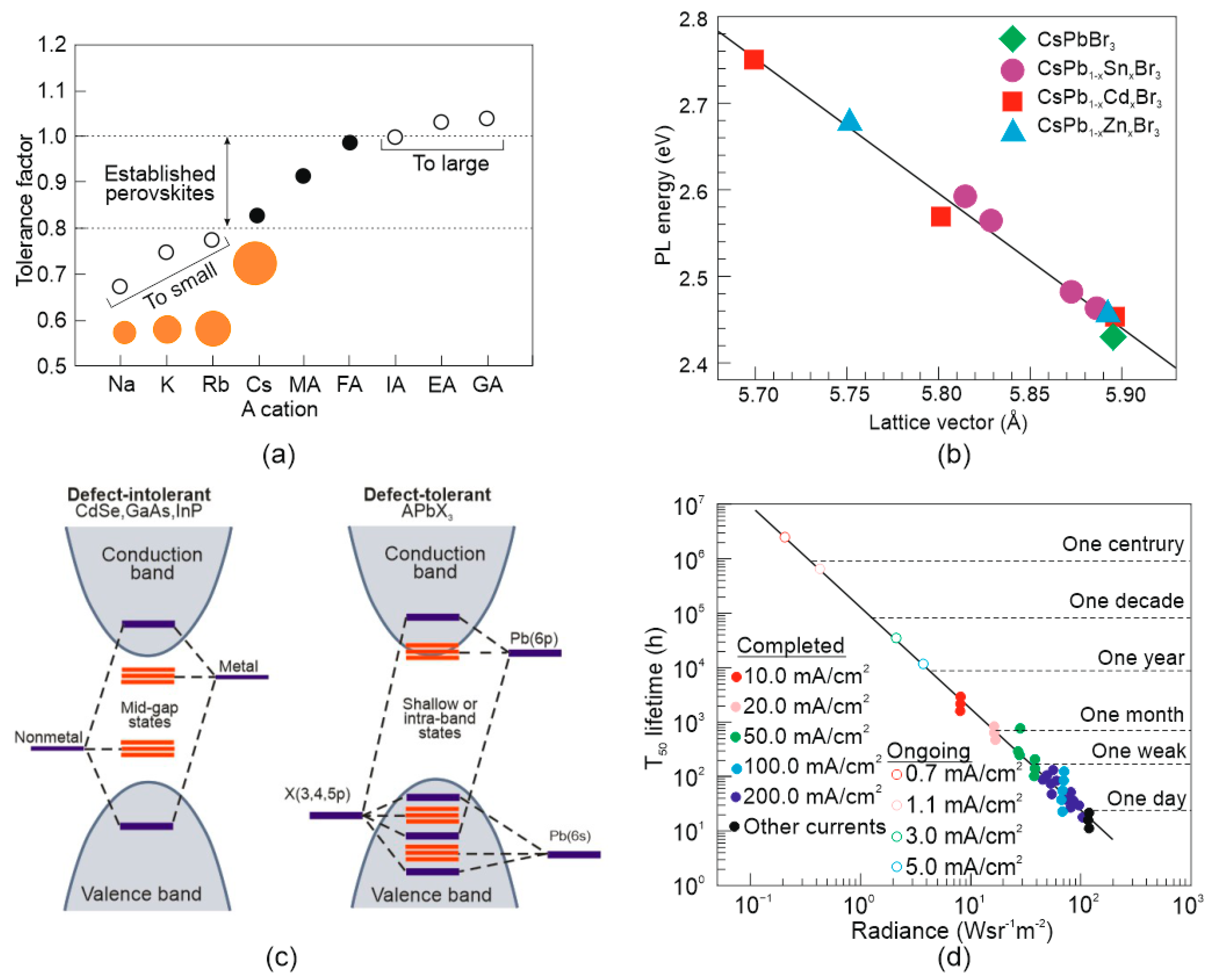
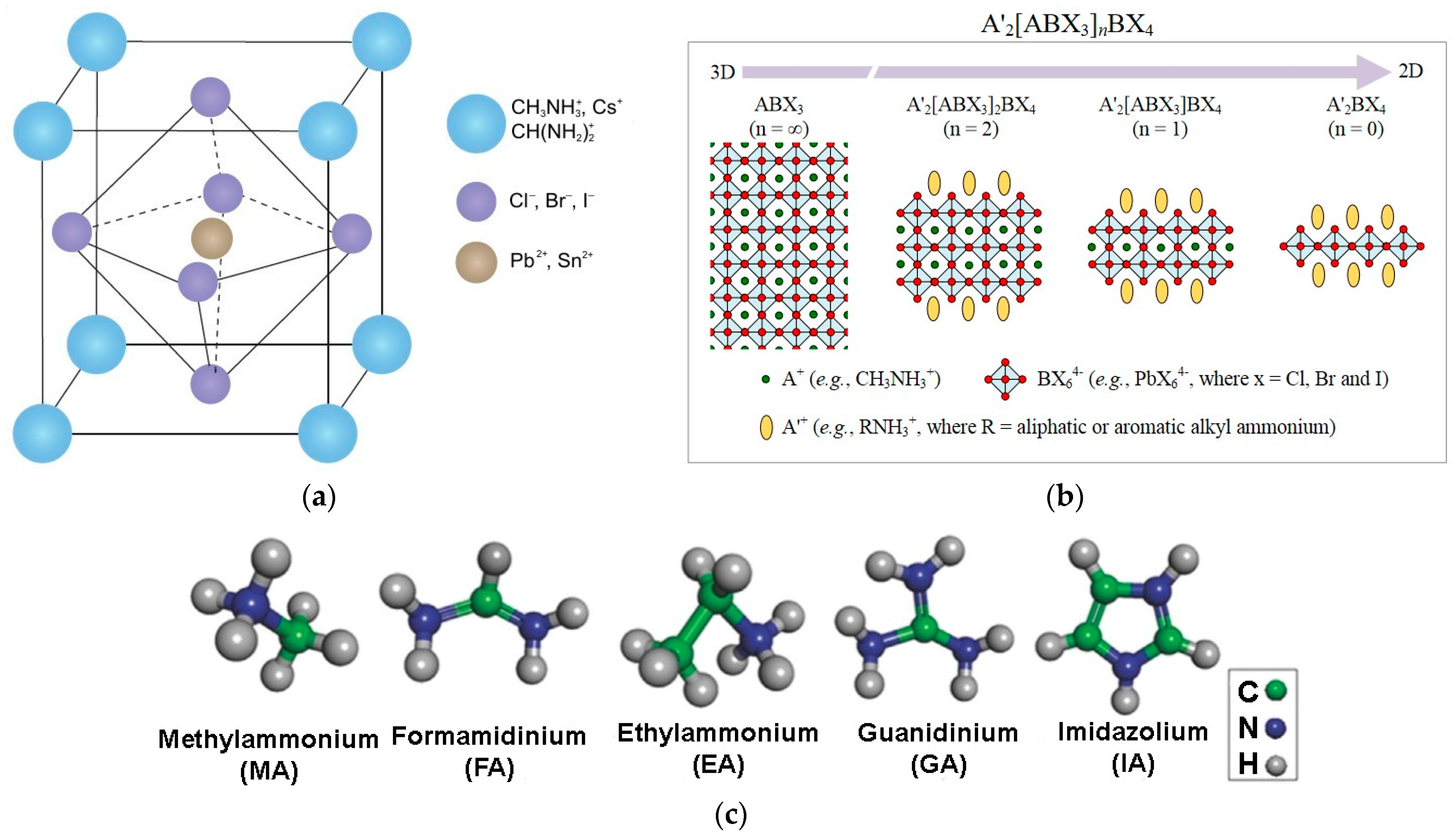
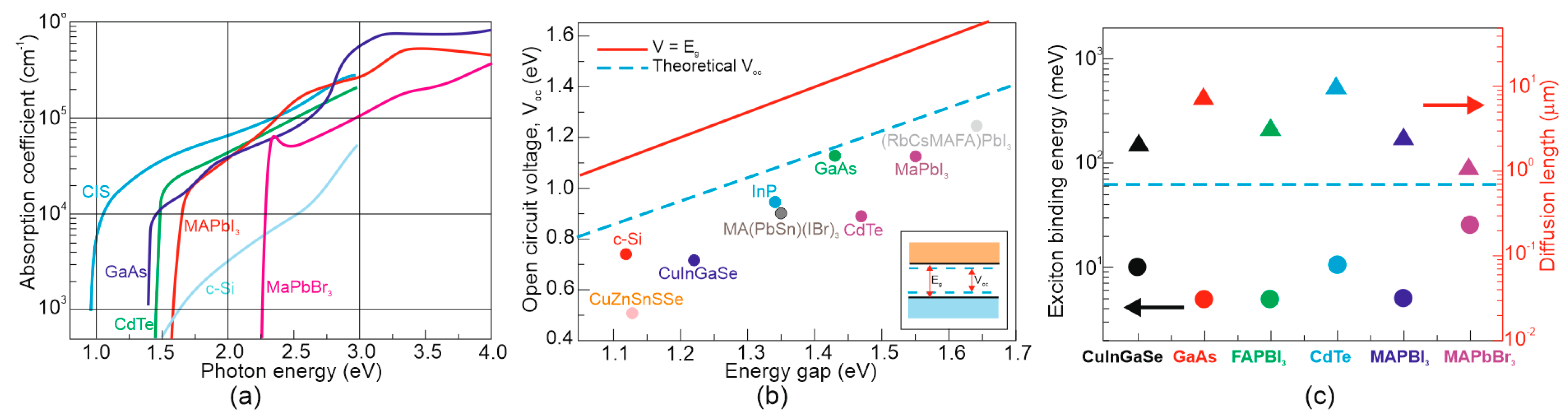
2. Fundamental Properties of Perovskite Materials
3. Performance Limitations of Photodetectors

- Noise;
- The device’s active area and radiation power density;
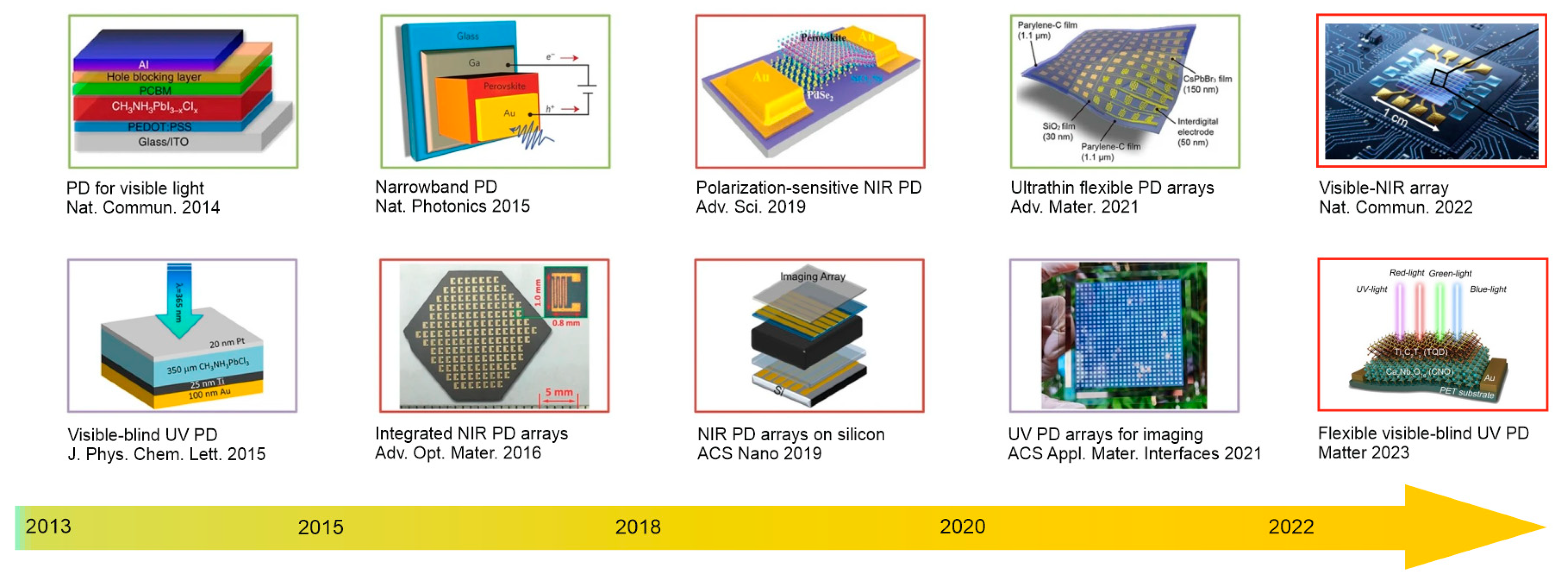
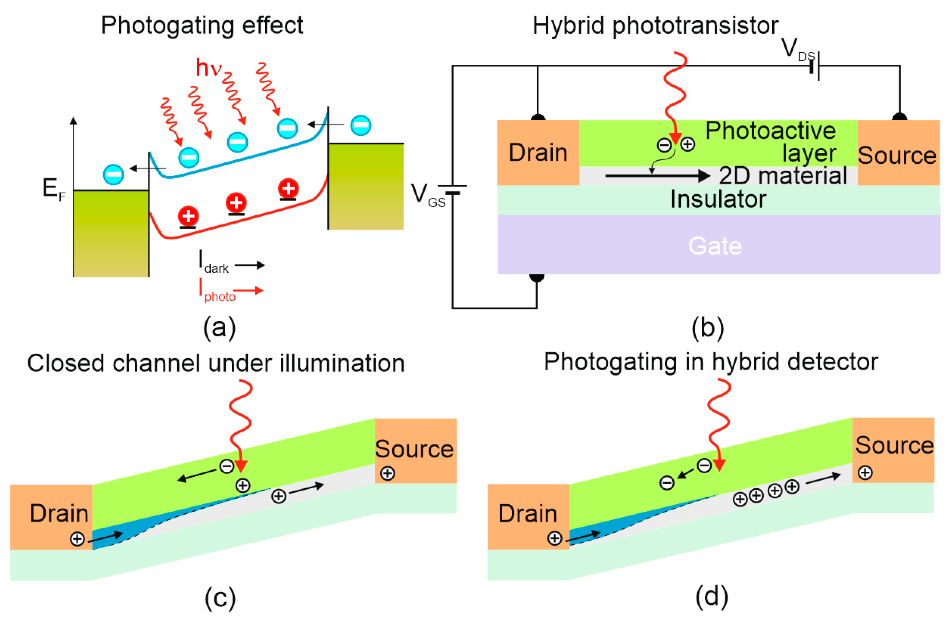
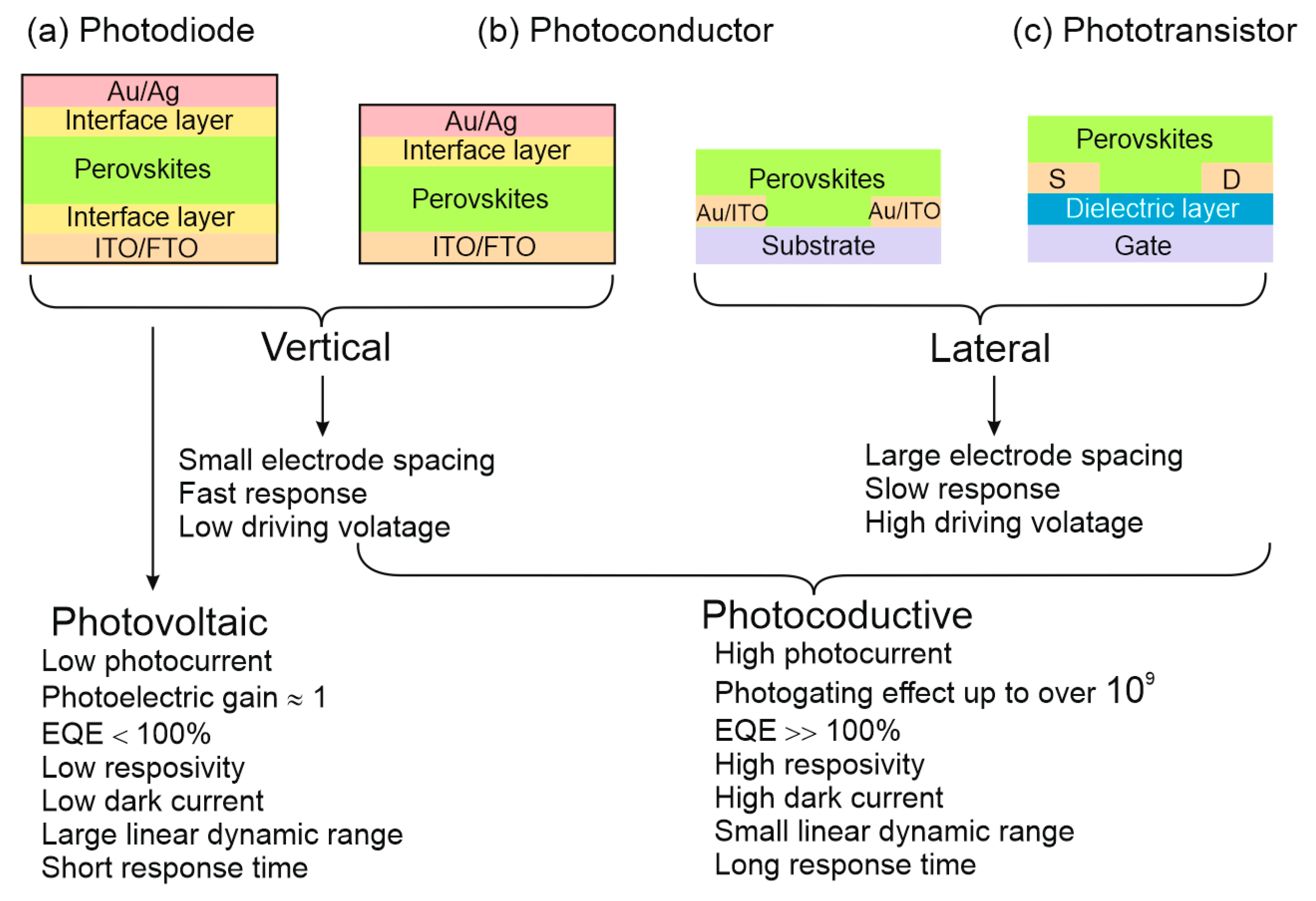
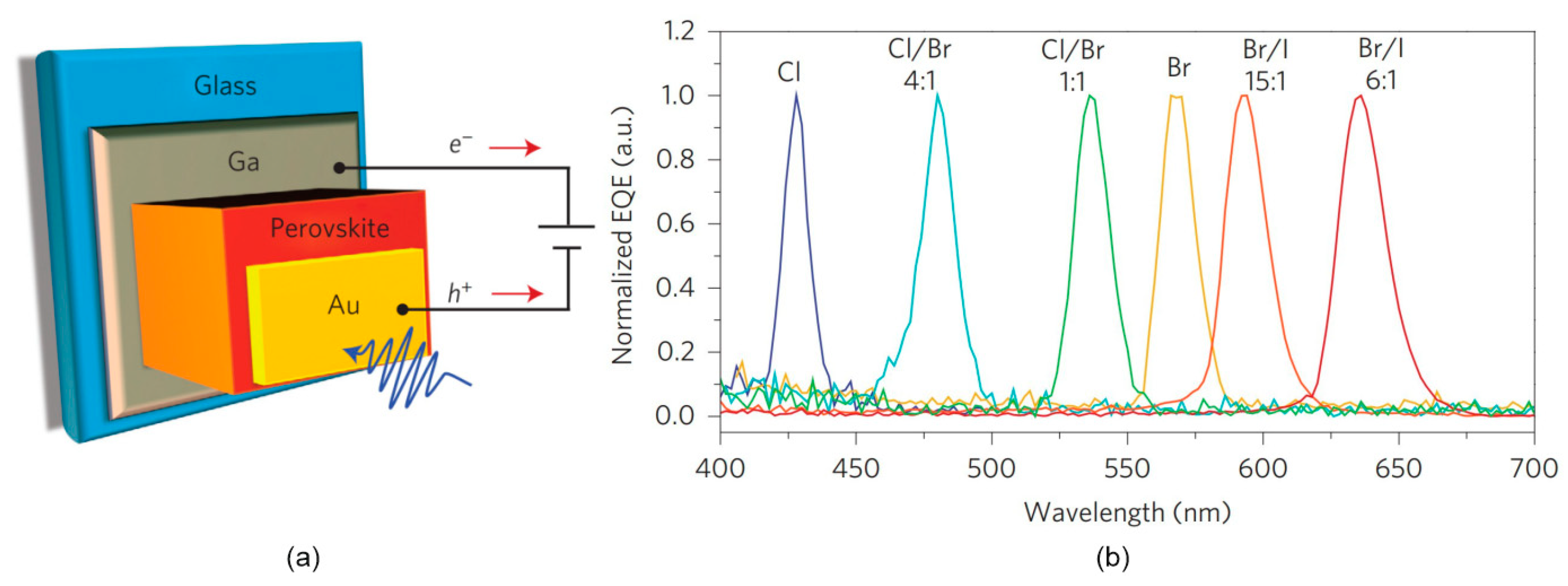
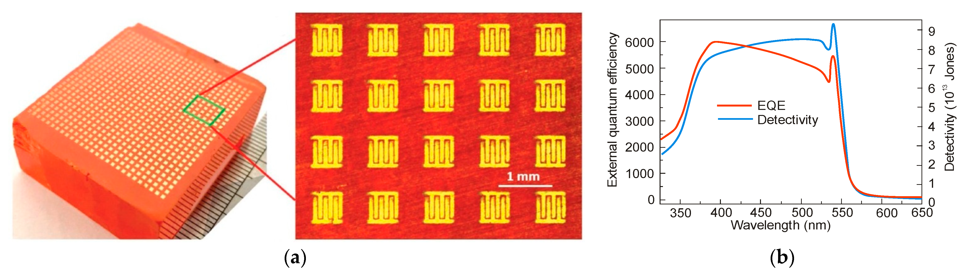
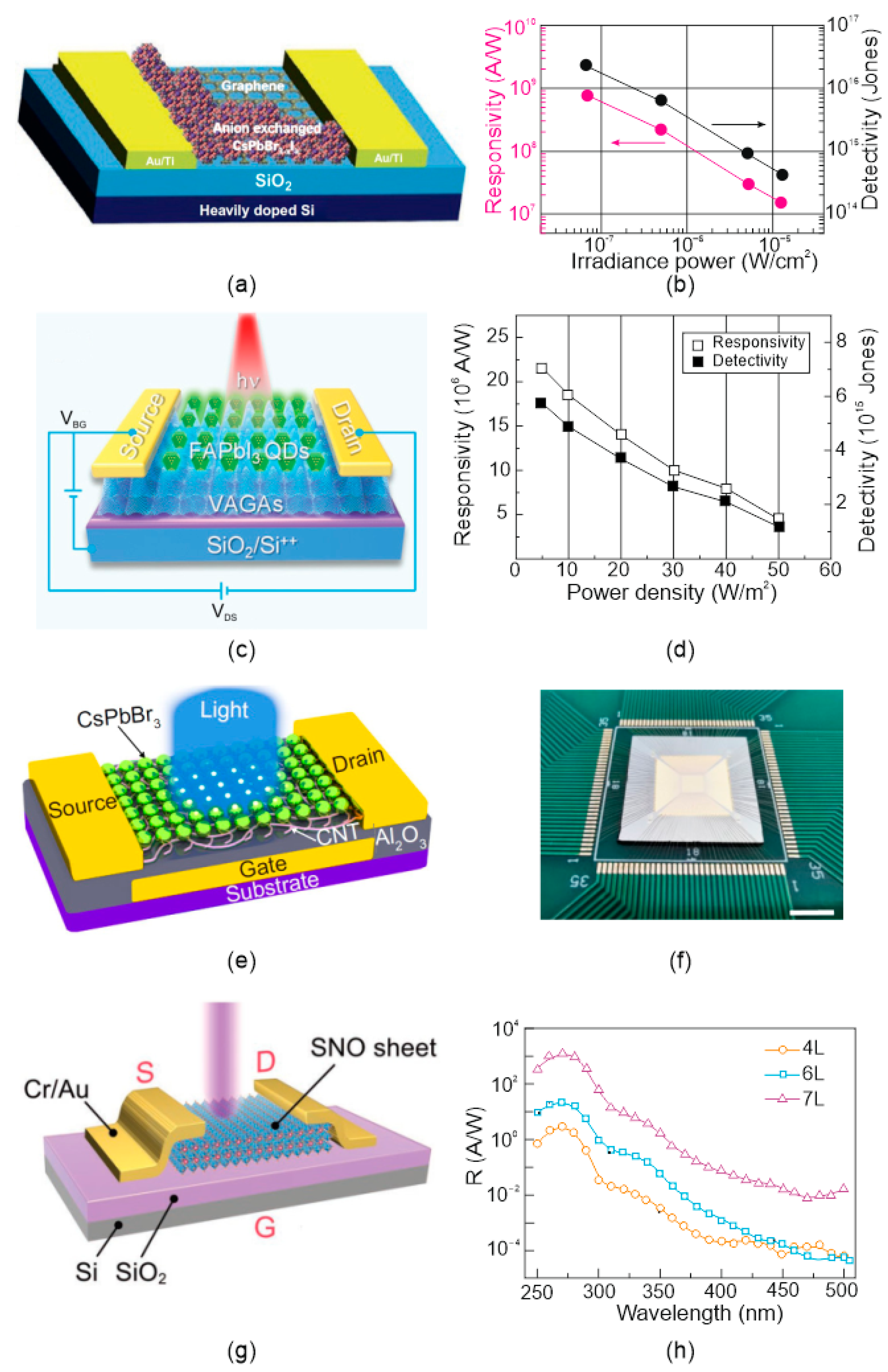
4. Design and Performance of Perovskite Photodetectors
- Electron–hole pairs generation when one type of carrier is trapped by the localized states (nano-particles and defects);
- Electron–hole pair generation in trap states where one type of carrier is transferred to nanostructured materials (generally LDS), whereas the other resides at the same place to modulate the layered materials.
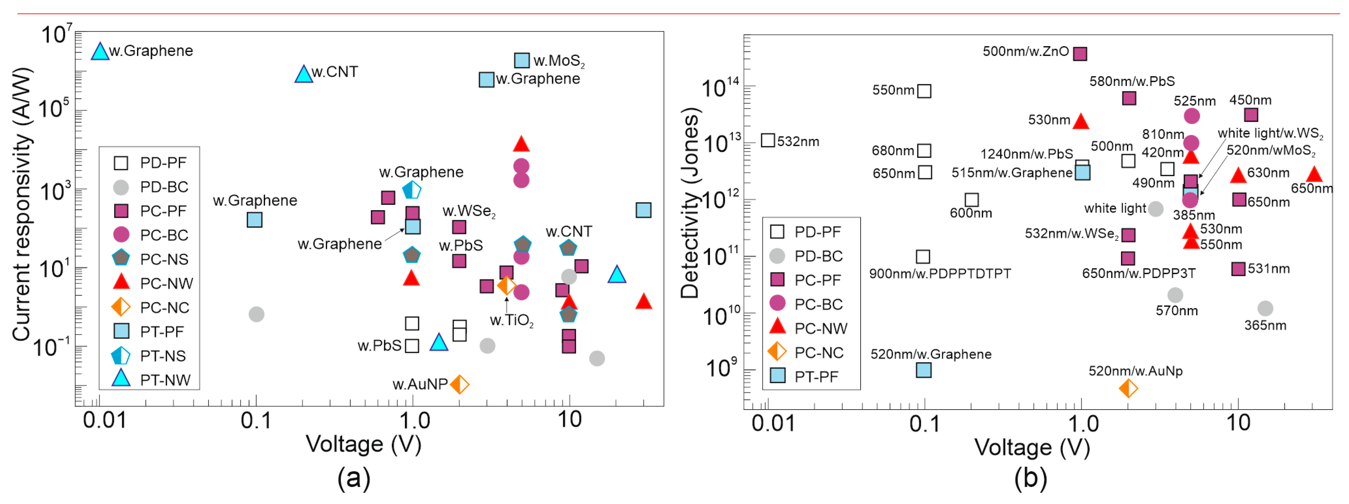
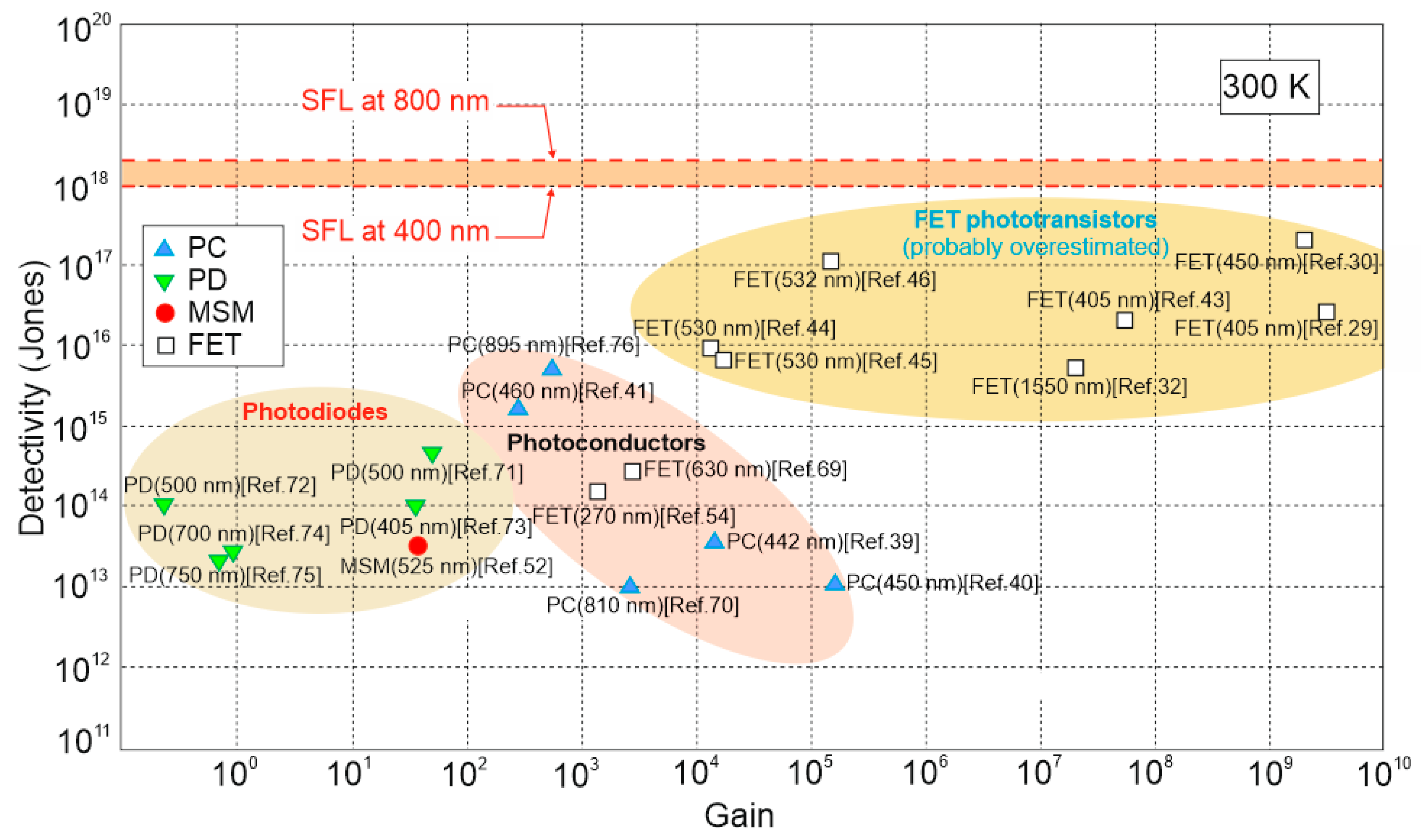
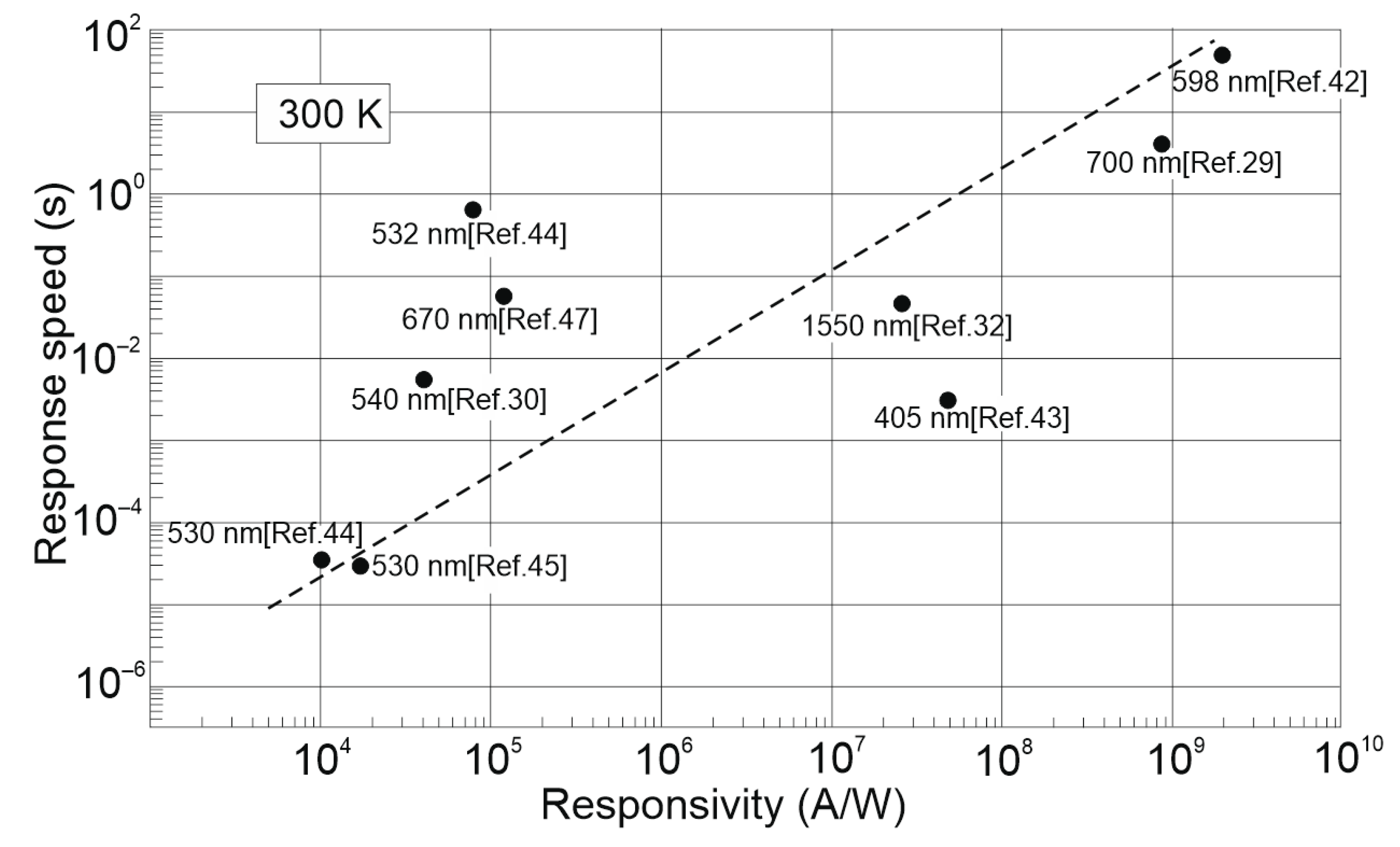
5. Performance Analysis of Perovskite Photodetectors
6. Conclusions
- A wide variety of perovskites have a direct and tuneable energy gap controlled by mixing. Their electronic properties (doping) can also be controlled by the composition. Furthermore, the fabrication methods are relatively simple compared to organic materials (solution-based techniques at low temperatures lead to reasonable energy payback time); however, their physical properties are affected by other factors; e.g., crystallinity, morphology, grain size and processing history.
- The pristine perovskites’ conductivity is relatively low; however, low effective mass allows the carrier mobility to be higher (fewer orders of magnitude) than organic semiconductors. The ultimate mobility limit is driven by the Fröhlich effect, and the carrier’s transport is influenced by the interaction with the electric field of LO phonons.
- Perovskites’ development is mainly triggered by the progressive development of the solid-state perovskite next-generation SCs. Up to now, however, most of the perovskite materials and devices are still fabricated on the laboratory scale.
- The perovskite-based detector’s performance was found to be overestimated in many cases due to: erroneous noise estimates, miscalculations of the device’s active area/light power density, and conflicting bandwidths adopted for the measured noise and sensitivity.
- Several methods including carriers’ trap layers and photogating effect with fast channels may be introduced to increase sensitivity, but the carrier mobility and response time limitations restrict applications (trade-off between response time and sensitivity).
- Generally, the ionic nature perovskites are not that stable as inorganics. In a humid environment, they can drastically change the crystalline structure and composition causing permanent material damage. Effective housing is needed to fully protect the device while long-term stability under extremely harsh operating conditions also remains an issue.
- Toxicity is another issue. So far, lead-based perovskites are the materials that exhibit the best performance; however, lead-free perovskites are gradually being introduced, e.g., bismuth-based and double perovskites.
- another problem is miniaturization, particularly important in imaging arrays. The perovskite synthetization methods are completely different from silicon technology (e.g., conventional lithography, etching techniques) and a long term is necessary to develop the methods comparable with silicon. This question also concerns ROICs of perovskite arrays, where specific design is required (e.g., taking into account large RC sensor times).
Author Contributions
Funding
Data Availability Statement
Conflicts of Interest
References
- Miyasaka, T. Perovskite Photovoltaics and Optoelectronics. From Fundamentals to Advanced Applications; Wiley-VCH GmbH: Weinheim, Germany, 2022. [Google Scholar]
- Ding, L. Perovskite Materials and Devices; Wiley-VCH GmbH: Weinheim, Germany, 2022. [Google Scholar]
- Sutherland, B.R.; Sargen, E.H. Perovskite photonic sources. Nat. Photonics 2016, 10, 295–302. [Google Scholar] [CrossRef]
- Jagielski, J.; Kumar, S.; Yu, W.-Y.; Shih, C.-J. Layer-controlled two-dimensional perovskites: Synthesis and optoelectronics. J. Mater. Chem. C 2017, 5, 5610–5627. [Google Scholar] [CrossRef]
- Goldschmidt, V.M. Die Gesetze der Krystallochemie. Die Naturwissenschaften 1926, 14, 477–485. [Google Scholar] [CrossRef]
- Quan, L.N.; Rand, B.P.; Friend, R.H.; Mhaisalkar, S.G.; Lee, T.-W.; Sargent, E.H. Perovskites for next-generation optical sources. Chem. Rev. 2019, 119, 7444–7477. [Google Scholar] [CrossRef] [PubMed]
- Cho, H.; Kim, Y.-H.; Wolf, C.; Lee, H.-D.; Lee, T.-W. Improving the stability of metal halide perovskite materials and light-emitting diodes. Adv. Mater. 2018, 30, 1704587. [Google Scholar] [CrossRef] [PubMed]
- Stam, W.v.d.; Geuchies, J.J.; Altantzis, T.; Bos, K.H.W.v.d.; Meeldijk, J.D.; Aert, S.V.; Bals, S.; Vanmaekelbergh, D.; Donega, C.d.M. Highly emissive divalent-ion-doped colloidal CsPb1−xMxBr3 perovskite nanocrystals through cation exchange. J. Am. Chem. Soc. 2017, 139, 4087–4097. [Google Scholar] [CrossRef]
- Kovalenko, M.V.; Protesescu, L.; Bodnarchuk, M.I. Properties and potential optoelectronic applications of lead halide perovskite nanocrystals. Science 2017, 358, 745–750. [Google Scholar] [CrossRef] [PubMed]
- Guo, B.; Lai, R.; Jiang, S.; Zhou, L.; Ren, Z.; Lian, Y.; Li, P.; Cao, X.; Xing, S.; Wang, Y.; et al. Ultrastable near-infrared perovskite light emitting diodes. Nat. Photonics 2022, 16, 637–643. [Google Scholar] [CrossRef]
- Wang, Y.; Gao, M.-L.; Wu, J.-L.; Zhang, X.-W. Metal halide perovskite photodetectors: Material features and device engineering. Chin. Phys. B 2019, 28, 018502. [Google Scholar] [CrossRef]
- Conings, B.; Drijkoningen, J.; Gauquelin, N.; Babayigit, A.; D’Haen, J.; D’Olieslaeger, L.; Ethirajan, A.; Verbeeck, J.; Manca, J.J.; Mosconi, E.; et al. Intrinsic thermal instability of methylammonium lead trihalide perovskite. Adv. Energy Mater. 2015, 5, 1500477. [Google Scholar] [CrossRef]
- Jeon, N.J.; Noh, J.H.; Yang, W.S.; Kim, Y.C.; Ryu, S.; Seo, J.; Seok, S.I. Compositional engineering of perovskite materials for high-performance solar cell. Nature 2015, 517, 476–480. [Google Scholar] [CrossRef] [PubMed]
- Polman, A.; Knight, M.; Garnett, E.C.; Ehrler, B.; Sinke, W.C. Photovoltaic materials—Present efficiencies and future challenges. Science 2016, 352, aad4424. [Google Scholar] [CrossRef] [PubMed]
- Rajagopal, A.; Yao, K.; Jen, A.K.-Y. Toward perovskite solar cell commercialization: A perspective and research roadmap based on interfacial engineering. Adv. Mater. 2018, 30, 1800455. [Google Scholar] [CrossRef] [PubMed]
- Roy, P.; Ghosh, A.; Barclay, F.; Khare, A.; Cuce, E. Perovskite solar cells: A review of the recent advances. Coatings 2022, 12, 1089. [Google Scholar] [CrossRef]
- Miyata, A.; Mitioglu, A.; Plochocka, P.; Portugall, O.; Wang, J.T.-W.; Stranks, S.D.; Snaith, H.; Nicholas, R. Direct measurement of the exciton binding energy and effective masses for charge carriers in organic-inorganic tri-halide perovskite. Nat. Phys. 2015, 11, 582–587. [Google Scholar] [CrossRef]
- Li, C.; Sun, H.; Gan, S.; Dou, D.; Li, L. Perovskite single crystals: Physical properties and optoelectronic applications. Mater. Futures 2023, 2, 042101. [Google Scholar] [CrossRef]
- Li, G.; Wang, Y.; Huang, L.; Sun, W. Research progress of high-sensitivity perovskite photodetectors: A review of photodetectors: Noise, structure, and materials. ACS Appl. Electron. Mater. 2022, 4, 1485–1505. [Google Scholar] [CrossRef]
- Herz, L.M. Charge-carrier mobilities in metal halide perovskites: Fundamental mechanisms and limits. ACS Energy Lett. 2017, 2, 1539–1548. [Google Scholar] [CrossRef]
- Koh, T.M.; Fu, K.; Fang, Y.; Chen, S.; Sum, T.C.; Mathews, N.; Mhaisalkar, S.G.; Boix, P.P.; Baikie, T. Formamidinium-containing metal-halide: An alternative material for near-IR absorption perovskite solar cells. J. Phys. Chem. C 2013, 118, 16458–16462. [Google Scholar] [CrossRef]
- Bielecki, Z.; Achtenberg, K.; Kopytko, M.; Mikołajczyk, J.; Wojtas, J.; Rogalski, A. Review of photodetectors characterization methods. Bull. Pol. Acad. Sci. Tech. Sci. 2022, 70, e140534. [Google Scholar] [CrossRef]
- Fang, H.; Hu, W. Photogating in low dimensional photodetectors. Adv. Sci. 2017, 4, 170323. [Google Scholar] [CrossRef] [PubMed]
- Kruse, P.W. The photon detection process. In Optical and Infrared Detectors; Keyes, R.J., Ed.; Springer: Berlin/Heidelberg, Germany, 1977; pp. 5–69. [Google Scholar]
- Kingston, R.H. Detection of Optical and Infrared Radiation; Wiley: New York, NY, USA, 1983. [Google Scholar]
- Dereniak, E.L.; Boremen, G.D. Infrared Detectors and Systems; Wiley: New York, NY, USA, 1996. [Google Scholar]
- Li, X.; Zhu, C.; Zhu, X.; Xu, Z.; Zhuang, X.; Ji, X.; Yan, F. Background limited ultraviolet photodetectors of solar-blind ultraviolet detection. Appl. Phys. Lett. 2013, 103, 171110. [Google Scholar] [CrossRef]
- Wang, H.; Kim, D.H. Perovskite-based photodetectors: Materials and devices. Chem. Soc. Rev. 2017, 46, 5204–5236. [Google Scholar] [CrossRef] [PubMed]
- Kwak, D.H.; Lim, D.H.; Ra, H.S.; Ramasamy, P.; Lee, J.S. High performance hybrid graphene-CsPbBr3-xIx perovskite nano-crystal photodetector. RSC Adv. 2016, 6, 65252–65256. [Google Scholar] [CrossRef]
- Yu, Y.; Zhang, Y.; Jin, L.; Chen, Z.; Li, Y.; Li, Q.; Cao, M.; Che, Y.; Yao, J. Solution-possessed vertical photodetectors based on composition dependent cesium lead halide (CsPbX3, X = Cl, Br, and I) perovskite quantum dots. Proc. SPIE 2019, 10914, 1091419. [Google Scholar]
- Chang, P.-H.; Liu, S.-Y.; Lan, Y.-B.; Tsai, Y.-C.; You, X.-Q.; Li, C.-S.; Huang, K.-Y.; Chou, A.-S.; Cheng, T.-C.; Wang, J.-K.; et al. Ultrahigh responsivity and detectivity graphene-perovskite hybrid phototransistors by sequential vapor deposition. Sci. Rep. 2017, 7, 46281. [Google Scholar] [CrossRef] [PubMed]
- Feng, X.; He, Z.; Zhu, W.; Zhao, M.; Liu, Z.; Yang, S.; Tang, S.; Guo, Q.; Jin, Z.; Chen, D.; et al. Perovskite quantum dots integrated with vertically aligned graphene toward ambipolar multifunctional photodetectors. J. Mater. Chem. C 2021, 9, 609–619. [Google Scholar] [CrossRef]
- Bianconi, S.; Lauhon, L.J.; Mohseni, H. Exaggerated sensitivity in photodetectors with internal gain. Nat. Photonics 2021, 15, 714. [Google Scholar] [CrossRef]
- Rogalski, A. Detectivities of WS2/HfS2 heterojunctions. Nat. Nanotechnol. 2022, 17, 217–219. [Google Scholar] [CrossRef]
- Rogalski, A. Overestimating the performance of photon ultraviolet detectors. IEEE Electron Device Lett. 2023, 44, 805–808. [Google Scholar] [CrossRef]
- Wang, F.; Zhang, T.; Xie, R.; Wang, Z.; Hu, W. How to characterize figures of merit two-dimensional photodetectors. Nat. Commun. 2023, 14, 2224. [Google Scholar] [CrossRef] [PubMed]
- Zhang, L.; Mei, L.; Wang, K.; Lv, Y.; Zhang, S.; Lian, Y.; Liu, X.; Ma, Z.; Xiao, G.; Liu, Q.; et al. Advances in the application of perovskite materials. Nano-Micro Lett. 2023, 15, 177. [Google Scholar] [CrossRef] [PubMed]
- Ghosh, J.; Girl, P.K. Recent advances in perovskite/2D materials based hybrid photodetectors. J. Phys. Mater. 2021, 4, 032008. [Google Scholar] [CrossRef]
- Chen, Y.; Chen, G.; Zhou, Z.; Li, X.; Ma, P.; Li, L.; Yin, W.; Zeng, H.; Zou, G. Amplifying surface energy difference toward anisotropic growth of all-inorganic perovskite single-crystal wires for highly sensitive photodetector. Adv. Funct. Mater. 2021, 31, 2101966. [Google Scholar] [CrossRef]
- Yang, B.; Zhang, F.; Chen, J.; Yang, S.; Xia, X.; Pullerits, T.; Deng, W.; Han, K. Ultrasensitive and fast all-inorganic perovskite-based photodetector via fast carrier diffusion. Adv. Mater. 2017, 29, 1703758. [Google Scholar] [CrossRef] [PubMed]
- Liu, Y.; Zhang, Y.; Yang, Z.; Ye, H.; Feng, J.; Xu, Z.; Zhang, X.; Munir, R.; Liu, J.; Zuo, P.; et al. Multi-inch single-crystalline perovskite membrane for high-detectivity flexible photosensors. Nat. Commun. 2018, 9, 5302. [Google Scholar] [CrossRef] [PubMed]
- Xie, C.; You, P.; Liu, Z.; Li, L.; Yan, F. Ultrasensitive broadband phototransistors based on perovskite/organic-semiconductor vertical heterojunctions. Light Sci. Appl. 2017, 6, e17023. [Google Scholar] [CrossRef] [PubMed]
- Zhu, Q.-B.; Li, B.; Yang, D.-D.; Liu, C.; Feng, S.; Chen, M.-L.; Sun, Y.; Tian, Y.-N.; Su, X.; Wang, X.-M.; et al. A flexible ultrasensitive optoelectronic sensor array for neuromorphic vision systems. Nat. Commun. 2021, 12, 1798. [Google Scholar] [CrossRef]
- Zhao, Y.; Qiu, Y.; Gao, H.; Feng, J.; Chen, G.; Jiang, L.; Wu, Y. Layered-perovskite nanowires with long-range orientational order for ultrasensitive photodetectors. Adv. Mater. 2020, 32, 1905298. [Google Scholar] [CrossRef]
- Feng, J.; Gong, C.; Gao, H.; Wen, W.; Gong, Y.; Jiang, X.; Zhang, B.; Wu, Y.; Wu, Y.; Fu, H.; et al. Single-crystalline layered metal-halide perovskite nanowires for ultrasensitive photodetectors. Nat. Electron. 2018, 1, 404–410. [Google Scholar] [CrossRef]
- Zhu, H.; Liu, A.; Luque, H.L.; Sun, H.; Ji, D.; Noh, Y.Y. Perovskite and conjugated polymer wrapped semiconducting carbon nanotube hybrid films for high-performance transistors and phototransistors. ACS Nano 2019, 13, 3971–3981. [Google Scholar] [CrossRef]
- Pan, R.; Li, H.; Wang, J.; Jin, X.; Li, Q.; Wu, Z.; Gou, J.; Jiang, Y.; Song, Y. High-responsivity photodetectors based on formamidinium lead halide perovskite quantum dot-graphene hybrid. Particle 2018, 35, 1700304. [Google Scholar] [CrossRef]
- Wu, H.; Si, H.; Zhang, Z.; Kang, Z.; Wu, P.; Zhou, L.; Zhang, S.; Zhang, Z.; Liao, Q.; Zhang, Y. All-inorganic perovskite quantum dot-monolayer MoS2 mixed-dimensional van der Waals heterostructure for ultrasensitive photodetector. Adv. Sci. 2018, 5, 1801219. [Google Scholar] [CrossRef]
- Fang, Y.; Dong, Q.; Shao, Y.; Yuan, Y.; Huang, J. Highly narrowband perovskite single-crystal photodetectors enabled by surface-charge recombination. Nat. Photon. 2015, 9, 679–686. [Google Scholar] [CrossRef]
- Lin, Q.; Armin, A.; Burn, P.L.; Meredith, P. Filterless narrowband visible photodetectors. Nat. Photon. 2015, 9, 687–694. [Google Scholar] [CrossRef]
- Dou, Y.; Yang, Y.M.; You, J.; Hong, Z.; Chang, W.H.; Li, G.; Yang, Y. Solution-processed hybrid perovskite photodetectors with high detectivity. Nat. Commun. 2014, 5, 5404. [Google Scholar] [CrossRef]
- Liu, Y.; Zhang, Y.; Zhao, K.; Yang, Z.; Feng, J.; Zhang, X.; Wang, K.; Meng, L.; Ye, H.; Liu, M.; et al. A 1300 mm2 ultrahigh-performance digital imaging assembly using high-quality perovskite single crystals. Adv. Mater. 2018, 30, 1707314. [Google Scholar] [CrossRef]
- Rogalski, A. 2D Materials for Infrared and Terahertz Detectors; CRC Press: Boca Raton, FL, USA, 2022. [Google Scholar]
- Li, S.; Zhang, Y.; Yang, W.; Liu, H.; Fang, X. 2D perovskite Sr2Nb3O10 for high-performance UV photodetectors. Adv. Mater. 2019, 32, 1905443. [Google Scholar] [CrossRef]
- Zhang, X.; Liu, X.; Huang, Y.; Sun, B.; Liu, Z.; Liao, G.; Shi, T. Review on flexible perovskite photodetector: Processing and applications. Front. Mech. Eng. 2023, 18, 33. [Google Scholar] [CrossRef]
- Leung, S.-F.; Ho, K.-T.; Kung, P.-K.; Hsiao, V.K.S.; Alshareef, H.N.; Wang, Z.L.; He, J.-H. A self-powered and flexible organometallic halide perovskite photodetector with very high detectivity. Adv. Mater. 2018, 30, 1704611. [Google Scholar] [CrossRef]
- Sheng, X.; Li, Y.; Xia, M.; Shi, E. Quasi-2D halide perovskite crystals and their optoelectronic applications. J. Mater. Chem. A 2022, 10, 19169–19183. [Google Scholar] [CrossRef]
- Ma, C.; Shi, Y.; Hu, W.; Chiu, M.-H.; Liu, Z.; Bera, A.; Li, F.; Wang, H.; Li, L.-J.; Wu, T. Heterostructured WS2/CH3NH3PbI3 photoconductors with suppressed dark current and enhanced photodetectivity. Adv. Mater. 2016, 28, 3683–3689. [Google Scholar] [CrossRef] [PubMed]
- Du, S.; Li, G.; Cao, X.; Wang, Y.; Lu, H.; Zhang, S.; Liu, C.; Zhou, H. Oxide semiconductor phototransistor with organolead trihalide perovskite light absorber. Adv. Electron. Mater. 2017, 3, 1600325. [Google Scholar] [CrossRef]
- Chen, Z.; Kang, Z.; Rao, C.; Cheng, Y.; Liu, N.; Zhang, Z.; Li, L.; Gao, Y. Improving performance of hybrid graphene–perovskite photodetector by a scratch channel. Adv. Electron. Mater. 2019, 5, 1900168. [Google Scholar] [CrossRef]
- Che, Y.; Cao, Y.X.; Zhang, Y.; Yao, J. High performance CsPbBr3 perovskite nanocrystal vertical phototransistor with graphene electrode. Opt. Mater. 2020, 100, 109664. [Google Scholar] [CrossRef]
- Li, J.; Yuan, S.; Tang, G.; Li, G.; Liu, D.; Li, J.; Hu, X.; Liu, Y.; Li, J.; Yang, Z.; et al. High-performance, self-powered photodetectors based on perovskite and graphene. ACS Appl. Mater. Interfaces 2017, 9, 42779–42787. [Google Scholar] [CrossRef] [PubMed]
- Chen, J.; Jing, Q.; Xu, F.; Lu, Z.; Lu, Y. High-sensitivity optical-fiber-compatible photodetector with an integrated CsPbBr3–graphene hybrid structure. Optica 2017, 4, 835–838. [Google Scholar] [CrossRef]
- Surendran, A.; Yu, X.; Begum, R.; Tao, Y.; Wang, Q.J.; Leong, W.L. All inorganic mixed halide perovskite nanocrystal-graphene hybrid photodetector: From ultrahigh gain to photostability. ACS Appl. Mater. Interfaces 2019, 11, 27064–27072. [Google Scholar] [CrossRef] [PubMed]
- Zhang, M.; Zhang, F.; Wang, Y.; Zhu, L.; Hu, Y.; Lou, Z.; Hou, Y.; Teng, F. High-performance photodiode-type photodetectors based on polycrystalline formamidinium lead iodide perovskite thin films. Sci. Rep. 2018, 8, 11157. [Google Scholar] [CrossRef]
- Zou, Y.; Zou, T.; Zhao, C.; Wang, B.; Xing, J.; Yu, Z.; Cheng, J.; Xin, W.; Yang, J.; Yu, W.; et al. A highly sensitive single crystal perovskite–graphene hybrid vertical photodetector. Small 2020, 16, 2000733. [Google Scholar] [CrossRef]
- Bessonov, A.A.; Allen, M.; Liu, Y.; Malik, S.; Bottomley, J.; Rushton, A.; Medina-Salazar, I.; Voutilainen, M.; Kallioinen, S.; Colli, A.; et al. Compound quantum dot–perovskite optical absorbers on graphene enhancing short-wave infrared photodetection. ACS Nano 2017, 11, 5547–5557. [Google Scholar] [CrossRef]
- Lee, Y.; Kwon, J.; Hwang, E.; Ra, C.H.; Yoo, W.J.; Ahn, J.H.; Park, J.H.; Cho, J.H. High-performance perovskite-graphene hybrid photodetector. Adv. Mater. 2015, 27, 41–46. [Google Scholar] [CrossRef]
- Chen, G.; Feng, J.; Gao, H.; Zhao, Y.; Pi, Y.; Jiang, X.; Wu, Y.; Jiang, L. Stable α-CsPbI3 perovskite nanowire arrays with preferential crystallographic orientation for highly sensitive photodetectors. Adv. Funct. Mater. 2019, 29, 1808741. [Google Scholar] [CrossRef]
- Saidaminov, M.I.; Haque, M.A.; Savoie, M.; Abdelhady, A.L.; Cho, N.; Dursun, I.; Buttner, U.; Alarousu, E.; Wu, T.; Bakr, O.M. Perovskite photodetectors operating in both narrowband and broadband regimes. Adv. Mater. 2016, 28, 8144–8149. [Google Scholar] [CrossRef] [PubMed]
- Yu, J.; Chen, X.; Wang, Y.; Zhou, H.; Xue, M.; Xu, Y.; Li, Z.; Ye, C.; Zhang, J.; van Aken, P.A.; et al. A high-performance self-powered broadband photodetector based on a CH3NH3PbI3 perovskite/ZnO nanorod array heterostructure. J. Mater. Chem. C 2016, 4, 7302–7308. [Google Scholar] [CrossRef]
- Tian, C.; Wang, F.; Wang, Y.; Yang, Z.; Chen, X.; Mei, X.; Liu, H.; Zhao, D. Chemical vapor deposition method grown all-inorganic perovskite microcrystals for self-powered photodetectors. ACS Appl. Mater. Interfaces 2019, 11, 15804–15812. [Google Scholar] [CrossRef]
- Shen, K.; Xu, H.; Li, X.; Guo, J.; Sathasivam, S.; Wang, M.; Ren, A.; Choy, K.L.; Parkin, I.P.; Guo, Z.; et al. Flexible and self-powered photodetector arrays based on all-inorganic CsPbBr3 quantum dots. Adv. Mater. 2020, 32, 2000004. [Google Scholar] [CrossRef]
- Cao, F.; Meng, L.; Wang, M.; Tian, W.; Li, L. Gradient Energy band driven high-performance self-powered perovskite/CdS photodetector. Adv. Mater. 2019, 31, 1806725. [Google Scholar] [CrossRef]
- Lee, D.S.; Heo, J.H.; Park, J.K.; Kim, B.W.; Lee, H.J.; Song, Y.M.; Im, S.H. Enhanced weak-light detection of perovskite photodetectors through perovskite/hole-transport material interface treatment. ACS Appl. Mater. Interfaces 2021, 13, 16775. [Google Scholar] [CrossRef]
- Xin, J.; Wang, Q.; Li, J.; Wang, K.; Deng, W.; Jin, J.; Peng, M.; Fang, M.; Qu, J.; Wang, H. Planar visible–near infrared photodetectors based on organic–inorganic hybrid perovskite single crystal bulks. J. Phys. D Appl. Phys. 2020, 53, 414003. [Google Scholar] [CrossRef]


| Parameter | Value |
|---|---|
| Energy gap | 1.5–2.5 eV |
| Absorption coefficient | 105 cm−1 |
| Exciton binding energy | <10 meV |
| Crystallization energy barrier | 56.6–97.3 kJ/mol |
| Charge carrier lifetime | Greater than 300 ns |
| PL quantum efficiency (QE) | 70% |
| Carrier mobility | 800 cm2/Vs |
| Relative permittivity | 3 |
| Exciton | Wannier type exciton |
| Trap-state density | 1010 cm−3 (single crystals) 1015–1017 cm−3 (polycrystals) |
| Materials | Mobility (cm2/Vs) | Carrier Lifetime (ns) | Diffusion Length (mm) | Trap Density (cm–3) | Carrier Concen (cm−3) |
|---|---|---|---|---|---|
| MAPbCl3 (ITC) (1) | For hole: 42 ± 9 (SCLC) (4) | τs = 83 τb = 662 (TA) (6) | 3.0–8.5 | For hole: 3.1 × 10¹⁰ (SCLC) | 4 × 10⁹ |
| MAPbBr3 (ITC) | For hole: 60 (SCLC and Hall effect) | 242 | A few micrometers | For hole: 1.6 × 10¹¹ (SCLC) | For hole: 1011 (Hall effect) |
| MAPbBr3 (AVC) (2) | 115 (ToF) (5) 20–60 (Hall effect) 38 ± 5 (SCLC) | τs = 74 ± 5 τb = 978 ± 22 (TA) τs = 41 ± 2 τb = 357 ± 11 (TRPL) (7) | 3–17 | (5.80 ± 0.6) × 109 (SCLC) | For hole: 5 × 10⁹ 5 × 10¹⁰ (Hall effect) |
| MAPbI3 (ITC) | For hole: 67.2 ± 7.3 (SCLC) | τs = 18 ± 6 τb = 570 ± 69 (TA) | 1.8–10.0 | For hole: (1.4 ± 0.2) × 1010 (SCLC) | — |
| MAPbI3 (TSSG) (3) | For hole: 105 ± 35 (Hall effect); 164 ± 25 (SCLC) For electron: 24.8 ± 4.1 (SCLC); 24.0 ± 6.8 (ToF) | Under 1 sun: 8.2 × 10⁴ (TPV) (8) 9.5 × 10⁴ (IS) (9) Under 0.1 sun: 2.3 × 10⁵ (TPV) 2.0 × 10⁵ (IS) | For hole: 175 ± 25 | For hole: 3.6 × 10¹⁰ For electron: 4.5 × 10¹⁰ (SCLC) | For hole: (9 ± 2) × 109 (Hall effect) |
| MAPbI3 | 68 (SCLC) | τs = 94 τb = 493 (TRPL) | 4.0 | — | — |
| a-FAPbI3 (ITC) | 4.4 (SCLC) 1.07 ± 0.25 (ToF) | τs = 32 τb = 484 (TRPL) | 0.5–2.2 | 6.2 × 10¹¹ (SCLC) | 1.5 × 10¹¹ |
| FAPbI3 | 41 (SCLC) | τs = 79 τb = 1393 (TRPL) | 2.9 | — | — |
| Parametr | PC Detector | PV Detector | Schematic Figures |
|---|---|---|---|
| Gain (g) | (1) | (for APD >> 1) (2) | 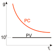 |
| Responsivity (R) | (3) | (4) | 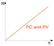 |
| Noise | (5) | (6) |  |
| Noise equivalent power (NEP) | (7) | (8) | 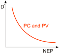 |
| Detectivity (D*) | (9) | (10) | |
| BLIP detectivity |  | ||
| SFL detectivity | |||
| Linear dynamic range (LDR) | , where a ≈ 1 | , where a ≈ 1 |  |
| Device/Materials | Morphology | Spectral Region [nm] | R [A/W] @ Vbias [V], (l [nm], P [W/cm2]) | D* [Jones] @ Vbias [V] (l [nm], P [mW/cm2]) | LDR [dB] | Rise Time/Fall Time | Ref. |
|---|---|---|---|---|---|---|---|
| Photodiodes | |||||||
| PD/MAPbI3−xClx | PF | 300–800 | - | 8 × 10¹³ @ −0.1 (550, 1) | >100 | 180 ns/160 ns | [11] |
| PD/MAPbI3 | PF | 300–800 | - | ~3 × 10¹² @ 0 (700) | ~170 | 1.7 μs/1.0 μs | [11] |
| PD/MAPbCl3 | SCR | 365 | ~0.05 @ −15 (365, 1) | 1.2 × 10¹⁰ | - | 24 ms/62 ms | [11] |
| PD/MAPbBr3 | SCR | ~555–585 | - | 2 × 10¹⁰ @ 4 (570) | - | ~1.6 ms | [11] |
| Photoconductors | |||||||
| PC/MAPbBr3 | SCR | 380–600 | >4000 @ 5 (525) | >3 × 10¹³ | - | ~25 μs/25 μs | [39] |
| PC/MAPb(BrxI1−x)3 | SCR | 405–710 | 2.36 A/W @ 2 (460) | 1.15 × 10¹² | - | 3.4 mqs/3.6 ms | [11] |
| PC/MAPbI3 | NWs | 400-750 | 4.95 @ 1 (530, 2 n) | 2 × 10¹³ | - | <0.1 ms | [11] |
| PC/Csx(MA)1−xPbI3 | NW | 530 | 23 @ 5 (530, 4.5 m) | 2.5 × 10¹¹ | - | - | [11] |
| PC/MAPbI3 | NW | 370–780 | 12500 @ 5 (550, 42 m) | 1.73 × 10¹¹ | 114 | 0.34 μs/0.42 μs | [11] |
| PC/CsPbBr3+Au nanoparticles | NC | 300–550 | ~0.01 @ 2 (520) | 4.56 × 10⁸ | - | 0.2 ms/1.2 ms | [11] |
| PC/MAPbI3 | 2D/quasi-2D | 405 | 22 @ 1 (405) | - | - | 20 ms/40 ms | [11] |
| PC/CsPbBr3 | 2D/quasi-2D | 300–550 | 0.64 @ 10 (517) | - | - | 19 μs/25 μs | [11] |
| PC/CsPbBr3 | NC | 450 | 6.4 × 10⁴ @ 3 | ≈1013 | 0.5 ms/1.6 ms | [40] | |
| (PEA)2PbI4 0.6 μm thick 2D plates | NC | 460 | 98.2 @ 4 | 1.6 × 10¹⁵ | 64 ms/52 μs | [41] | |
| Field effect phototransistors | |||||||
| FET/MAPbI3−xClx | NC | 300–800 | 5.6 × 10⁸ | 2.8 × 10¹⁶ | 92 | 20 μs/0.445 ms | [11] |
| FET/CsPbBr3−xIx-graphene | NC | 400–700 | 8.2 × 10⁸ @ (405, 0.07 m) | ~1016 @ (405, 0.07) | - | 0.81 s/3.65 s | [29] |
| FET/(C4H9NH3)2PbBr4-graphene | 2D/quasi-2D | 470 | ~2100 @ 0.5 (470, 1 m) | - | - | - | [11] |
| FET/FAPbI3QD/VAGA | QD | 1550 | 2.2 × 10⁷ | 5.6 × 10¹⁵ | - | 46 ms/46 ms | [32] |
| FET/CNT/CsPbBr3QD | QD | 405 | 5.1 × 10⁷ @ (405, 10 n) | 2 × 10¹⁶ | 3 ms | [43] | |
| FET/PDOT:PSS/CH3NH3PbI3−xClx | 598 | 1.9 × 10⁹ @ (VD = 0.5 V) | 1.4 × 10¹⁴ | 57.5 s | [42] | ||
| FET(ThMA)2(MA)n−1PbnI3n+1 (n = 3) | NW | 530 | 1.1 × 10⁴ @ 5 | 9.1 × 10¹⁵ @ 5 | 36.2–31.5 μs | [44] | |
| FET/(BA)2(MA)n−1PbnI3n+1 (n = 4) | NW | 530 | 1.5 × 10⁴ @ 5 | 7 × 10¹⁵ @ 5 | 27.6–24.5 μs | [45] | |
| FET/s-CNT/(PEA)2SnI4 | NC | 532 | 6.3 × 10⁴ (VDS = 10 V, VG = −40 V) | 1.12 × 10¹⁷ | 825 ms/440 ms | [46] | |
| FET/FAPbBr3/-graphene | QD | 650 | 1.15 × 10⁵ | ‒ | 58 ms/60 ms | [47] | |
| FET/PQDs/MoS2MvdWH | QD | 670 | 7.7 × 10⁴ | 5.6 × 10¹¹ | 590 ms/320 ms | [48] | |
| Material | Light Transmission (%) | Dimensional Stability | Temperature Tolerance (°C) | Solvent Resistance | Elastic Modulus (MPa) |
|---|---|---|---|---|---|
| Polyethylenenaphthalate (PEN) | 87.0 | Well | 120 | Well | 6000 |
| Polyethylene terephthalate (PETP | 90.4 | Well | 79 | Well | 4000 |
| Polyvinylidene fluoride (PCDF) | 25–30 | Well | 150 | Well | 1400 |
| Polimide (PI) | 30–60 | Well | 280 | Well | 500 |
| Polydimethylsiloxane (PDMS) | 93 | Fair | 260 | Fair | 150 |
| Poly(methyl methacrylate (PMMA) | 92 | Fair | 100 | Fair | 6500 |
Disclaimer/Publisher’s Note: The statements, opinions and data contained in all publications are solely those of the individual author(s) and contributor(s) and not of MDPI and/or the editor(s). MDPI and/or the editor(s) disclaim responsibility for any injury to people or property resulting from any ideas, methods, instructions or products referred to in the content. |
© 2024 by the authors. Licensee MDPI, Basel, Switzerland. This article is an open access article distributed under the terms and conditions of the Creative Commons Attribution (CC BY) license (https://creativecommons.org/licenses/by/4.0/).
Share and Cite
Rogalski, A.; Hu, W.; Wang, F.; Wang, Y.; Martyniuk, P. Perovskite versus Standard Photodetectors. Materials 2024, 17, 4029. https://doi.org/10.3390/ma17164029
Rogalski A, Hu W, Wang F, Wang Y, Martyniuk P. Perovskite versus Standard Photodetectors. Materials. 2024; 17(16):4029. https://doi.org/10.3390/ma17164029
Chicago/Turabian StyleRogalski, Antoni, Weida Hu, Fang Wang, Yang Wang, and Piotr Martyniuk. 2024. "Perovskite versus Standard Photodetectors" Materials 17, no. 16: 4029. https://doi.org/10.3390/ma17164029
APA StyleRogalski, A., Hu, W., Wang, F., Wang, Y., & Martyniuk, P. (2024). Perovskite versus Standard Photodetectors. Materials, 17(16), 4029. https://doi.org/10.3390/ma17164029