
Effect of Current Waveform on Microstructure Evolution and Mechanical Properties of GH4169 High-Temperature Alloy Tungsten Inert Gas Additive Manufacturing


Abstract
:1. Introduction
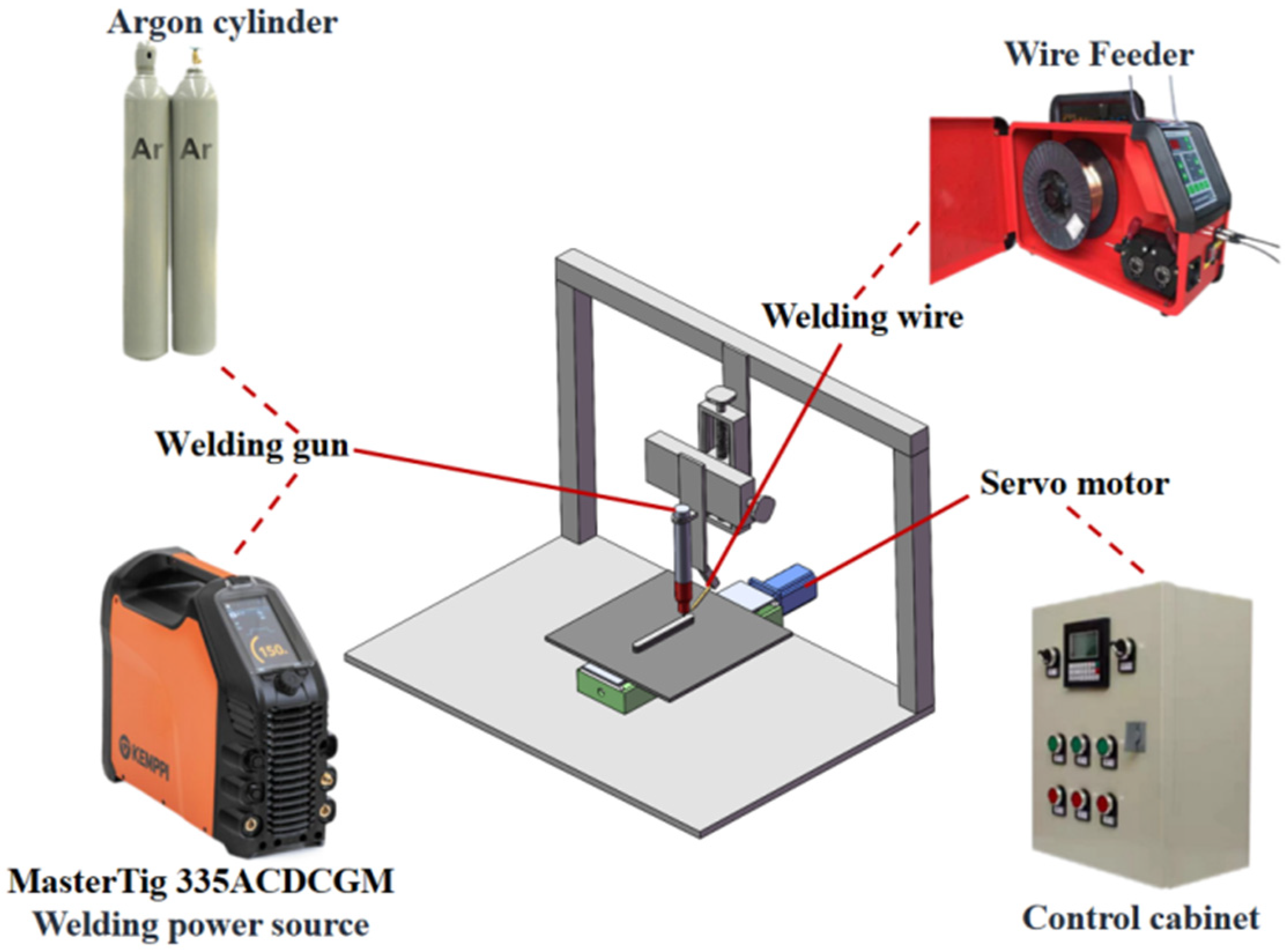
2. Experimental Materials and Methods
2.1. Test Material
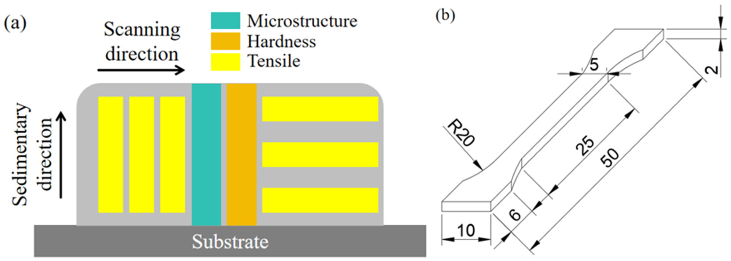
2.2. Test Methods
3. Results and Discussions
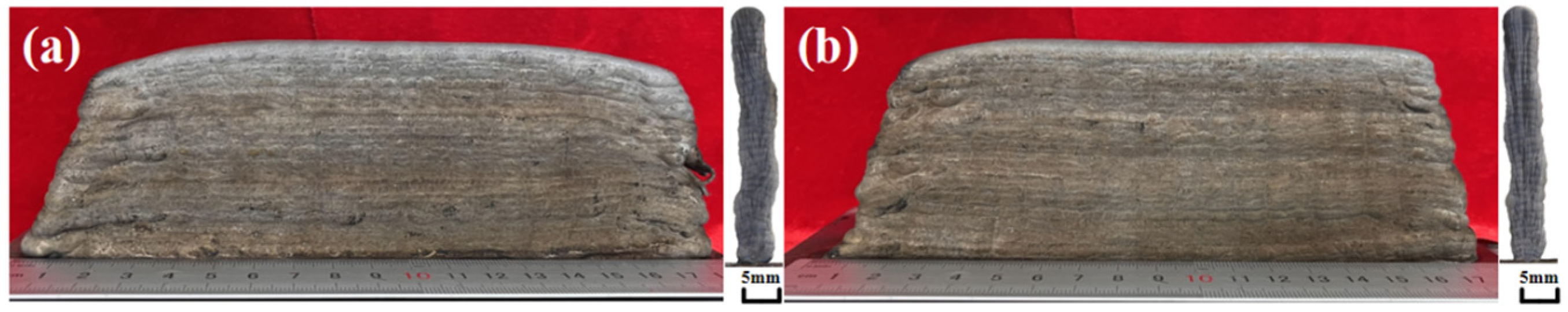
3.1. Macroscopic Appearance and Dimensions
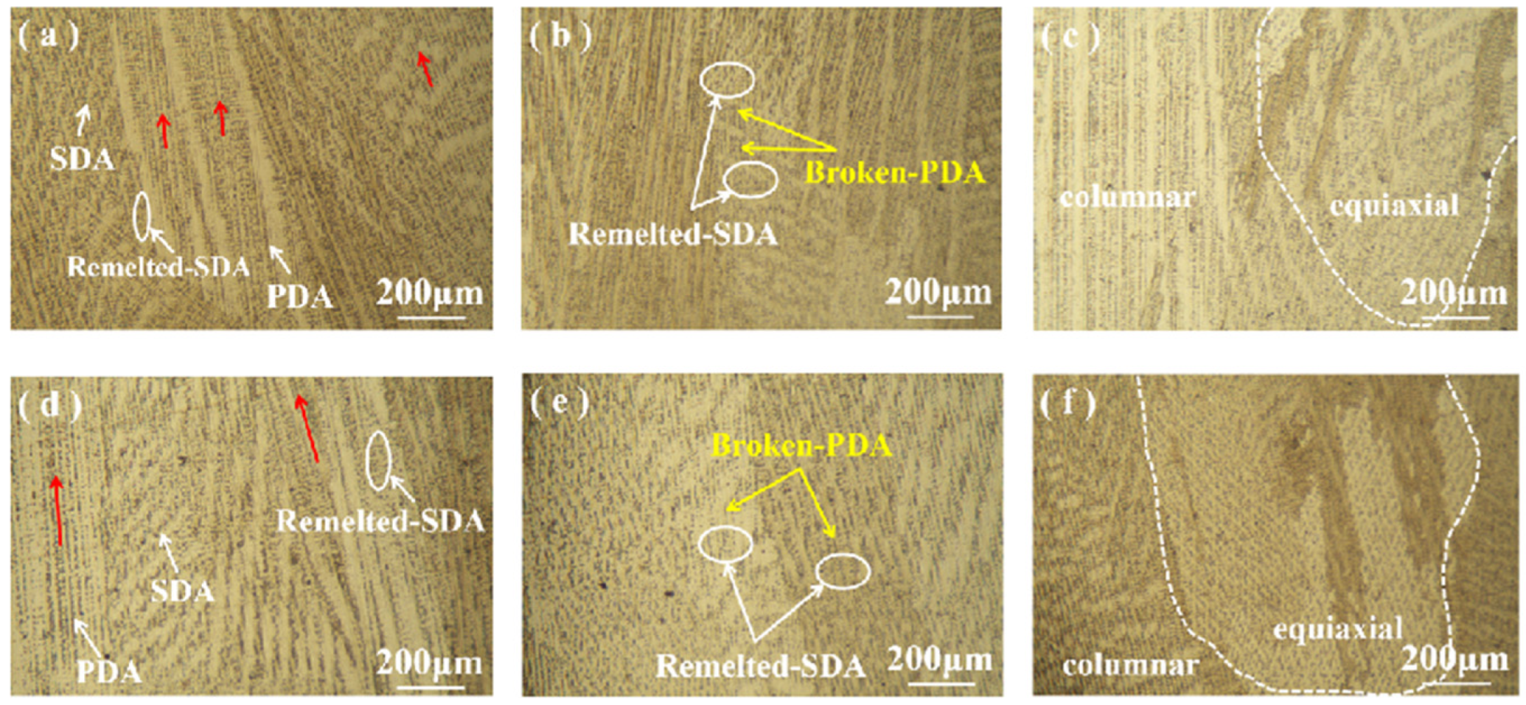
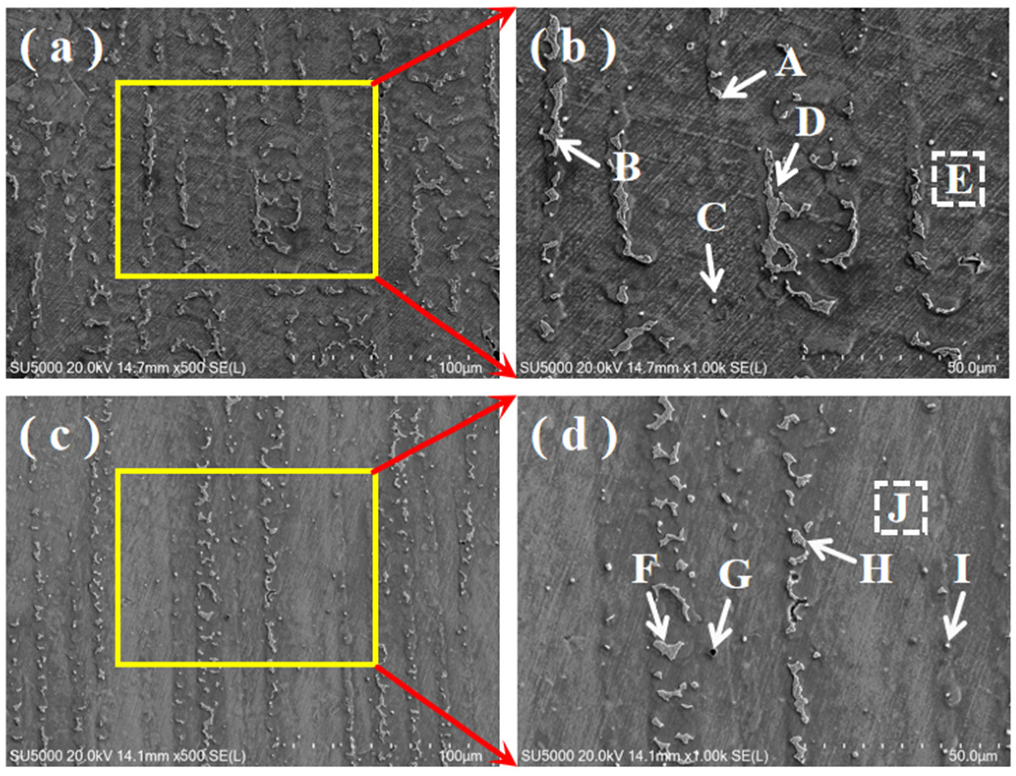
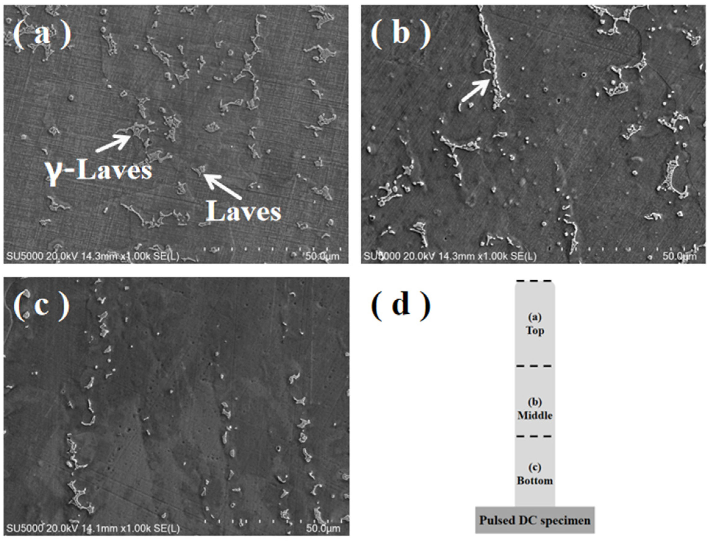
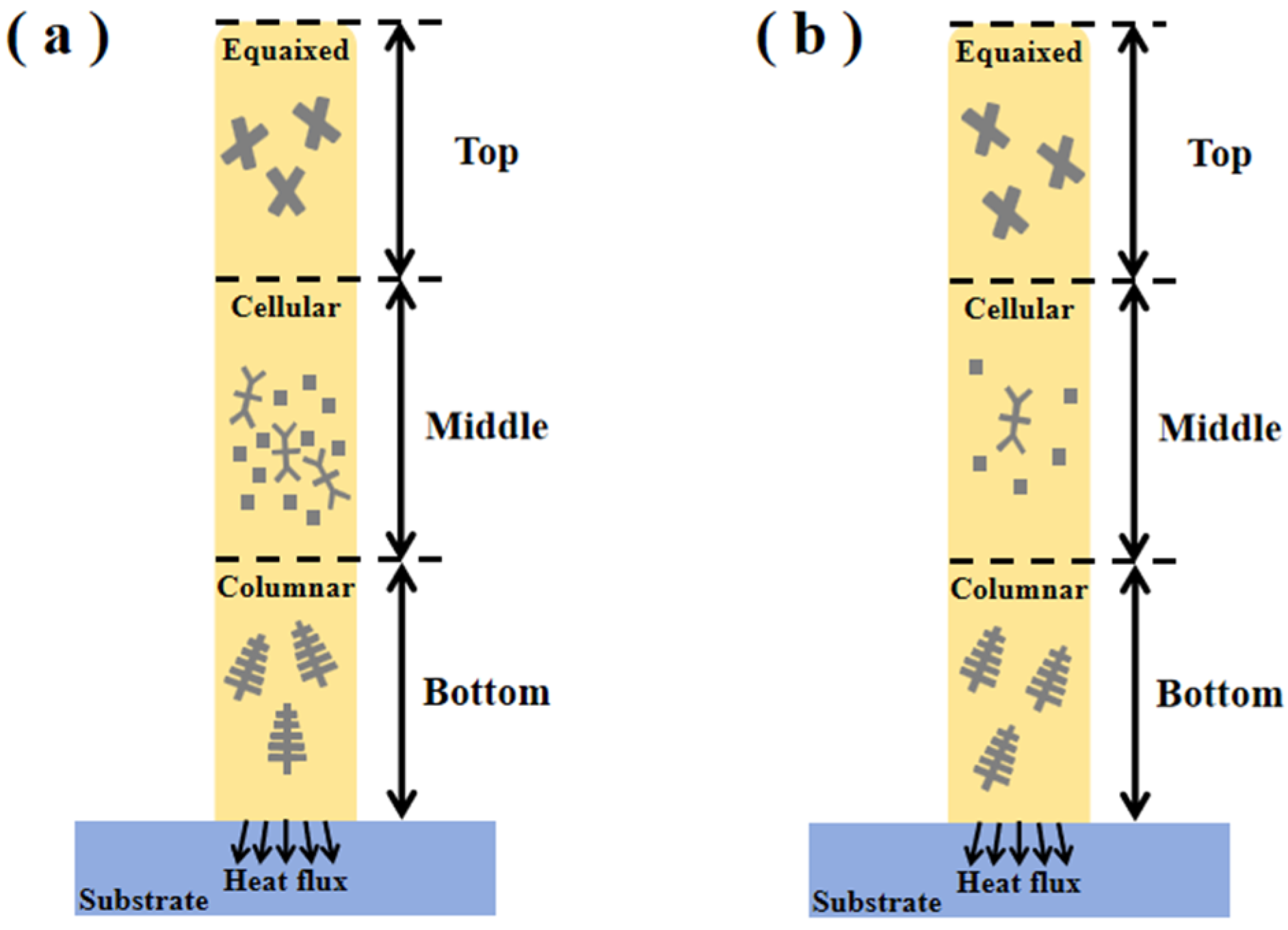
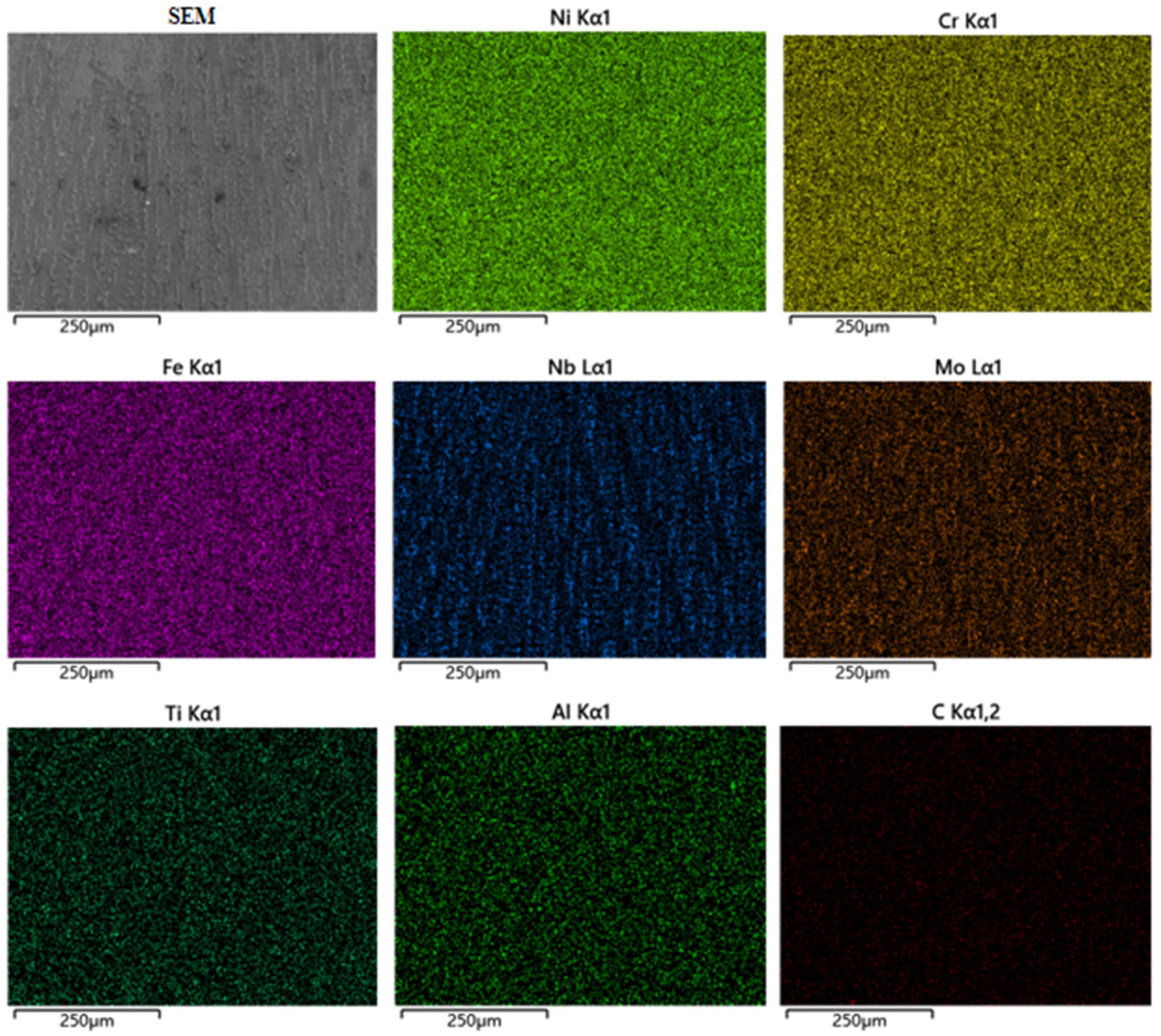
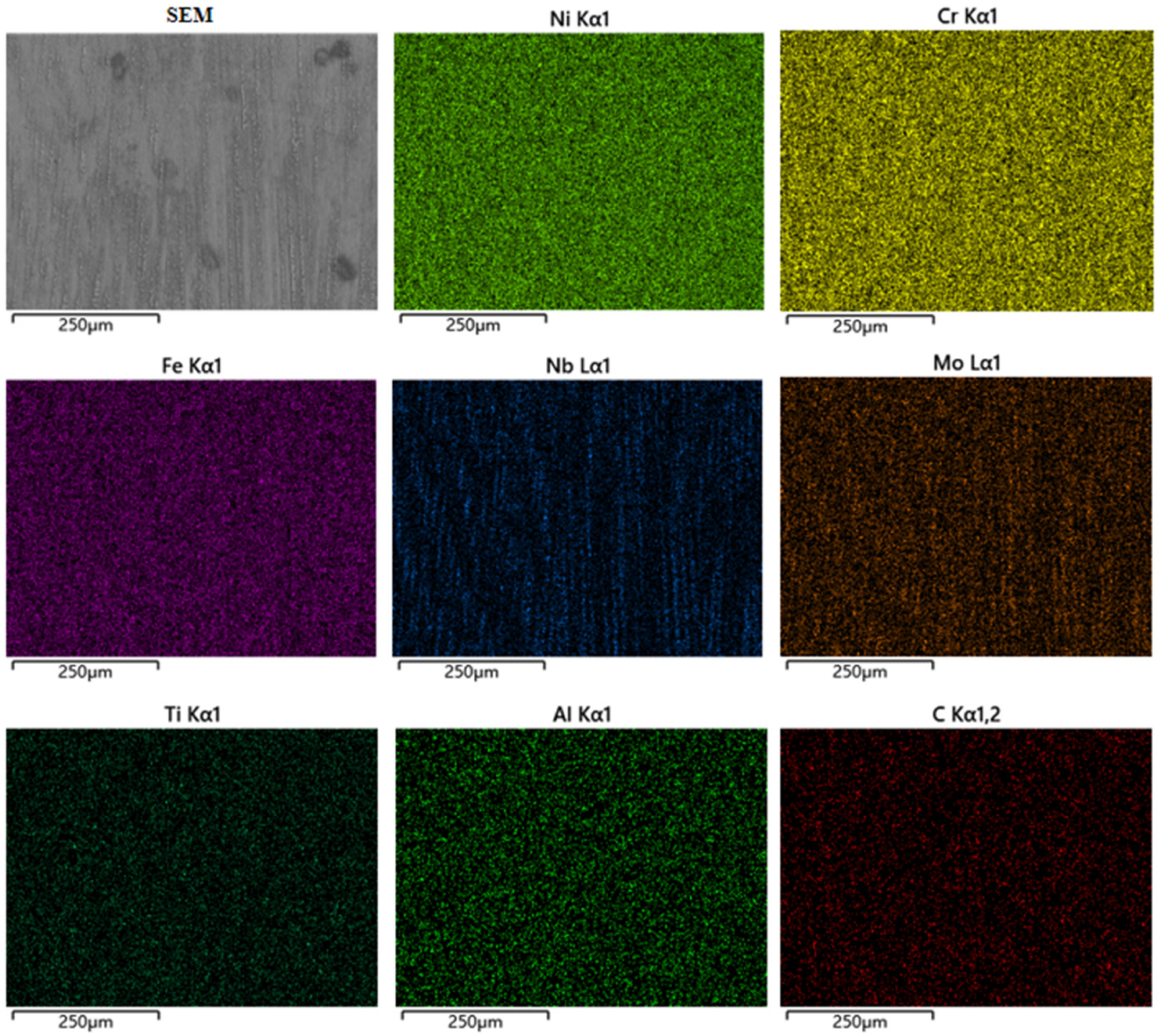
3.2. Microstructural Analysis
3.3. Mechanical Properties
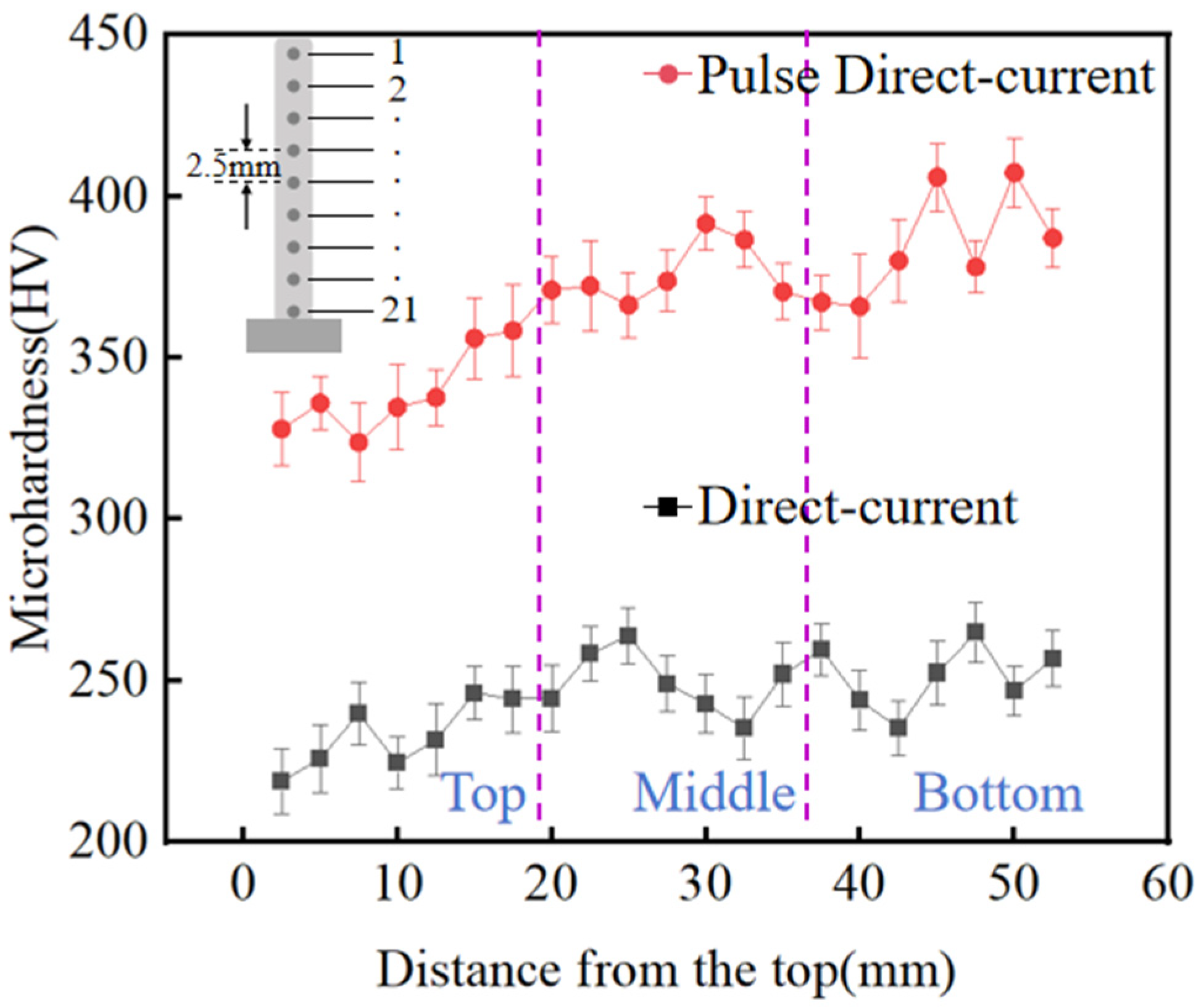
3.3.1. Microhardness
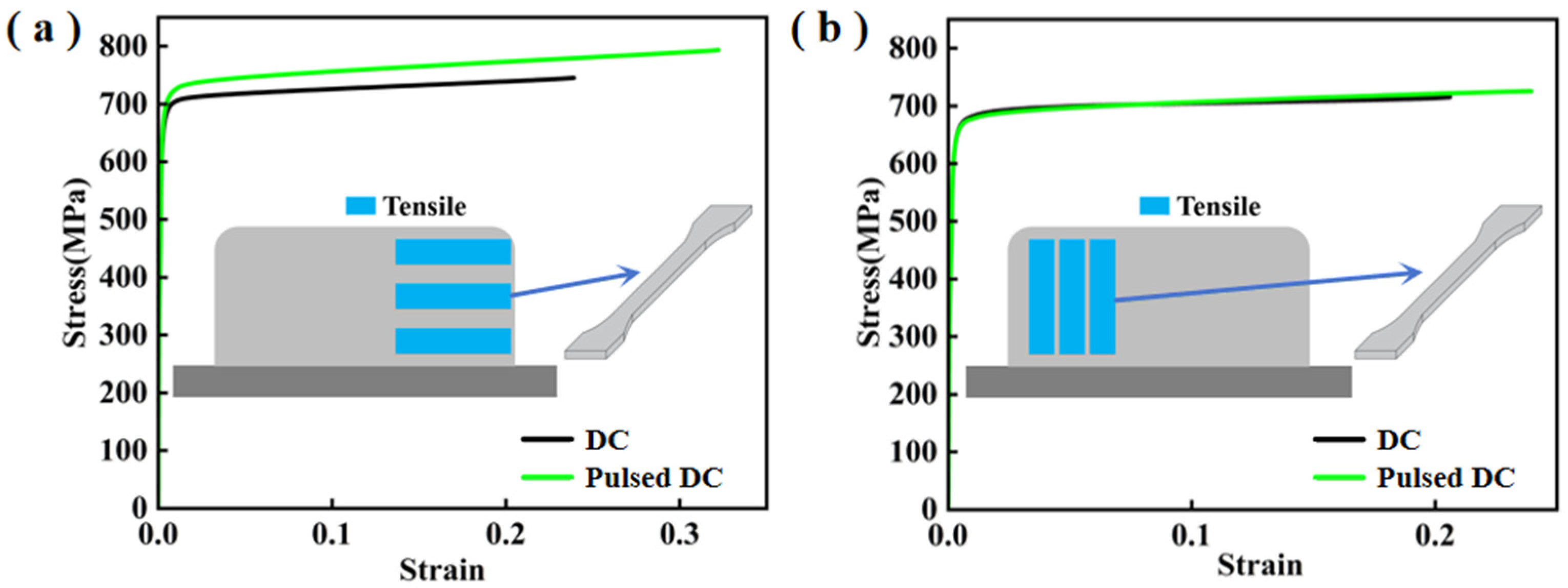
3.3.2. Tensile Properties
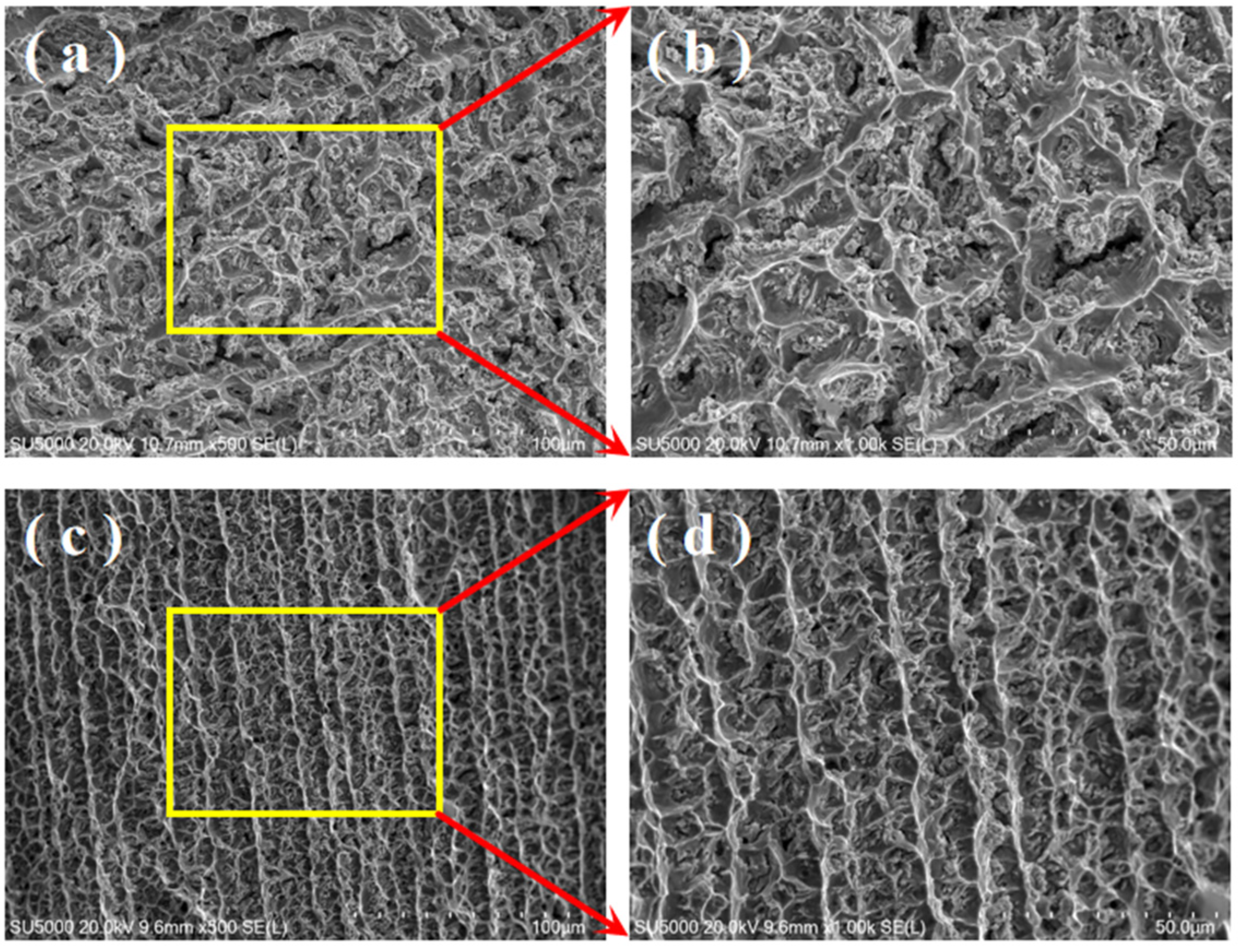
3.4. Fracture Morphology
4. Conclusions
- The overall forming process of the components was relatively stable under DC TIG additive manufacturing and pulsed DC TIG additive manufacturing processes. In the reciprocating deposition process, the average layer thicknesses were 1.57 mm and 1.43 mm, respectively, and the depth-to-width ratios of the weld channels of the pulsed DC deposition specimens were relatively low. The deposited layer became flatter after adding the pulse, which was conducive to maintaining the stability of the molten pool during the deposition process and improving the forming accuracy.
- The microstructure distribution of the sedimentary layer from bottom to top was relatively heterogeneous. The bottom layer was columnar dendrites, the middle layer was cellular crystals, and the top layer was equiaxed crystals. Compared with the DC TIG additive manufacturing of the GH4169 high-temperature alloy specimens, the Laves phase of the pulsed DC specimens was significantly reduced, which improved the plasticity and toughness of the material.
- The carbon content of the DC deposition specimen was higher than that of the pulsed DC deposition specimen. Higher carbide content in a certain region will lead to a decrease in tensile strength and microhardness in the corresponding region, which is very unfavourable to the properties of the GH4169 high-temperature alloy. The pulsed DC TIG additive manufacturing process for the GH4169 high-temperature alloy optimised this phenomenon.
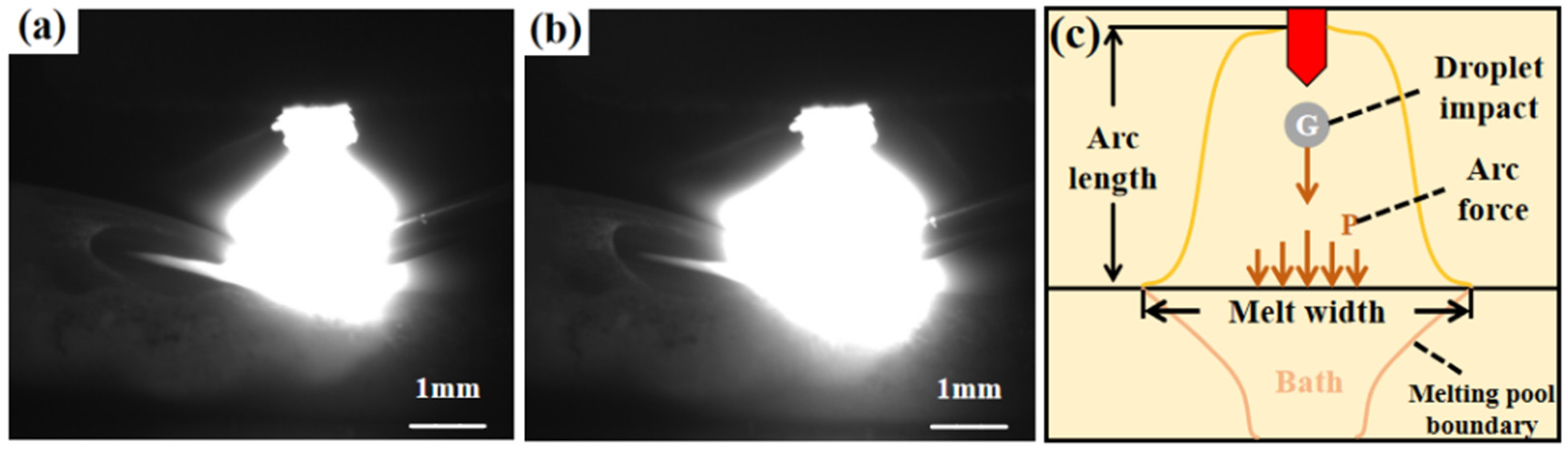
- The droplet transition modes of the DC and pulsed DC deposition samples were large droplet transition and fine droplet transition, respectively. The fine-drop transition mode under pulsed conditions had better directivity and less splashing, which was more conducive to ensuring the forming accuracy and process stability of the components.
- Both the DC-deposited specimens and the pulsed DC-deposited specimens showed significant anisotropy in the overall mechanical properties. The strengths in the horizontal direction were higher than those in the vertical direction by 30.07 MPa and 67.17 MPa, respectively. This apparent property inhomogeneity affected the performance of the components.
- The fracture morphology of the DC-deposited specimen showed a large surface of ligament foci and exhibited a crystal penetrating ductile damage mode. The fracture morphology of the pulsed DC-deposited specimen, where a large number of finer brittle nests could be observed, indicated a ductile damage mode.
Author Contributions
Funding
Institutional Review Board Statement
Informed Consent Statement
Data Availability Statement
Conflicts of Interest
References
- Pei, S.; Xue, F.; Zhou, Y.; Pan, C.; Jia, K. Effects of cryogenic gas jet cooling on milling surface roughness and tool life for GH4169 alloy additive manufacturing parts. J. Manuf. Process. 2023, 86, 266–281. [Google Scholar] [CrossRef]
- Chen, S.; He, Z.; Xiao, J.; Gai, S.; Wang, S.; Li, J. Modified heat treatment and related microstructu-re mechanical property evolution of arc melting additively manufactured GH4169 Ni-based superalloy. J. Alloys Compd. 2023, 947, 169449. [Google Scholar] [CrossRef]
- Yan, S.; Wang, Q.; Chen, X.; Zhang, C.; Cui, G. Fabrication of highly compact Inconel718 alloy by spark plasma sintering and solution treatment followed by aging. Vacuum 2019, 163, 194–203. [Google Scholar] [CrossRef]
- Deng, D.; Peng, R.L.; Brodin, H.; Moverare, J. Microstructure and mechanical properties of In-conel 718 produced by selective laser melting: Sample orientation dependence and effects of post heat treatments. Mater. Sci. Eng. A—Struct. Mater. Prop. Microstruct. Process. 2018, 713, 294–306. [Google Scholar] [CrossRef]
- Polonsky, A.T.; Echlin, M.P.; Lenthe, W.C.; Dehoff, R.R.; Kirka, M.M.; Pollock, T.M. Defects and 3D structural inhom-ogeneity in electron beam additively manufactured Inconel 718. Mater. Charact. 2018, 143, 171–181. [Google Scholar] [CrossRef]
- Ding, J.; Colegrove, P.; Mehnen, J.; Williams, S.; Wang, F.; Almeida, P.S. A computationally efficient finite element model of wire and arc additive manufacture. Int. J. Adv. Manuf. Technol. 2013, 70, 227–236. [Google Scholar] [CrossRef]
- Yu, S.F.; Yu, R.Z.; He, T.Y.; Dai, Y.L. Wire arc additive manufacturing and its application: Research progress. Materials 2021, 40, 198–209. [Google Scholar] [CrossRef]
- Clark, D.; Bache, M.R.; Whittaker, M.T. Microstructural characterization of a polycrystalline nickel based superalloy processed via tungsten inert gas shaped metal deposition. Metall. Mater. S Trans. B 2010, 41, 1346–1353. [Google Scholar] [CrossRef]
- Busachi, A.; Erkoyuncu, J.; Colegrove, P.; Martina, F.; Ding, J. Designing a WAAM Based Manufa-cturing System for Defence Applications. Procedia CIRP 2015, 37, 48–53. [Google Scholar] [CrossRef]
- Ding, J.; Colegrove, P.; Mehnen, J.; Ganguly, S.; Almeida, P.S.; Wang, F.; Williams, S. Thermo-mechanical analysis of wire and arc additive layer manufacturing process on large multi-layer parts. Comput. Mater. Sci. 2011, 50, 3315–3322. [Google Scholar] [CrossRef]
- Chen, W.; Chen, Y.H.; Mao, Y.Q. Research progress in additive manufacturing technology of aluminum alloy. J. Netshape Form. Eng. 2017, 9, 214–219. [Google Scholar] [CrossRef]
- Bai, J.Y.; Wang, J.H.; Lin, S.B.; Yang, C.L.; Fan, C.L. Model for multi-beads overlapping calculation in GTA-additive manufacturing. J. Mech. Eng. 2016, 52, 92–102. [Google Scholar] [CrossRef]
- Guo, J.; Zhou, Y.; Liu, C.; Wu, Q.; Chen, X.; Lu, J. Wire arc additive manufacturing of AZ31 magnesium alloy:grain refinement by adjusting pulse frequency. Materials 2016, 9, 823–836. [Google Scholar] [CrossRef]
- Wu, Q.; Ma, Z.; Chen, G.; Liu, C.; Ma, D.; Ma, S. Obtaining fine microstructure and unsupported overhangs by low heat input pulse arc additive manufacturing. J. Manuf. Ng Process. 2017, 27, 198–206. [Google Scholar] [CrossRef]
- Wang, H.; Jiang, W.; Ouyang, J.; Kovacevic, R. Rapid prototyping of 4043 Al-alloy parts by VP-GTAW. J. Mater. Process. Technol. 2004, 148, 93–102. [Google Scholar] [CrossRef]
- Zhang, X.H.; Ma, P.Z.; Zhang, K.; Chen, J.Q.; Chen, H. Study on controlling of welding seam microstructure about nickel-based high-temperature alloy by pulse TIG welding process. J. Mech. Eng. 2018, 54, 93–101. [Google Scholar] [CrossRef]
- Wang, F.; Williams, S.; Colegrove, P.; Antonysamy, A.A. Microstructure and mechanical properties of wire and arc additive manufactured Ti-6Al-4V. Metall. Mater. Trans. A 2012, 44, 968–977. [Google Scholar] [CrossRef]
- Wang, F.; Williams, S.; Rush, M. Morphology investigation on direct current pulsed gas tungsten arc welded additive layer manufactured Ti6Al4V alloy. Int. J. Adv. Manuf. Technol. 2011, 57, 597–603. [Google Scholar] [CrossRef]
- Guo, L.L.; Zheng, H.L.; Liu, S.H.; Feng, C.Y.; Li, Y.Q. Formation quality optimization and performance of INCONEL 625 cladding using hot-wire pulsed TIG. Rare Met. Mater. Eng. 2016, 45, 2219–2226. [Google Scholar]
- Ouyang, J.H.; Wang, H.; Kovacevic, R. Rapid prototyping of 5356-aluminum alloy based on variable polarity gas tungsten arc welding: Process control and microstructure. Mater. Manuf. Process. 2002, 17, 103–124. [Google Scholar] [CrossRef]
- Katou, M.; Oh, J.; Miyamoto, Y.; Matsuura, K.; Kudoh, M. Freeform fabrication of titanium metal and intermetallic alloys by three-dimensional micro welding. Mater. Des. 2006, 28, 2093–2098. [Google Scholar] [CrossRef]
- GB/T 700-2006; Carbon Structural Steels-Part 5: Grades and Chemical Composition. National Standardization Administration: Beijing, China, 2016.
- GB/T 228.1-2021; Metallic Materials-Tensile Testing-Part 1: Method of Test at Room Temperature. National Standardization Administration: Beijing, China, 2021.
- GB/T 4340.4-2022; Metallic Materials—Vickers Hardness Test—Part 4: Tables of Hardness Values. National Standardization Administration: Beijing, China, 2022.
- Liu, Z.; Zhao, D.; Wang, P.; Yan, M.; Yang, C.; Chen, Z.; Lu, J.; Lu, Z. Additive manufacturing of metals: Microstructure evolution and multistage control. J. Mater. Sci. Technol. 2022, 100, 224–236. [Google Scholar] [CrossRef]
- Cakmak, E.; Kirka, M.M.; Watkins, T.R.; Cooper, R.C.; An, K.; Choo, H.; Wu, W.; Dehoff, R.R.; Babu, S.S. Microstructural and micromechanical characterization of IN718 theta shaped specimens built with electron beam melting. Acta Mater. 2016, 108, 161–175. [Google Scholar] [CrossRef]
- Tucho, W.M.; Cuvillier, P.; Sjolyst-Kverneland, A.; Hansen, V. Microstructure and hardness studies of Inconel 718 manufactured by selective laser melting before and after solution heat treatment. Mater. Sci. Eng. A 2017, 689, 220–232. [Google Scholar] [CrossRef]
- Li, J.; Zhao, Z.; Bai, P.; Qu, H.; Liu, B.; Li, L.; Wu, L.; Guan, R.; Liu, H.; Guo, Z. Microstructural evolution and mechanical properties of IN718 alloy fabricated by selective laser melting following different heat treatments. J. Alloys Compd. 2019, 772, 861–870. [Google Scholar] [CrossRef]
- Sui, S.; Tan, H.; Chen, J.; Zhong, C.; Li, Z.; Fan, W.; Gasser, A.; Huang, W. The influence of Laves phases on the room temperature tensile properties of Inconel 718 fabricated by powder feeding laser additive manufacturing. Acta Mater. 2019, 164, 413–427. [Google Scholar] [CrossRef]
- Manikandan, S.; Sivakumar, D.; Kamaraj, M.; Rao, K.P. Laves Phase Control in Inconel 718 Weldments. Mater. Sci. Forum. 2012, 1563, 614–619. [Google Scholar] [CrossRef]
- Shi, Z.X.; Xu, G.H.; Liu, N.; Tian, W.; Chen, J.C.; Tang, C.J.; Zhu, Y.; Zhang, L.J. Effect of C content on microstructure and mechanical properties of GH4169 alloy. Rare Met. Mater. Eng. 2023, 52, 2926–2934. [Google Scholar] [CrossRef]
- Jia, C.S.; Xiao, K.M.; Yin, X.Q. Plasma flow force of welding arc. Trans. China Weld. Inst. 1994, 2, 101–106. Available online: http://hjxb.hwi.com.cn/hjxb/article/id/19940206 (accessed on 19 July 2024).


| C | Mn | Si | S | P | Fe |
|---|---|---|---|---|---|
| 0.14–0.22 | 0.30–0.65 | ≤0.30 | ≤0.050 | ≤0.045 | Balance |
| C | Cr | Mo | Ni | Nb | Ti | Al | Si | Mn | P | S |
|---|---|---|---|---|---|---|---|---|---|---|
| 0.037 | 19.5 | 3.11 | 52.9 | 5.16 | 0.88 | 0.38 | 0.10 | 0.10 | 0.005 | 0.003 |
| Specimen | Wire Feed Speed Vf/(cm/min) | Welding Speed Vh/(mm/min) | Average Current I/A | Peak Current I/A | Base Value Current I/A | Duty Cycle (%) | Pulse Frequency (HZ) |
|---|---|---|---|---|---|---|---|
| A (DC) | 350 | 300 | 250 | - | - | - | - |
| B (Pulsed DC) | 350 | 300 | 250 | 294 | 206 | 50 | 300 |
| Element (wt.%) | C | Al | Ti | Cr | Fe | Ni | Nb | Mo |
|---|---|---|---|---|---|---|---|---|
| Spectrum A | 0.00 | 0.16 | 0.82 | 19.46 | 19.46 | 47.47 | 10.25 | 4.87 |
| Spectrum B | 0.00 | 0.21 | 1.50 | 10.53 | 19.35 | 46.38 | 18.08 | 3.95 |
| Spectrum C | 12.74 | 0.45 | 1.43 | 18.18 | 14.03 | 45.31 | 5.22 | 2.63 |
| Spectrum D | 0.00 | 0.33 | 1.57 | 11.68 | 16.78 | 43.69 | 22.5 | 3.45 |
| Spectrum E | 1.09 | 0.49 | 0.66 | 19.05 | 17.44 | 55.37 | 3.05 | 2.84 |
| Element (wt.%) | C | Al | Ti | Cr | Fe | Ni | Nb | Mo |
|---|---|---|---|---|---|---|---|---|
| Spectrum F | 0.00 | 0.57 | 1.04 | 18.63 | 18.08 | 47.05 | 11.15 | 3.48 |
| Spectrum G | 16.51 | 0.81 | 1.96 | 12.31 | 12.76 | 45.07 | 5.50 | 5.07 |
| Spectrum H | 0.00 | 1.13 | 1.13 | 16.11 | 13.77 | 48.78 | 15.54 | 3.54 |
| Spectrum I | 0.00 | 0.25 | 1.34 | 13.14 | 10.94 | 49.05 | 20.55 | 4.74 |
| Spectrum J | 0.89 | 0.54 | 0.60 | 19.12 | 17.86 | 55.72 | 2.51 | 2.77 |
| Element (wt.%) | C | Al | Ti | Cr | Fe | Ni | Nb | Mo |
|---|---|---|---|---|---|---|---|---|
| A (DC) | 9.82 | 0.45 | 0.85 | 18.19 | 16.35 | 46.39 | 4.9 | 3.04 |
| B (Pulsed DC) | 7.91 | 0.46 | 0.85 | 18.69 | 16.73 | 47.24 | 4.99 | 3.14 |
| Specimen | Horizontal Direction | Horizontal Direction | Vertical Direction | Vertical Direction |
|---|---|---|---|---|
| Tensile Strength | Elongation | Tensile Strength | Elongation | |
| (MPa) | (%) | (MPa) | (%) | |
| A (DC) | 745 | 23.89 | 714.93 | 20.66 |
| B (Pulsed DC) | 792.47 | 32.21 | 725.3 | 23.94 |
Disclaimer/Publisher’s Note: The statements, opinions and data contained in all publications are solely those of the individual author(s) and contributor(s) and not of MDPI and/or the editor(s). MDPI and/or the editor(s) disclaim responsibility for any injury to people or property resulting from any ideas, methods, instructions or products referred to in the content. |
© 2024 by the authors. Licensee MDPI, Basel, Switzerland. This article is an open access article distributed under the terms and conditions of the Creative Commons Attribution (CC BY) license (https://creativecommons.org/licenses/by/4.0/).
Share and Cite
Zhang, X.; Zhang, J.; Xie, X.; Jiang, Z.; Chen, C.; Wu, Z.; Zhang, Y. Effect of Current Waveform on Microstructure Evolution and Mechanical Properties of GH4169 High-Temperature Alloy Tungsten Inert Gas Additive Manufacturing. Materials 2024, 17, 4649. https://doi.org/10.3390/ma17184649
Zhang X, Zhang J, Xie X, Jiang Z, Chen C, Wu Z, Zhang Y. Effect of Current Waveform on Microstructure Evolution and Mechanical Properties of GH4169 High-Temperature Alloy Tungsten Inert Gas Additive Manufacturing. Materials. 2024; 17(18):4649. https://doi.org/10.3390/ma17184649
Chicago/Turabian StyleZhang, Xinlong, Jiaao Zhang, Xiaodong Xie, Zhaosong Jiang, Chao Chen, Zhe Wu, and Yang Zhang. 2024. "Effect of Current Waveform on Microstructure Evolution and Mechanical Properties of GH4169 High-Temperature Alloy Tungsten Inert Gas Additive Manufacturing" Materials 17, no. 18: 4649. https://doi.org/10.3390/ma17184649