Article

Effect of Deposition Temperature on Zn Interstitials and Oxygen Vacancies in RF-Sputtered ZnO Thin Films and Thin Film-Transistors

by
Sasikala Muthusamy
,
Sudhakar Bharatan
*,
Sinthamani Sivaprakasam
and
Ranjithkumar Mohanam
Department of Electrical and Electronics Engineering, Sri Venkateswara College of Engineering, Sriperumbudur 602117, India
*
Author to whom correspondence should be addressed.
Materials 2024, 17(21), 5153; https://doi.org/10.3390/ma17215153
Submission received: 20 September 2024 / Revised: 12 October 2024 / Accepted: 16 October 2024 / Published: 23 October 2024

Abstract

:
ZnO thin films were deposited using RF sputtering by varying the argon:oxygen gas flow rates and substrate temperatures. Structural, optical and electrical characterization of ZnO thin films were systematically carried out using X-Ray diffraction (XRD), scanning electron microscopy (SEM), UV–visible spectroscopy, X-Ray photoelectron spectroscopy (XPS) and Hall measurements. Film deposited at room temperature and annealed at 300 °C exhibited low O2 incorporation with localized defects and a high percentage of Zn interstitials. A large crystalline size and fewer grain boundaries resulted in a high Hall mobility of 46.09 cm2/V-s Deposition at higher substrate temperatures resulted in improvement in O2 incorporation through the annihilation of localized defects and decrease in oxygen vacancies and Zn interstitials. Urbach tails within the bandgap were identified using the absorption spectrum and compared with the % defects from XPS. Bottom-gate thin-film transistors were subsequently fabricated on a SiO2/p-Si substrate using the combination of RF sputtering, wet etching and photolithography. Variation in the substrate temperature showed performance enhancement in terms of the leakage current, threshold voltage, sub-threshold swing and ION/IOFF ratio. Thin-film transistor (TFT) devices deposited at 300 °C resulted in an O2-rich surface through chemisorption, which led to a reduction in the leakage current of up to 10−12 A and a 10-fold reduction in the sub-threshold swing (SS) from 30 V to 2.8 V. Further TFT optimization was carried out by reducing the ZnO thickness to 50 nm, which resulted in a field-effect mobility of 1.1 cm2/V-s and ION/IOFF ratio of 105.

1. Introduction

Enormous research efforts on metal oxide semiconductors have been carried out in the recent past, due to which, they have become promising candidates in the field of solar cells [1,2,3,4], thin-film transistors (TFTs) [5,6,7,8], photodetectors [9,10,11,12], memory [13,14,15], gas sensors [16,17,18,19], bio sensors [20,21,22] and complementary metal oxide semiconductor (CMOS) circuits [23,24]. Ease of availability of metal oxide proves to be a key attribute in realizing terrestrial thin-film solar cells, detectors and TFTs. Even though the efficiencies of metal oxide (ZnO and TiO2) thin-film solar cells are lower compared to perovskite solar cells (26.7% efficiency) [25], metal oxides play a vital role in improving the efficiency and chemical stability of solar cells. Electrical and optical properties such as a wide bandgap (3.37 eV direct bandgap in the case of ZnO) [26], high mobility, transparency, tunability and substrate compatibility make metal oxides a promising candidate in photodetector and gas sensing applications such as UV sensing, optoelectronics, imaging (medical imaging) and environmental monitoring [9,10,11,12].
In many of the traditional electronic applications, e.g., pixel and peripheral driver circuits, amorphous silicon (Si)-based TFTs are widely used due to their ease of integration with a complementary metal oxide semiconductor (CMOS). However, large transistor sizing limits the application of TFTs in integrated circuits [27]. Further, advancements in the fields of the Internet of Things (IOT), artificial intelligence (AI) and machine learning (ML) require large memory and high bandwidth, leading to the scaling down and 3D integration of devices. There have been reports on stacked In2O3 TFTs on a SiO2/Si substrate in a 3D integration form of devices [28]. Even though Si technology can easily be realized with advanced manufacturing processes, its performance suffers due to a high process temperature, poor mobility, bias stress, threshold voltage instability and reliability issues. Hence, metal oxide-based TFTs are the potential alternative to Si-based TFTs in the areas of flexible display, health care, environment and automotive applications. The process-level advantage of an oxide semiconductor is the ability to realize large-area device performance on any substrate at low process temperatures using a non-equilibrium deposition technique such as RF sputtering.
Among the various metal oxide semiconductor cations, Zn and Sn are considered to be non-toxic and abundantly available. ZnO exhibits a wide bandgap (3.37 eV) [26], low cost and excellent electrical and optical properties, which makes it a promising candidate for numerous electronic applications. Traditionally, ZnO thin films are deposited using a variety of processes, such as spin coating [29], spray analysis [30,31], pulsed laser deposition [32], molecular-beam epitaxy [33,34], atomic layer deposition [35,36] and RF sputtering [37,38,39]. A highest mobility of 300 cm2/V-s has been achieved [34] in Mg-doped ZnO heterostructures grown using molecular-beam epitaxy. This requires an ultra-high vacuum, leading to high cost. Alternatively, RF sputtering provides versatility, scalability, uniformity and high-quality thin films in a controlled environment even at low temperatures. This has paved the way for large-area and low-cost device applications.
Even though the mobilities of RF-sputtered ZnO thin films have reached the range of 70 cm2/V-s, defects in the ZnO thin films play a crucial role in realizing high-quality TFTs [40,41]. Various intrinsic defects such as oxygen vacancies, Zn interstitials, grain boundaries and dislocations are reported to play a major role in forming n-type semiconductors [42,43]. Among these, oxygen vacancies and Zn interstitials can act as shallow donors and/or deep acceptors depending on the charge state that would affect the optical and electrical properties. Advanced characterization techniques like X-Ray photoelectron spectroscopy (XPS), X-Ray diffraction (XRD) and UV–visible spectroscopy were employed to understand and manipulate the defects in thin-film optimization.
Singh S et al. reported a field-effect mobility of 0.6134 cm2/V-s and threshold voltage of 3.1 V in their ZnO TFT using RF sputtering with SiO2 as a gate insulator [38]. Similarly, Jong Hoon Lee et al. fabricated ZnO TFT with MgO as a gate insulator and reported a lower field-effect mobility of 0.0235 cm2/V-s, ION/IOFF ratio of ∼105, threshold voltage of 2.2 V and sub-threshold (SS) value of 1.18 V/decade [39]. Brandon Walker et al. compared the performance of a ZnO TFT with various gate dielectric materials, namely, Al2O3, HfO2 and ZrO2, and achieved the highest on/off ratio of >105 [44]. B. -S. Wang et al. achieved a mobility of 84.22 cm2/V-s and an ION/IOFF ratio of 3 × 10⁶ on a MgZnO/ZnO heterostructure TFT. It may be noted that the presence of defects such as O2 vacancies and Zn interstitials in ZnO significantly affects various electrical parameters, which are crucial for the realization of a normally off device (enhancement-type transistor) [45].
In this work, RF sputtering has been preferred over other techniques because of its non-equilibrium, large-area growth capability, and its ease of processing at low temperatures. Various properties of ZnO thin films were characterized by X-Ray diffraction, XPS, Hall measurements, SEM imaging and a UV–visible spectrophotometer. Hence, in this paper, the optimization of ZnO thin films has been systematically carried out using an RF sputtering technique with different argon:oxygen flow rates and different substrate temperatures. Based on the thin-film optimization, bottom-gate TFTs were fabricated and various device parameters such as the threshold voltage, ION/IOFF ratio, field-effect mobility and sub-threshold swing were investigated.

2. Materials and Methods

2.1. Deposition of ZnO Thin Films

ZnO thin films were deposited using RF magnetron sputtering on p-Si substrate with a resistivity of 5–10 Ω-cm. Prior to ZnO deposition, substrates were cleaned using RCA1 and RCA2 methods to remove organic and metal contaminations, followed by HF dip to remove native oxide [46]. During ZnO deposition, the target to substrate distance was maintained at 7.5 cm and the chamber was evacuated to 5.5 × 10⁻⁶ mbar. In order to maintain a contamination-free source material, the target was pre-sputtered for 10 min prior to the deposition. Further, a series of films were deposited at room temperature to optimize the Ar:O2 gas flow rate. Samples A, B and C represent 180 nm thick ZnO films deposited at different Ar:O2 flow rates, at a constant annealing temperature of 300 °C for 30 min in N2 ambient, as described in Table 1.
The gas flow rates were measured using the Aalborg mass flow controllers. Upon completion of the flow rate optimization, temperature optimization was carried out at room temperature (RT), 250 °C and 300 °C, as detailed in Table 1. Deposition rates of Samples D, C and E were determined to be 3 nm/min, 6 nm/min and 7 nm/min, respectively, using a Bruker profilometer (Bruker Nano Inc., Tucson, AZ, USA) (Figure S1).
Grazing incidence (GI) θ/2θ X-Ray diffraction was carried out on Samples A, B, C, D and E using a Rigaku Smartlab X-Ray Diffractometer (Rigaku corporation, Tokyo, Japan). Based on the FWHM values of the (002) XRD peak, various parameters such as the crystallite size, strain and dislocation density values were determined. Hall measurements were also carried out on the above samples at a magnetic field of 0.51 T using an Ecopia Van der Pauw HMS 3000 system (Ecopia, Anyang, Republic of Korea). Surface morphology of ZnO thin films was studied using a Zeiss ULTRA 55 scanning electron microscopy (Zeiss, OberKochen, Germany) (SEM) system on all the above samples. X-Ray photoelectron spectroscopy (XPS) analysis of the ZnO thin films was performed using a Kratos Axis Ultra spectrometer (Kratos Analytical, Manchester, UK), employing a monochromatic Al-Kα source. Absorption edges of all the above samples were derived from the transmission data measured in a UV-1650PC Shimadzu spectrophotometer (Shimadzu Corporation, Kyoto, Japan).

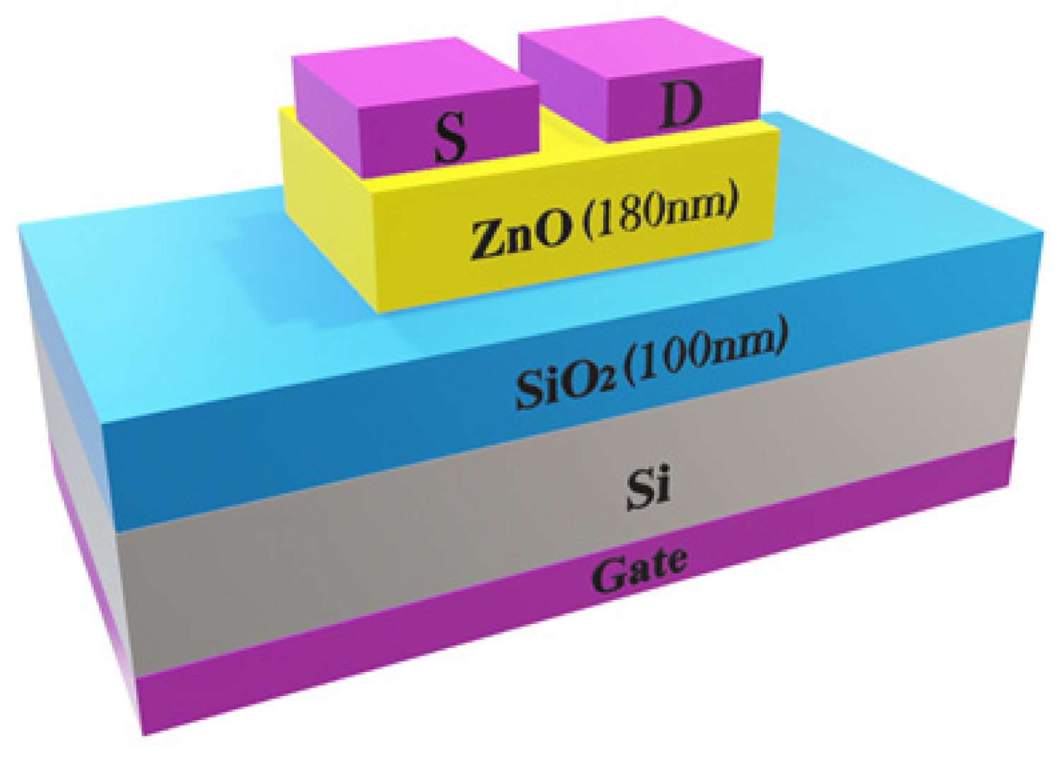
2.2. Device Fabrication and Characterization

Thin-film transistor devices with an optimized flow rate of 16:4 (Ar:O2) and 60 W RF power were fabricated on a single-side polished p-SiO2/Si (525 μm) substrate with an oxide thickness of 100 nm, procured from Prolyx Microelectronics Pvt., Ltd., Bengaluru, India. TFTs thus fabricated are named C1, D1 and E1 based on the variations in the process parameters, as listed in Table 2.
The mask for patterning the channel and electrode layer was printed on chrome glass using the mask writer (Figure S2). Exposure and patterning of the device were carried out on a Karl Suss MA6-BA6 mask aligner (SUSS Micro Tec., Garching, Germany). Figure 1 shows the schematic of the TFT device fabricated using a 2-step lithography process.
Firstly, 180 nm thick ZnO was deposited using RF sputtering, followed by the first lithography process wherein a 300 µm × 300 µm ZnO mesa structure was created by a wet etching process. Next, the second lithography was carried out to pattern the source and drain the electrodes. An amount of 100 nm Al metal was then deposited at room temperature using the thermal evaporation method, followed by a lift-off process, to obtain the desired source/drain (S/D) pattern. Finally, back-side SiO2 was selectively removed using HF dip, and blanket Al metal (100 nm) as the gate electrode was deposited using thermal evaporation. In order to improve the contact resistance, all the devices were annealed at 220 °C in N2 ambient for 10 min. Electrical properties of ZnO TFTs with a width to length (W/L) ratio of 50 µm/50 µm were examined using I–V transfer and output characteristics. I–V characteristics were carried out on a cascade Summit 11000B-M (Cascade Microtech, Beaverton, OR, USA) precision 4-axis semi-automated Probe station platform.

3. Results and Discussion

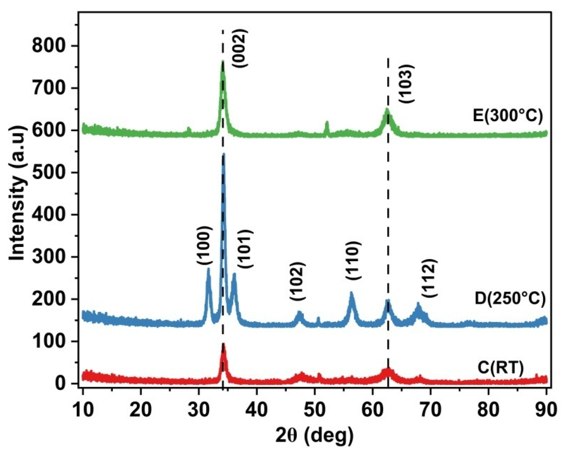
3.1. X-Ray Diffraction (XRD)
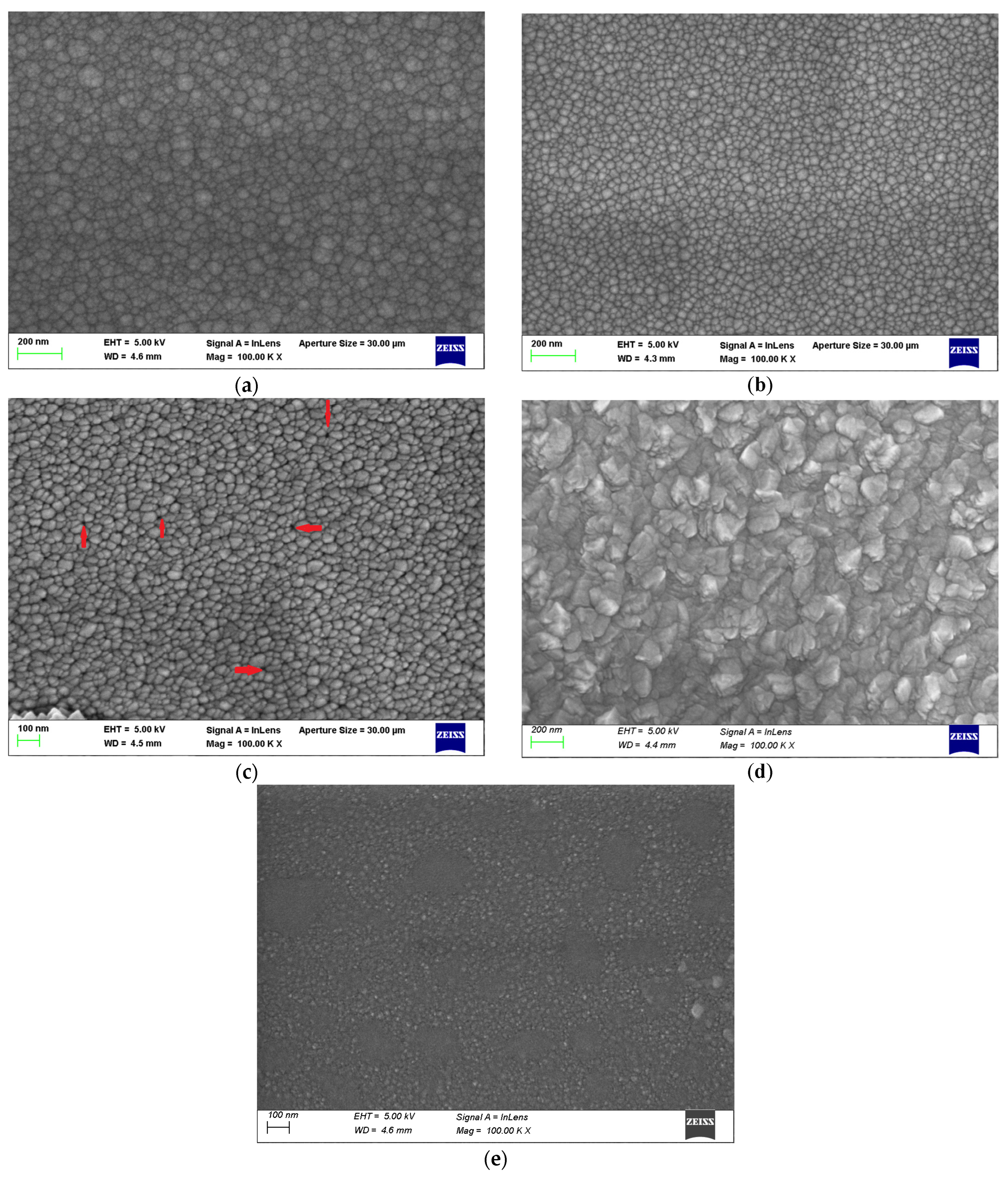
Figure 2 represents the grazing incident X-Ray diffraction of Samples A, B and C deposited at varying Ar:O2 flow rates. The XRD spectrum peaks match well with the data of JCPDS card no: 36-1451 [44]. Sample A showed a high-intensity (002) XRD peak at 34.53° and an even higher (103) peak at 62°. As the O2 ratio is increased in Samples B and C, the overall intensity of the ZnO (002) peak has decreased with the suppression of the (103) ZnO peak. The crystallite size, dislocation density and micro-strain were calculated using Equations (1)–(3) [47] and are listed in Table 3.
D = 0.9 λ β C o s θ
δ = 1 D 2
ε = β 4 tan θ
where λ is the wavelength of the X-Ray (1.54 Å), θ is the Bragg’s angle, β is the full width of half maximum (FWHM) of the XRD peak, δ is the dislocation density and D is the crystallite size.
Figure 3 compares the GIXRD of Samples C, D and E deposited at RT, 250 °C and 300 °C, respectively. By maintaining the Ar:O2 flow rate at 16:4, Samples D and E exhibited notable improvement in the (002) XRD peak as compared to Sample C, indicative of improvement in the crystalline quality. All the samples except Sample A exhibited preferred orientation along the (002) plane. Hence, all our TFT devices were grown at the optimized gas flow ratio of 16:4 (Ar:O2) at room temperature, 250 °C and 300 °C. It may be noted that Sample D exhibits a polycrystalline property with distinct peaks at (100), (002), (101), (102), (110), (103) and (112).
Table 3 lists the crystalline size calculated from the FWHM values of the XRD spectrum. Sample A exhibited the lowest (002) XRD FWHM and highest crystalline size, whereas Sample C demonstrated the highest FWHM and lowest crystalline size. Even though Sample A exhibited the lowest strain in the microstructure, the presence of a dominant (103) XRD peak suggests that the surface is affected by the non-equilibrium growth condition of RF sputtering. At higher deposition temperatures of 250 °C and 300 °C in Samples D and E, the crystallite size increased to 13.85 nm and 11.38 nm, respectively. The reason for the increase in the crystallite size in Sample D could be explained by the fact that higher substrate temperatures assist in the surface migration of atoms/ions, leading to the appearance of an in-plane (100) XRD peak at 31° (Figure 3).
Figure S3 shows the conventional X-Ray diffraction spectra of Sample C, which exhibits a dominant (002) ZnO peak at 34°, and a relatively low-intensity (103) peak at 62°, indicative of preferential (002) crystal formation in the bulk layer. The intensity ratio of the (002)/(103) peak has been observed to increase from 3 in GIXRD to 9.52 in conventional XRD, indicative of c-axis orientation in the bulk layer. The sharp (002) peak in conventional XRD is evidence of c-axis orientation, and the relatively higher (103) peak in GIXRD is evidence of surface re-structuring during the final stages of RF sputtering. Yunlan Wang et al. [48] reported in their RF-sputtered ZnO thin films that the appearance of (103) GIXRD orientation is due to the native property of ZnO. With RF sputtering being a non-equilibrium growth technique, the re-orientation of atoms by diffusion may happen on the surface during the final stages of deposition, which could be the reason for the presence of the dominant (103) peak. Additionally, (103) XRD peaks are reported in ZnO thin films prepared by electro-deposition [49] and sol–gel [50] processes. It is observed that Sample A has the highest (103) peak intensity compared to any other sample. This could be attributed to the relatively low oxygen reactive species, enabling the Zn atoms to move freely along the surface. As the O2 flow rates are increased in Samples B, C, D and E, the influx of O2 species suppressed the free movement or diffusion of Zn atoms, leading to a low-intensity (103) peak. Hence, O2 over-pressure during the sputtering process becomes vital in depositing a smooth surface.

3.2. SEM

Figure 4a–e show the SEM images of ZnO films A, B, C, D and E, respectively. Sample A, deposited at an Ar:O2 flow rate ratio of 20:0, shows a larger crystallite size with distinct contours. The presence of bigger grain crystalloids in the SEM image for Sample A corroborates the GIXRD data, revealing a crystallite size of 14.596 nm (Table 3). The crystallite size started to decrease with the highly dense surface morphology in Sample B. Both Samples A and B exhibit a granular and void-free surface with a high packing density. With a further increase in the O2 flow rate to 4 sccm in Sample C, structured morphology and isolated crystallites with the same size as Sample B have been observed. However, small voids between the crystallites started to appear in Sample C, as pointed out in Figure 4c. The voids disappear when the films are deposited at 250 °C (Sample D) and 300 °C (Sample E). In particular, the SEM image of Sample D (deposited at 250 °C) reveals a distinctly different surface morphology, possibly due to the migration of surface atoms forming larger crystallites. The larger contours corroborate with the multiple XRD peaks on the corresponding GIXRD spectrum (Figure 3), exhibiting both in-plane (100) and out-of-plane (002) peaks on the surface. Hence, the SEM image physically confirms that the sample deposited at 250 °C leads to the larger crystallite size of 13.858 nm, as extracted from the XRD data (Table 3).
The elemental mapping of the ZnO thin films deposited on Si was performed using the EDX. Figure S4 shows the presence of Zn and O2 species in all the deposited films. Table S1 lists the respective elemental compositions. It is well known that EDX scans deep into the silicon substrate; hence, XPS analyses were carried out to study the surface effects of ZnO and their related defects.

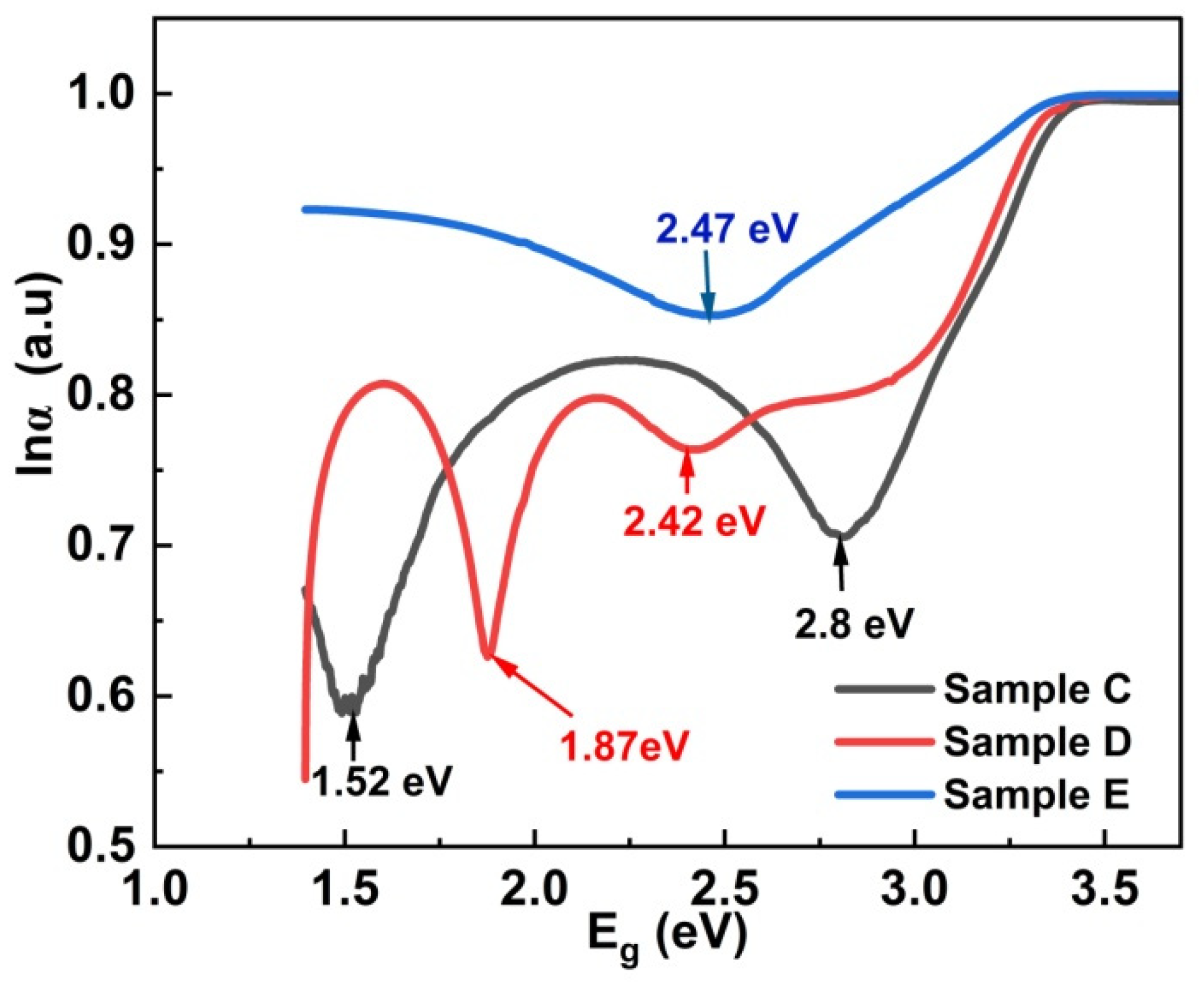
3.3. Optical Characterization
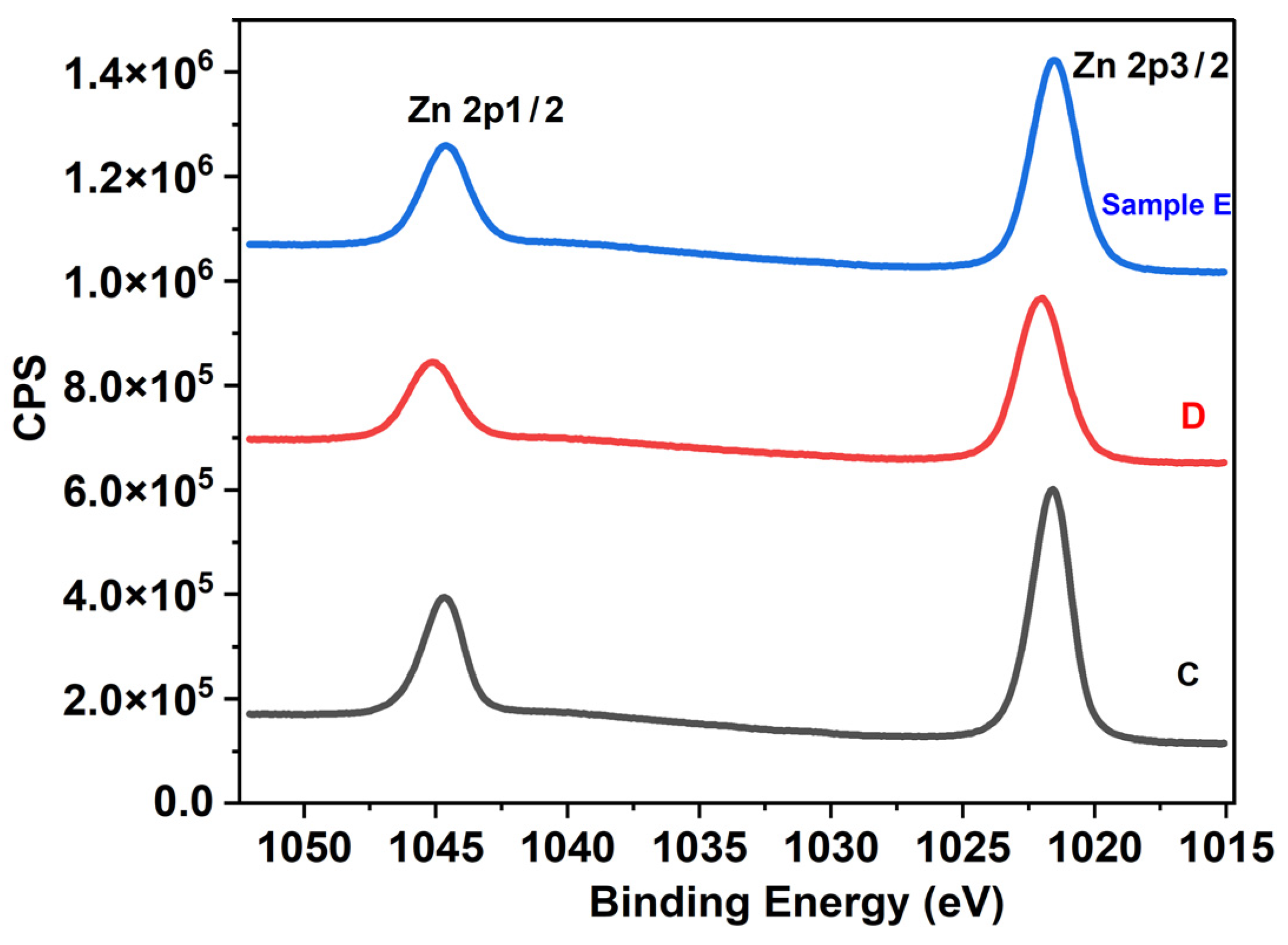
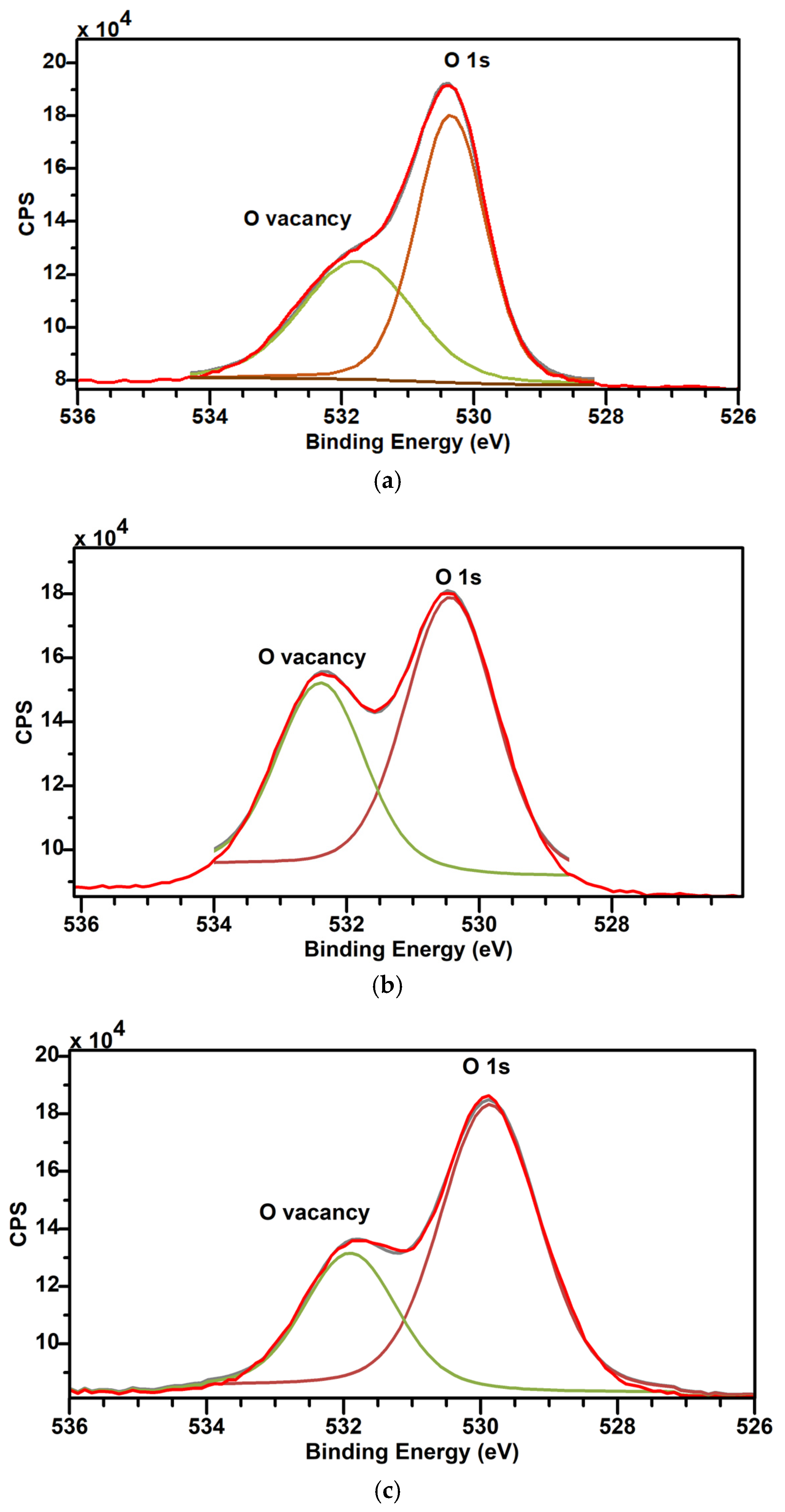
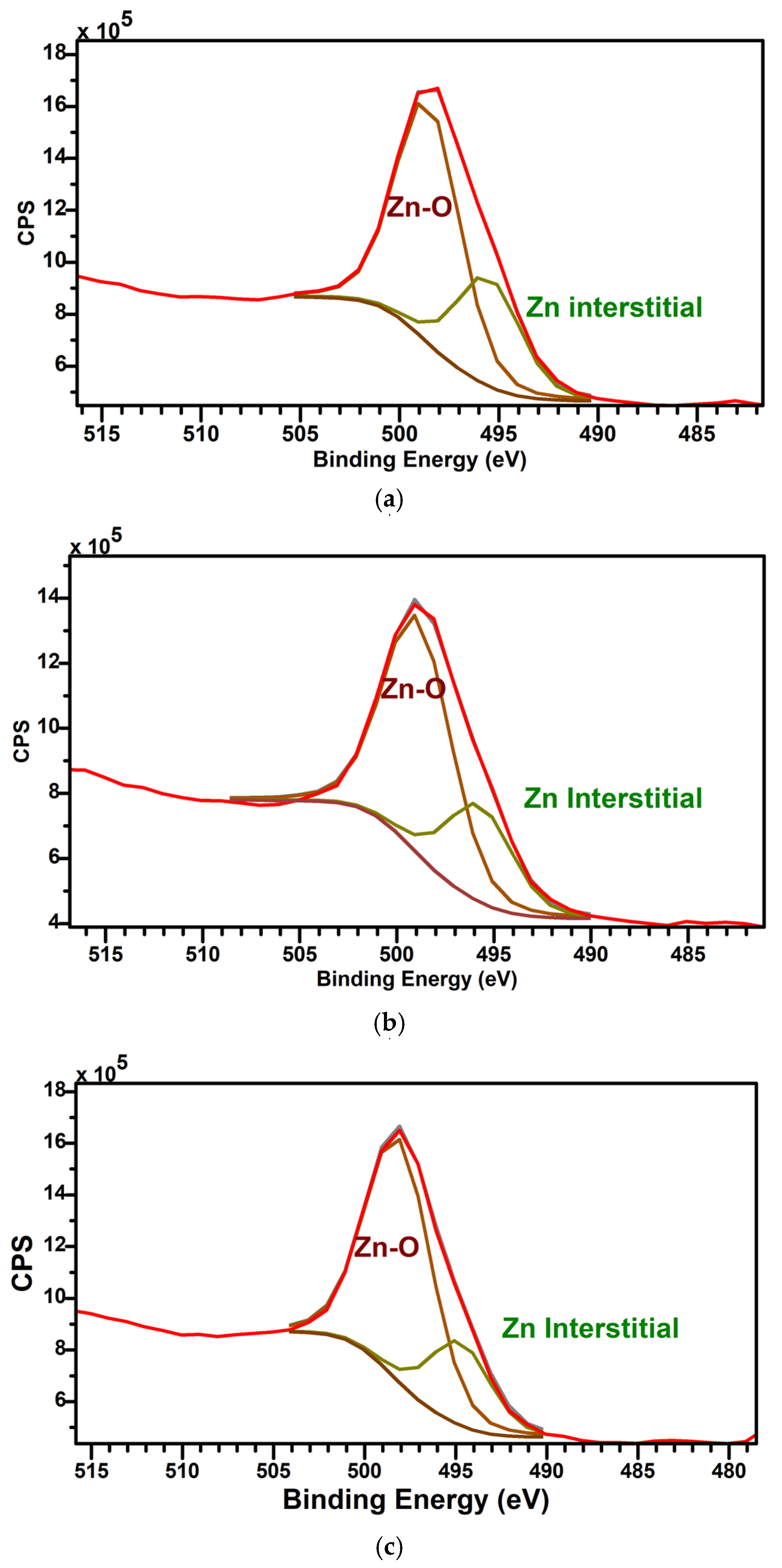
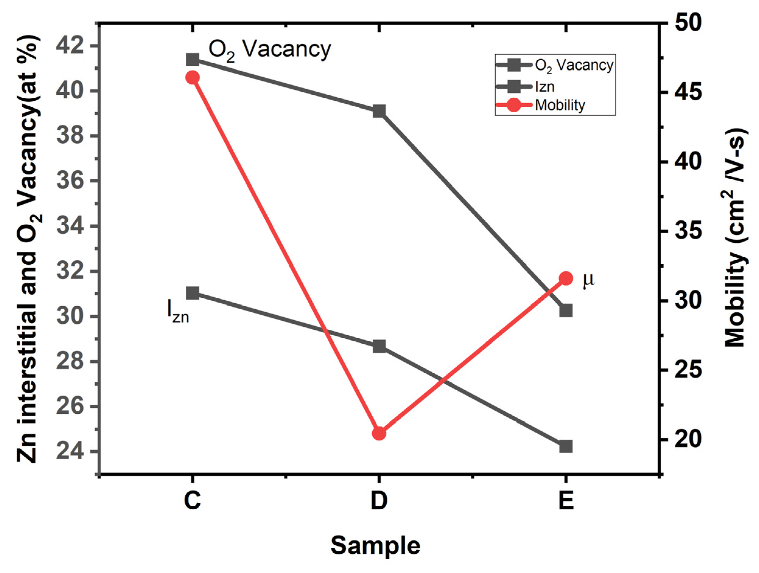
The Tauc plot between (αhν)2 and the bandgap (Eg) has been used to determine the absorption edge of the ZnO thin-film Samples C, D and E (Figure 5). All the Samples C, D and E show a bulk-like absorption edge, attesting to good-quality ZnO thin films. Sample C, deposited at RT, exhibits an absorption edge at 3.28 eV, whereas Sample D, deposited at 250 °C, shows a redshift in the bandgap of 3.25 eV. Sample E, deposited at 300 °C, shows a further redshift to 3.15 eV, which may be attributed to the increase in the crystallite size observed in the SEM image and XRD calculation [51].
Intrinsically, ZnO thin films have both oxygen vacancies and Zn interstitials exhibiting n-type conductivity [52]. The observed absorption spectra of our ZnO thin films can be separated into the following transitions: (i) ZnO band-to-band transition, (ii) transitions to localized band states (widely known as Urbach tails) and (iii) free carrier absorption [53]. There are several reports on Urbach tail states in ZnO thin films, due to structural disorders [54,55].
In order to delineate various sub-bands of our samples, a natural log of the absorption edge and the bandgap was plotted [56]. Figure 6 shows the plot between ln (α) and the bandgap for Samples C, D and E. Sample C exhibits two Urbach tails at 2.8 eV and 1.52 eV, whereas Sample D exhibits a weak band-tail at 2.42 eV and a strong band-tail state at 1.87 eV. All the above Urbach tails observed in Samples C and D are attributed to the presence of both oxygen vacancies and Zn interstitials creating deep donor and acceptor levels within the bandgap, leading to strong sub-band absorption. There have been previous reports on ZnO nanoparticles exhibiting photoluminescence (PL) emission at around 2.8 eV, and this was attributed to the transition between Zn interstitials (IZn) and the valance band. Our Sample C shows a similar Urbach tail at 2.8 eV; we attribute that to the presence of possible excess IZn. The fast roll-off in Sample C becomes a slow roll-off in Sample D, with a reduced absorption coefficient, which could be due to the possible variation in localized IZn. Additionally, Sample D exhibits a fast roll-off at 1.87 eV, which could be due to the possible transition between various localized defect states. Bandopadhyay et al. reported similar complexes of IZn below the conduction band (CB) and oxygen vacancies (VO) above the valance band (VB), with emissions at 1.7eV and 2 eV, respectively [57]. Hence, we speculate the presence of a sharp band-tail at 1.87 eV in Sample D is due to the transition between the IZn below the CB and VO above the VB. These are highly localized band-tail states because of the sharp roll-off observed. Lastly, Sample E shows band-to-band absorption at 3.14 eV and a weak Urbach tail at 2.47 eV representative of possible (i) direct band transition and (ii) band-to-tail transition, respectively. It is worth noting that there is an overall reduction in the absorption coefficient in Sample E coupled with a slow roll-off at 2.47 eV. The absence of a sharp roll-off in Sample E may attest to the annihilation of localized defects; however, shallow defect states at 2.47 eV continue to exist.

3.4. XPS

Atomic % concentrations of the Zn and O2 elements were determined from the XPS survey spectrum for Samples C, D and E and are listed in Table 4. Sample C exhibits the lowest O2% (19.07%), which increases to 32.53% in Sample D and 44.83% in Sample E. Alternatively, the atomic Zn % starts to decrease as the samples are deposited at higher temperatures (Samples D and E). Sample E, deposited at 300 °C, is observed to reach the ideal ~50:50 stoichiometric ratio of ZnO. The presence of Zn2+ states bounded by O2− states in all the samples is confirmed by the peak separation of 23.1 eV between the core levels, Zn 2p1/2 and Zn 2p3/2, as shown in Figure 7 [58].
The O 1s XPS peaks of various films are shown in Figure 8a–c and their binding energies are listed in Table 5. The O 1s peak has been resolved into two peaks at ~530 eV and ~532 eV, representative of the O 1s peak and oxygen vacancies, respectively. Sample C exhibits a narrower O 1s peak at 530.3 eV, and a broader O2 vacancy peak at 531.7 eV. Sample C shows a lower area (58.62%) under the O 1s curve, indicative of a lower O2 concentration, as compared to Samples D (60.9%) and E (69.74%), which were deposited at higher temperatures (Table 1). It may be noted that Sample C underwent post-deposition annealing at 300 °C in N2 ambient that would have led to the desorption of O from the surface with a relatively low O2 atomic % of 19.07% (Table 4), thereby creating a spike in O2 vacancies (41.38%), as listed in Table 5. The relatively higher strain of 0.001% (Table 3) in Sample C also attests to the broader O2 vacancy peak (FWHM of 1.99 eV in Table 5). Alternatively, Samples D and E exhibit a relatively broader O 1s peak, and narrower O2 vacancy peaks. In particular, Sample D shows a broad O 1s peak with an FHWM of 1.6 eV, suggesting the presence of O2 complexes in addition to the O2 vacancies. Based on the XPS O 1s data, it is clear that Sample E exhibits better O2 incorporation, with the area under the O 1s curve being the highest at 69.74%.
Figure 9a–c illustrate the deconvoluted Zn LMM Auger peaks of Samples C, D and E. The concentrations of Zn interstitials (IZn) are thus determined and listed in Table 6. The Auger peak at ~495 eV confirms the presence of IZn in the layers. Sample C, deposited at RT, exhibits a Zn-rich bulk with a high Zn atomic % of 73.56% (as illustrated in Table 4) and highest percentage of IZn (as listed in Table 6). A steady decrease in IZn has been observed as the deposition temperatures are increased to 250 °C and 300 °C (Samples D and E). We speculate that these IZn act as shallow donors, which become annihilated when the substrate temperatures are increased.
The voids in the SEM image (Figure 4c) and the presence of Urbach tails at 2.8 eV and 1.53 eV in the Tauc plot are clear evidence of high % IZn- and VO-related defects in Sample C due to room temperature deposition. Further annealing of Sample C at 300 °C also did not help in the annihilation of defects. Based on the XPS analysis, it is clear that higher deposition temperatures not only enhance the O2 incorporation, but also reduce IZn and VO (oxygen-related defects). Auger analyses of the Zn LMM peak confirm the lowest percentage of IZn (24.23%) in Sample E.
Figure 10 shows the changes in the IZn, VO and mobilities with respect to the deposition temperatures (Samples C, D and E). It is evident that both the atomic % of IZn and VO decreases as the deposition temperature increases. The changes in mobility can be explained in terms of variations in IZn and VO in the lattice. All our Hall measurements showed that the films are n-type, attested to by the presence of VO and IZn, or both. Sample C exhibits the highest mobility, which is one of the highest reported in the literature (Table 7). The observed drop in the mobility from Sample C to D shall be explained by the relatively high % of IZn (28.67% in Sample D), which may act as scattering sites. The SEM images and XRD results also attest to the degradation layer quality in Sample D when deposited at 250 °C. The SEM image shows the coalescing nature of ZnO, denoting the wrinkled nature of the sample (Figure 4d), and the GIXRD spectrum shows the polycrystalline property on the surface (Figure 3).
Finally, Sample E, deposited at 300 °C, shows an increase in the Hall mobility to 31.6 cm2/V-s. This shall be explained by the reduction in IZn (24.23%) and improvement in Zn-O bonding (75.77%) (Table 6). The results of the UV–Vis spectrum also show a slow roll-off in the Urbach tail at 2.47 eV, confirming the annihilation of localized defect states, which further explains the improvement in mobility for Sample E. We speculate the absence of localized defect states assists the increase in the mobility of Sample E, whereas the presence of localized defects at 1.87 eV in Sample D acts as traps, resulting in a reduction in mobility.

3.5. Device Characterization

Thin-film transistors were fabricated on 100 nm SiO2/Si substrates with a ZnO channel layer. TFT Device C1 was fabricated at room temperature followed by 300 °C post-deposition annealing (similar to Sample C thin film), whereas Devices D1 and E1 represent TFTs deposited at 250 °C and 300 °C, respectively. All the TFTs exhibit n-type behavior, as represented by the ID–VD curves. The drain current expressions for the enhancement-mode TFT are as follows:
Linear region
I D = W L C o x μ F E V G S V t h V D S 1 2 V D S 2
Saturation region
I D = W 2 L C o x μ F E V G S V t h 2
Expression for field-effect mobility (μFE):
μ F E = g m C o x W L V D S
S S = d V G S d log I D
where W—width of the channel, L—length of the channel, Cox—capacitance per unit area and gm—transconductance.

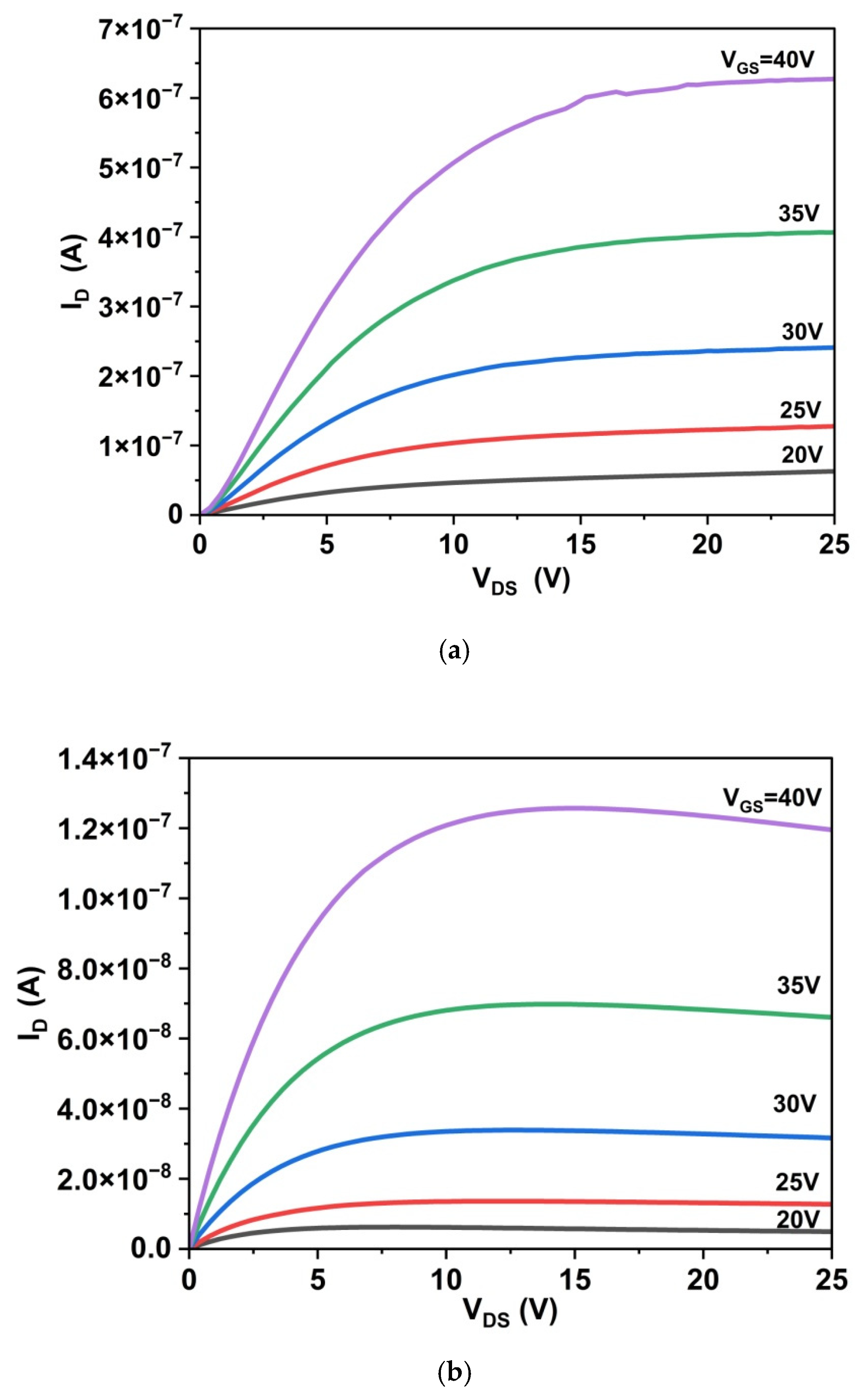
3.5.1. Drain Characteristics

The drain characteristics were measured for TFT devices with the same channel length and width of 50 μm. The gate–source voltage (VGS) is varied from 0 to 40 V in steps of 5 V. At VGS of 40 V, Device C1 reaches the highest drain current of 0.6 µA, whereas Devices D1 and E1 reach a maximum drain current of 0.11 µA. Variations in the drain currents match well with the variations in the bulk Hall mobility on Samples C, D and E, as represented in Table 8. Since the thickness of these devices is 180 nm, the bulk mobility dominates ID, where Sample C exhibits a highest Hall mobility of 46.09 cm2/V-s, corroborating with the high drain current of 0.6 µA in Device C1 (Figure 11a).

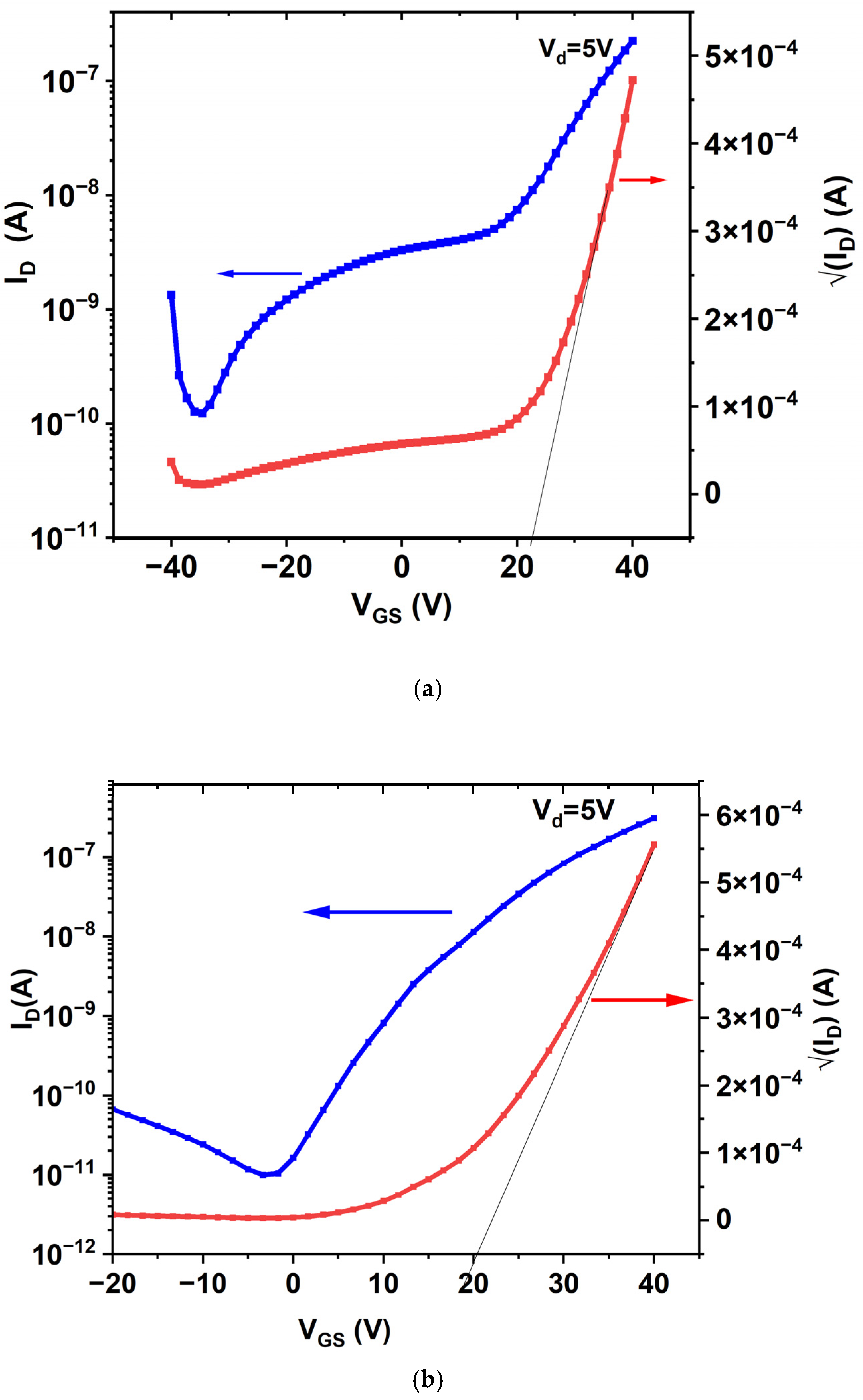
3.5.2. Transfer Characteristics

Figure 12a–c represent the transfer characteristics of the above TFT Devices C1, D1 and E1 at VDS = 5V. The gate voltage (VGS) is swept from −40 V to +40 V. The effect of the deposition temperature on the transfer curves shows that all the TFTs operate in the enhancement mode. Table 8 displays the electrical parameters of TFTs deposited at different temperatures. The IOFF current for Device C1 is of the order of nanoamperes (~1.2 × 10⁻¹⁰ A), indicative of a leaky device. The presence of voids between the crystallites observed in the SEM image, a smaller crystallite size (10.94 nm) and grain boundaries could be the reason for the nanoampere range leakage current in Sample C. Even though the bulk Hall mobility is determined to be the highest in Sample C, we speculate the high carrier concentration of 2.6 × 1017 cm−3 is predominantly defect-induced transport. The defect is confirmed by the presence of two localized band-tail states in the absorption data (Figure 6) at 1.53 eV and 2.8 eV. As the deposition temperature is increased to 250 °C and 300 °C in Devices D1 and E1, respectively, the leakage current substantially reduces to picoamperes of 9.96 × 10⁻¹² A and 9.35 × 10⁻¹² A, respectively.
Our thin-film investigation based on GIXRD and SEM analyses suggests that surface modifications happen when samples are deposited at higher temperatures of 250 °C and 300 °C. It may be noted that Devices D1 and E1 were subjected to oxygen over-pressure for ~2 h prior to breaking the vacuum. During the ramping down of the deposition temperature to RT, we speculate the surface layer is modified due to chemisorption of O2 atoms. The effect of chemisorption is also confirmed in our GIXRD data, where the intensity of the ZnO (103) peak is increased in Samples D and E. Our XPS analyses also support the theory of O2-rich layers in Samples D and E, where relatively high O 1s peaks are observed. Hence, the surface modification due to chemisorption is strongly believed to increase the crystallite size (13.83 nm and 11.38 nm) and reduce the grain boundaries and oxygen vacancies, which are combined indications of the reduced defects in high-temperature-deposited TFTs (D1 and E1).
The turn-ON voltage (VON) for Device C1 is measured at −34.6 V, and positively shifts to −3.33 V and 10.8 V in Devices D1 and E1, respectively. The decrease in IOFF, increase in VON voltage and high ION/IOFF ratio are clear evidence of the improved switching property for Devices D1 and E1 (Table 8). The shift in the VON is attributed to O2-rich thin films deposited at 300 °C, as also confirmed by the high O1s peak in the corresponding XPS spectrum (Figure 8a–c). Sangwon Lee et al. [72] similarly claimed in their InGaZnO TFTs that a shift in the turn-ON voltage is due to O2-rich layers.
Table 8 lists the field-effect mobility (µFE) and threshold voltage (VTh) values of Devices C1, D1 and E1. In general, the field-effect mobility and threshold voltage are inversely related in a ZnO deposition [73]. Device C1 exhibits the highest VTh of 23.1 V and lowest μFE, whereas Devices D1 and E1 exhibit a lower threshold voltage and higher field-effect mobility as compared to Device C1. Our XPS data confirm a higher incorporation of O2 at 32.53% and 44.84% in Devices D1 and E1, respectively, which explains our claim on VTh and μFE. In addition, the microstructure analyses of the SEM images show the presence of voids, which may act as charge trapping regions affecting the threshold voltage of Device C1. Further, a larger crystalline size of 13.858 nm and 11.385 nm in Devices D1 and E1, respectively, (Table 3) corroborating the larger crystallite size in the SEM images (Figure 4), explains the drop in the threshold voltage (VTh) and increase in the field-effect mobility (μFE).
Another parameter that defines the TFT performance is a sub-threshold swing (SS), which shows a decreasing trend from RT to high-temperature deposition. We propose the reason for the high SS in Sample C1 is due to O2 deficiency, leading to a nanoampere range of the leakage current. As the deposition temperature is further increased, O2-rich films in Devices D1 and E1 are the plausible reason for the lower leakage current, leading to lower values of SS.

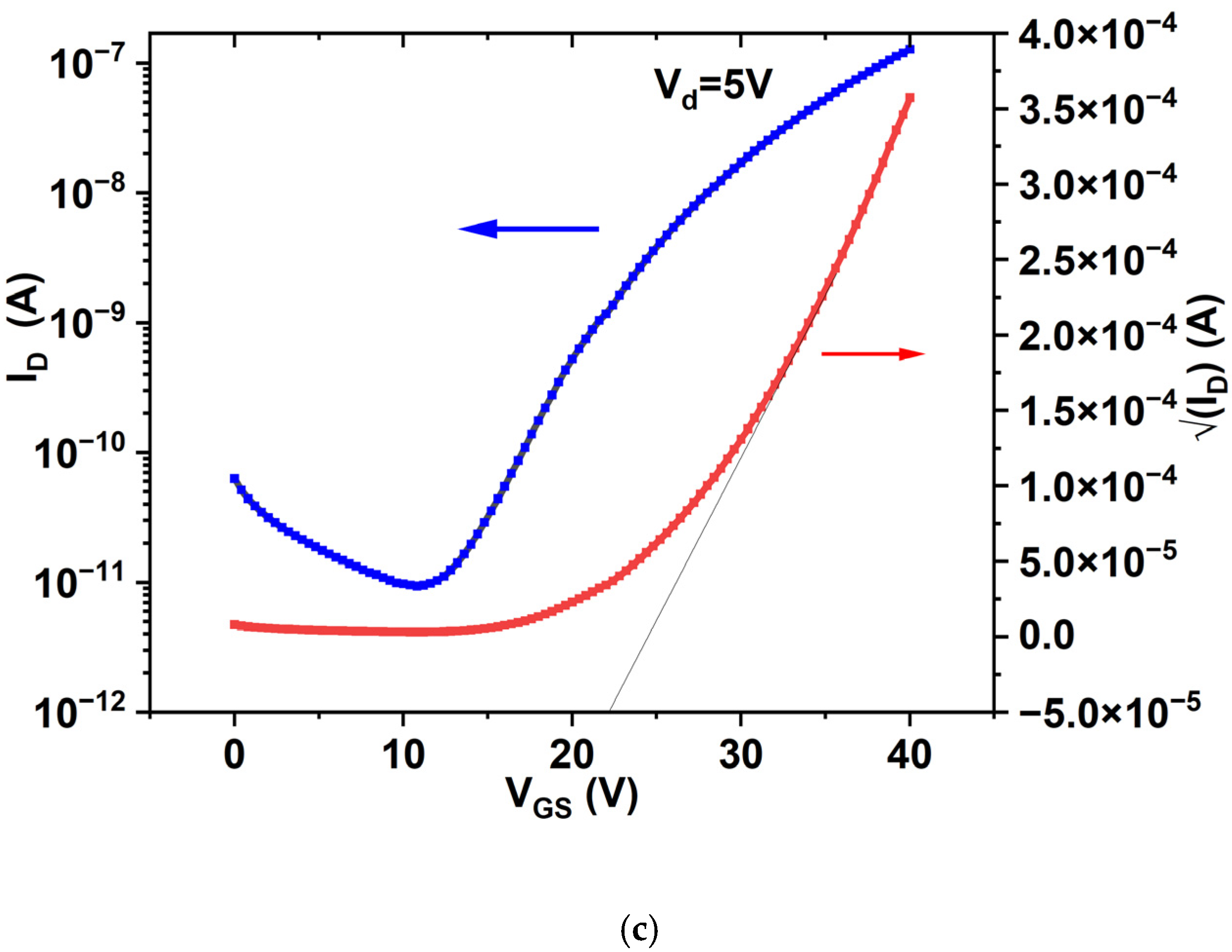
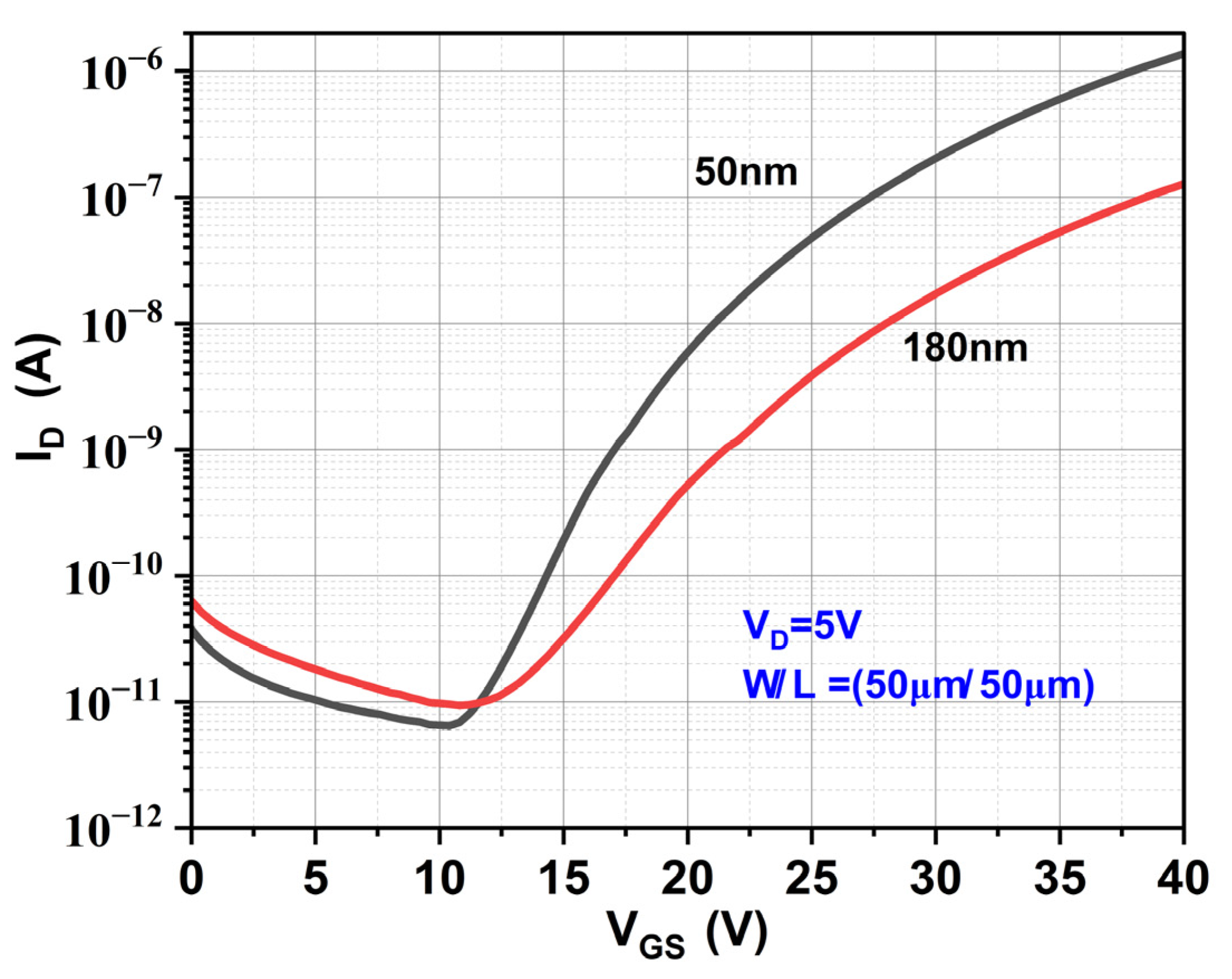
3.5.3. Variation in ZnO Layer Thickness

Figure 13 describes the transfer characteristics of ZnO TFTs with varying channel thicknesses of 180 nm and 50 nm, which represent Devices E1 and E2, respectively. Table 9 lists the variation in the TFT parameters for the 180 nm and 50 nm thick ZnO active layers. All other process parameters are unchanged except the ZnO thickness. Device E2 exhibits a lower leakage current compared to Device E1, which could be explained by the channel thickness being less than the width of the depletion layer, which was calculated using the following relation.
d c h < W d e p = 4 ε 0 ε r φ b q N e
where dch—channel thickness, Wdep—depletion width, εr—relative permittivity of ZnO, φb—for the potential gap between the Fermi level and intrinsic level, q—electron charge and Ne—carrier concentration.
A reduction in the channel thickness has increased the ION by 10-fold, leading to the improvement in the ION/IOFF ratio from 104 to 105. Consequently, the reduction in the sub-threshold slope is also observed in the thinner Device E2.

4. Conclusions

In conclusion, ZnO thin films deposited using RF sputtering were systematically optimized by varying the Ar:O2 gas flow rates and deposition temperatures. Structural, optical, microstructural and electrical properties were studied using XRD, a UV–visible spectrophotometer, XPS, Hall measurements and SEM imaging. The XRD results revealed polycrystalline properties on all the thin films. The UV–visible spectroscopy data showed a bulk-like absorption edge ranging from 3.28 eV to 3.17 eV, in addition to Urbach tail states within the bandgap. Thin films deposited at room temperature and annealed in N ambient resulted in low O2 incorporation, high oxygen vacancies and high Zn interstitials. From the absorption spectrum, we conclude that defects are highly localized in Sample C. Even though the films are deposited in an O2-rich environment, annealing in N ambient resulted in the desorption of O2 atoms from the surface, evident by the presence of voids in the corresponding SEM image. The Hall measurement derives a highest carrier mobility of 46.09 cm2/V-s in Sample C deposited at RT, possibly due to the high % of Zn interstitials. Deposition at 250 °C resulted in a polycrystalline top layer from the GIXRD, reduced % of oxygen vacancies and Zn interstitials confirmed by the XPS data and reduced band-tail states in the corresponding absorption spectrum, which explains the reduction in Hall mobility to 20.43 cm2/V-s. A further increase in the deposition temperature to 300 °C resulted in the overall improvement in the layer quality, attested to by the increase in the crystallite size from the XRD and SEM analyses, improvement in O2 incorporation and reduction in O2 vacancies and Zn interstitials from the XPS results, and substantial reduction in the localized Urbach tail from the absorption spectrum. Hence, based on the above analyses, ZnO thin film deposited at 300 °C seems to exhibit the best results even though a bulk mobility of 31.6 cm2/V-s has been obtained on Sample E.
Thin-film transistors with a W/L dimension of 50/50 µm were subsequently fabricated at RT, 250 °C and 300 °C. The device fabricated with RT deposition and 300 °C annealing resulted in a high leakage current (1.2 × 10⁻¹⁰ A) and high carrier concentration of 2.6 × 1017 cm−3, which are predominantly due to defect-induced transport. However, TFTs deposited at higher substrate temperatures of 250 °C and 300 °C showed a reduction in the leakage current (9.96 × 10⁻¹² A), threshold voltage (20.3 V), sub-threshold swing (4.43) and increase in the ION/IOFF ratio (104). A reduction in the ZnO layer thickness in the TFT at 300 °C ensured an O2-rich surface through chemisorption, leading to a reduction in the leakage current to 6.87 × 10⁻¹² A and sub-threshold swing to 2.8 V. Thus, these improvements in the TFT performance are governed by precise deposition process control such as the deposition temperature, ZnO layer thickness, towards the improvement in the crystalline quality, reduction in oxygen vacancies and Zn interstitial-related defects. From the above analyses, our optimal process parameter results have been obtained on 50 nm thick TFTs with a W/L dimension of 50/50 µm deposited at 300° C.

Supplementary Materials

The following supporting information can be downloaded at: https://www.mdpi.com/article/10.3390/ma17215153/s1, Figure S1: thin-film thickness measurement using Profilometer; Figure S2: image of the dark-field photomask used for channel creation and light-field photomask used for contact metallization; Figure S3: conventional XRD of ZnO thin film deposited at RT with different Ar:O2 flow rate; Figure S4: EDX analysis of ZnO thin films of Samples A, B, C; Table S1: elemental composition analysis of ZnO thin films.

Author Contributions

S.M.: methodology, conceptualization, software, formal analysis, investigation, data curation, writing—original draft preparation. S.B.: conceptualization, supervision, project administration, writing—review and editing. S.S.: validation, data curation. R.M.: resources, visualization. All authors have read and agreed to the published version of the manuscript.

Funding

This research work was carried out in the DST FIST-sponsored Interdisciplinary Nano Research Centre, Sri Venkateswara College of Engineering, Sriperumbudur. Thin-film characterization of the research work was performed using facilities at CeNSE, located at the Indian Institute of Science, Bengaluru. Device fabrication was performed using facilities at CNNP, IIT Madras as part of the Indian Nanoelectronics User Program (INUP-i2i), supported by the Ministry of Electronics and Information Technology (MeitY), Government of India.

Institutional Review Board Statement

Not applicable.

Informed Consent Statement

Not applicable.

Data Availability Statement

The original contributions presented in the study are included in the article/Supplementary Materials, further inquiries can be directed to the corresponding author.

Conflicts of Interest

The authors declare no conflicts of interest.

References

  1. Shen, L.; Ma, Z.Q.; Shen, C.; Li, F.; He, B.; Xu, F. Studies on fabrication and characterization of a ZnO/p-Si-based solar cell. Superlattices Microstruct. 2010, 48, 426–433. [Google Scholar] [CrossRef]
  2. Wong, T.K.S.; Zhuk, S.; Masudy-Panah, S.; Dalapati, G.K. Current Status and Future Prospects of Copper Oxide Heterojunction Solar Cells. Materials 2016, 9, 271. [Google Scholar] [CrossRef] [PubMed]
  3. Bouras, K.; Schmerber, G.; Rinnert, H.; Aureau, D.; Park, H.; Ferblantier, G.; Colis, S.; Fix, T.; Park, C.; Kim, W.K.; et al. Structural, optical and electrical properties of Nd-doped SnO2 thin films fabricated by reactive magnetron sputtering for solar cell devices. Sol. Energy Mater. Sol. Cells 2016, 145, 134–141. [Google Scholar] [CrossRef]
  4. Saim, H.B.; Campbell, D.S. Properties of indium-tin-oxide (ITO)/silicon heterojunction solar cells by thick-film techniques. Sol. Energy Mater. 1987, 15, 249–260. [Google Scholar] [CrossRef]
  5. Guo, D.; Zhuo, M.; Zhang, X.; Xu, C.; Jiang, J.; Gao, F.; Wan, Q.; Li, Q.; Wang, T. Indium-tin-oxide thin film transistor biosensors for label-free detection of Avian influenza virus H5N1. Anal. Chim. Acta 2013, 773, 83–88. [Google Scholar] [CrossRef]
  6. Amutha Surabi, M.; Chandradass, J.; Park, S.J. ZnO-Based Thin Film Transistor Fabricated Using Radio Frequency Magnetron Sputtering at Low Temperature. Mater. Manuf. Process. 2015, 30, 175–178. [Google Scholar] [CrossRef]
  7. Presley, R.E.; Munsee, C.L.; Park, C.-H.; Hong, D.; Wager, J.F.; Keszler, D.A. Tin oxide transparent thin-film transistors. J. Phys. D Appl. Phys. 2004, 37, 2810–2813. [Google Scholar] [CrossRef]
  8. Al-Jawhari, H.A. A review of recent advances in transparent p-type Cu2O-based thin film transistors. Mater. Sci. Semicond. Process. 2015, 40, 241–252. [Google Scholar] [CrossRef]
  9. Zhai, T.; Fang, X.; Liao, M.; Xu, X.; Zeng, H.; Yoshio, B.; Golberg, D. A comprehensive review of one-dimensional metal-oxide nanostructure photodetectors. Sensors 2009, 9, 6504–6529. [Google Scholar] [CrossRef]
  10. Liang, S.; Sheng, H.; Liu, Y.; Huo, Z.; Lu, Y.; Shen, H. ZnO Schottky ultraviolet photodetectors. J. Cryst. Growth 2001, 225, 110–113. [Google Scholar] [CrossRef]
  11. Liu, X.; Du, H.; Wang, P.; Lim, T.-T.; Sun, X.W. A high-performance UV/visible photodetector of Cu2O/ZnO hybrid nanofilms on SWNT-based flexible conducting substrates. J. Mater. Chem. C 2014, 2, 9536–9542. [Google Scholar] [CrossRef]
  12. Nath, A.; Mahajan, B.K.; Singh, L.R.; Shubhajit, V.; Rajib Kumar, N.; Mitra, B.S. Enhancing Detectivity of Indium-Oxide-Based Photodetectors via Vertical Nano structuring Through Glancing Angle Deposition. J. Electron. Mater. 2021, 50, 3722–3730. [Google Scholar] [CrossRef]
  13. Oruc, F.B.; Cimen, F.; Rizk, A.; Ghaffari, M.; Nayfeh, A.; Okyay, A.K. Thin-Film ZnO Charge-Trapping Memory Cell Grown in a Single ALD Step. IEEE Electron. Device Lett. 2012, 33, 1714–1716. [Google Scholar] [CrossRef]
  14. Kumar, D.; Aluguri, R.; Chand, U.; Tseng, T.Y. Metal oxide resistive switching memory: Materials, properties and switching mechanisms. Ceram. Int. 2017, 43, 547–556. [Google Scholar] [CrossRef]
  15. Nath, A.; Mahajan, B.K.; Sarkar, M.B. Ag Nanoparticles Sheltered In2O3 Nanowire as a Capacitive MOS Memory Device. IEEE Trans. Nanotechnol. 2020, 19, 856–863. [Google Scholar]
  16. Mishra, S.; Ghanshyam, C.; Ram, N.; Bajpai, R.P.; Bedi, R.K. Detection mechanism of metal oxide gas sensor under UV radiation. Sens. Actuators B Chem. 2004, 97, 387–390. [Google Scholar] [CrossRef]
  17. Hendi, A.A.; Alorainy, R.H. New fabrication of zinc oxide nanostructure thin film gas sensors. Superlattices Micro Struct. 2014, 66, 23–32. [Google Scholar] [CrossRef]
  18. Lin, C.-W.; Chen, H.-I.; Chen, T.-Y.; Huang, C.-C.; Hsu, C.-S.; Liu, R.-C.; Liu, W.-C. On an indium–tin-oxide thin film based ammonia gas sensor. Sens. Actuators B Chem. 2011, 160, 1481–1484. [Google Scholar] [CrossRef]
  19. Xu, J.C.; Hunter, G.W.; Lukco, D.; Liu, C.-C.; Ward, B.J. Novel Carbon Dioxide Micro sensor Based on Tin Oxide Nanomaterial Doped With Copper Oxide. IEEE Sens. J. 2009, 9, 235–236. [Google Scholar] [CrossRef]
  20. Şerban, I.; Enesca, A. Metal Oxides-Based Semiconductors for Biosensors Applications. Front. Chem. 2020, 8, 354. [Google Scholar] [CrossRef]
  21. Jindal, K.; Tomar, M.; Gupta, V. CuO thin film based uric acid biosensor with enhanced response characteristics. Bio Sens. Bio Electron. 2012, 38, 11–18. [Google Scholar] [CrossRef] [PubMed]
  22. Batra, N.; Tomar, M.; Gupta, V. Efficient detection of cholesterol using ZnO thin film based matrix. J. Exp. Nanosci. 2012, 8, 280–287. [Google Scholar] [CrossRef]
  23. Chiu, I.-C.; Li, Y.-S.; Tu, M.-S.; Cheng, I.-C. Complementary Oxide–Semiconductor-Based Circuits with n-Channel ZnO and p- Channel SnO Thin-Film Transistors. IEEE Electron. Device Lett. 2014, 35, 1263–1265. [Google Scholar] [CrossRef]
  24. Shijeesh, M.R.; Mohan, P.A.; Jayaraj, M.K. Complementary Inverter Circuits Based on p-Cu2O and n-ZTO Thin Film Transistors. J. Electron. Mater. 2020, 49, 537–543. [Google Scholar] [CrossRef]
  25. Peng, W.; Mao, K.; Cai, F.; Meng, H.; Zhu, Z.; Li, T.; Yuan, S.; Xu, Z.; Feng, X.; Xu, J.; et al. Reducing non radiative recombination in perovskite solar cells with a porous insulator contact. Science 2023, 379, 683–690. [Google Scholar] [CrossRef]
  26. Davis, K.; Yarbrough, R.; Froeschle, M.; White, J.; Rathnayake, H. Band gap engineered zinc oxide nanostructures via a sol–gel synthesis of solvent driven shape-controlled crystal growth. RSC Adv. 2019, 9, 14638–14648. [Google Scholar] [CrossRef]
  27. Biggs, J.; Myers, J.; Kufel, J.; Ozer, E.; Craske, S.; Sou, A.; Ramsdale, C.; Williamson, K.; Price, R.; White, S. A natively flexible 32-bit Arm microprocessor. Nature 2021, 595, 532–536. [Google Scholar] [CrossRef]
  28. Yuvaraja, S.; Faber, H.; Kumar, M.; Na, X.; García, G.I.M.; Tang, X.; Anthopoulos, T.D.; Li, X. Three-dimensional integrated metal-oxide transistors. Nat. Electron. 2024, 7, 768–776. [Google Scholar] [CrossRef]
  29. Kamaruddin, S.A.; Chan, K.Y.; Yow, H.K. Zinc oxide films prepared by sol–gel spin coating technique. Appl. Phys. A 2011, 104, 263–268. [Google Scholar] [CrossRef]
  30. Ortel, M.; Balster, T.; Wagner, V. Chemical composition and temperature dependent performance of ZnO-thin film transistors deposited by pulsed and continuous spray pyrolysis. J. Appl. Phys. 2013, 114, 234502. [Google Scholar] [CrossRef]
  31. Saha, J.K.; Bukke, R.N.; Mude, N.N.; Jang, J. Significant improvement of spray pyrolyzed ZnO thin film by precursor optimization for high mobility thin film transistors. Sci. Rep. 2020, 10, 8999. [Google Scholar] [CrossRef] [PubMed]
  32. Gupta, M.; Chowdhury, F.R.; Barlage, D.; Tsui, Y.Y. Optimization of pulsed laser deposited ZnO thin-film growth parameters for thin-film transistors (TFT) application. Appl. Phys. A 2013, 110, 793–798. [Google Scholar] [CrossRef]
  33. Zhang, X.-A.; Zhang, J.-W.; Zhang, W.-F.; Wang, D.; Bi, Z.; Bian, X.-M.; Hou, X. Enhancement-mode thin film transistor with nitrogen-doped ZnO channel layer deposited by laser molecular beam epitaxy. Thin Solid Film. 2008, 516, 3305–3308. [Google Scholar] [CrossRef]
  34. Tampo, H.; Shibata, H.; Maejima, K.; Yamada, A.; Matsubara, K.; Fons, P.; Kashiwaya, S.; Niki, S.; Chiba, Y.; Wakamatsu, T.; et al. Polarization-induced two-dimensional electron gases in ZnMgO/ZnO heterostructures. Appl. Phys. Lett. 2008, 93, 202104. [Google Scholar] [CrossRef]
  35. Li, H.; Han, D.; Yi, Z.; Dong, J.; Zhang, S.; Zhang, X.; Wang, Y. High-Performance ZnO Thin-Film Transistors Prepared by Atomic Layer Deposition. IEEE Trans. Electron. Devices 2019, 66, 2965–2970. [Google Scholar] [CrossRef]
  36. Carcia, P.F.; McLean, R.S.; Reilly, M.H. High-performance ZnO thin-film transistors on gate dielectrics grown by atomic layer deposition. Appl. Phys. Lett. 2006, 88, 123509. [Google Scholar] [CrossRef]
  37. Navamathavan, R.; Choi, C.K.; Park, S.-J. Electrical properties of ZnO-based bottom-gate thin film transistors fabricated by using radio frequency magnetron sputtering. J. Alloys Compd. 2009, 475, 889–892. [Google Scholar] [CrossRef]
  38. Singh, S.; Chakrabarti, P. Simulation, fabrication and characterization of ZnO based thin film transistors grown by radio frequency magnetron sputtering. J. Nanosci. Nanotechnol. 2012, 12, 1880–1885. [Google Scholar] [CrossRef]
  39. Lee, J.H.; Kim, H.S.; Kim, S.H.; Jang, N.W.; Yun, Y. Characterization of magnesium oxide gate insulators grown using RF sputtering for ZnO thin-film transistors. Curr. Appl. Phys. 2014, 14, 794–797. [Google Scholar] [CrossRef]
  40. Medina-Montes, M.I.; Lee, S.H.; Pérez, M.; Baldenegro-Pérez, L.A.; Quevedo-López, M.A.; Gnade, B.; Ramírez-Bon, R. Effect of Sputtered ZnO Layers on Behavior of Thin-Film Transistors Deposited at Room Temperature in a Nonreactive Atmosphere. J. Electron. Mater. 2011, 40, 1461–1469. [Google Scholar] [CrossRef]
  41. Kandpal, K.; Gupta, N. Perspective of zinc oxide based thin film transistors: A comprehensive review. Microelectron. Int. 2018, 35, 52–63. [Google Scholar] [CrossRef]
  42. Park, J.; Rim, Y.S.; Li, C.; Kim, H.-S.; Goorsky, M.; Streit, D. Deep-level defect distribution as a function of oxygen partial pressure in sputtered ZnO thin-film transistors. Curr. Appl. Phys. 2016, 16, 1369–1373. [Google Scholar] [CrossRef]
  43. Kamiya, T.; Nomura, K.; Hosono, H. Present status of amorphous In–Ga–Zn–O thin-film transistors. Sci. Technol. Adv. Mater. 2010, 11, 044305. [Google Scholar] [CrossRef]
  44. Walker, B.; Pradhan, A.K.; Xiao, B. Low temperature fabrication of high performance ZnO thin film transistors with high-k dielectrics. Solid State Electron. 2015, 111, 58–61. [Google Scholar] [CrossRef]
  45. Wang, B.-S.; Li, Y.-S.; Cheng, I.-C. Mobility Enhancement in RF-Sputtered MgZnO/ZnO Heterostructure Thin-Film Transistors. IEEE Trans. Electron. Devices 2016, 63, 1545–1549. [Google Scholar] [CrossRef]
  46. Vyas, S.; Dwivedi, A.D.D.; Dwivedi, R.D. Effect of gate dielectric on the performance of ZnO based thin film transistor. Superlattices Microstruct. 2018, 120, 223–234. [Google Scholar] [CrossRef]
  47. Amitabha, N.; Bikram, K.M.; Aniruddha, M.; Laishram, R.S.; Mitra, B.S. Synthesis and detailed characterizations of Ag nanoparticles coated In2O3 nanostructured devices: An analytical and experimental approach. J. Vac. Sci. Technol. B 2021, 39, 052209. [Google Scholar]
  48. Wang, Y.; Li, X.; Jiang, G.; Liu, W.; Zhu, C. Origin of (103) plane of ZnO films deposited by RF magnetron sputtering. J. Mater. Sci. Mater. Electron. 2013, 24, 3764–3767. [Google Scholar] [CrossRef]
  49. Prasad, B.E.; Kamath, P.V. Electrochemical synthesis of ZnO coatings from water–isopropanol mixed baths: Control over oriented crystallization. J. Solid State Electro Chem. 2010, 14, 2083–2088. [Google Scholar] [CrossRef]
  50. Lin, K.M.; Chen, Y.Y.; Chou, K.Y. Solution derived Al-doped zinc oxide films: Doping effect, microstructure and electrical property. J. Sol.-Gel Sci. Technol. 2009, 49, 238–242. [Google Scholar] [CrossRef]
  51. Mandal, S.; Singha, R.K.; Dhar, A.; Ray, S.K. Optical and structural characteristics of ZnO thin films grown by RF magnetron sputtering. Mater. Res. Bull. 2008, 43, 244–250. [Google Scholar] [CrossRef]
  52. Kavindra, K.; Gupta, N.; Singh, J.; Shekhar, C. On the Threshold Voltage and Performance of ZnO- Based Thin-Film Transistors with a ZrO2 Gate Dielectric. J. Electron. Mater. 2020, 49, 3156–3164. [Google Scholar]
  53. Urbach, F. The Long-Wavelength Edge of Photographic Sensitivity and of the Electronic Absorption of Solids. Phys. Rev. 1953, 92, 1324. [Google Scholar] [CrossRef]
  54. Kröger, F.A. The Chemistry of Imperfect Crystals, 2nd ed.; North-Holland Publishing Company Inc.: Amsterdam, The Netherlands, 1974. [Google Scholar]
  55. Egelhaaf, H.-J.; Oelkrug, D. Luminescence and nonradiative deactivation of excited states involving oxygen defect centers in polycrystalline ZnO. J. Cryst. Growth 1996, 161, 190–194. [Google Scholar] [CrossRef]
  56. Sinthamani, S.; Ranjithkumar, M.; Sudhakar, K.B.; Anitha, S.; Sudharsanam, S.; Sasikala, M. Optical characterization of RF sputtered copper oxide for thin film solar cell applications. Mater. Today Proc. 2022, 59, 814–818. [Google Scholar] [CrossRef]
  57. Bandopadhyay, K.; Mitra, J. Zn interstitials and O vacancies responsible for n-type ZnO: What do the emission spectra reveal? RSC Adv. 2015, 5, 23540–23547. [Google Scholar] [CrossRef]
  58. Pandey, S.K.; Pandey, S.K.; Mukherjee, C.; Mishra, P.; Gupta, M.; Barman, S.R.; D’Souza, S.W.; Mukherjee, S. Effect of growth temperature on structural, electrical and optical properties of dual ion beam sputtered ZnO thin films. J. Mater. Sci. Mater. Electron. 2013, 24, 2541–2547. [Google Scholar] [CrossRef]
  59. Tsakonas, C.; Kuznetsov, V.L.; Cranton, W.M.; Kalfagiannis, N.; Abusabee, K.M.; Koutsogeorgis, D.C.N.; Abeywickrama, N.; Edwards, P.P. Low temperature sputter-deposited ZnO films with enhanced Hall mobility using excimer laser post-processing. J. Phys. D Appl. Phys. 2017, 50, 485306. [Google Scholar] [CrossRef]
  60. Kim, J.-H.; Koo, S.-M. Epitaxial ZnO thin film transistors on 4H-SiC substrates. Ceram. Int. 2015, 41, 14641–14644. [Google Scholar] [CrossRef]
  61. Naeem-ur-Rehman Khan, H.; Mehmood, M.; Ling, F.C.C.; Faheem Khan, A.; Ali, S.M. Comparative Study on Structural, Optical, and Electrical Properties of ZnO Thin Films Prepared by PLD and Sputtering Techniques. Semiconductors 2020, 54, 999–1010. [Google Scholar] [CrossRef]
  62. Wu, Y.; Cao, F.; Ji, X. Optical and electrical properties of Al-doped ZnO thin films by atomic layer deposition. J. Mater. Sci. Mater. Electron. 2020, 31, 17365–17374. [Google Scholar] [CrossRef]
  63. Hanna, B.; Manuraj, M.; Surendran, K.P.; Narayanan Unni, K.N. Opto-electronic properties of solution-processed zinc oxide thin films: Role of solvents and doping. J. Mater. Sci. Mater. Electron. 2020, 31, 13570–13577. [Google Scholar] [CrossRef]
  64. Gremenok, V.F.; Ivanov, V.A.; Petlitskii, A.N.; Petlitskaya, T.V.; Suleymanov, S.K.; Dyskin, V.G.; Djanklich, M.U.; Kulagina, N.A. ZnO Films Obtained by Reactive Magnetron Sputtering: Microstructure, Electrical, and Optical Characteristics. Appl. Sol. Energy 2020, 56, 186–191. [Google Scholar] [CrossRef]
  65. Wang, Z.W.; Zang, H.; Ren, L.Y. Influence of annealing temperature on structural, electrical and optical properties of undoped zinc oxide thin films. J. Mater. Sci. Mater. Electron. 2014, 25, 5422–5427. [Google Scholar] [CrossRef]
  66. Han, D.; Wang, Y.; Zhang, S.; Lei, S.; Han, R.; Matsumoto, S.; Ino, Y. Influence of sputtering power on properties of ZnO thin films fabricated by RF sputtering in room temperature. Sci. China Inf. Sci. 2011, 55, 951–955. [Google Scholar] [CrossRef]
  67. Prasada Rao, T.; Santhosh Kumar, M.C.; Ganesan, V. Effect of annealing on the structural, optical and electrical properties of ZnO thin films by spray pyrolysis. Indian J. Phys. 2011, 85, 1381–1391. [Google Scholar] [CrossRef]
  68. Varma, T.; Periasamy, C.; Boolchandani, D. Performance evaluation of bottom gate ZnO based thin film transistors with different W/L ratios for UV sensing. Superlattices Microstruct. 2018, 114, 284–295. [Google Scholar] [CrossRef]
  69. Mohamed, A.H.; Ghazali, N.A.B.; Chong, H.M.H.; Cobley, R.J.; Li, L.; Kalna, K. Channel mobility and contact resistance in scaled ZnO thin-film transistors. Solid State Electron. 2020, 172, 107867. [Google Scholar] [CrossRef]
  70. Yoon, M. Subthreshold Conduction of Disordered ZnO-Based Thin-Film Transistors. Micromachines 2023, 14, 1596. [Google Scholar] [CrossRef]
  71. Alharbi, A.G.; Shafi, N. Design, fabrication and characterization of circular ZnO TFT for UV detection applications. Microelectron. J. 2023, 131, 105648. [Google Scholar] [CrossRef]
  72. Lee, S.; Park, J.; Yang, G.W.; Kim, C.W.; Choi, S.-J.; Kim, D.M.; Bae, J.-H.; Kim, D.H. Analysis of a-InGaZnO TFT Threshold Voltage Instability and Mobility Boosting by Current Stress at a Cryogenic Temperature. IEEE Electron. Device Lett. 2023, 44, 88–91. [Google Scholar] [CrossRef]
  73. Medina-Montes, M.I.; Baldenegro-Perez, L.A.; Sanchez-Zeferino, R.; Rojas-Blanco, L.; Becerril-Silva, M.; Quevedo-Lopez, M.A.; Ramirez-Bon, R. Effect of depth of traps in ZnO polycrystalline thin films on ZnO-TFTs performance. Solid-State Electron. 2016, 123, 119–123. [Google Scholar] [CrossRef]
Figure 1. Schematic structure of ZnO TFT.
Materials 17 05153 g001
Figure 2. GIXRD spectra of ZnO thin-film Samples A, B and C with different Ar:O2 flow rates.
Materials 17 05153 g002
Figure 3. GIXRD spectra of samples with different substrate temperatures.
Materials 17 05153 g003
Figure 4. SEM image of ZnO thin-film Samples (a) A, (b) B, (c) C (Red arrows represents small voids between the crystallites), (d) D and (e) E.
Materials 17 05153 g004
Figure 5. Tauc plot of Samples C, D and E.
Materials 17 05153 g005
Figure 6. ln α vs. energy bandgap (Eg).
Materials 17 05153 g006
Figure 7. Core-level spectrum of Zn 2P peak.
Materials 17 05153 g007
Figure 8. (a) XPS spectrum of O 1s peak—Sample C. (b) XPS spectrum of O 1s peak—Sample D. (c) XPS spectrum of O 1s peak—Sample E, with the following color representations: Red—Original XPS data, Green—O Vacancies component and Burgundy—O 1s peak component.
Materials 17 05153 g008
Figure 9. (a) Zn LMM Auger peak—Sample C. (b) Zn LMM Auger peak—Sample D. (c) Zn LMM Auger peak—Sample E, with the following color representations: Red—Original XPS data, Green—Zn interstitials component and Burgundy—Zn-O component.
Materials 17 05153 g009
Figure 10. Plot of Zn interstitials, O2 vacancy and mobility of ZnO thin films.
Materials 17 05153 g010
Figure 11. (a) Drain characteristics of TFT Device C1. (b) Drain characteristics of TFT Device D1. (c) Drain characteristics of TFT Device E1.
Materials 17 05153 g011aMaterials 17 05153 g011b
Figure 12. (a) Transfer characteristics of TFT Device C1. (b) Transfer characteristics of TFT Device D1. (c) Transfer characteristics of TFT Device E1.
Materials 17 05153 g012aMaterials 17 05153 g012b
Figure 13. Transfer characteristics of ZnO TFT with variation in channel layer thickness.
Materials 17 05153 g013
Table 1. Deposition parameters of ZnO thin films.
SampleDeposition TemperatureAr:O2
Flow Rate
Annealing
Temperature and Duration
RF Power
ART20:0N2
ambient 300 °C, 30 min
60 W
BRT18:2
CRT16:4
D250 °C16:4-------60 W
E300 °C16:4
Table 2. Deposition parameters and Hall performance of ZnO TFT.
SampleDeposition TemperatureAnnealing Temperature and AmbientAr:O2
Flow Rate
Post-Contact AnnealingCarrier Concentration (cm−3)
C1RT300 °C in N2 ambient16:4220 °C2.6 × 1017
D1250 °C-1 × 10¹⁶
E1300 °C-1.6 × 10¹⁷
Table 3. ZnO thin-film parameters extracted from XRD.
SampleFWHM (β)
(Radians)

(Deg)
Crystallite
Size D (nm)
Dislocation
Density δ
(Lines/m2)
Lattice
Parameter Spacing (nm)
Micro-Strain ε
A0.5734.5314.5960.00470.2600.0008
B0.734.2511.8760.00710.2620.0009
C0.7634.310.9400.00840.2610.0010
D0.634.3113.8580.00520.2610.0008
E0.7334.1511.3850.00770.2620.0010
Table 4. Atomic % calculation from XPS survey spectrum.
ElementCDE
O 1s19.0732.5344.84
Zn 2p73.5656.7647.66
C7.3610.717.5
Table 5. Oxygen vacancies obtained from XPS.
SampleO2 VacancyO 1s Peak
Binding Energy (eV)% ConcFWHMBinding Energy (eV)FWHM% Conc
C531.7741.381.99530.3541.2558.62
D532.3839.11.54530.431.660.9
E531.8830.261.57529.881.769.74
Table 6. Deconvolution and % concentration of Zn-O and Zn interstitials from Zn Auger LMM peak.
CDE
Zn-O 68.9771.3375.77
Zn Interstitials31.0328.6724.23
Table 7. Comparison of ZnO thin-film electrical properties with the literature.
YearDeposition MethodMobility
(cm2/V-s)
Carrier Concentration (cm−3)Resistivity
(Ω-cm)
2017 [59]Sputtering17.3 2.3 × 10¹⁸-
2015 [60]Sputtering24.176.21 × 1015-
2020 [61]Pulsed Laser Deposition34.62.28 × 10180.0792
2020 [62]Atomic Layer Deposition17.364.32 × 10208.33 × 10–4
2020 [63]Sol–gel0.051.2 × 1015-
2020 [64]Sputtering18-3 × 10⁻⁴
2014 [65]Sputtering0.0641.4 × 10196.8
2011 [66]Sputtering349.29 × 10111.98 × 105
2011 [67]Spray pyrolysis0.267.27 × 10153.20 × 103
2011 [40]Sputtering8.94.2 × 101631.8
This workSputtering46.092.6 × 10171.96
TFT
2018 [46]Sputtering 0.7 *--
2018 [68]Sputtering0.62 *--
2020 [69]Plasma ALD0.782 *--
2023 [70]ALD3.1 *--
2023 [71]Sputtering0.08 *--
This workSputtering1.1 *--
* Field-effect mobility of TFT.
Table 8. Electrical parameters of TFTs deposited at different temperatures.
SampleBulk Mobility (cm2/V-s)ION
(μA)
VON
(V)
VTh
(V)
SS
(V/dec)
ION/IOFF RatioμFE
(cm2/V-s)
C146.090.223−34.623.1301030.062
D120.431.58−3.3320.36.611040.64
E131.60.12710.821.74.431040.10
Table 9. Electrical parameters of ZnO TFT with variation in active layer thickness.
DeviceVON
(V)
VTh
(V)
SS
(V/dec)
ION/IOFF RatioμFE
(cm2/V-s)
E1 (180 nm)11.221.74.431040.10
E2 (50 nm)10.423.292.81051.1
Disclaimer/Publisher’s Note: The statements, opinions and data contained in all publications are solely those of the individual author(s) and contributor(s) and not of MDPI and/or the editor(s). MDPI and/or the editor(s) disclaim responsibility for any injury to people or property resulting from any ideas, methods, instructions or products referred to in the content.

