Highlights
- Electron-surface optical (SO) phonon interaction in ML TMDCs depends strongly upon the polar substrate.
- Polarization field induces a resonant coupling between electronic states and surface vibration modes.
- Resonant coupling enhances the efficiency of photoluminescence.
- The highest polarization field created near the interface leads to the highest polaronic oscillator strength and the enhancement of SO phonon scattering rates in ML TMDCs.
Abstract
We theoretically investigated the electron–surface optical phonon interaction across the long-range Fröhlich coupling in monolayer transition metal dichalcogenides, such as WS2, WSe2, MoS2, and MoSe2 monolayers, on and hexagonal BN dielectric substrates. We employed the effective Hamiltonian in the valley of the hexagonal Brillouin zone to assess the electronic energy shifts induced by the interaction between electronic states and surface polar optical phonons. Our results indicate that the interaction between electrons and surface optical phonons depends upon the polar nature of the substrate. We have also calculated the polaronic oscillator strength, as well as the polaronic scattering rate of the lower polaron state in monolayer WS2, WSe2, MoS2, and MoSe2 on and hexagonal BN dielectric substrates. As a result, we have theoretically proved the following: firstly, the enhancement of the polaronic scattering rate with temperature, and secondly, the notable influence of the careful selection of surrounding dielectrics on both the polaronic oscillator strength and the polaronic scattering rate. Thus, optimal dielectrics would be those exhibiting both elevated optical phonon energy and a high static dielectric constant.
1. Introduction
In the past few years, there has been a growing interest in transition metal dichalcogenides (TMDCs), specifically in the form of monolayer (ML) van der Waals materials. This has sparked significant research interest in various applications in electronics and optoelectronics [1,2,3].
In comparison with conventional semiconductors such as GaAs, the Coulomb interaction between conduction electrons and valence holes, as well as the oscillator strengths of excitons in ML TMDCs, is significantly higher due to the two-dimensional confinement of charge carriers, heavy effective masses, and weak screening in 2D systems [4,5,6,7,8,9]. That is why scientists studying the physics of semiconductor nanosystems have been very interested in 2D materials during the past few years, such as graphene, hexagonal boron nitride MLs, and TMDC MLs, and the heterostructures they generate [10,11]. The ML TMDCs that have been investigated the most are MoS2, MoSe2, WS2, and WSe2 [12,13].
The transport of carriers in ML 2D materials under low fields is influenced by multiple scattering mechanisms, including interactions with acoustic and optical phonons. Additionally, scattering can occur due to polar coupling with the substrate beneath or with dielectrics, introducing another factor involving remote optical phonons. Thus, polar optical phonons, situated at the interface, play a significant role in scattering carriers in TMDCs through Fröhlich coupling [14,15,16,17]. Therefore, it is crucial to comprehend these scattering events by examining the coupling between surface optical phonons (SOPs) and electrons in TMDCs. Developing models that can elucidate experimental results becomes essential. This coupling is typically characterized by interactions between electronic excitations and phonons, giving rise to various intriguing effects on a crystal, including the formation of polarons [14,15,16,17,18,19,20].
Several studies in the literature proved the importance of the role played by SOP coupling in the optical properties of ML TMDCs deposited on polar substrates. As an example, we reference Suvodeep Paul et al. [21], who showed that the creation of a heterostructure leads to the coupling between electrons in and polar phonons in . This coupling governs the enhancement of defect-bound excitons and biexcitons. Additionally, they have performed an extensive resonant Raman analysis, varying both the polarization and magnetic field, which provided further confirmation of the electron–phonon coupling in the heterostructure.
Likewise, Colin M. Chow et al. [22] observed a resonant Raman scattering effect through cross-material exciton–phonon coupling at van der Waals interfaces. They noted that the sensitivity of excitons in monolayer materials to their phononic environments, such as those provided by , , and sapphire, can be exploited to deepen our understanding of atomically thin devices. Elsewhere, Bastian Miller et al. [23] investigated exciton–phonon coupling in charge-tunable single-layer MoS2 devices using polarization-resolved Raman spectroscopy. They found a strong defect-mediated coupling between the long-range oscillating electric field of the longitudinal optical phonon in the dipolar medium and the exciton.
Sanjay Gopalan et al. [24] also explored the impact of the dielectric environment on electronic transport in monolayer TMDCs. By employing ab initio methods, they calculated the low-field carrier mobility in free-standing layers, considering the effects of dielectric screening on electron–phonon interactions induced by the bottom oxide and gate insulator, as well as scattering from hybrid interface optical phonon/plasmon excitations. Their findings revealed that using insulators with a high dielectric constant can greatly improve carrier mobility.
All of these demonstrate how an understanding of the substrate-dependent SOP coupling provides a foundation for tailoring and enhancing the optical and electronic properties of ML TMDC-based devices, guiding both material and substrate selection for specific device functionalities.
This paper is structured as follows: First, we theoretically investigate the interaction between electrons and surface optical phonons in ML TMDCs on polar substrates, such as silicon carbide () and hexagonal boron nitride (). Furthermore, we present a theoretical examination of the polaronic oscillator strength in ML TMDCs on polar substrates. Finally, we investigate the temperature dependence of the polaronic scattering rate in ML TMDCs on and h polar substrates.
2. Electron–Surface Optical Phonon Interaction in ML TMDCs on SiC and h Dielectric Substrates
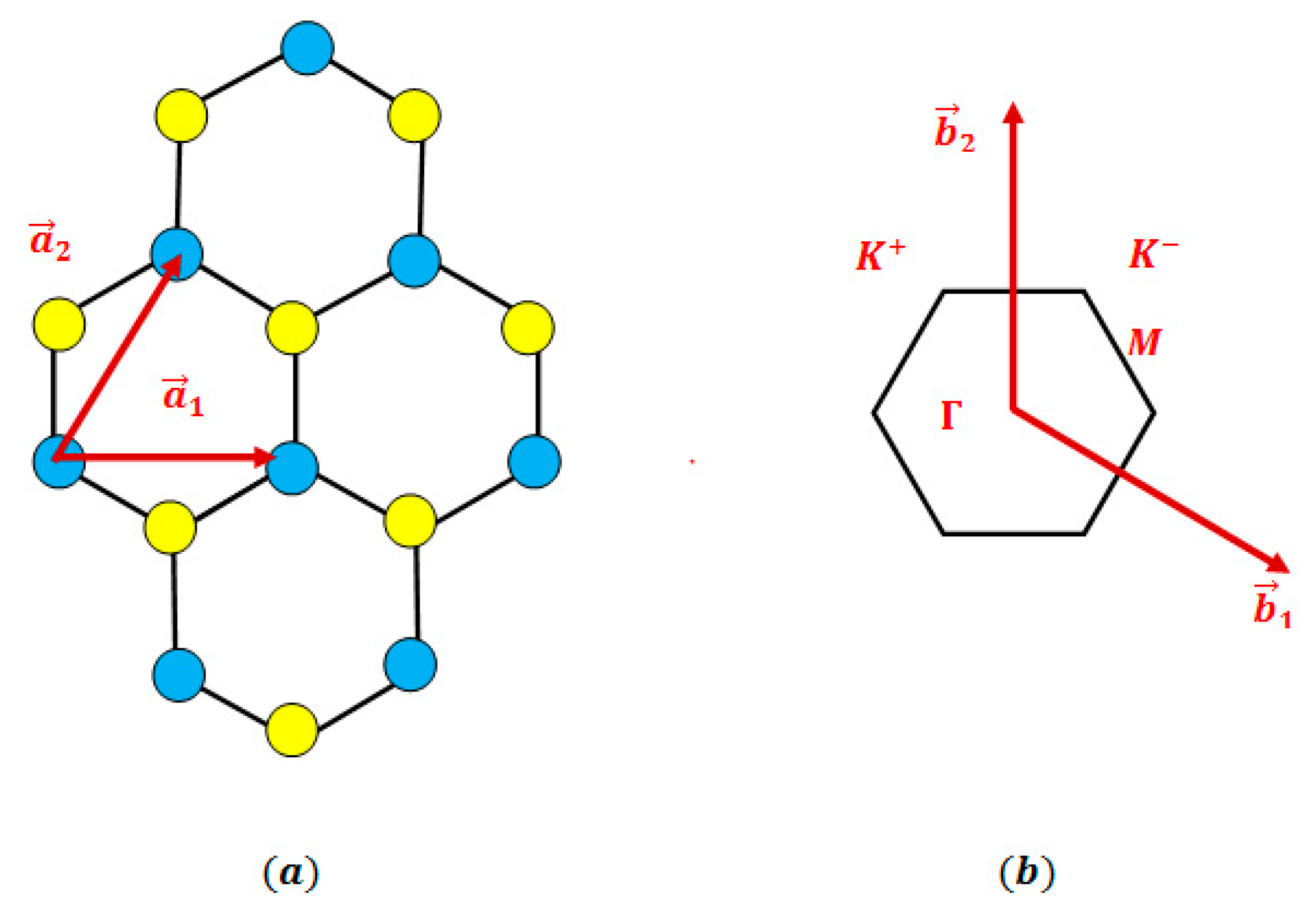
A monolayer transition metal dichalcogenide (TMDC) consists of a central layer of metal M atoms arranged in a triangular lattice, flanked by two layers of chalcogen X atoms positioned on the same triangular lattice. The triangular Bravais lattice is defined by the following basis vectors:
and (see Figure 1a).
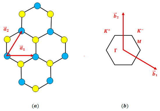
Figure 1.
(a) The triangular Bravais lattice of monolayer transition metal dichalcogenides MX2. Blue and yellow full circles denote the metal (M) and chalcogenide (X) atoms, respectively. (b) The first Brillouin zone and high-symmetry points , , and of the TMDCs in the reciprocal space of the triangular lattice. Its primitive lattice vectors are and .
Figure 1b illustrates the reciprocal lattice, defined in relation to the triangular Bravais lattice and characterized by the following vectors:
and , where is the lattice constant.
The two-dimensional Brillouin zone of the TMDCs exhibits a hexagonal shape, featuring high-symmetry points denoted as each defined as follows:
The effective 2 × 2 Hamiltonian characterizing the states of the conduction and valence bands with the parallel spins in the vicinity of the point is represented by the following expression [25,26,27]:
where denotes the two-dimensional wave vector of the electrons measured from the point ; the parameter is directly proportional to the interband matrix element of the momentum operator , where is the electron effective mass; and represents the width of the band gap.
The Hamiltonian describing a pair of spin sub-levels with in the same valley has the form of Equation (1) through the substitution , where represents the sum of the spin–orbit splitting of the conduction and valence bands. The effective Hamiltonian in the valley is derived from Equation (1) through the substitution .
The energy spectrum of the electrons derived from the Hamiltonian in Equation (1) has the following Dirac form:
Here, and correspond to the conduction and valence bands, respectively.
In our study, we use the assumption of homogeneous and defect-free interfaces between transition metal dichalcogenide monolayers and dielectric substrates as a simplification often used in theoretical models and simulations to make the problem tractable.
In this work we have investigated the electron–surface optical phonon (SOP) interaction in ML TMDCs on and dielectric substrates across long-range Fröhlich coupling. Indeed, the long-range Fröhlich coupling model provides a robust framework for understanding electron–SOP interactions in TMDCs on polar substrates. However, it relies on several approximations, for example the Born–Oppenheimer Approximation [28]. Short-range interactions [29] (e.g., electron–phonon interactions in non-polar materials) are not considered. A constant effective mass for the electron is assumed, whereas non-linear interactions and multi-phonon processes are typically neglected [30]. Impurities, defects, and other forms of disorder that can affect the electron–phonon interaction in real materials are usually not included in the idealized Fröhlich model [28,31]. Phonon dispersion is typically assumed to be linear, which is an approximation that might not hold for all phonon modes or substrates [32]. Often, a single dominant phonon mode is considered, neglecting the possible contribution of multiple phonon modes [29].
To simplify our analysis, we consider the phonon spectrum as isotropic, implying that phonons exhibit either longitudinal or transverse polarization. The Fröhlich Hamiltonian introduces an interaction term wherein an electron scatters from to , involving the emission or absorption of a phonon. In both cases, the total momentum is conserved and is expressed as follows:
The term denotes the phonon energies, incorporating both the longitudinal optical (LO) and surface optical (SO) modes, and can be expressed as follows:
In this context, and represent the creation and annihilation operators, respectively, for the phonon characterized by the wave vector , while refers to the frequency of the phonon.
The second term is the Hamiltonian of the interaction between the electron and phonon [33]:
The Fröhlich Hamiltonian is given as follows:
The interaction between carriers in monolayer transition metal dichalcogenides (TMDCs) and surface optical phonons is described by the second term in Equation (6).
The coupling element in the Fröhlich Hamiltonian represents the interaction between the electron in TMDCs and the surface optical phonon of the polar substrates. This matrix element is expressed as follows [34,35,36]:
In the given context, represents the magnitude of the polarization field, which is determined by the Fröhlich coupling [37]:
where and are the low- and high-frequency dielectric constants of the polar substrate (refer to Table 1), and represents the internal distance between the TMDCs and the polar substrate (refer to Table 2). The term denotes the energy of the SO phonons of the polar substrates with two branches,

Table 1.
The parameters for the surface polar phonon scattering of ML TMDCs on the and h polar substrates.

Table 2.
The band gap, effective electron mass and internal distance between the TMDCs and polar substrates.
The SOP energies are extracted from the bulk longitudinal optical (LO) phonons as follows [38]:
The screening of the Coulomb interaction by the polar dielectric environment is considered through . Given the weak screening of the electric field perpendicular to the plane of the ML TMDCs, is set to 1 [44].
On polar substrates, surface optical phonons (SOPs) induce an electric field that interacts with the electrons in the neighboring ML TMDCs. Using Equations (7) and (8), the SOP coupling is expressed as
The summation is performed over one spin and one valley, where is the area of the two-atom unit cell.
In our analysis in the present case, we have followed the same theoretical method presented in our previous calculations [14,15,16]. So, to study the interactions between electrons and surface optical phonons in ML TMDCs, we have specifically considered the electronic states and , with electron energies and , respectively. We have also considered the effective 2 × 2 Hamiltonian characterizing the states of the conduction and valence bands with the parallel spins in the vicinity of the point of the hexagonal Brillouin zone.
The space of polaronic states results from a tensor product between the two subspaces of electronic and phononic states. Thus, we consider new states called polaronic states given by
The polaron electron energies for the states in ML TMDCs on polar substrates are given below [14,15,16]:
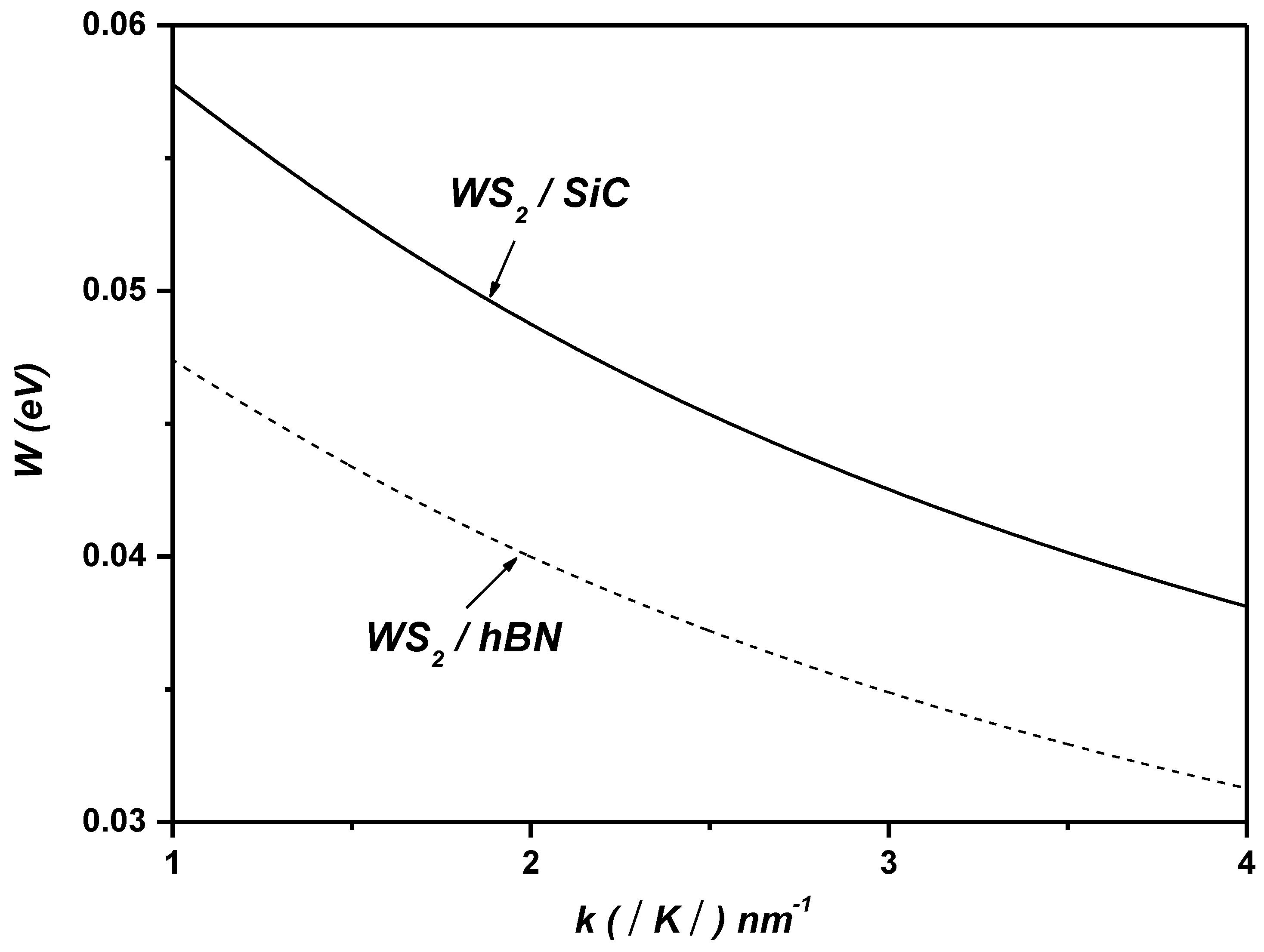
Figure 2 depicts the SO coupling strength between the electronic states and versus the wave vector in ML WS2 on the and h polar substrates. As shown in Figure 2, it is evident that the coupling with SOPs is significantly influenced by the type of polar substrate.

Figure 2.
The SO coupling strength between the electronic states and versus the wave vector in ML WS2 on and h polar substrates.
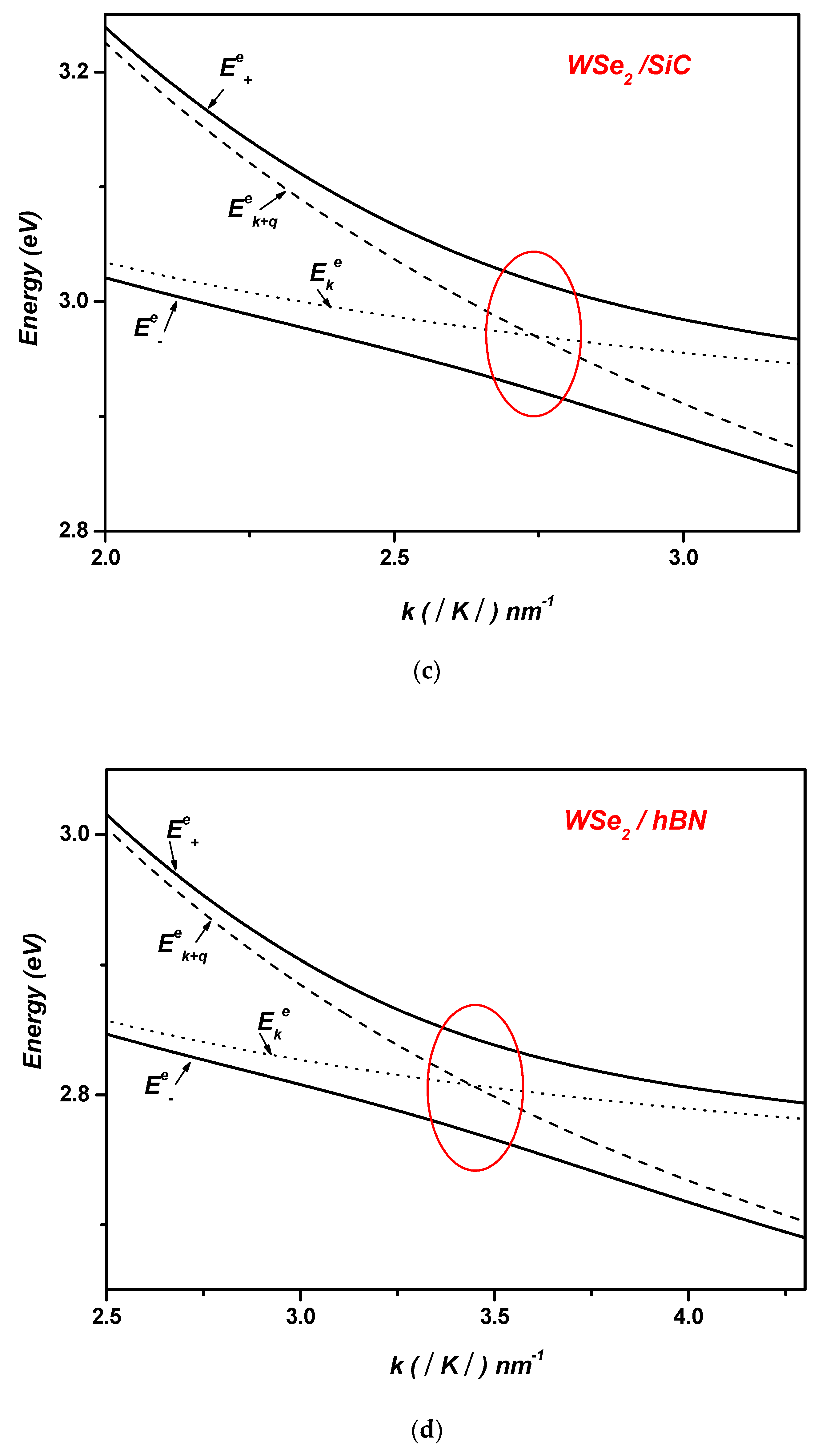
We show in Figure 3 the polaron electron energies versus the wave vector in ML on and h polar substrates. For comparison purposes, we have included in the same figure the energies of the noninteracting states and . For example, in the case of WS2, these noninteracting levels cross near in the case of and near in the case of indicating resonant coupling (see Table 3). These crossings indicate that the separation between electronic levels is equal to in both the and cases, where respectively. In fact, the electronic level crossings are clearly replaced by significant anticrossings, with energy levels approximately at ~94 meV and ~70 meV for and polar substrates, respectively. In Figure 3, the enhancement of the Rabi splitting of the electron levels when shifting from to can be also observed (refer to Table 4, Figure 3).
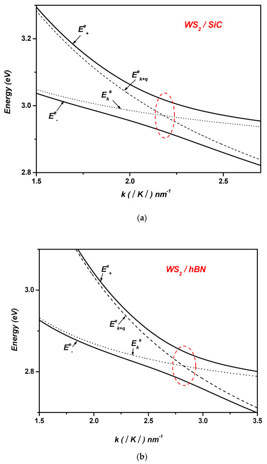
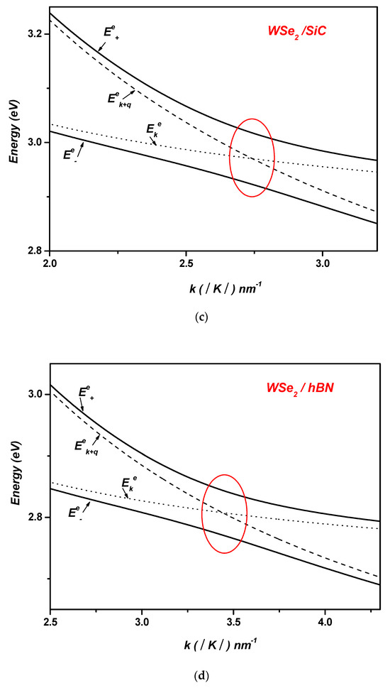
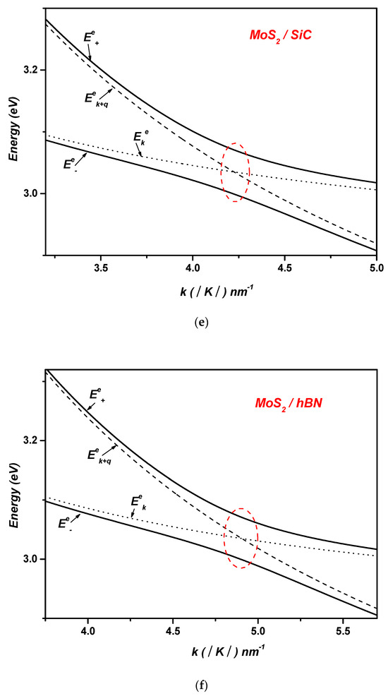
Figure 3.
Polaron electron energies as a function of the wave vector in the following ML TMDCs on SiC and hBN polar substrates, respectively: (a) and (b) WS2; (c) and (d) WSe2; (e) and (f) MoS2.

Table 3.
The crossing values of the noninteracting states in the ML for both the and polar substrates.

Table 4.
The Rabi splitting of the electron levels in the ML for both the and polar substrates.
In polar substrates, surface optical (SO) phonons generate an electric field that extends into the overlying monolayer. This electric field directly couples with the electrons in the TMDC layer through dipole interactions, resulting in a significant enhancement of the coupling strength. This interaction manifests as a renormalization of the electronic levels, which increases the energy splitting between the hybridized states and enhances the Rabi splitting.
The difference in Rabi splitting between SiC and hBN as polar substrates for a TMDC monolayer (see Table 4 and Figure 3) can be attributed to the distinct surface phonon properties, dielectric characteristics, and phonon energy scales of each material. SiC, for instance, has a higher dielectric constant than hBN. A higher dielectric constant typically results in stronger electric fields generated by surface phonons near the interface, thereby enhancing the coupling with the electronic states of the TMDC. This intensification of the electron–phonon interaction can lead to larger Rabi splitting.
Conversely, hBN, with its lower dielectric constant, produces relatively weaker electric fields associated with its surface phonons. Consequently, the electron–phonon coupling with the TMDC monolayer is slightly weaker, resulting in smaller Rabi splitting. This comparison underscores the critical role that the choice of polar substrate plays in determining the optical properties and performance of TMDC-based devices.
In these anticrossings, the wave functions of the levels become mixed, allowing for multiple transitions, such as , , and . This demonstrates that the interaction between electrons and surface polar phonons cannot be considered a weak coupling. The coupling between electrons and SOPs leads to the Rabi splitting of the electronic levels. Hence, the calculations indicate the possibility of an energetically resonant coupling between the electronic sub-levels and the surface vibration modes in ML TMDCs on the studied polar substrates. Furthermore, the two resulting polaron states can be expressed as follows:
The weight of the electronic component and the weight of the one-phonon component of the polaron states ± vary with the polaron energies . The expressions detailing these dependencies are as follows [14,15,16]:
where is the SO coupling strength between the electronic states [14,15,16,17].
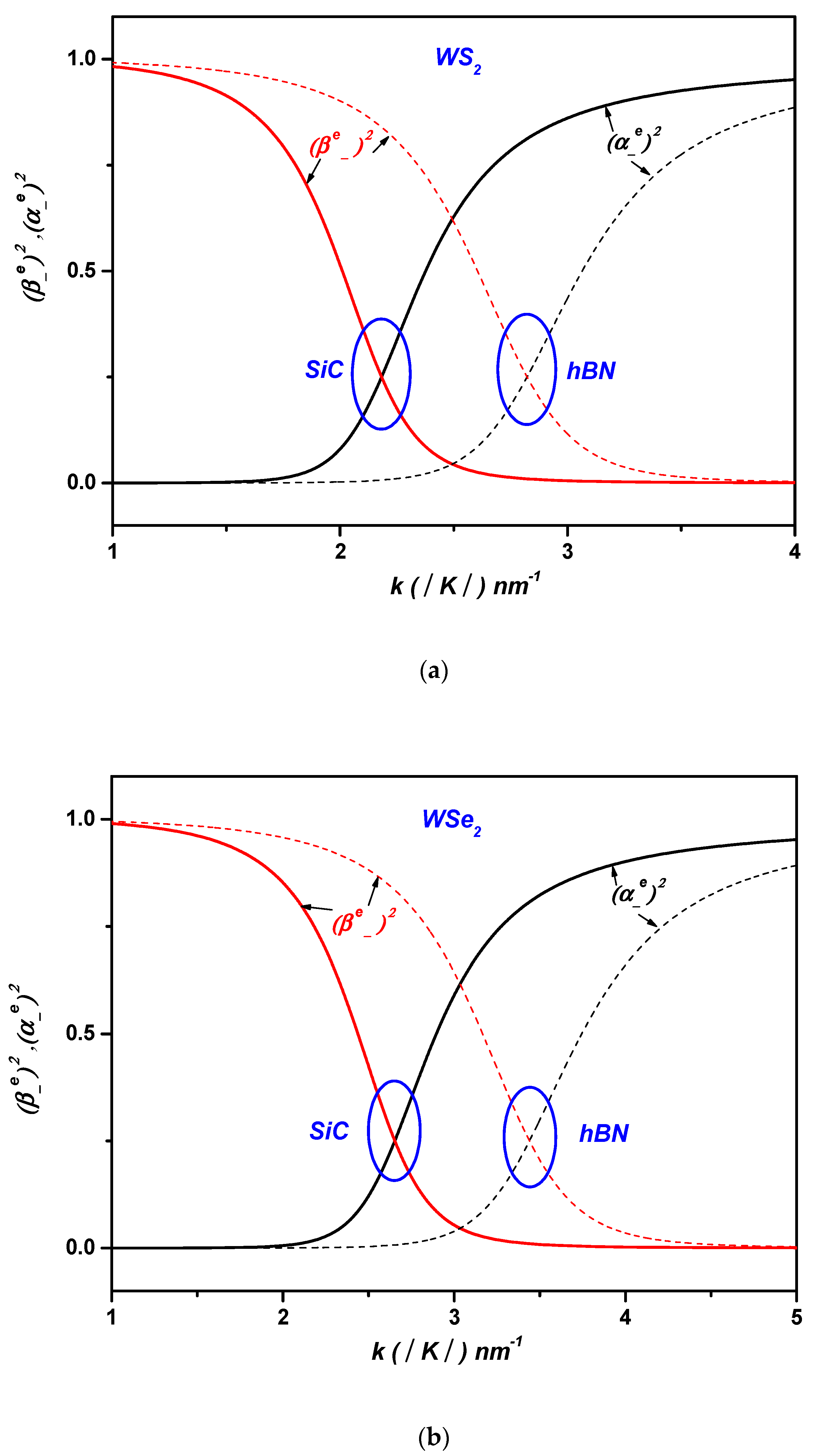
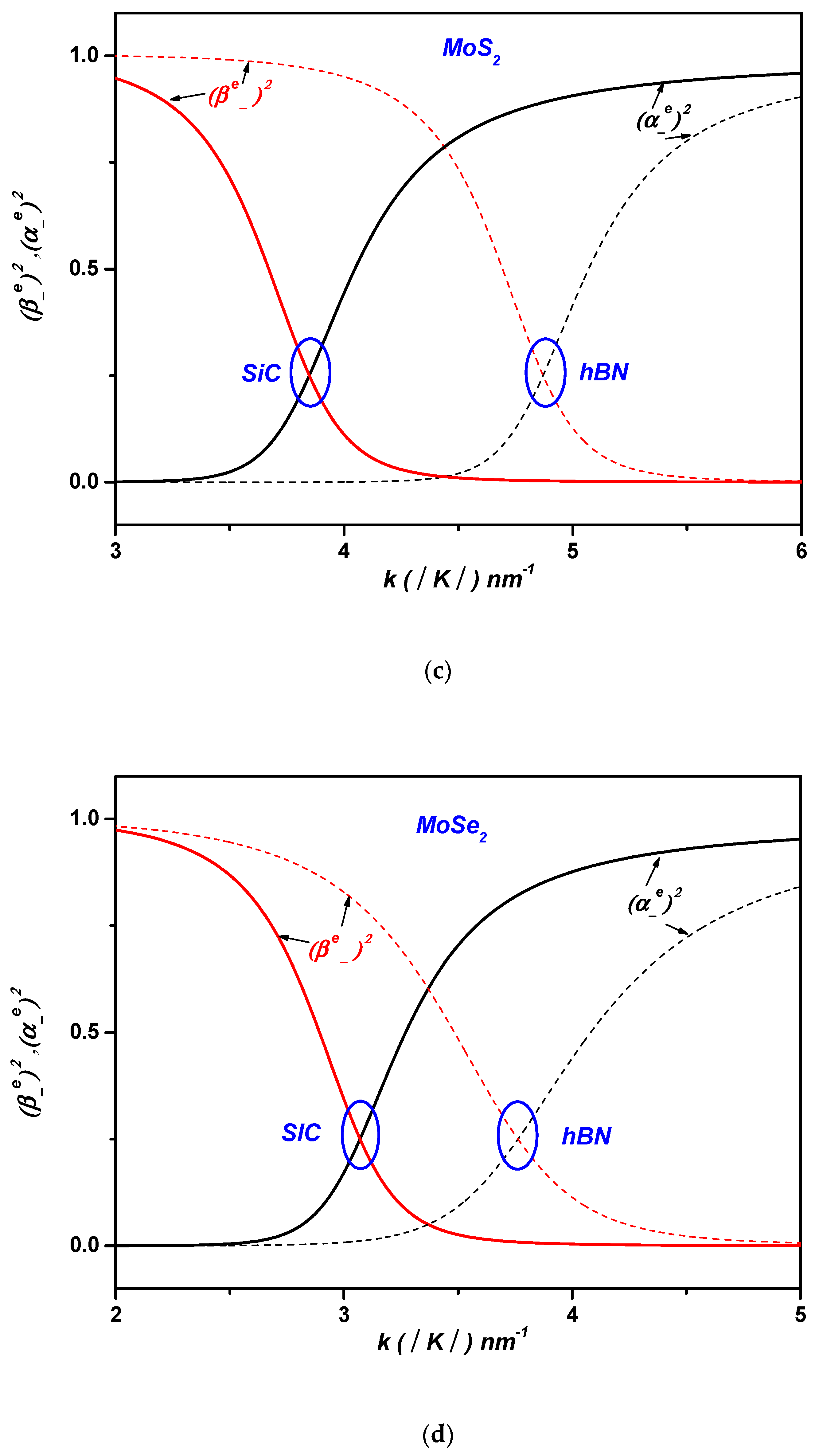
Figure 4 depicts the weight of the electronic components and the one-phonon components of the lower polaron state in ML TMDCs for and h polar substrates as a function of the wave vector in ML TMDCs. It can be seen, for example, in the case of on the polar substrate (see Table 3, Figure 4) that when the wave vector approaches the value of the weight of the one-phonon component for the lower polaron state is much larger compared with that of the electronic component . This result demonstrates that the SOP situated at the interface of the ML on the polar substrate plays a crucial role in the resonant coupling between the noninteracting states and , allowing for the formation of the polaron states. It can be noted that the same result has been proved for the other cases of ML on the and h polar substrates (see Table 3 and Figure 4).

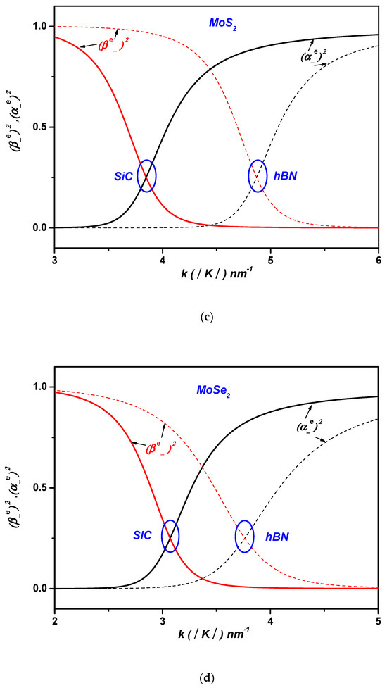
Figure 4.
The weight of the electronic components and the one-phonon components of the lower polaron state in ML TMDCs on the and dielectric substrates (a) in , (b) in , (c) in , and (d) in versus the wave vector .
3. Polaronic Oscillator Strength of ML TMDCs on SiC and hBN Polar Substrates
In the following section, we theoretically investigate the polaronic oscillator strength (OS), which is another crucial quantity. Drawing an analogy with the oscillator strengths of interband transitions in quantum dots, we have computed the OS for the interband transitions in ML TMDCs on polar substrates. In the strong confinement limit, the OS is linked to the overlap integral of the polaronic states, , by the following equation [45,46]:
where is the Kane energy and is the emission energy for one phonon of the ML TMDCs on the polar substrates, which is given by
where is the lower polaron energy of the exciton, is the emitted photon energy, and is the energy gap of the ML TMDCs.
We have calculated the OS for the lower polaron state , which is a linear combination of the two states and :
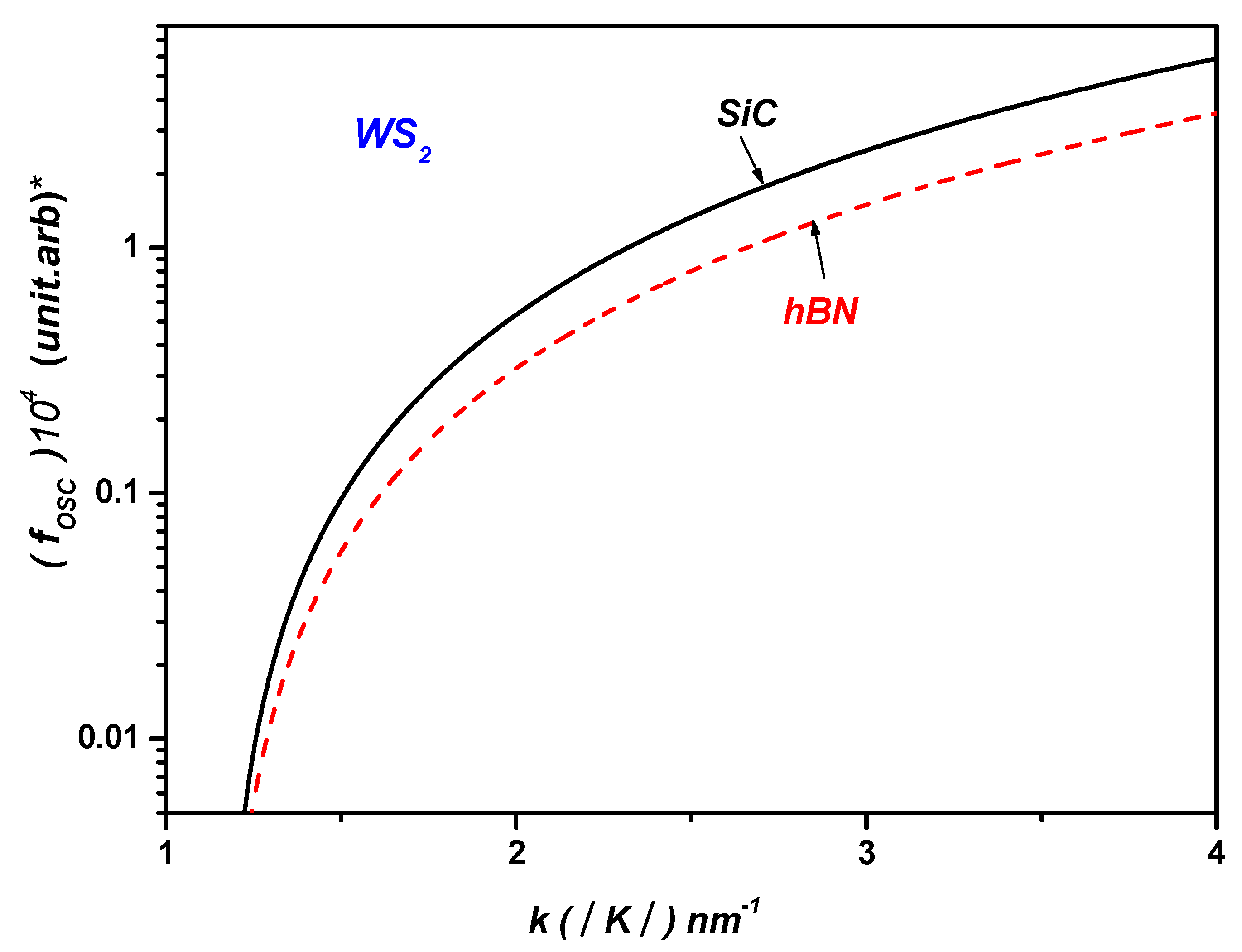
Figure 5 shows the polaronic OS of on the and h polar substrates versus the wave vector in ML .
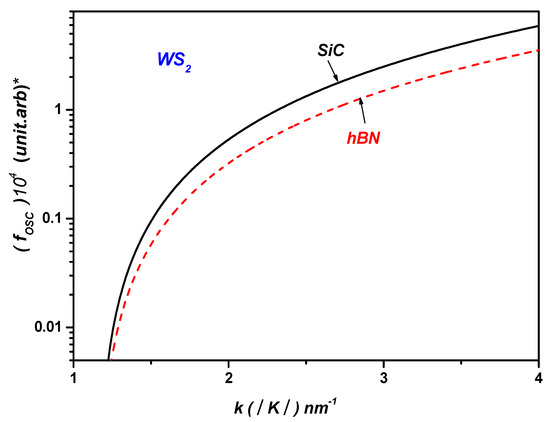
Figure 5.
The polaronic OS of on the and h polar substrates versus the wave vector in the ML . (*) in y-axis is multiplication sign.
As a result, we have theoretically proven that the polaronic OS is especially sensitive to the phonon mode of the surrounding dielectrics. In fact, this result is due to the emission energy for one phonon of the ML TMDCs for the and h polar substrates, which is given by . Hence, the highest polaronic oscillator strength corresponds to the highest optical phonon energy of the polar substrates, . This is analogous to the polaronic oscillator strength in ML TMDCs, which is also much higher compared with conventional semiconductors [6,7,8,9].
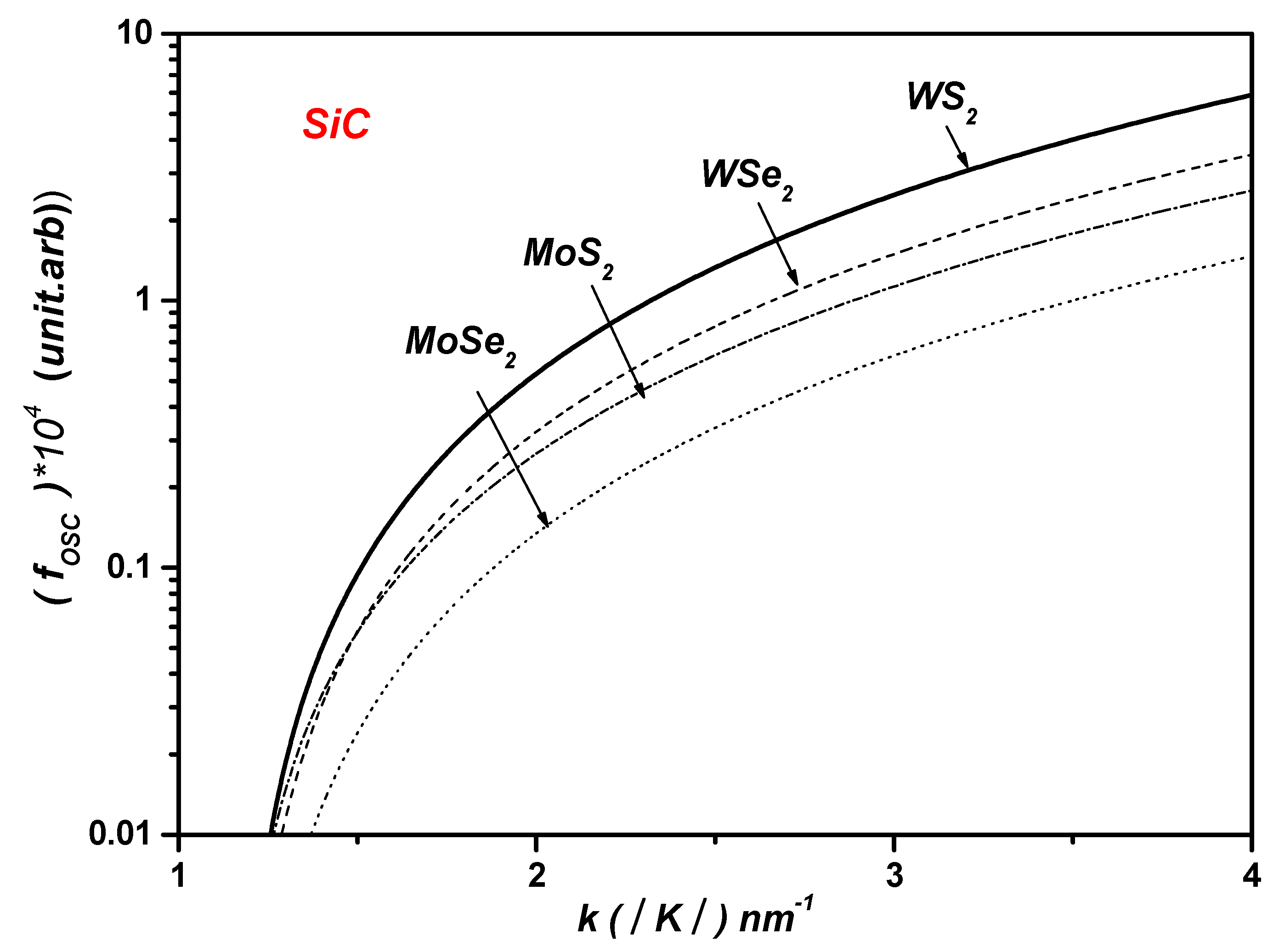
Using the same method, we can easily prove that for the other ML TMDCs such as , , and ,
This result is due to the dielectric constant, as well as the phonon energy, compared with that of (see Table 1), so the polarization field created near the interface should be the highest in the case of the substrate compared with the substrate. This result leads to the highest polaronic OS in ML TMDCs on the polar substrate. Similarly, it can be concluded from Figure 6 that
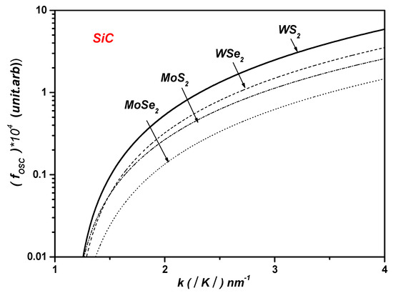
Figure 6.
The polaronic OS in the MLs on the polar substrate versus the wave vector . (*) in y-axis is multiplication sign.
Hence, this result can be explained by the difference in the electron effective masses in ML TMDCs. This result actually confirms the decrement in the polaronic OS for heavy electrons in the nearby ML TMDC/dielectric substrate interface. Otherwise, in the case of light electrons, the polaronic OS increases considerably in the strong confinement regime.
4. Polaronic Scattering Rate of ML TMDCs on SiC and hBN Polar Substrates
Now, we consider the temperature dependence of the polaronic scattering rate due to the SO phonons. The polaronic scattering rate (SO phonon scattering rate) is given as follows [17]:
Here, is the Bose–Einstein phonon occupation number, is a directional angle of the wave vector , and is given by
The summation ∑ is replaced by the integral (the sum over a spin and a valley), where is the area of the elementary cell that contains two atoms.
Thus,
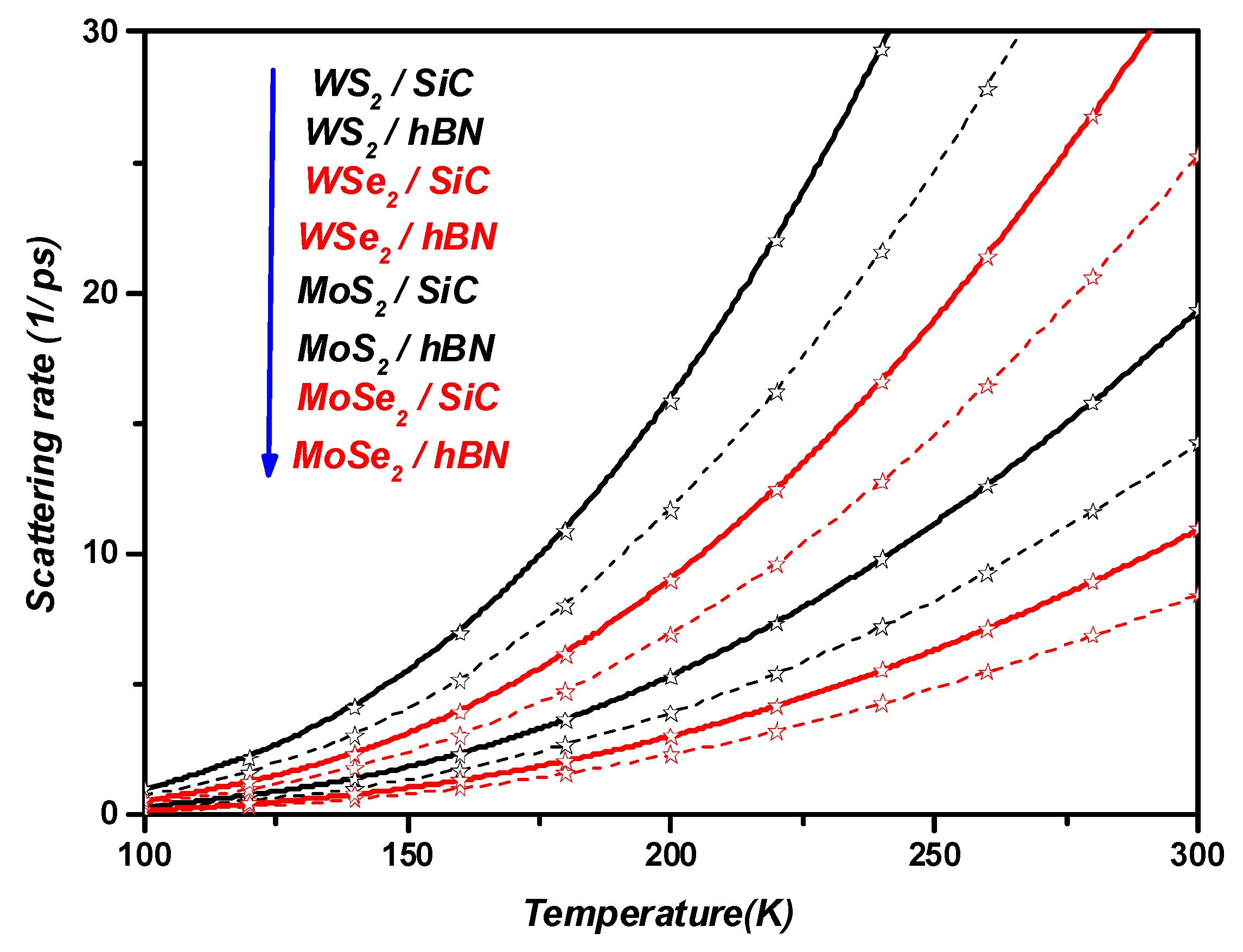
Figure 7 shows the temperature dependence of the SO phonon scattering rate in ML TMDCs on the and h polar substrates. We clearly see that at temperatures higher than room temperature, the SO phonon scattering rate increases with temperature, whereas at low temperatures, the SO phonon scattering rate is not significant. Similarly, it can be concluded from Figure 7 that
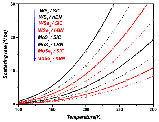
Figure 7.
The temperature dependence of the SO phonon scattering rate in the MLs on the and h polar substrates. Stars represent the calculated points on the graph.
From Figure 7, we can also observe that the SO phonon scattering rate in ML TMDCs depends strongly on the dielectric constant of the polar substrate, as follows:
Finally, by choosing a suitable dielectric as a substrate, one can achieve the highest SO phonon scattering rate in ML TMDCs.
To experimentally test the electron–surface optical phonon (SOP) interaction in transition metal dichalcogenides (TMDCs) deposited on silicon carbide or hexagonal boron nitride dielectric substrates, we propose several experiments, such as Photoluminescence (PL) Spectroscopy, Raman spectroscopy, Time-Resolved Photoluminescence (TRPL), Electroluminescence (EL) Spectroscopy, and Angle-Resolved Photoemission Spectroscopy (ARPES) [22,47,48,49,50].
Our theoretical findings reveal that the coupling between surface optical phonons (SOP) and monolayer TMDCs is significantly influenced by the choice of polar substrate and has promising implications for advancing 2D material-based optoelectronic devices. This coupling between electronic sub-levels in TMDCs and surface polar vibration modes on polar substrates not only leads to Rabi splitting but also strengthens electronic interactions with surface phonons. These enhanced interactions open several pathways for optimizing device performance across various applications.
A key insight is that strong resonant coupling between TMDC electrons and surface optical phonons can reduce nonradiative recombination by channeling energy into radiative decay pathways. This boost in photoluminescence efficiency is especially valuable for light-emitting devices, such as LEDs, where maximizing photon emission is crucial. By selecting substrates that induce greater Rabi splitting, such as SiC or hBN, designers can achieve brighter, more efficient emitters.
Furthermore, our findings show that stronger polarization fields at the TMDC–substrate interface lead to increased polaronic optical strength and higher scattering rates. This polarization effect, which can be adjusted by selecting specific polar substrates, has significant implications for carrier mobility. For example, high-dielectric substrates like SiC can enhance mobility by modulating electron–phonon interactions, a result corroborated by Sanjay Gopalan et al. [24]. These insights can inform the selection of substrate materials for engineering high-mobility TMDC transistors, essential for low-power, high-speed electronic devices.
Additionally, coupling in SOP modes creates polaronic states that influence energy relaxation dynamics in TMDCs. By tuning the SOP interaction strength through substrate choice, we can control the rate and pathways of phonon-assisted hot carrier relaxation, which is relevant for applications like photovoltaics and photodetectors. The ability to manage energy dissipation could result in devices with improved efficiency and faster response times.
Our study also highlights that the resonant coupling between TMDC electrons and surface phonons can enhance Raman scattering processes. This enhancement aligns with the experimental findings by Colin M. Chow et al. [22] and can be leveraged in devices that require precise optical control, such as tunable filters, sensors, or Raman spectroscopy applications, as previously demonstrated by Bastian Miller et al. [23].
Overall, these potential applications demonstrate that a deep understanding of substrate-dependent SOP coupling provides a strong foundation for tailoring and improving the optical and electronic properties of monolayer TMDC-based devices. This foundational insight into SOP coupling can guide both material and substrate selection for specific functionalities across various optoelectronic applications.
5. Conclusions
In conclusion, our results indicate that the SOP coupling in ML TMDCs depends strongly upon the polar substrate. Moreover, the resonant coupling between electronic sub-levels and surface polar vibration modes leads to the Rabi splitting of electron levels in single-layer TMDCs. Hence, the polarization field induces robust resonant mixing between electronic states and surface vibration modes when their energies become comparable. This resonant coupling has the potential to diminish the probability of nonradiative recombination processes and enhance the efficiency of photoluminescence (PL). Finally, we demonstrate that the highest polarization field created near the interface leads to the highest polaronic OS and the enhancement of SO phonon scattering rates in ML TMDCs. Thus, polaronic OS and polaronic scattering rates depend strongly upon the choice of the polar substrate. The presence of polaronic states may yield significant implications for energy relaxation in ML TMDCs. Moreover, the interaction between electrons and surface optical phonons is a crucial factor influencing the physical characteristics of 2D semiconductors, particularly influencing processes like phonon-assisted hot carrier relaxation.
Author Contributions
Conceptualization and visualization M.M., R.B. and S.G.; methodology, M.M.; investigation and formal analysis, M.M.; writing—original draft preparation, M.M.; writing—review and editing, M.M., R.B. and S.G.; supervision, S.G. All authors have read and agreed to the published version of the manuscript.
Funding
This research received no external funding.
Institutional Review Board Statement
Not applicable.
Informed Consent Statement
Not applicable.
Data Availability Statement
The data presented in this study are available on request from the corresponding author. The data are not publicly available due to privacy issues.
Conflicts of Interest
The authors declare no conflicts of interest.
References
- Wang, Z.; Nie, Y.; Ou, H.; Chen, D.; Cen, Y.; Liu, J.; Wu, D.; Hong, G.; Li, B.; Xing, G.; et al. Electronic and Optoelectronic Monolayer WSe2 Devices via Transfer-Free Fabrication Method. Nanomaterials 2023, 13, 1368. [Google Scholar] [CrossRef] [PubMed]
- Ahmed, T.; Zha, J.; Lin, K.K.H.; Kuo, H.-C.; Tan, C.; Lin, D.H. Bright and Efficient Light-Emitting Devices Based on 2D Transition Metal Dichalcogenides. Adv. Mater. 2023, 35, 2208054. [Google Scholar] [CrossRef] [PubMed]
- Joseph, S.; Mohan, J.; Lakshmy, S.; Thomas, S.; Chakraborty, B.; Thomas, S.; Kalarikkal, N. A review of the synthesis, properties, and applications of 2D transition metal dichalcogenides and their heterostructures. Mater. Chem. Phys. 2023, 297, 127332. [Google Scholar] [CrossRef]
- Lau, C.S.; Chee, J.Y.; Cao, L.; Ooi, Z.-E.; Tong, S.W.; Bosman, M.; Bussolotti, F.; Deng, T.; Wu, G.; Yang, S.-W.; et al. Gate-Defined Quantum Confinement in CVD 2D WS2. Adv. Mater. 2022, 34, 2103907. [Google Scholar] [CrossRef]
- Zhang, L.; Ni, R.; Zhou, Y. Controlling quantum phases of electrons and excitons in moiré superlattices. J. Appl. Phys. 2023, 133, 080901. [Google Scholar] [CrossRef]
- Ardizzone, V.; De Marco, L.; De Giorgi, M.; Dominici, L.; Ballarini, D.; Sanvitto, D. Emerging 2D materials for room-temperature polaritonics. Nanophotonics 2019, 8, 1547–1558. [Google Scholar] [CrossRef]
- Xie, K.; Li, X.; Cao, T. Theory and Ab Initio Calculation of Optically Excited States—Recent Advances in 2D Materials. Adv. Mater. 2021, 33, 1904306. [Google Scholar] [CrossRef]
- Palummo, M.; Bernardi, M.; Grossman, J.C. Exciton Radiative Lifetimes in Two-Dimensional Transition Metal Dichalcogenides. Nano Lett. 2015, 15, 2794–2800. [Google Scholar] [CrossRef]
- Qiu, D.Y.; Cao, T.; Steven, G. Louie, Nonanalyticity, Valley Quantum Phases, and Lightlike Exciton Dispersion in Monolayer Transition Metal Dichalcogenides: Theory and First-Principles Calculations. Phys. Rev. Lett. 2015, 115, 176801. [Google Scholar] [CrossRef]
- Huang, C.-C.; Wang, H.; Cao, Y.; Weatherby, E.; Richheimer, F.; Wood, S.; Jiang, S.; Wei, D.; Dong, Y.; Lu, X.; et al. Facilitating Uniform Large-Scale MoS2, WS2 Monolayers, and Their Heterostructures through van der Waals Epitaxy. ACS Appl. Mater. Interfaces 2022, 14, 42365–42373. [Google Scholar] [CrossRef]
- Wada, N.; Pu, J.; Takaguchi, Y.; Zhang, W.; Liu, Z.; Endo, T.; Irisawa, T.; Matsuda, K.; Miyauchi, Y.; Takenobu, T.; et al. Efficient and Chiral Electroluminescence from In-Plane Heterostructure of Transition Metal Dichalcogenide Monolayers. Adv. Funct. Mater. 2022, 32, 2203602. [Google Scholar] [CrossRef]
- Robert, C.; Han, B.; Kapuscinski, P.; Delhomme, A.; Faugeras, C.; Amand, T.; Molas, M.R.; Bartos, M.; Watanabe, K.; Taniguchi, T.; et al. Measurement of the spin-forbidden dark excitons in MoS2 and MoSe2 monolayers. Nat. Commun. 2020, 11, 4037. [Google Scholar] [CrossRef] [PubMed]
- Carrascoso, F.; Li, H.; Frisenda, R.; Castellanos-Gomez, A. Strain engineering in single-, bi- and tri-layer MoS2, MoSe2, WS2 and WSe2. Nano Res. 2021, 14, 1698–1703. [Google Scholar] [CrossRef]
- Mahdouani, M. Investigation of the electron-surface phonon interaction effects in graphene on a substrate made of polar materials. PHYSE 2017, 87, 192–198. [Google Scholar] [CrossRef]
- Mahdouani, M.; Gardelis, S.; Bourguiga, R. The effect of Si impurities on the transport properties and the electron-surface phonon interaction in single layer graphene deposited on polar substrates. Phys. B Condens. Matter 2018, 550, 171–178. [Google Scholar] [CrossRef]
- Mahdouani, M.; Bourguiga, R. Auger and carrier-surface phonon interaction processes in graphene on a substrate made of polar materials. Superlattices Microstruct. 2017, 102, 212–220. [Google Scholar] [CrossRef]
- Perebeinos, V.; Avouris, P. Inelastic scattering and current saturation in graphene. Phys. Rev. B 2010, 81, 195442. [Google Scholar] [CrossRef]
- Mahdouani, M.; Bourguiga, R.; Jaziri, S. Polaronic states in Si nanocrystals embedded in SiO2 matrix. Physica E 2008, 41, 228–234. [Google Scholar] [CrossRef]
- Mahdouani, M.; Gardelis, S.; Nassiopoulou, A.G. Role of surface vibration modes in Si nanocrystals within light emitting porous Si at the strong confinement regime. J. Appl. Phys. 2011, 110, 023527. [Google Scholar] [CrossRef]
- Gardelis, S.; Nassiopoulou, A.G.; Mahdouani, M.; Bourguiga, R.; Jaziri, S. Enhancement and red shift of photoluminescence (PL) of fresh porous Si under prolonged laser irradiation or ageing: Role of surface vibration modes. Physica E 2009, 41, 986–989. [Google Scholar] [CrossRef]
- Paul, S.; Karak, S.; Talukdar, S.; Negi, D.; Saha, S. Influence of Edges and Interlayer Electron–phonon Coupling in WS2/h-BN Heterostructure. ACS Appl. Mater. Interfaces 2024, 16, 40077–40085. [Google Scholar] [CrossRef] [PubMed]
- Chow, C.M.; Yu, H.; Jones, A.M.; Yan, J.; Mandrus, D.G.; Taniguchi, T.; Watanabe, K.; Yao, W.; Xu, X. Unusual Exciton–Phonon Interactions at van der Waals Engineered Interfaces. Nano Lett. 2017, 17, 1194–1199. [Google Scholar] [CrossRef] [PubMed]
- Miller, B.; Lindlau, J.; Bommert, M.; Neumann, A.; Yamaguchi, H.; Högele, A. Tuning the Fröhlich exciton-phonon scattering in monolayer MoS. Nat. Commun. 2019, 10, 807. [Google Scholar] [CrossRef] [PubMed]
- Gopalan, S.; Van de Put, M.L.; Gaddemane, G.; Fischetti, M.V. Theoretical Study of Electronic Transport in Two-Dimensional Transition Metal Dichalcogenides: Effects of the Dielectric Environment. Phys. Rev. Appl. 2022, 18, 054062. [Google Scholar] [CrossRef]
- Glazov, M.M.; Ivchenko, E.L. Valley Orientation of Electrons and Excitons in Atomically Thin Transition Metal Dichalcogenide Monolayers. JETP Lett. 2021, 113, 7–17. [Google Scholar] [CrossRef]
- Durnev, M.V.; Glazov, M.M. Excitons and trions in two-dimensional semiconductors based on transition metal dichalcogenides. Phys.–Uspekhi 2018, 61, 825–845. [Google Scholar] [CrossRef]
- Kormanyos, A.; Burkard, G.; Gmitra, M.; Fabian, J.; Zolyomi, V.; Drummond, N.D.; Fal’ko, V. k·p theory for two-dimensional transition metal dichalcogenide semiconductors. 2D Mater. 2015, 2, 022001. [Google Scholar] [CrossRef]
- Antonius, G.; Louie, S.G. Theory of exciton-phonon coupling. Phys. Rev. B 2022, 105, 085111. [Google Scholar] [CrossRef]
- Sohier, T.; Calandra, M.; Mauri, F. Two-dimensional Fröhlich interaction in transition-metal dichalcogenide monolayers: Theoretical modeling and first-principles calculations. Phys. Rev. B 2016, 94, 085415. [Google Scholar] [CrossRef]
- Wang, Y.; He, C.; Tan, Q.; Tang, Z.; Huang, L.; Liu, L.; Yin, J.; Wang, X.; Pan, A. Exciton–phonon coupling in two-dimensional layered (BA)2PbI4 perovskite microplates. RSC Adv. 2023, 13, 5893–5899. [Google Scholar] [CrossRef]
- Ma, J.; Xu, D.; Hu, R.; Luodoi, X. Examining two-dimensional Fröhlich model and enhancing the electron mobility of monolayer InSe by dielectric engineering. J. Appl. Phys. 2020, 128, 035107. [Google Scholar] [CrossRef]
- Hinsche, N.F.; Thygesen, K.S. Electron–phonon interaction and transport properties of metallic bulk and monolayer transition metal dichalcogenide TaS2. 2D Mater. 2017, 5, 015009. [Google Scholar] [CrossRef]
- Xiao, Y.; Li, Z.Q.; Wang, Z.W. Polaron effect on the bandgap modulation in monolayer transition metal dichalcogenides. J. Phys. Cond. Matter 2017, 29, 485001. [Google Scholar] [CrossRef] [PubMed]
- Nguepnang, J.V.; Kenfack, C.; Kenfack, A.; Fobasso, M.F.C.; Sun, Y. Optical signature of bipolaron in monolayer transition metal dichalcogenides: All coupling approach. Opt. Quantum Electron. 2021, 53, 728. [Google Scholar] [CrossRef]
- Devreese, J.T.; Huybrechts, W.; Lemmeks, L. On the optical absorption of free polarons at weak coupling. Phys. Status Solidi 1971, 48, 77–86. [Google Scholar] [CrossRef]
- Mafra, D.L.; Araujo, P.T. Intra- and Interlayer Electron-Phonon Interactions in 12/12C and 12/13C BiLayer Graphene. Appl. Sci. 2014, 4, 207–239. [Google Scholar] [CrossRef]
- Wang, S.Q.; Mahan, G.D. Electron Scattering from Surface Excitations. Phys. Rev. B 1972, 6, 4517. [Google Scholar] [CrossRef]
- Schiefele, J.; Sols, F.; Guinea, F. Temperature dependence of the conductivity of graphene on boron nitride. Phys. Rev. B 2012, 85, 195420. [Google Scholar] [CrossRef]
- Geick, R.; Perry, C.H.; Rupprecht, G. Normal Modes in Hexagonal Boron Nitride. Phys. Rev. 1966, 146, 543. [Google Scholar] [CrossRef]
- Rozhkov, A.V.; Nori, F. Exact wave functions for an electron on a graphene triangular quantum dot. Phys. Rev. B 2010, 81, 155401. [Google Scholar] [CrossRef]
- Han, B.; Robert, C.; Courtade, E.; Manca, M.; Shree, S.; Amand, T.; Renucci, P.; Taniguchi, T.; Watanabe, K.; Marie, X.; et al. Exciton States in Monolayer MoSe2 and MoTe2 Probed by Up conversion Spectroscopy. Phys. Rev. X 2018, 8, 031073. [Google Scholar] [CrossRef]
- Wang, G.; Gerber, I.C.; Bouet, L.; Lagarde, D.; Balocchi, A.; Vidal, M.; Palleau, E.; Amand, T.; Marie, X.; Urbaszek, B. Exciton states in monolayer MoSe2: Impact on interband transitions. 2D Mater. 2015, 2, 045005. [Google Scholar] [CrossRef]
- Laturia, A.; Van de Put, M.L.; Vandenberghe, W.G. Dielectric properties of hexagonal boron nitride and transition metal dichalcogenides: From monolayer to bulk. 2D Mater. Appl. 2018, 2, 6. [Google Scholar] [CrossRef]
- Benedict, L.X.; Louie, S.G.; Cohen, M.L. Static polarizabilities of single-wall carbon nanotubes. Phys. Rev. B 1995, 52, 8541. [Google Scholar] [CrossRef]
- Hwang, E.H.; Sarma, S.D. Surface polar optical phonon interaction induced many-body effects and hot-electron relaxation in graphene. Phys. Rev.B 2013, 87, 115432. [Google Scholar] [CrossRef]
- Mahdouani, M.; Zalfani, M.; Bourguiga, R.; Su, B.-L. Radiative and non radiative recombinations study in the novel nanocomposites BiVO4/3DOM-TiO2, ZnO/3DOM-TiO2 and BiVO4/3DOM-ZnO: Application to the photocatalysis. Physica E 2019, 108, 269–280. [Google Scholar] [CrossRef]
- Chang, Y.-C.; Chan, Y.-C.; Das, B.; Syue, J.-F.; Hu, H.-C.; Lan, Y.-W.; Lu, T.-H. Distinctive characteristics of exciton-phonon interactions in optically driven MoS. Phys. Rev. Mater. 2024, 8, 074003. [Google Scholar] [CrossRef]
- Nguepnang, J.V.; Kenfack-Sadem, C.; Kenfack-Jiotsa, A.; Guimapi, C.; Fotue, A.J.; Merad, A.E. Electron–phonon coupling contribution on the optical absorption and the dynamic of exciton-polaron in monolayer Transition Metal Dichalcogenides. Opt. Quantum Electron. 2021, 53, 654. [Google Scholar] [CrossRef]
- Lai, J.-M.; Xie, Y.-R.; Zhang, J. Detection of electron-phonon coupling in two-dimensional materials by light scattering. Nano Res. 2021, 14, 1711–1733. [Google Scholar] [CrossRef]
- Jiang, Y.; Chen, S.; Zheng, W.; Zheng, B.; Pan, A. Interlayer exciton formation, relaxation, and transport in TMD van der Waals heterostructures. Light Sci. Appl. 2021, 10, 72. [Google Scholar] [CrossRef]
Disclaimer/Publisher’s Note: The statements, opinions and data contained in all publications are solely those of the individual author(s) and contributor(s) and not of MDPI and/or the editor(s). MDPI and/or the editor(s) disclaim responsibility for any injury to people or property resulting from any ideas, methods, instructions or products referred to in the content. |
© 2024 by the authors. Licensee MDPI, Basel, Switzerland. This article is an open access article distributed under the terms and conditions of the Creative Commons Attribution (CC BY) license (https://creativecommons.org/licenses/by/4.0/).

