
Rietveld Refinement of Electron Diffraction Patterns of Nanocrystalline Materials Using MAUD: Two-Beam Dynamical Correction Implementation and Applications

Abstract
:1. Introduction
2. Dynamical Scattering Approximation as Implemented in MAUD
3. Materials and Methods
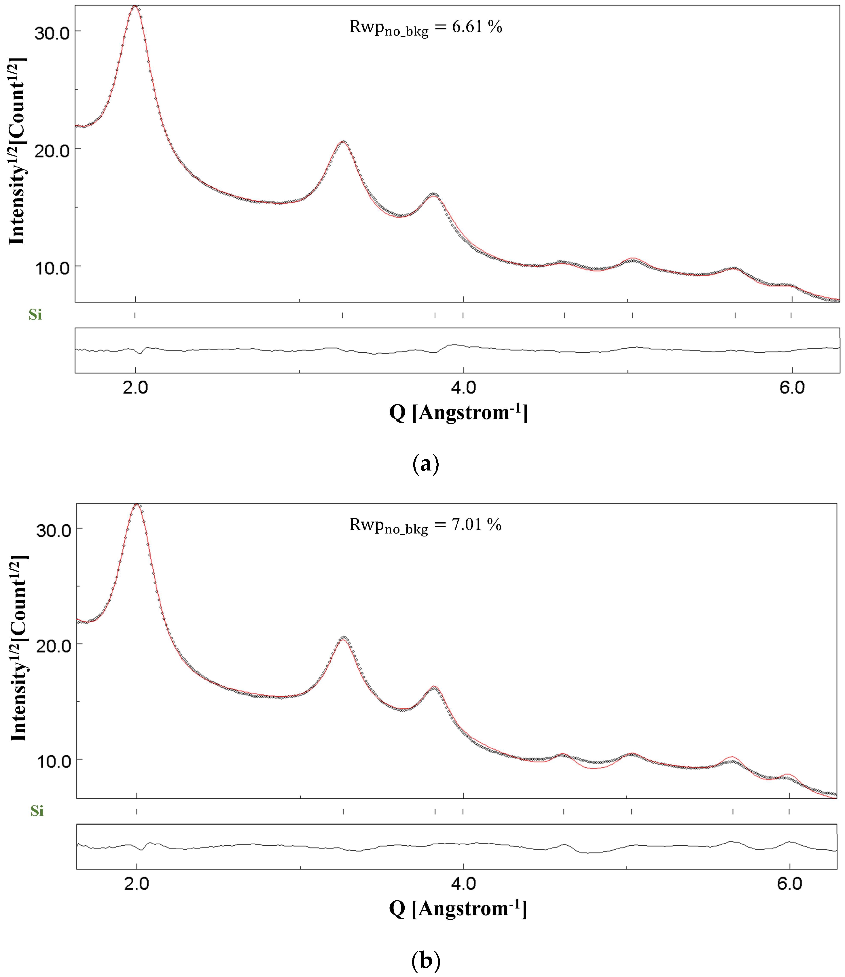
4. Results and Discussion: Rietveld Refinement of SAED Patterns
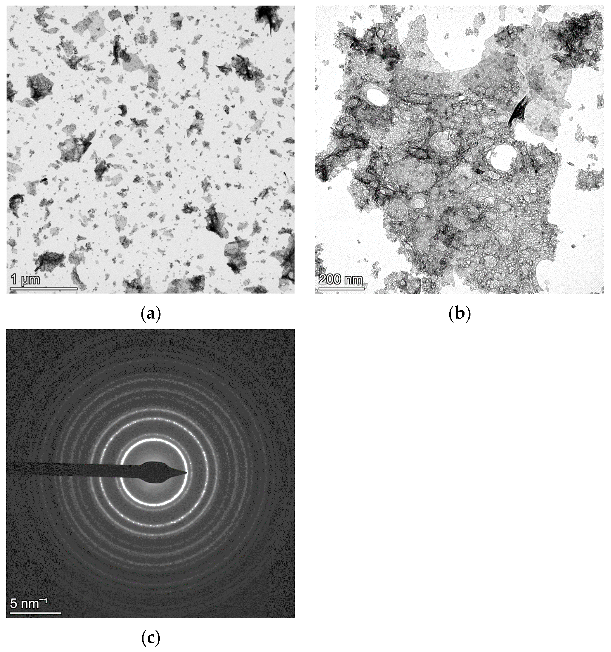
4.1. NC CeO2 and Si
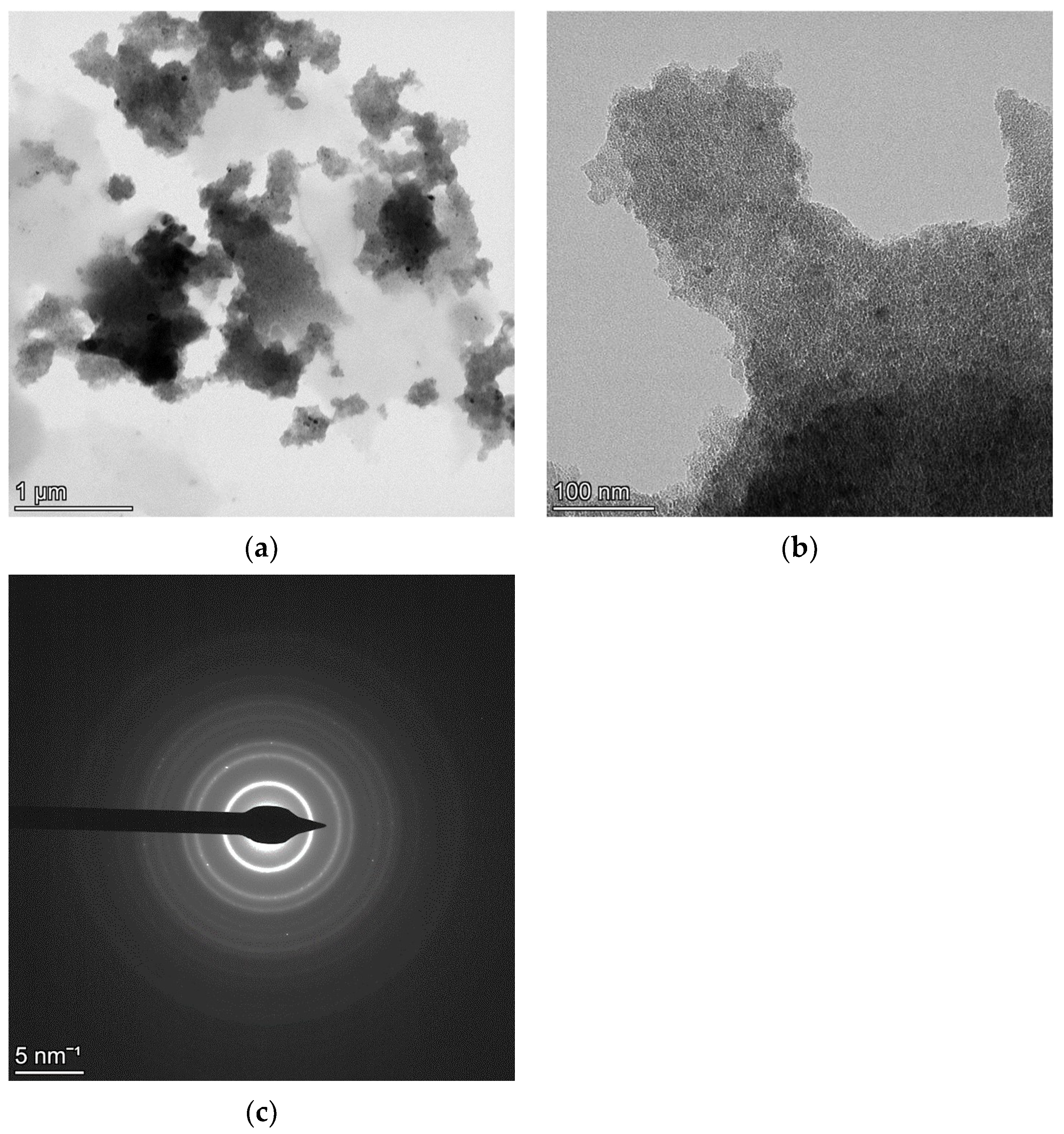
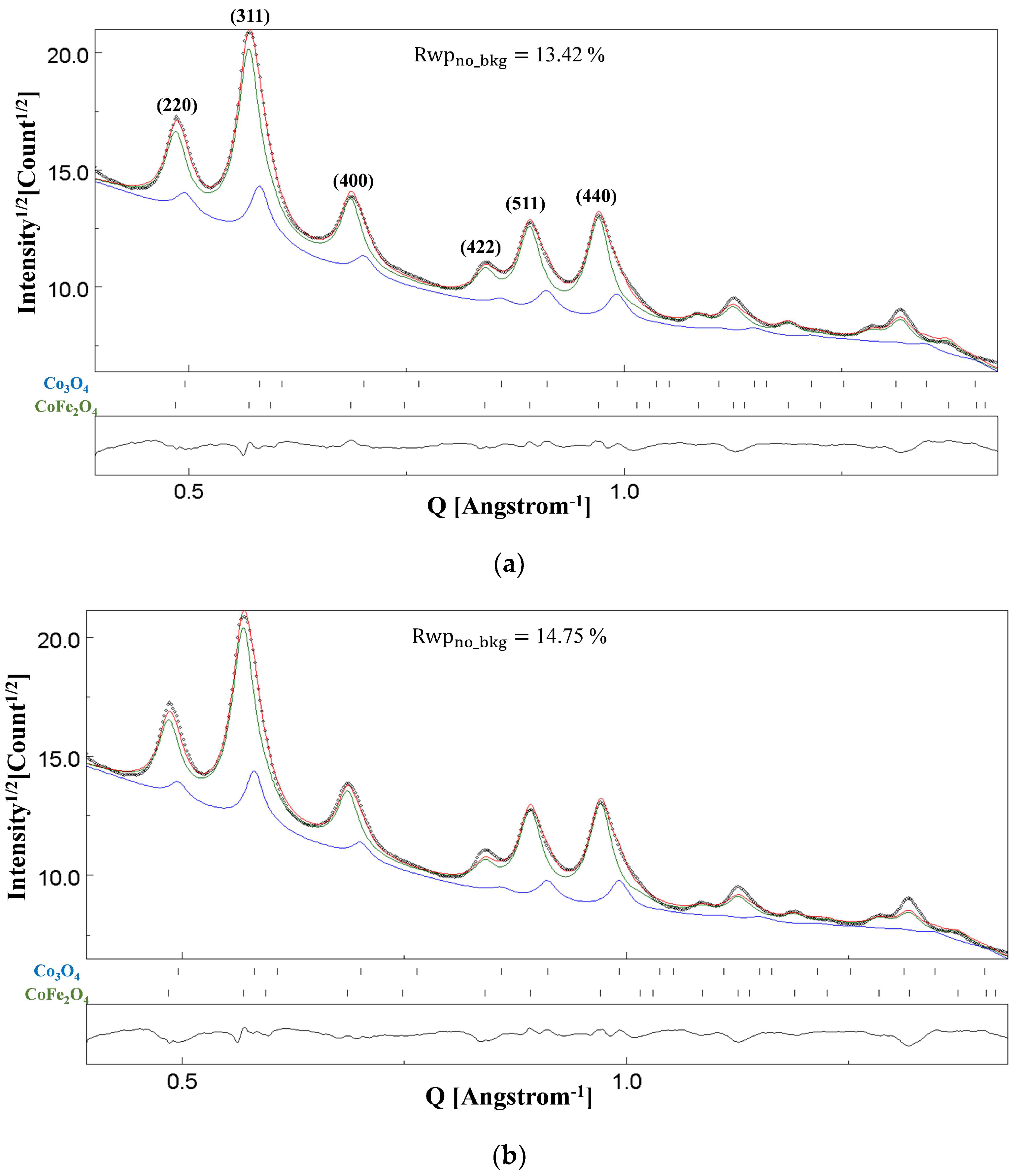
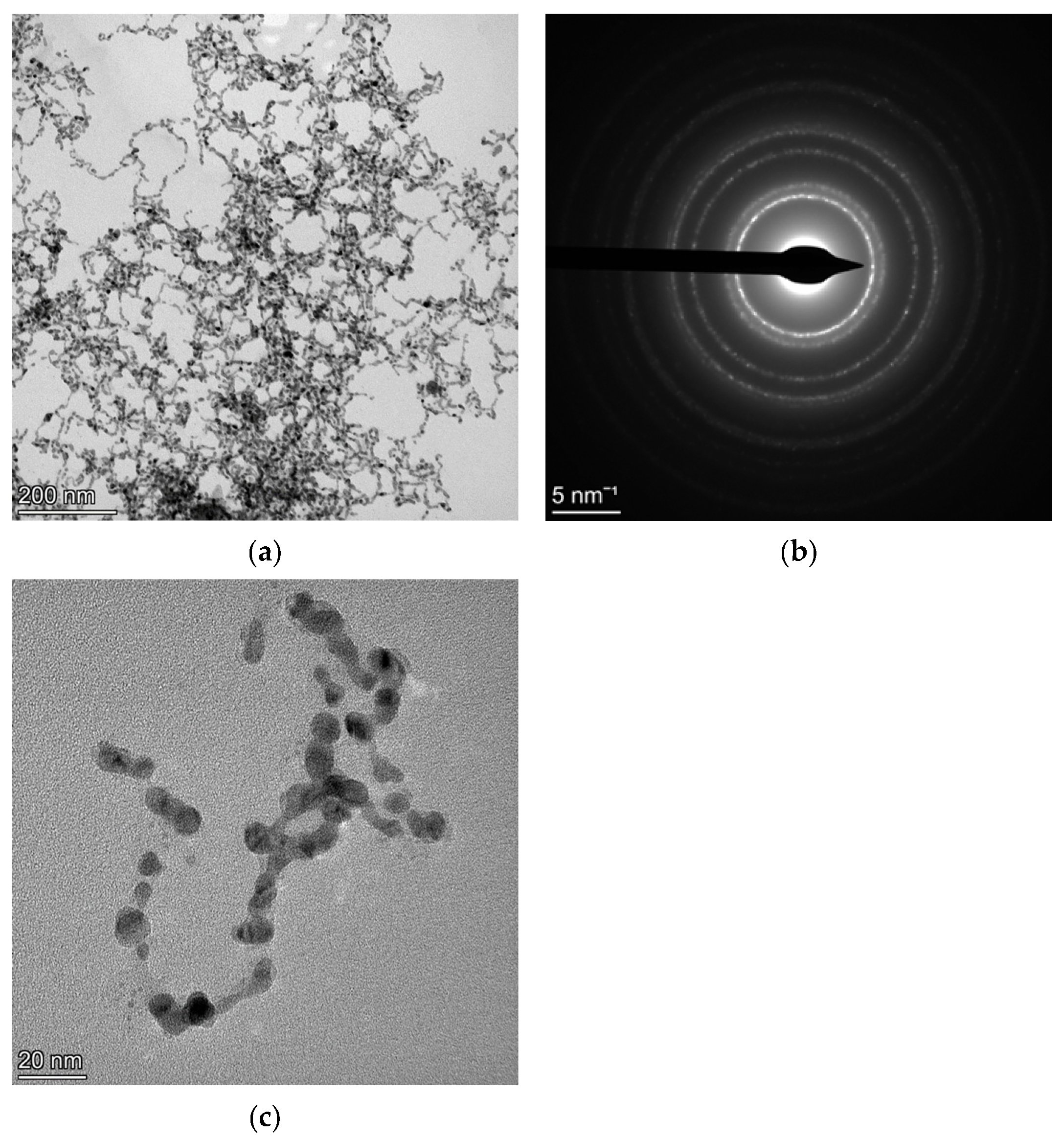
4.2. NC CoFe2O4
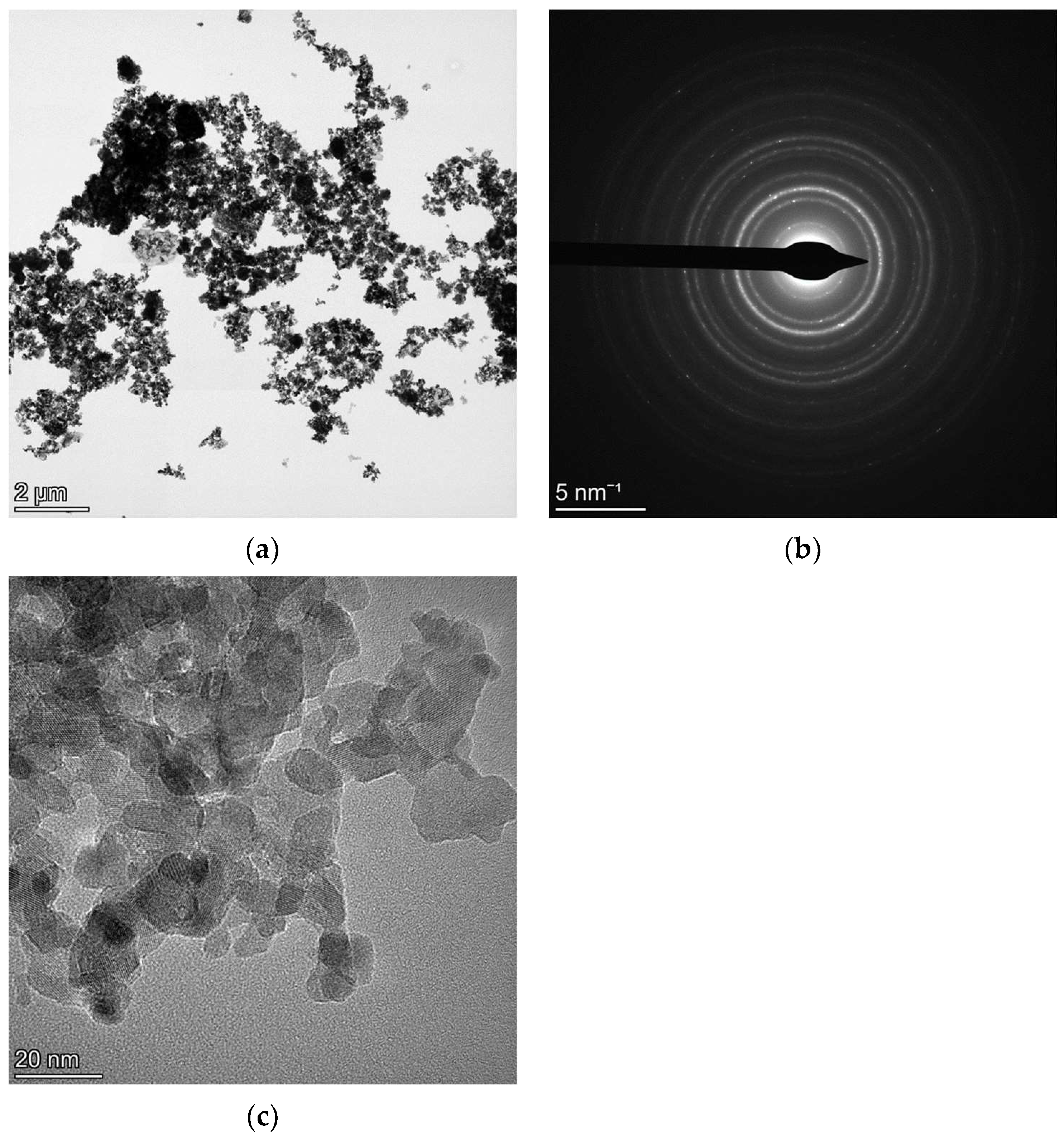
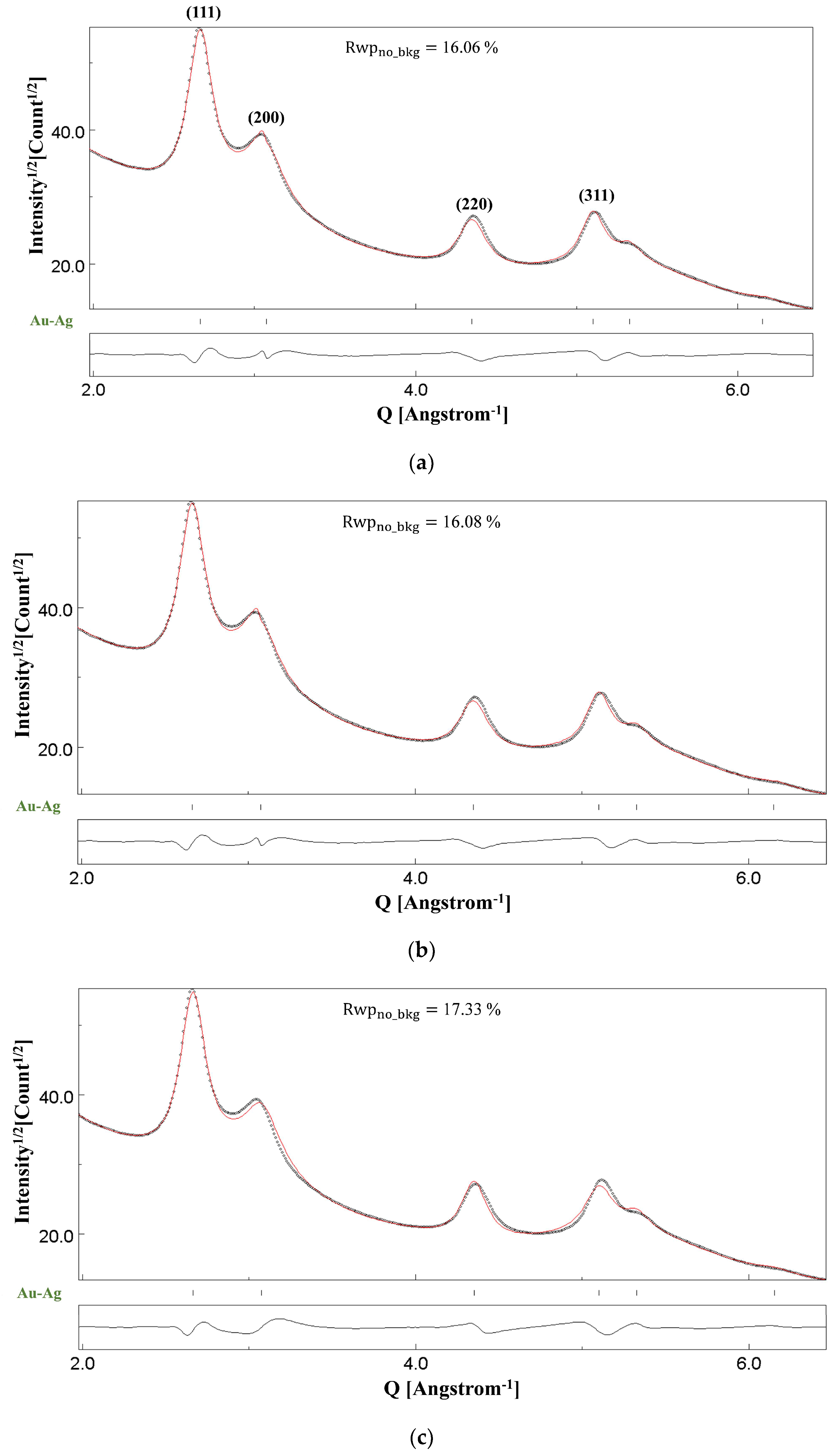
4.3. Au-Ag
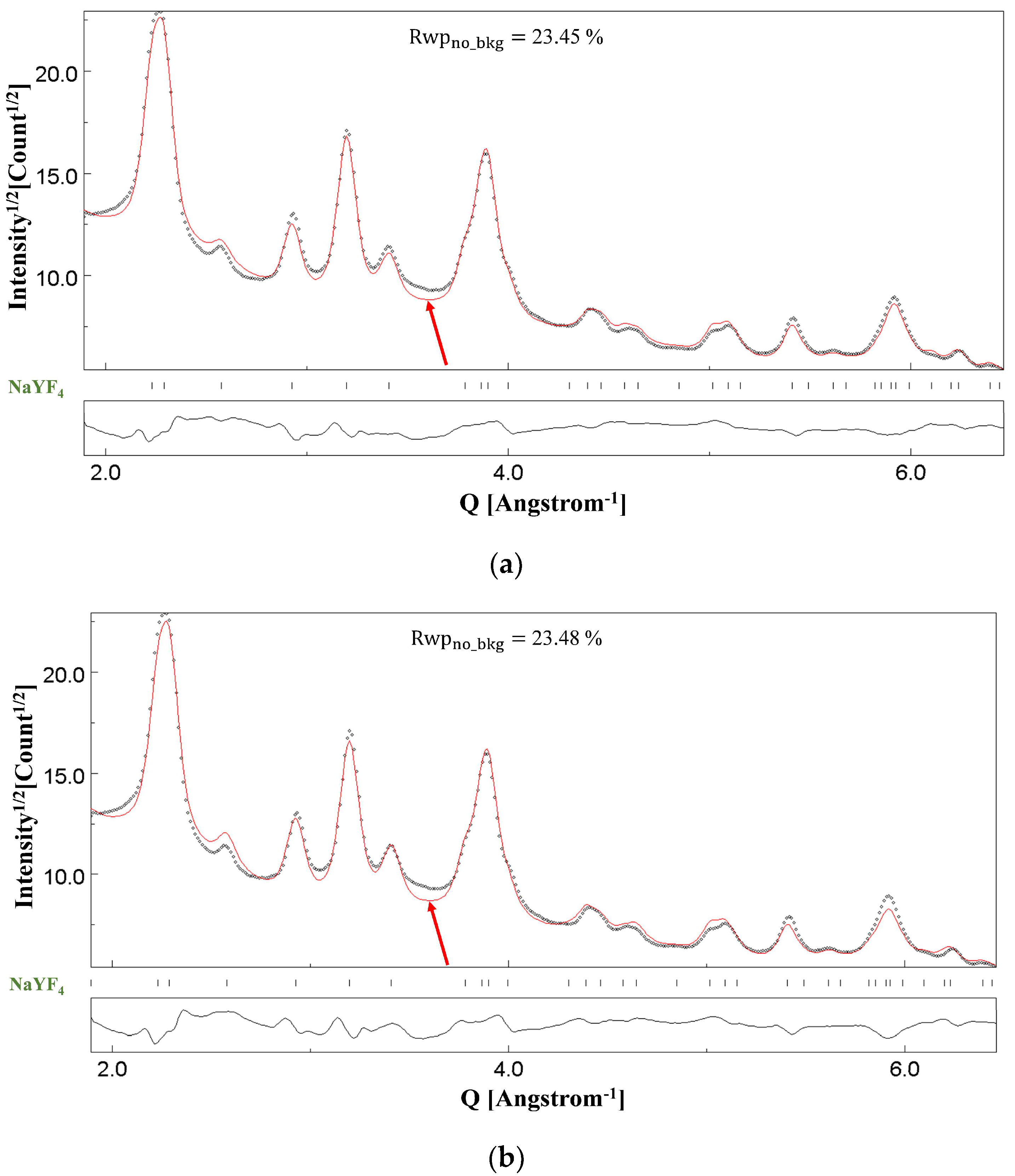
4.4. NC NaYF4
5. Conclusions and Perspectives
Author Contributions
Funding
Institutional Review Board Statement
Informed Consent Statement
Data Availability Statement
Acknowledgments
Conflicts of Interest
References
- Gleiter, H. Nanocrystalline Materials. Prog. Mater. Sci. 1989, 33, 223–315. [Google Scholar] [CrossRef]
- Vepřek, S. The Search for Novel, Superhard Materials. J. Vac. Sci. Technol. A 1999, 17, 2401–2420. [Google Scholar] [CrossRef]
- Niederhofer, A.; Bolom, T.; Nesladek, P.; Moto, K.; Eggs, C.; Patil, D.S.; Veprek, S. The Role of Percolation Threshold for the Control of the Hardness and Thermal Stability of Super- and Ultrahard Nanocomposites. Surf. Coat. Technol. 2001, 146–147, 183–188. [Google Scholar] [CrossRef]
- Lu, Y.; Liaw, P.K. The Mechanical Properties of Nanostructured Materials. JOM 2001, 53, 31–35. [Google Scholar] [CrossRef]
- Latysh, V.; Krallics, G.; Alexandrov, I.; Fodor, A. Application of Bulk Nanostructured Materials in Medicine. Curr. Appl. Phys. 2006, 6, 262–266. [Google Scholar] [CrossRef]
- Zhu, Y.T.; Lowe, T.C.; Langdon, T.G. Performance and Applications of Nanostructured Materials Produced by Severe Plastic Deformation. Scr. Mater. 2004, 51, 825–830. [Google Scholar] [CrossRef]
- Höppel, H.-W.; Mughrabi, H.; Vinogradov, A. Fatigue Properties of Bulk Nanostructured Materials. In Bulk Nanostructured Materials; John Wiley & Sons, Ltd.: Weinheim, Germany, 2009; pp. 481–500. ISBN 978-3-527-62689-2. [Google Scholar]
- Rietveld, H.M. A Profile Refinement Method for Nuclear and Magnetic Structures. J. Appl. Crystallogr. 1969, 2, 65–71. [Google Scholar] [CrossRef]
- The Rietveld Method; International Union of Crystallography Monographs on Crystallography; Oxford University Press: Oxford, NY, USA, 1995; ISBN 978-0-19-855912-2.
- Toby, B.H. Rietveld Refinement. Int. Tables Crystallogr. 2019, H, 465–472. [Google Scholar] [CrossRef]
- Serafini, A.; Lutterotti, L.; Gross, S.; Gialanella, S. Characterization of Nanograined Powder Samples Using the Rietveld Method Applied to Electron Diffraction Ring Patterns. Powder Diffr. 2017, 32, S63–S68. [Google Scholar] [CrossRef]
- Sinha, A.; Bortolotti, M.; Ischia, G.; Lutterotti, L.; Gialanella, S. Electron Diffraction Characterization of Nanocrystalline Materials Using a Rietveld-Based Approach. Part I. Methodology. J. Appl. Cryst. 2022, 55, 953–965. [Google Scholar] [CrossRef]
- Sinha, A.; Ischia, G.; Lutterotti, L.; Gialanella, S. Electron Diffraction Characterization of Nanocrystalline Materials Using a Rietveld-Based Approach. Part II. Application to Microstructural Analysis. J. Appl. Cryst. 2022, 55, 1413–1423. [Google Scholar] [CrossRef]
- Sinha, A.; Candeo, S.; Straffelini, G.; Gialanella, S. TEM Characterization of Particulate Matter Emissions from the Bedding Stage of a Cu-Free Brake Friction Material. Tribol. Int. 2023, 188, 108832. [Google Scholar] [CrossRef]
- Lábár, J.; Adamik, M.; Barna, B.P.; Czigány, Z.; Fogarassy, Z.; Horváth, Z.E.; Geszti, O.; Misják, F.; Radnóczi, G.; Sáfrán, G.; et al. Electron Diffraction Based Analysis of Phase Fractions and Texture in Nanocrystalline Thin Films, Part III: Application Examples. Microsc. Microanal. 2012, 18, 406–420. [Google Scholar] [CrossRef] [PubMed]
- Cowley, J.M.; Goodman, P.; Vainshtein, B.K.; Zvyagin, B.B.; Dorset, D.L. Electron Diffraction and Electron Microscopy in Structure Determination. In International Tables for Crystallography Volume B: Reciprocal Space; Shmueli, U., Ed.; International Tables for Crystallography; Springer: Dordrecht, The Netherlands, 2001; pp. 276–345. ISBN 978-1-4020-5407-5. [Google Scholar]
- Weirich, T.E.; Winterer, M.; Seifried, S.; Hahn, H.; Fuess, H. Rietveld Analysis of Electron Powder Diffraction Data from Nanocrystalline Anatase, TiO2. Ultramicroscopy 2000, 81, 263–270. [Google Scholar] [CrossRef]
- Zou, X.; Sukharev, Y.; Hovmöller, S. Quantitative Electron Diffraction—New Features in the Program System ELD. Ultramicroscopy 1993, 52, 436–444. [Google Scholar] [CrossRef]
- Rodriguez-Carvajal, J. FULLPROF—A Program for Rietveld, Profile Matching and Integrated Intensities Refinement of X-Ray and/or Neutron Data; Laboratoire Léon Brillouin, CEA: Saclay, France, 2000. [Google Scholar]
- Weirich, T.E.; Winterer, M.; Seifried, S.; Mayer, J. Structure of Nanocrystalline Anatase Solved and Refined from Electron Powder Data. Acta Cryst. A 2002, 58, 308–315. [Google Scholar] [CrossRef] [PubMed]
- Kim, J.-G.; Seo, J.-W.; Cheon, J.-W.; Kim, Y.-J. Rietveld Analysis of Nano-Crystalline MnFe2O4 with Electron Powder Diffraction. Bull. Korean Chem. Soc. 2009, 30, 183–187. [Google Scholar] [CrossRef]
- Song, K.; Kim, Y.-J.; Kim, Y.-I.; Kim, J.-G. Application of Theta-Scan Precession Electron Diffraction to Structure Analysis of Hydroxyapatite Nanopowder. J. Electron. Microsc. 2012, 61, 9–15. [Google Scholar] [CrossRef]
- Tonejc, A.M.; Djerdj, I.; Tonejc, A. An Analysis of Evolution of Grain Size-Lattice Parameters Dependence in Nanocrystalline TiO2 Anatase. Mater. Sci. Eng. C 2002, 19, 85–89. [Google Scholar] [CrossRef]
- Lábár, J.L. ProcessDiffraction: A Computer Program to Process Electron Diffraction Patterns from Polycrystalline or Amorphous Samples. Proc. Proc. Eurem. 2000, 12, 1397. [Google Scholar]
- Oleynikov, P.; Hovmöller, S.; Zou, X.; Zhukhlistov, A.P.; Nickolsky, M.S.; Zvyagin, B.B. TexPat—A Program for Quantitative Analysis of Oblique Texture Electron Diffraction Patterns. Z. Für Krist.-Cryst. Mater. 2004, 219, 12–19. [Google Scholar] [CrossRef]
- Gemmi, M.; Voltolini, M.; Ferretti, A.M.; Ponti, A. Quantitative Texture Analysis from Powder-like Electron Diffraction Data. J. Appl. Cryst. 2011, 44, 454–461. [Google Scholar] [CrossRef]
- Lutterotti, L. Total Pattern Fitting for the Combined Size–Strain–Stress–Texture Determination in Thin Film Diffraction. Nucl. Instrum. Methods Phys. Res. Sect. B Beam Interact. Mater. At. 2010, 268, 334–340. [Google Scholar] [CrossRef]
- Lutterotti, L.; Matthies, S.; Wenk, H.-R.; Schultz, A.S.; Richardson, J.W. Combined Texture and Structure Analysis of Deformed Limestone from Time-of-Flight Neutron Diffraction Spectra. J. Appl. Phys. 1997, 81, 594–600. [Google Scholar] [CrossRef]
- Stadelmann, P. Image Analysis and Simulation Software in Transmission Electron Microscopy. Microsc. Microanal. 2003, 9, 60–61. [Google Scholar] [CrossRef]
- Blackman, M.; Thomson, G.P. On the Intensities of Electron Diffraction Rings. Proc. R. Soc. London. Ser. A. Math. Phys. Sci. 1939, 173, 68–82. [Google Scholar] [CrossRef]
- Li, X.Z. JECP/PCED—A Computer Program for Simulation of Polycrystalline Electron Diffraction Pattern and Phase Identification. Ultramicroscopy 2004, 99, 257–261. [Google Scholar] [CrossRef]
- Li, X.-Z. QPCED2.0: A Computer Program for the Processing and Quantification of Polycrystalline Electron Diffraction Patterns. J. Appl. Cryst. 2012, 45, 862–868. [Google Scholar] [CrossRef]
- Lábár, J.L. Electron Diffraction Based Analysis of Phase Fractions and Texture in Nanocrystalline Thin Films, Part I: Principles. Microsc. Microanal. 2008, 14, 287–295. [Google Scholar] [CrossRef]
- Lábár, J.L. Electron Diffraction Based Analysis of Phase Fractions and Texture in Nanocrystalline Thin Films, Part II: Implementation. Microsc. Microanal. 2009, 15, 20–29. [Google Scholar] [CrossRef] [PubMed]
- Boullay, P.; Lutterotti, L.; Chateigner, D.; Sicard, L. Fast Microstructure and Phase Analyses of Nanopowders Using Combined Analysis of Transmission Electron Microscopy Scattering Patterns. Acta Cryst. A 2014, 70, 448–456. [Google Scholar] [CrossRef] [PubMed]
- Abram, V.; Sinha, A.; Lutterotti, L.; Gialanella, S. Mathematics of Two-Beam Dynamical Correction Implementation in Material Analysis Using Diffraction (MAUD). Department of Industrial Engineering, University of Trento, Trento, Italy. 2025; in preparation. [Google Scholar]
- Self, P.G.; O’Keefe, M.A.; Buseck, P.R.; Spargo, A.E.C. Practical Computation of Amplitudes and Phases in Electron Diffraction. Ultramicroscopy 1983, 11, 35–52. [Google Scholar] [CrossRef]
- Peng, L.-M. Electron Atomic Scattering Factors and Scattering Potentials of Crystals. Micron 1999, 30, 625–648. [Google Scholar] [CrossRef]
- Sinkler, W.; Own, C.S.; Marks, L.D. Application of a 2-Beam Model for Improving the Structure Factors from Precession Electron Diffraction Intensities. Ultramicroscopy 2007, 107, 543–550. [Google Scholar] [CrossRef]
- Li, X.Z. PCED2.0—A Computer Program for the Simulation of Polycrystalline Electron Diffraction Pattern. Ultramicroscopy 2010, 110, 297–304. [Google Scholar] [CrossRef] [PubMed]
- Peng, L.-M.; Ren, G.; Dudarev, S.L.; Whelan, M.J. Robust Parameterization of Elastic and Absorptive Electron Atomic Scattering Factors. Acta Cryst. A 1996, 52, 257–276. [Google Scholar] [CrossRef]
- Lábár, J.L. Consistent Indexing of a (Set of) Single Crystal SAED Pattern(s) with the Process Diffraction Program. Ultramicroscopy 2005, 103, 237–249. [Google Scholar] [CrossRef]
- Lutterotti, L.; Vasin, R.; Wenk, H.-R. Rietveld Texture Analysis from Synchrotron Diffraction Images. I. Calibration and Basic Analysis. Powder Diffr. 2014, 29, 76–84. [Google Scholar] [CrossRef]
- Tsubota, M.; Kitagawa, J. A Necessary Criterion for Obtaining Accurate Lattice Parameters by Rietveld Method. Sci. Rep. 2017, 7, 15381. [Google Scholar] [CrossRef] [PubMed]
- Pini, F.; Pilot, R.; Ischia, G.; Agnoli, S.; Amendola, V. Au–Ag Alloy Nanocorals with Optimal Broadband Absorption for Sunlight-Driven Thermoplasmonic Applications. ACS Appl. Mater. Interfaces 2022, 14, 28924–28935. [Google Scholar] [CrossRef]
- Zuo, J.-M.; Lábár, J.L.; Zhang, J.; Gorelik, T.E.; Kolb, U. Electron Powder Diffraction; International Union of Crystallography: Chester UK, 2019; Volume H, Chapter 2.4; pp. 102–117. [Google Scholar]
- Trueblood, K.N.; Bürgi, H.-B.; Burzlaff, H.; Dunitz, J.D.; Gramaccioli, C.M.; Schulz, H.H.; Shmueli, U.; Abrahams, S.C. Atomic Dispacement Parameter Nomenclature. Report of a Subcommittee on Atomic Displacement Parameter Nomenclature. Acta Cryst. A 1996, 52, 770–781. [Google Scholar] [CrossRef]
- Reimer, L. Transmission Electron Microscopy; Springer Series in Optical Sciences; Springer: Berlin/Heidelberg, Germany, 1989; Volume 36, ISBN 978-3-540-50499-3. [Google Scholar]
- Varma, P.C.R.; Manna, R.S.; Banerjee, D.; Varma, M.R.; Suresh, K.G.; Nigam, A.K. Magnetic Properties of CoFe2O4 Synthesized by Solid State, Citrate Precursor and Polymerized Complex Methods: A Comparative Study. J. Alloys Compd. 2008, 453, 298–303. [Google Scholar] [CrossRef]
- Popa, N.C. The (Hkl) Dependence of Diffraction-Line Broadening Caused by Strain and Size for All Laue Groups in Rietveld Refinement. J. Appl. Cryst. 1998, 31, 176–180. [Google Scholar] [CrossRef]
- Kondarides, D.I.; Verykios, X.E. Interaction of Oxygen with Supported Ag–Au Alloy Catalysts. J. Catal. 1996, 158, 363–377. [Google Scholar] [CrossRef]
- Wang, A.-Q.; Liu, J.-H.; Lin, S.D.; Lin, T.-S.; Mou, C.-Y. A Novel Efficient Au–Ag Alloy Catalyst System: Preparation, Activity, and Characterization. J. Catal. 2005, 233, 186–197. [Google Scholar] [CrossRef]
- Gražulis, S.; Chateigner, D.; Downs, R.T.; Yokochi, A.F.T.; Quirós, M.; Lutterotti, L.; Manakova, E.; Butkus, J.; Moeck, P.; Le Bail, A. Crystallography Open Database–an open-access collection of crystal structures. J. Appl. Cryst. 2009, 42, 726–729. [Google Scholar] [CrossRef]
- Warren, B.E. X-Ray Diffraction; Addison-Wesley: Reading, MA, USA, 1969. [Google Scholar]
- Lutterotti, L.; Gialanella, S. X-Ray Diffraction Characterization of Heavily Deformed Metallic Specimens. Acta Mater. 1998, 46, 101–110. [Google Scholar] [CrossRef]
- Gialanella, S.; Amils, X.; Barò, M.D.; Delcroix, P.; Le Caër, G.; Lutterotti, L.; Suriñach, S. Microstructural and Kinetic Aspects of the Transformations Induced in a FeAl Alloy by Ball-Milling and Thermal Treatments. Acta Mater. 1998, 46, 3305–3316. [Google Scholar] [CrossRef]
- Yuming, W.; Ziqung, Z. X-Ray Line Profile Analysis of Dislocations and Stacking Faults in Deformed Copper. Appl. Phys. A 1984, 35, 109–114. [Google Scholar] [CrossRef]
- Grzechnik, A.; Bouvier, P.; Mezouar, M.; Mathews, M.D.; Tyagi, A.K.; Köhler, J. Hexagonal Na1.5Y1.5F6 at High Pressures. J. Solid State Chem. 2002, 165, 159–164. [Google Scholar] [CrossRef]
- Ashby, M.F.; Ferreira, P.J.; Schodek, D.L. Chapter 6—Nanomaterials: Classes and Fundamentals. In Nanomaterials, Nanotechnologies and Design; Ashby, M.F., Ferreira, P.J., Schodek, D.L., Eds.; Butterworth-Heinemann: Boston, MA, USA, 2009; pp. 177–197. ISBN 978-0-7506-8149-0. [Google Scholar]
- Ulvestad, A.; Yau, A. The Self-Healing of Defects Induced by the Hydriding Phase Transformation in Palladium Nanoparticles. Nat. Commun. 2017, 8, 1376. [Google Scholar] [CrossRef] [PubMed]


| Symbol | Meaning |
|---|---|
| cell volume | |
| electron mass | |
| electron charge | |
| wave vector of the incident electron | |
| energy of the electron | |
| q-th Fourier coefficient of the potential V | |
| thickness of the sample or crystal | |
| -th extinction distance |
| Plane | FDYN (Å) | FKIN (Å) | RatioF |
|---|---|---|---|
| 111 | 160.06 | 152.64 | 1.05 |
| 200 | 92.37 | 89.79 | 1.03 |
| 220 | 180.61 | 171.32 | 1.05 |
| 311 | 164.43 | 156.67 | 1.05 |
| 222 | 59.29 | 58.22 | 1.02 |
| 400 | 83.45 | 81.36 | 1.03 |
| 331 | 110.25 | 106.66 | 1.03 |
| 420 | 68.16 | 66.76 | 1.02 |
| Plane | FDYN (Å) | FKIN (Å) | RatioF |
|---|---|---|---|
| 111 | 34.44 | 69.38 | 0.50 |
| 220 | 33.27 | 54.97 | 0.61 |
| 311 | 28.38 | 44.39 | 0.64 |
| 400 | 15.79 | 25.18 | 0.63 |
| 331 | 18.36 | 32.57 | 0.56 |
| 422 | 19.79 | 41.27 | 0.48 |
| Phase | Lattice Parameter a (Å) | Crystallite Size (Å) | Atomic Occupancy | Atomic Position (Oxygen) | Phase Fraction (%) | Thickness (Å) | Rwpno_bkg (%) |
|---|---|---|---|---|---|---|---|
| CoFe2O4 | 8.383 | 76.9(6) | Co: 0.032 Fe: 0.967(5) | 0.3815(4) | 79.74 | 1588(24) | 13.42 |
| Co3O4 | 8.20 | 82(2) | Co: 0.97 Fe: 0.03(40) | - | 20.26 |
| Phase | Lattice Parameter a (Å) | Crystallite Size (Å) | Atomic Occupancy | Atomic Position (Oxygen) | Phase Fraction (%) | Rwpno_bkg (%) |
|---|---|---|---|---|---|---|
| CoFe2O4 | 8.380 | 75.9(2) | Co: 0.048 Fe: 0.951(5) | 0.3896(2) | 82.75 | 14.75 |
| Co3O4 | 8.20 | 96(1) | Co: 0.98 Fe: 0.02(40) | - | 17.25 |
| Lattice Parameter (Å) and Atomic Occupancy of Au | Crystallite Size, Average (Å) | Anisotropic Crystallite Size (Å) | Thickness (Å) | Rwpno_bkg (%) |
|---|---|---|---|---|
| 4.08; 0.91(7) | 127(6) | [200]: 35 [420]: 81 | 83(26) | 16.06 |
| Lattice Parameter (Å) and Atomic Occupancy of Au | Crystallite Size, Average (Å) | Anisotropic Crystallite Size (Å) | Rwpno_bkg (%) |
|---|---|---|---|
| 4.08; 0.90(1) | 126(2) | [200]: 35 [420]: 81 | 16.08 |
| Intrinsic Deformation Fault Probability (α′) | Extrinsic Deformation Fault Probability (α″) | Twin Fault Probability (β′) |
|---|---|---|
| 0.050(2) | 0.001(1) | 0.002(6) |
| Lattice Parameter (Å) | Refined Atomic Positions | Crystallite Size, Average (Å) | Thickness (Å) | Rwpno_bkg (%) |
|---|---|---|---|---|
| Na (2)—z: 0.438(7) | 142(1) | 139(44) | 23.45 | |
| a: 5.6298(6) | F (1)—x: 0.666(1); y: 0.086(2) | |||
| c: 3.3221(6) | F (2)—x: 0.712(1); y: 0.756(2) |
| Lattice Parameter (Å) | Refined Atomic Positions | Crystallite Size, Average (Å) | Rwpno_bkg (%) |
|---|---|---|---|
| Na (2)—z: 0.439(7) | 140(1) | 23.48 | |
| a: 5.6296(6) | F (1)—x: 0.665(1); y: 0.084(2) | ||
| c: 3.3220(5) | F (2)—x: 0.714(1); y: 0.759(2) |
| Material | Thickness Parameter, T (Å) |
|---|---|
| CeO2 | 45(1) |
| Si | 5008(42) |
| CoFe2O4 | 1588(24) |
| Au-Ag | 83(26) |
| NaYF4 | 139(44) |
Disclaimer/Publisher’s Note: The statements, opinions and data contained in all publications are solely those of the individual author(s) and contributor(s) and not of MDPI and/or the editor(s). MDPI and/or the editor(s) disclaim responsibility for any injury to people or property resulting from any ideas, methods, instructions or products referred to in the content. |
© 2025 by the authors. Licensee MDPI, Basel, Switzerland. This article is an open access article distributed under the terms and conditions of the Creative Commons Attribution (CC BY) license (https://creativecommons.org/licenses/by/4.0/).
Share and Cite
Sinha, A.; Abram, V.; Lutterotti, L.; Gialanella, S. Rietveld Refinement of Electron Diffraction Patterns of Nanocrystalline Materials Using MAUD: Two-Beam Dynamical Correction Implementation and Applications. Materials 2025, 18, 650. https://doi.org/10.3390/ma18030650
Sinha A, Abram V, Lutterotti L, Gialanella S. Rietveld Refinement of Electron Diffraction Patterns of Nanocrystalline Materials Using MAUD: Two-Beam Dynamical Correction Implementation and Applications. Materials. 2025; 18(3):650. https://doi.org/10.3390/ma18030650
Chicago/Turabian StyleSinha, Ankur, Valentino Abram, Luca Lutterotti, and Stefano Gialanella. 2025. "Rietveld Refinement of Electron Diffraction Patterns of Nanocrystalline Materials Using MAUD: Two-Beam Dynamical Correction Implementation and Applications" Materials 18, no. 3: 650. https://doi.org/10.3390/ma18030650
APA StyleSinha, A., Abram, V., Lutterotti, L., & Gialanella, S. (2025). Rietveld Refinement of Electron Diffraction Patterns of Nanocrystalline Materials Using MAUD: Two-Beam Dynamical Correction Implementation and Applications. Materials, 18(3), 650. https://doi.org/10.3390/ma18030650