Article

Process Parameters Analysis in Diamond Wire Saw Cutting NdFeB Magnet

by
Chengwanli Peng
1,
Guanzheng Li
2,
Xingchun Zhang
2 and
Yufei Gao
2,3,4,*
1
SDU-ANU Joint Science College, Shandong University, Weihai 264209, China
2
Key Laboratory of High Efficiency and Clean Mechanical Manufacture of MOE, School of Mechanical Engineering, Shandong University, Jinan 250061, China
3
State Key Laboratory of Advanced Equipment and Technology for Metal Forming, Shandong University, Jinan 250061, China
4
Shandong Key Laboratory of High Performance Tools and System, Shandong University, Jinan 250061, China
*
Author to whom correspondence should be addressed.
Materials 2025, 18(5), 1173; https://doi.org/10.3390/ma18051173
Submission received: 14 February 2025 / Revised: 28 February 2025 / Accepted: 5 March 2025 / Published: 6 March 2025
(This article belongs to the Section Manufacturing Processes and Systems)

Abstract

:
Neodymium iron boron (NdFeB) magnetic materials are widely used in fields such as electronics, medical devices, power machinery, and hardware machinery. This paper conducted a three-factor and five-level orthogonal experiment on diamond wire saw cutting NdFeB to determine the influence degree of key factors such as workpiece feed rate, diamond wire speed, and workpiece processed size on the surface roughness Ra and waviness Wa of NdFeB slices. Further analysis was conducted on the influence of various parameters on the PV value (peak valley difference) of the waviness profile curve of the sawed surface. Finally, slicing processing was carried out under optimized process parameter combinations. The research results indicate that the primary and secondary order of process parameters affecting surface roughness Ra and waviness Wa is workpiece feed rate, wire speed, and sawed workpiece size, and the influence on the waviness PV value also shows a consistent trend. The optimal combination of processing parameters is workpiece feed rate of 0.1 mm·min−1, wire speed of 1600 m·min−1, and workpiece size of 10 mm. The obtained surface roughness Ra is 0.433 μm and the waviness Wa is 0.037 μm, respectively. The regression mathematical model for the waviness PV value is PV = 0.747 × vs−0.342 × vw0.546 × L0.109. The research results of this paper provide an experimental basis and guidance for optimizing process parameters of sawing NdFeB.

1. Introduction

Neodymium iron boron (NdFeB) magnetic materials are widely used in fields such as electronics, medical devices, power machinery, and hardware machinery. In recent years, NdFeB plays a more important role in new energy, wind power generation, communication technology, aerospace, and other fields, and its demand is constantly increasing [1,2]. The production process of NdFeB magnets mainly includes sintering powdered raw materials into blank blocks, and then cutting them into slices, which are then surface ground and electroplated to produce the final product. Figure 1 shows the several typical preparation stages of NdFeB magnets. The final process of NdFeB magnets is electroplating, which mainly makes their surface smoother and more beautiful, less prone to oxidation and corrosion, and extends their service life. Before electroplating, NdFeB slices generally need to be ground to improve surface quality. Therefore, the surface characteristics formed in the NdFeB slicing process directly affect the workload and cost of subsequent grinding processing.
Wire electrical discharge machining (WEDM) is the earliest method used for slicing NdFeB, and scholars’ research mainly involves temperature field analysis of NdFeB magnetism in WEDM, material removal mechanism, and the influence of WEDM process parameters [3,4,5,6]. These studies have found that WEDM-cut NdFeB magnet surfaces exhibit defects such as cracks, craters, and melting. Due to thermal effects during the cutting process, oxidation occurs on the cut surface, leading to an 18.9% increase in oxygen content. Some neodymium and iron elements exist in the form of oxides, such as FeO and Nd2O3 [3]. The depth of the heat-affected zone can reach up to 35 μm [4]. The minimum roughness Ra is about 2 μm [5,6]. Laser cutting is another cutting NdFeB process. Wang et al. [7] studied the effect of laser cutting on the internal structure and properties of sintered NdFeB, and found that the structure in the laser cutting area is damaged due to the high-temperature effect of the laser beam. The cut area presents obvious laser cutting textures, and its surface roughness is six–seven times that of wire saw cutting. Ren et al. [8] numerically simulated the laser cutting temperature distribution of NdFeB using the finite element method, the research results found that the instantaneous temperature in the cut area can exceed 1500 °C. Ma et al. [9] found that the laser-cut NdFeB surface roughness exceeded 10 μm. Laser processing has the advantages of small cutting kerf and fast cutting speed, but due to the poor thermal resistance of NdFeB, it is easy to cause more surface cracks and larger surface roughness, and the cutting can lead to a 19.8% increase in oxygen content on the surface [3]. In addition, the cost of laser processing is high, so it has not been widely used in processing of NdFeB. Wet abrasive waterjet (WAWJ) cutting can effectively avoid the influence of cutting thermal damage, but the surface roughness is generally higher than 8 μm [3].
In recent years, the diamond wire saw cutting technology, which has the advantages of low cutting loss, high processing efficiency, environmental friendliness, and relatively low cost [10,11,12,13], has become the main cutting process of NdFeB. This process removes materials by diamond abrasives fixed on a steel wire surface. In fact, diamond wire saw technology has been widely used in cutting as mono-Si [11,14], poly-Si [15], sapphire [16,17], ceramics [18,19], and composite materials [20,21,22]. Moreover, scholars have conducted extensive research on the application of diamond cutting technology in these fields. Relatively, research on NdFeB magnet cutting is still insufficient. Liu et al. [23] conducted the diamond wire sawing experiment of NdFeB magnets, and found that the surface roughness Ra can reach 0.6 μm. Wu et al. [24] designed cutting experiments and analyzed the influence of different process parameters on the surface quality of NdFeB. However, the parameter values selected in the above sawing experiments are relatively low, which differs significantly in actual industrial production. Our research group conducted a single-factor experimental analysis of wire saw cutting NdFeB by using process parameters values in industrial production. The experimental results showed that the surface roughness was mostly within the range of 1~3 μm [25]. It is necessary to reduce the surface roughness of slices by optimizing process parameters. Costa et al. [26] conducted an NdFeB scratching test, and found that as the scratching depth increased, the material removal underwent a transition from ductile to brittle.
Scholars have conducted many studies on the influence of diamond wire saw cutting process parameters on the sawed surface characteristics, which mainly focus on the sawed surface morphology characteristics and surface roughness. The concerned process parameters mainly include saw wire speed and feed rate, as well as parameters such as diamond wire tension and abrasive size. Sopori et al. [27] found that wire speed and feed rate have a significant impact on the characteristics of the cut surface. Gupta et al. [28] found that high wire speed reduces the surface roughness and subsurface damage depth of slices. Costa et al. [29] and Wang et al. [30] obtained similar conclusions for sawing mono-Si. Guo et al. [31,32] believe that increasing the wire speed and reducing the workpiece feed rate are beneficial for improving the wire bow and cutting force during sawing, thereby improving the cut surface quality. The above studies have found that the wire saw cut surface roughness is less than 2 μm. Yin et al. [33] and Liedke et al. [34] also found that when sawing workpieces with different sizes, the surface morphology and roughness also vary. Workpieces with different sizes result in different material removal rates under the same set of process parameters. In addition, when the workpiece size changes, lubrication, cooling, chip removal, and other issues during the cutting process will also change, which will affect the material removal characteristics. Therefore, the processed NdFeB size should also be considered as one of the factors.
Additionally, the surface saw marks in diamond wire sawing have attracted the attention of scholars. The saw marks present a periodic waviness along the workpiece feed direction [35], which has a significant impact on the processed surface quality and increases the cost of subsequent processing steps. In the study of sawing silicon wafers, it was found that the stress concentration caused by periodic waviness can reduce the mechanical properties of the wafer, thereby increasing the probability of wafer fracture along the saw mark [36]. In addition, the periodic waviness has a greater impact on slice warpage [37]. Therefore, reducing the waviness has positive significance for improving wafer quality and reducing the workload of subsequent processes.
Early research by Teomet [38] suggested that periodic waviness on the sawed surface were caused by random lateral forces generated by abrasives on the diamond wire surface during sawing. The lateral forces caused the diamond wire to oscillate laterally in the saw kerf, and an increase in feed rate resulted in higher peak-valley values. Lai et al. [35] found that the periodic saw marks on the sawed surface of sapphire crystals were related to the reciprocating operation of diamond wire. This discovery was also proposed in experiments of cutting NdFeB magnets [23,24,25]. Liu et al. [23] and Wu et al. [24] found the PV value (peak-valley difference) of the waviness profile curve of the sawed surface is around 1.5~8 μm. However, the parameter values used are generally low, such as a maximum wire speed about 100 m·min−1. Qiu et al. [11] believed that periodic saw marks were affected by the wire bow and wire lateral swing. The reciprocating moving of diamond wire can cause fluctuations in the material removal behavior on both sides, resulting in periodic changes in the cut width and causing saw marks. Regarding the improvement of saw marks, Li et al. [39] conducted research on a new diamond wire cutting process. However, there is currently little research on optimizing process parameters for improving saw marks.
Overall, there is a lack of systematic experimental research on the optimization of sawing process parameter combinations in diamond wire saw slicing NdFeB, which is of great significance for improving the surface quality and reducing the subsequent processing cost. This paper conducted a three-factor and five-level orthogonal experiment on diamond wire saw cutting NdFeB by using the parameter values in industrial production. The impact of key factors, such as workpiece feed rate, saw wire speed, and workpiece size, on the surface roughness Ra and waviness Wa of slices was determined through range analysis of the experimental results. Further analysis was conducted on the influence of various parameters on the PV value of waviness profile curve of sawed surface. Finally, the optimized process parameter combination was determined, providing experimental basis and guidance for sawing NdFeB.

2. Materials and Methods

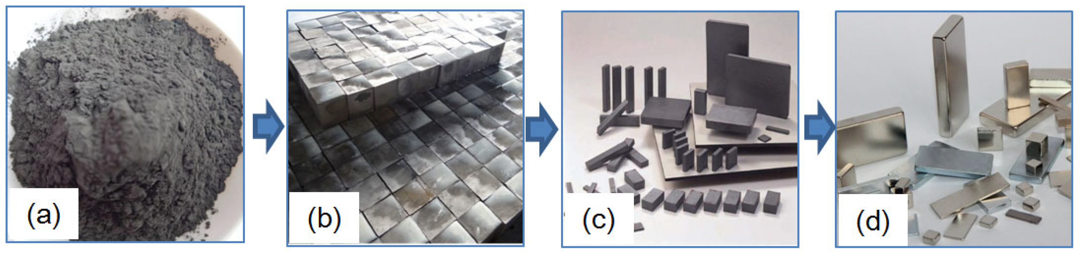
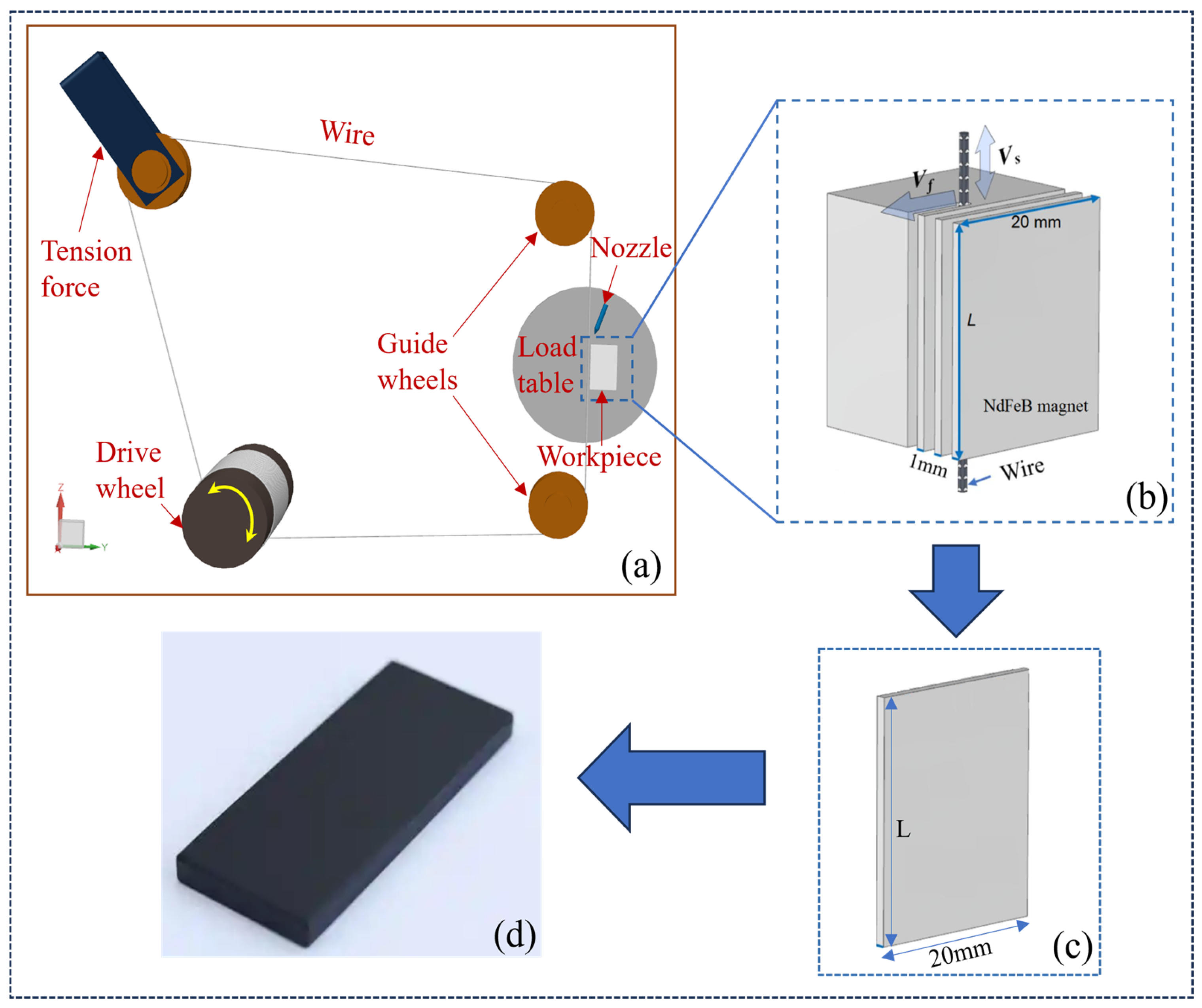
2.1. Experimental Materials and Equipment

The wire sawing experiments were conducted on a diamond single-wire cutting machine (SH300, Guangzhou Shenghai Electronic Technology Co., Ltd., Guangzhou, China), and its appearance can be seen in our previously published paper [25]. A schematic diagram of the machine tool is shown in Figure 2a. The diamond wire is guided by two guide pulleys, and then wound onto the drive roller, with tension applied by a tension pulley using gravity. During the cutting process, the wire wound on the drive roller moves reciprocally at a set speed Vs, while the load table feeds at a predetermined speed Vw to drive the NdFeB to press the wire. During sawing, tap water was used as the cutting fluid, and the nozzle sprays tap water onto the cutting area to achieve cooling and lubrication.
N35-sintered NdFeB rectangular magnets (provided by Ningbo Xinlin Magnetic Industry Co., Ltd., Ningbo, China) were adopted in the experiment, with a cut surface dimension of L × 20 mm, where L represents the workpiece dimension parallel to the wire direction and is investigated as a variable to explore its impact on the cutting quality. The dimension of the workpiece parallel to the feed direction was set to a constant 20 mm, and the slice thickness was set to 1 mm. A schematic of the slice dimensions is shown in Figure 2b. The parameters of the diamond wire (provided by Shantian New Materials Co., Ltd., Linyi City, China) used are listed in Table 1.

2.2. Experimental Design

In the experiment, the feed rate (Vw), wire speed (Vs) and workpiece size (L) were selected as three factors to investigate the effects of different parameters on the surface characteristics of NdFeB slices and obtain the optimal parameter combination. Values of process parameters are taken within the scope of industrial production, and each factor was assigned five levels and a three-factor. Then, a three factor and five-level orthogonal experiment was conducted. The sawed workpiece size (L) was adjusted by changing the dimension parallel to the wire moving direction. The experimental factors, levels, and parameter combinations involved in the orthogonal experiment are detailed in Table 2 and Table 3. Minitab Statistical Software version 2020 (State College, PA, USA) was used for analyzing the ranges and mean levels of various influencing factors on Ra, Wa, and PV values.

2.3. Evaluation Methods for Slice Surface Characteristics

After the wire sawing process, each group of slices was cleaned using an ultrasonic cleaner, and the surface morphology was observed using a laser confocal microscope VK-X200K (Keyence Corporation, Osaka, Japan). The surface roughness Ra, waviness Wa, and PV value of the slices were selected to evaluate the slice surface quality. For each slice, five measurement points were selected in the middle stable sawing area, and the average value was taken as the measurement result. As shown in Figure 3, the PV value represents the difference between the peak and valley of the waviness profile curve, and Tw denotes the waviness period. The arithmetic mean deviation of the waviness profile Wa is calculated as follows [40]:
W a = 1 l m 0 l m Z ω x Z m d x
where lm is the sampling length for evaluating the waviness profile, Zm is the average surface height, and Z ω x is the profile curve function along the x-direction.
In the observational study previously published by our research group on the surface topography characteristics of NdFeB cut by a diamond wire saw [25], the sawed surfaces exhibit periodic waviness characteristics with alternating peaks and valleys. The sawed surface is created by pits caused by material brittle removal and scratches resulting from material ductile removal. These features together constitute the typical surface morphology of NdFeB processed by diamond wire sawing. The three-dimensional topography shown in Figure 3 shows the variation in the waviness period Tw and the difference in the height of the peaks and valleys (PV) of the sliced surface, and the brittle craters on the sawed surface can be visualized in 3D topography (in dark blue) and 2D topography (in black).
It is noteworthy that previous study has found different processing parameter combinations have a significant impact on surface topography characteristics [23,24,25]. For example, they have a significant effect on the alternating frequency of peaks and valleys (periodic features) on the sawed surface. Additionally, the height difference between peaks and valleys varies with changes in processing parameters. The distribution of ductile scratches and brittle pits on the sawed surface also shows significant differences. These phenomena indicate that adjusting processing parameters has a crucial influence on the surface characteristic parameters such as Ra, Wa, and PV values.

3. Results and Discussion

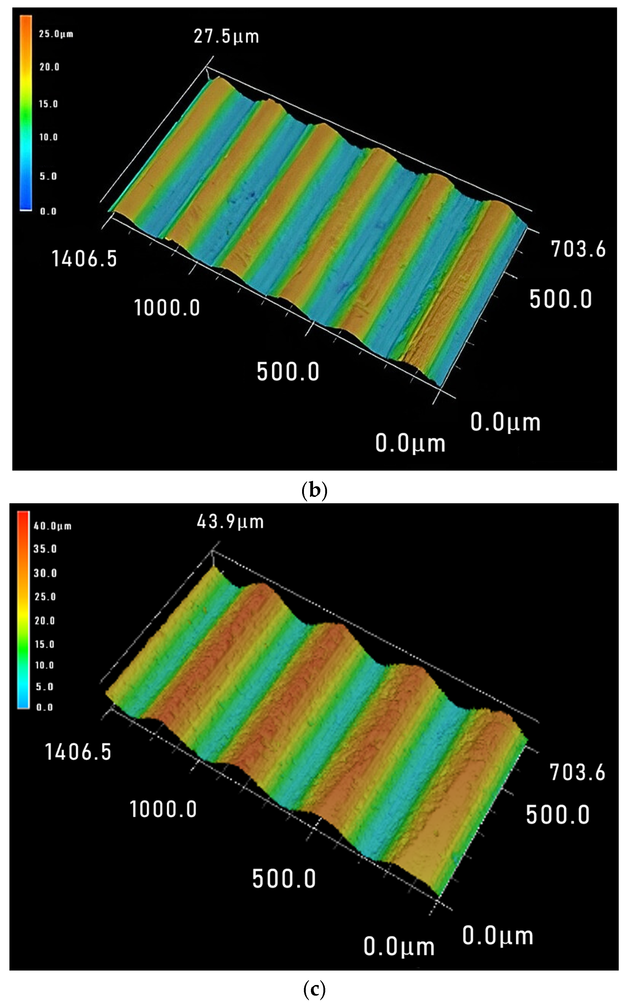
3.1. Effect of Process Parameters on Surface Roughness

Table 4 presents the average surface roughness values of NdFeB slices under 25 different parameter combinations. Compared with the sawing experiment results of Liu et al. [23], when using the same workpiece feed rate, the surface roughness value obtained in our sawing experiment decreased. The main reason is that the increase in wire speed leads to an increase in the number of abrasives entering the cutting zone per unit time.
Table 5 presents the range analysis results of surface roughness Ra. It can be observed that the range R values for feed rate, wire speed, and sawed workpiece size are 3.00, 1.51, and 0.79, respectively. This indicates that the feed rate has the greatest influence on surface roughness Ra, while the workpiece size has the least influence. Therefore, the order of influence on surface roughness Ra is feed rate (Vw) > wire speed (Vs) > sawed workpiece size (L). Figure 4 shows the mean values of the factors affecting surface roughness Ra. It can be seen more intuitively that the decrease in feed rate and workpiece size, as well as the increase in wire speed, are beneficial for improving surface roughness.
From the range analysis results of the orthogonal experiment, it is evident that the feed rate has a significant impact on the surface roughness Ra. Specifically, a higher feed rate results in a larger Ra value, and the minimum Ra value is achieved when the feed rate is 0.1 mm·min−1. The wire speed also influences Ra value, with an increase in wire speed leading to a reduction in Ra value. The minimum Ra value is observed at a wire speed of 1600 m·min−1. The workpiece size has the least effect on Ra, and a smaller workpiece size corresponds to a lower Ra value. The minimum Ra value is obtained when the sawed workpiece size is 10 mm. Based on the above analysis, the optimal experimental parameter combination for minimizing surface roughness Ra is A1B5C1. At this time, the workpiece feed rate is 0.1 mm·min−1, the wire speed is 1600 m·min−1, and the workpiece size is 10 mm.

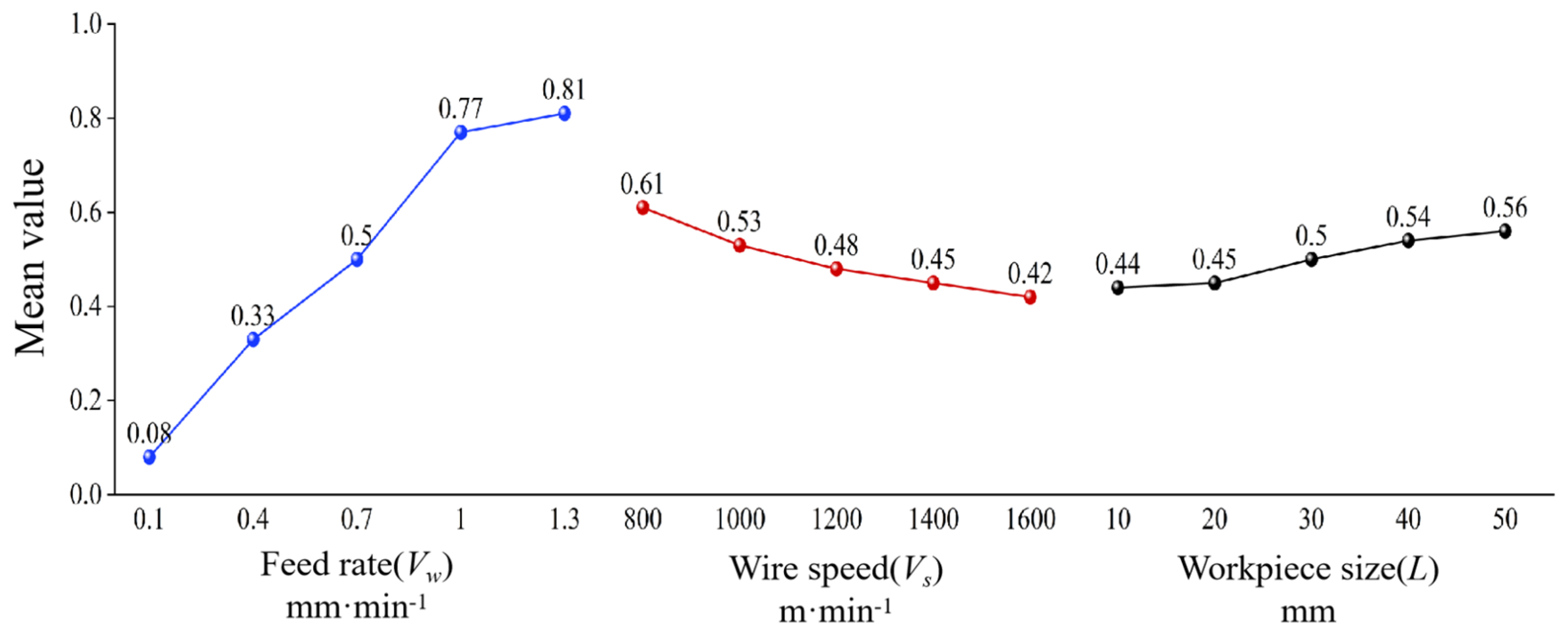
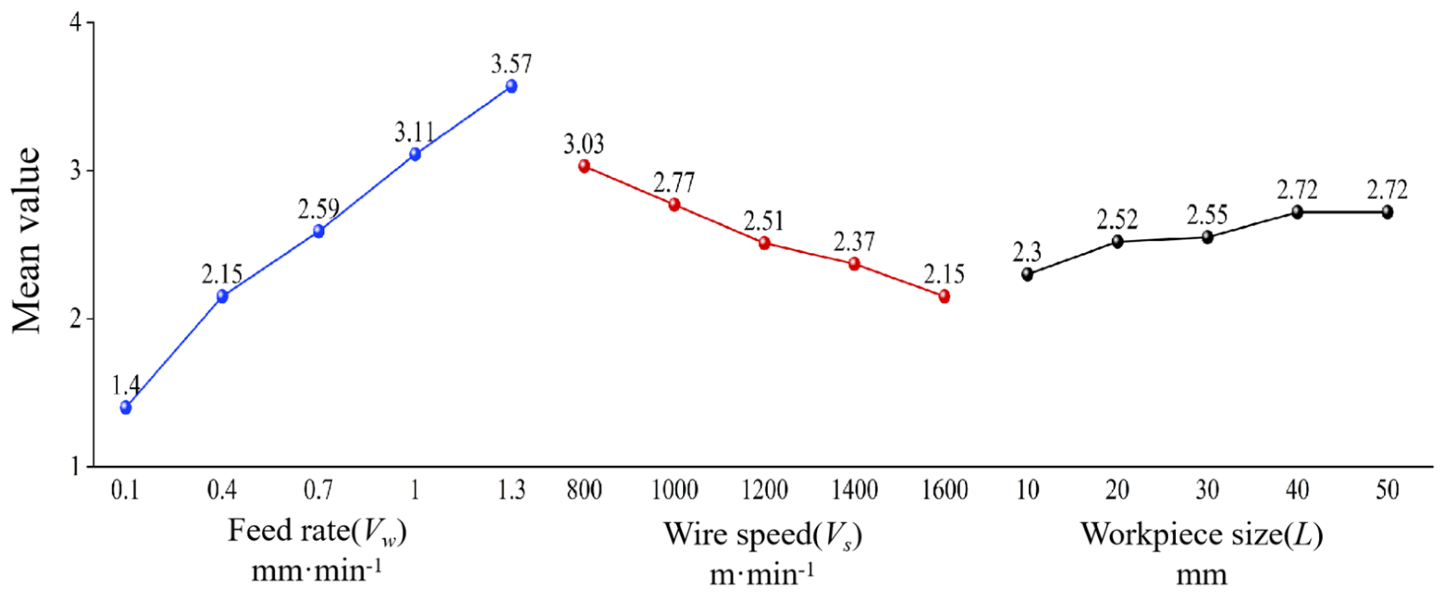
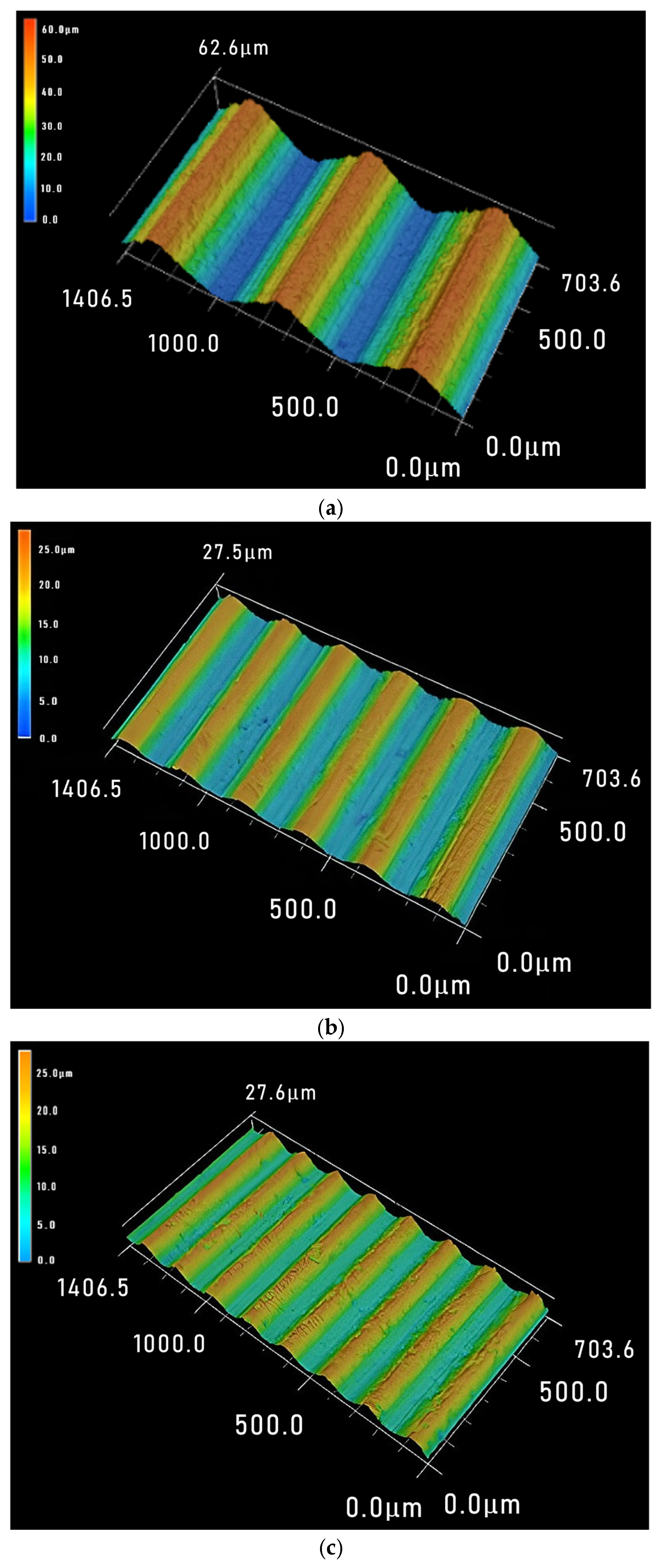
3.2. Effect of Process Parameters on Surface Waviness

The surface waviness Wa values of NdFeB slices under 25 groups of parameters were measured, as shown in Table 6. And Table 7 shows the range analysis results of the waviness Wa. The range R values of the workpiece feed rate, saw wire speed, and sawed workpiece size on the surface waviness Wa are 0.73, 0.2 and 0.12, respectively. It can be seen that the workpiece feed rate has the greatest impact on Wa, while the sawed workpiece size has the smallest impact. The order of the impact on Wa is as follows: workpiece feed rate (Vw) > wire speed (Vs) > workpiece size (L).
As shown in Figure 5, the average levels of various influencing factors on the waviness can be visually observed, which is that the decrease in feed rate and workpiece size, as well as the increase in wire speed, are beneficial for improving surface waviness. It can be concluded that the optimal process parameter combination for obtaining minimum surface waviness Wa is A1B5C1. Correspondingly, the workpiece feed rate is 0.1 mm·min−1, the sawing wire speed is 1600 m·min−1, and the sawed workpiece size is 10 mm.
The existence of periodic waviness on the processed surface significantly reduces the flatness and surface quality of the slices. In the previous content, the variation law of waviness Wa with processing parameters was explained. Here, further quantitative analysis is carried out by observing the peak valley difference (i.e., PV value) of the waviness contour curve to clarify the influence of feed rate, wire speed, and sawed workpiece size on PV value. The PV values of the sliced surfaces under various parameter combinations in the orthogonal experiment are shown in Table 8. Compared with the sawing experiment results of Liu et al. [23] and Wu et al. [24], the PV values of the sliced surface obtained in our sawing experiment decreased. The main reason for the analysis may be that the precision of the high-wire speed cutting equipment we use is higher than that of the low-wire speed sawing machine.
Table 9 shows the analysis results of the range of PV values on the sawed surface of NdFeB. According to the data in Table 9, the range R values of PV values for workpiece feed rate, wire speed, and workpiece size are 14.2, 8.7, and 4.22, respectively. It can be seen that the influence of workpiece feed rate on PV value is the greatest, while the influence of sawed workpiece size is the smallest. The order of the influence on PV value is obtained as workpiece feed rate (Vw) > wire speed (Vs) > sawed workpiece size (L). Based on the experimental analysis results shown in Table 9, it can be concluded that the optimal combination of experimental levels for obtaining minimum PV value is A1B5C1, which is consistent with the optimal experimental level derived from the analysis of Wa. Correspondingly, the workpiece feed rate is 0.1 mm·min−1, the saw wire speed is 1600 m·min−1, and the sawed workpiece size is 10 mm. Figure 6 shows the average levels of various influencing factors on PV value. The analysis results indicate that the decrease in feed rate and workpiece size, as well as the increase in wire speed are beneficial for decreasing the PV values.
In order to more intuitively show the periodic changes in surface waviness, a larger range of three-dimensional images of sliced surfaces was observed. Figure 7 shows the sawed 3D surface image when using a wire speed of 1200 m·min−1, and the periodic waviness can be clearly seen. It can be observed that the sawed workpiece size has almost no effect on the waviness period Tw of the sawed surface, while the larger the feed rate, the larger the period value Tw, which is consistent with the research conclusion of Liu et al. [23]. For the PV value, although the sawed workpiece size decreases sequentially from Figure 7a–c, the increase in feed rate has a greater impact on the PV value, so the waviness PV values show an increasing trend from Figure 7a–c.
Figure 8 shows the surface 3D morphology under three different process parameters with a feed rate of 1.0 mm·min−1. From Figure 8a–c, the workpiece size decreases continuously, and the wire speed gradually increases. It can be seen that the PV value gradually decreases from Figure 8a–c, indicating that the effect will not conflict when both parameter values change simultaneously and have the same impact on the surface. For the waviness period Tw, sawed workpiece size has almost no effect on it. And as the wire speed increases, the time it takes for the saw wire to run back and forth for one cycle decreases, so the feed distance decreases and the period Tw decreases.
Figure 9 shows the 3D surface morphology of three different process parameters with a sawed workpiece size of 50 mm. From Figure 9a–c, the feed rate and wire speed have both increased, and an increase in PV value can be observed. It can be seen that within the range of process parameters used in this paper, it is feasible to offset the negative impact of excessive feed rate on the sawed surface by increasing the wire speed. The waviness period Tw is also influenced by the combined effect of feed rate and wire speed, which means it needs to be determined based on specific values.
The PV value of surface waviness has a more significant impact on subsequent grinding processes, so it is necessary to develop a regression equation for PV to achieve its prediction by establishing a mapping relationship between process parameters and PV values. In the orthogonal experimental design of this paper, the five level values of each of the three factors are equally spaced. Therefore, it is suitable to use polynomial regression analysis to obtain the regression equation. By conducting regression analysis on the processing parameters and PV values used in the orthogonal experiment of this paper, the mathematical theoretical model for PV values can be obtained by using the MATLAB Version 2020 (Natick, MA, USA) as follows:
PV = 0.747 × Vs−0.342 × Vw0.546 × L0.109
From the above Equation (2), it can be seen that when the feed rate and sawed workpiece size increase and the wire speed decreases, the PV value will increase. And the absolute value of the exponent of Vw is the largest, followed by Vs, and L is the smallest. This indicates that feed rate has the most significant impact on PV value, while the sawed workpiece size has the least impact on PV value, which is consistent with the previous discussion.

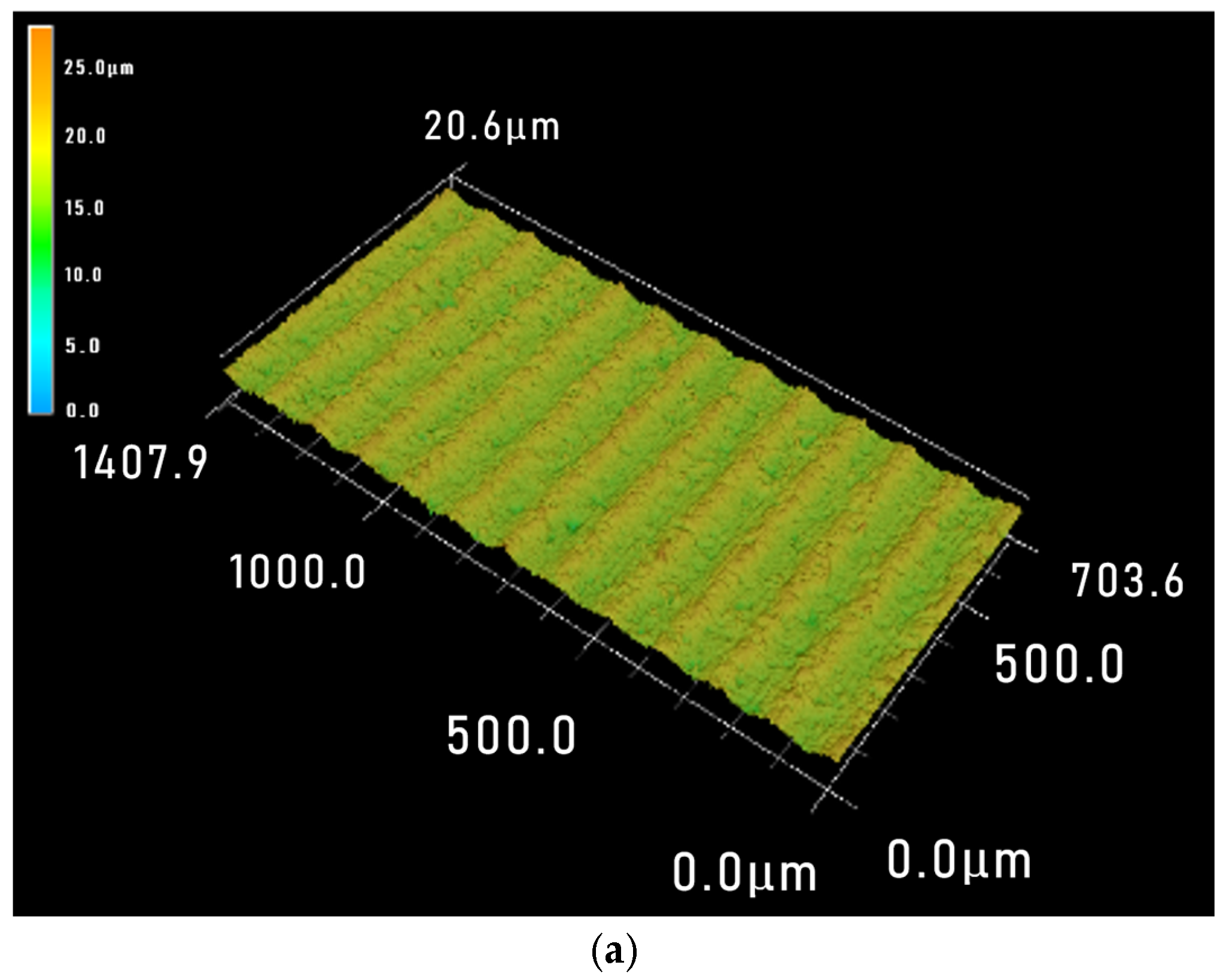
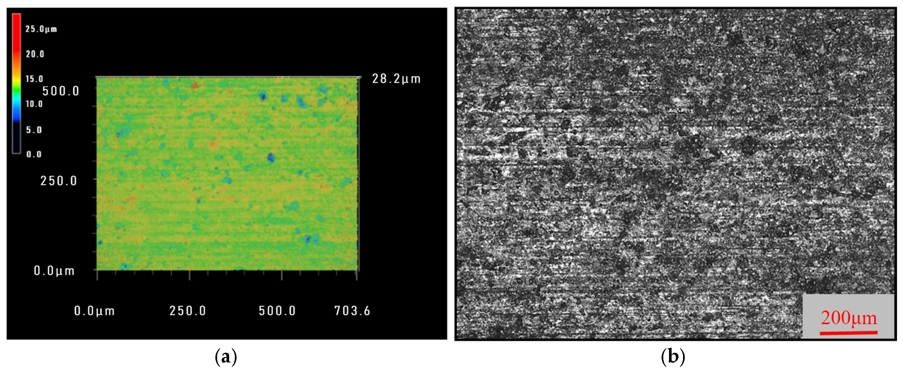
3.3. Sawing Results by Using Optimal Process Parameter Combination

The optimal process parameter combination predicted based on roughness Ra and waviness Wa is consistent, with a workpiece feed rate of 0.1 mm·min−1, a wire speed of 1600 m·min−1 and workpiece size of 10 mm. This parameter combination did not appear in the orthogonal experiment, so sawing experiments were conducted by using this parameter combination to verify the analysis correctness. The 3D and 2D images of the sawed surface morphology under this set of process parameters are shown in Figure 10. It can be seen that the processed surface is relatively smooth and flat. The roughness Ra and waviness Wa were measured at any five positions and their mean values were taken. The surface roughness Ra was 0.433 μm and the waviness Wa was 0.037 μm. The obtained Ra and Wa are both lower than the values under other processing parameters in the orthogonal experiment, which is consistent with the analysis results and proves the rationality of the conclusion.

4. Conclusions

This paper conducted a three-factor and five-level orthogonal experiment on diamond wire saw cutting NdFeB magnetic materials. The surface roughness Ra and waviness Wa were used as evaluation indicators to explore the influence of workpiece feed rate, wire speed and workpiece size on the sawed NdFeB surface characteristics. The PV value of the sawed surface waviness profile curve was further analyzed. The main conclusions obtained are as follows:
(1)
The sawing process parameters show a consistent trend in their impact on surface roughness Ra and waviness Wa. The decrease in workpiece feed rate and size, as well as the increase in wire speed, are beneficial for improving surface roughness and waviness. The order of the influence of various processing parameters on surface roughness Ra and waviness Wa is workpiece feed rate, wire speed, and workpiece size, and the influence of process parameters on the waviness PV value also shows a consistent trend.
(2)
The optimal combination of process parameters based on minimum Ra and Wa is consistent, which is that workpiece feed rate is 0.1 mm·min−1, wire speed is 1600 m·min−1, and workpiece size is 10 mm. Correspondingly, Ra is 0.433 μm and Wa is 0.037 μm. The regression equation for PV values established based on experimental data are PV = 0.747 × Vs−0.342 × Vw0.546 × L0.109.
The research results have clarified the order of the influence of process parameters on the quality of cutting NdFeB by diamond wire saw, and provided optimized parameter combinations, which provides an experimental basis and guidance for the sawing process. However, further exploration is needed to determine the impact of the interaction between multiple process parameters on the cut NdFeB surface properties during wire sawing, in order to achieve more precise optimization of process parameter combinations.

Author Contributions

C.P.: investigate, writing—original draft preparation, data curation. G.L.: writing—review and editing, methodology. X.Z.: investigate, methodology, writing—original draft preparation. Y.G.: writing—review and editing, project administration, funding acquisition. All authors have read and agreed to the published version of the manuscript.

Funding

The work is financially supported by Natural Science Foundation of Shandong Province (No. ZR2023ME145).

Institutional Review Board Statement

Not applicable.

Informed Consent Statement

Not applicable.

Data Availability Statement

The original contributions presented in this study are included in the article. Further inquiries can be directed to the corresponding author.

Conflicts of Interest

The authors declare no conflicts of interest.

References

  1. Wang, Z.; Chang, S.; Bao, X.; Yu, H.; Guan, S.; Zhu, K.; Zheng, Y.; Li, J.; Gao, X. Interpretable Prediction of Remanence in Sintered NdFeB through Machine Learning Strategy. J. Alloys Compd. 2024, 1008, 176727. [Google Scholar] [CrossRef]
  2. Yang, Y.; Jiang, N.; Sun, Y.; Yang, L.; Guan, C.; Zhang, E.; Fanf, X.; Liu, J. Structure and Corrosion Resistance Characteristics of ZnAl/EP Coating on Bonded NdFeB Magnet. J. Mater. Eng. Perform. 2023, 32, 5475–5482. [Google Scholar] [CrossRef]
  3. Yang, T.; Zhu, X.; Zhao, W.; Zhao, Q.; Liu, G. Low Temperature Machining Advantages for Sintered NdFeB Magnets: A Comparative Experimental Study of WAWJ with Laser and WEDM. J. Mater. Eng. Perform. 2024, 610, 172589. [Google Scholar] [CrossRef]
  4. Greer, J.; Petruska, A.; Mahoney, A.; Nambi, M.; Bamberg, E.; Abbott, J. Experimental Investigation of Wire Electrical Discharge Machining of NdFeB Permanent Magnets with an RC-Type Machine. J. Mater. Eng. Perform. 2014, 23, 1392–1401. [Google Scholar] [CrossRef]
  5. Wang, C.; Lian, Z.; Yu, P.; Xu, J. Experimental Study on Magnetic Field Assisted WEDM Machining Sintered NdFeB. Mach. Des. Manuf. 2022, 10, 32–40. [Google Scholar] [CrossRef]
  6. Ma, X.; Teng, K. Research on High Efficiency and Low Loss Cutting of NdFeB Permanent Magnet Material by WEDM. Manuf. Technol. Mach. Tool. 2017, 4, 97–101. [Google Scholar]
  7. Wang, L.; Zhang, J.; Xu, Y.; Han, W.; Zhou, L. Effect of Fiber Laser Cutting Technology on Sintered NdFeB Magnetic Performance. Met. Funct. Mater. 2023, 30, 80–86. [Google Scholar] [CrossRef]
  8. Ren, N.; Liu, G.; Li, X.; Tong, Z. Simulation Analysis of Temperature Field of Laser Cut Ndfeb Magnetic Material. Manuf. Technol. Mach. Tool 2020, 1, 25–29. [Google Scholar] [CrossRef]
  9. Ma, C.; Liu, G.; Li, X.; Ding, L. Study on the Effect of Sintered NdFeB Laser Cutting Quality Technology. Manuf. Technol. Mach. Tool 2019, 3, 113–117. [Google Scholar] [CrossRef]
  10. Yao, C.; Yu, X.; Feng, L.; Wang, F.; Wang, F.; Yuan, Q. Development of Microencapsulated Phase Change Material Slurry for Diamond Wire Sawing Silicon Wafer and Its Effect on Cutting Quality. J. Manuf. Process. 2024, 127, 421–432. [Google Scholar] [CrossRef]
  11. Qiu, J.; Li, X.; Ge, R.; Wu, R.; Liu, C. Surface Formation, Morphology, Integrity and Wire Marks in Diamond Wire Slicing of Mono-Crystalline Silicon in the Photovoltaic Industry. Wear 2022, 488–489, 204186. [Google Scholar] [CrossRef]
  12. Wang, J.; Li, S.; Liang, L.; Hao, Z.; Liu, F.; Landers, R. Cutting Force Modeling and Control of Single Crystal Silicon using Wire Saw Velocity Reciprocation. Proc. Inst. Mech. Eng. B-J. Eng. Manuf. 2024, 238, 823–836. [Google Scholar] [CrossRef]
  13. Ban, X.; Li, Y.; Han, S.; Qiu, H.; Wang, X.; Cui, Z. Parameters optimization for ferrite slicing based on grey theory. Diam. Abras. Eng. 2022, 42, 332–337. [Google Scholar] [CrossRef]
  14. Sefene, E.; Chen, C.; Yang, J. Sustainable Assessment of Diamond Wire Sawing for Monocrystalline Silicon Wafers: Conventional and Electrophoretic Cooling strategies. Manuf. Lett. 2025, 43, 46–50. [Google Scholar] [CrossRef]
  15. Costa, E.; Bellen, B.; Werner, M.; Sousa, P.; Xavier, F. Optimizing the Diamond Wire Sawing of Polycrystalline Silicon: An Experimental Approach. Mater. Sci. Semicond. Proc. 2024, 185, 108938. [Google Scholar] [CrossRef]
  16. Zhu, Z.; Gao, Y.; Zhang, X. Study on Subsurface Microcrack Damage Depth of Diamond Wire as-Sawn Sapphire Crystal Wafers. Eng. Fract. Mech. 2023, 28, 109347. [Google Scholar] [CrossRef]
  17. Liu, Y.; Huang, H.; Wang, L.; Liao, X. Experimental Study on Normal Force of Cutting Sapphire with Multi-Wire Swing Reciprocating Wire Saw. Diam. Abras. Eng. 2024, 44, 143–150. [Google Scholar] [CrossRef]
  18. Yang, H.; Fu, M.; Zhang, X.; Zhu, K.; Cao, L.; Hu, C. Material Removal Mechanisms of Polycrystalline Silicon Carbide Ceramic Cut by a Diamond Wire Saw. Materials 2024, 17, 4238. [Google Scholar] [CrossRef]
  19. Chen, Y.; Zhang, S.; Zhang, X.; Yuchi, G.; Duan, J.; Jiang, R.; Zhou, Y. Study on Mechanism and Process of Cutting Silicon Carbide Ceramics with Diamond Wire Saw. Diam. Abras. Eng. 2021, 41, 60–67. [Google Scholar] [CrossRef]
  20. Seeholzer, L.; Süssmaier, S.; Kneubühler, F.; Wegener, K. Experimental Investigation of The Machining Characteristics in Diamond Wire Sawing of Unidirectional CFRP. Int. J. Adv. Manuf. Technol. 2021, 117, 2197–2212. [Google Scholar] [CrossRef]
  21. Magdalena, W.; Mateusz, P.; Christian, G.; Dariusz, P. Investigation of Abrasive Cutting of Ceramic Matrix Composites Based on Thin-Walled Elements using Diamond Wire. Tehnički Vjesnik 2022, 29, 641–645. [Google Scholar] [CrossRef]
  22. Liu, Y.; Gao, Y.; Li, G.; Shi, Z. Influences of Fiber Orientation and Process Parameters on Diamond Wire Sawn Surface Characteristics of 2.5D Cf/SiC Composites. Mater. Today Commun. 2024, 41, 110421. [Google Scholar] [CrossRef]
  23. Liu, J.; Zhang, Z.; Wan, S.; Wu, B.; Feng, J.; Zhang, T.; Zhou, C. Experimental and Theoretical Investigations on Diamond Wire Sawing for a NdFeb Magnet. Materials 2022, 15, 3034. [Google Scholar] [CrossRef] [PubMed]
  24. Wu, B.; Zhang, Z.; Feng, J.; Meng, F.; Wan, S.; Zhuang, X.; Li, L.; Liu, H.; Zhang, F. Experimental Investigation on the Surface Formation Mechanism of Ndfeb During Diamond Wire Sawing. Materials 2023, 16, 1521. [Google Scholar] [CrossRef]
  25. Zhang, X.; Gao, Y.; Yang, C.; Shi, Z. Surface Characteristics of Precision As-Cut NdFeB Magnet Considering Diamond Wire Wear. Precis. Eng. 2024, 89, 23–36. [Google Scholar] [CrossRef]
  26. Costa, E.; Lima, A.; Santos, M.; Souza, R.; Wendhausen, P.; Xavier, F. On the Mechanical Behavior of the Sintered Nd-Fe-B Permanent Magnet during Diamond Scratching. J. Manuf. Process. 2023, 94, 79–93. [Google Scholar] [CrossRef]
  27. Sopori, B.; Basnyat, P.; Devayajanam, S.; Schnepf, R.; Sahoo, S.; Gee, J.; Severico, F.; Manens, A.; Seigneur, H.; Scjoenfeld, W. Analyses of Diamond Wire Sawn Wafers: Effect of Various Cutting Parameters. In Proceedings of the IEEE 42nd Photovoltaic Specialist Conference, New Orleans, LA, USA, 14–19 June 2015. [Google Scholar] [CrossRef]
  28. Gupta, A.; Chen, C.; Hsu, H. Study on Diamond Wire Wear, Surface Quality, and Subsurface Damage during Multi-Wire Slicing of C-Plane Sapphire Wafer. Int. J. Adv. Manuf. Technol. 2019, 100, 1801–1814. [Google Scholar] [CrossRef]
  29. Costa, E.; Weingaertner, W.; Xavier, F. Influence of Single Diamond Wire Sawing of Photovoltaic Monocrystalline Silicon on the Feed Force, Surface Roughness and Micro-crack Depth. Mater. Sci. Semicond. Proc. 2022, 143, 106525. [Google Scholar] [CrossRef]
  30. Wang, J.; Li, S.; Liang, L. Experiment Comparative Analysis of Feed Rate with Velocity Control in Cutting Mono Crystalline Silicon Using a Diamond Wire Saw. Micromachines 2024, 15, 473. [Google Scholar] [CrossRef]
  31. Guo, Y.; Gao, Y.; Yang, C. Sawing Force Modeling and Analysis for Diamond Wire Sawing PV Monocrystalline Silicon Considering Abrasive Wear. Wear 2025, 562–563, 205669. [Google Scholar] [CrossRef]
  32. Guo, Y.; Gao, Y.; Zhang, X.; Shi, Z. Wire Bow Analysis Based on Process Parameters in Diamond Wire Sawing. Int. J. Adv. Manuf. Technol. 2024, 131, 2909–2924. [Google Scholar] [CrossRef]
  33. Yin, Y.; Gao, Y.; Li, X.; Pu, T.; Wang, L. Experimental Study on Slicing Photovoltaic Polycrystalline Silicon with Diamond Wire Saw. Mater. Sci. Semicond. Proc. 2020, 106, 104779. [Google Scholar] [CrossRef]
  34. Liedke, T.; Kuna, M. A Macroscopic Mechanical Model of the Wire Sawing Process. Int. J. Mach. Tools Manuf. 2011, 51, 711–720. [Google Scholar] [CrossRef]
  35. Lai, Z.; Liao, X.; Yang, H.; Hu, Z.; Huang, H. Experimental Study on the Formation Mechanism of Saw Marks in Wire Sawing. Int. J. Mech. Sci. 2024, 265, 108894. [Google Scholar] [CrossRef]
  36. Louise, C.; Roland, R.; Daniel, N.; Marion, F.; Fabrice, C.; Ainal, C. Comparative Analysis of Mechanical Strength of Diamond-Sawn Silicon Wafers Depending on Saw Mark Orientation, Crystalline Nature and Thickness. Sol. Energy Mater. Sol. Cells 2019, 201, 110068. [Google Scholar] [CrossRef]
  37. Jung, I.; Song, S.; Choi, M.; Yu, H.; Kim, S. Evolution of Mechanically Formed Bow Due to Surface Waviness and Residual Stress Difference on Sapphire (0001) Substrate. J. Mater. Process. Technol. 2019, 269, 102–108. [Google Scholar] [CrossRef]
  38. Teomete, E. Investigation of Long Waviness Induced by the Wire Saw Process. Proc. Inst. Mech. Eng. Part B J. Eng. Manuf. 2011, 225, 1153–1162. [Google Scholar] [CrossRef]
  39. Li, G.; Gao, Y.; Huang, W.; Shi, Z. Improvement of Wire Marks on the Surface of Si3N4 Ceramics Cut by Diamond Wire Saw. Mater. Sci. Eng. B-Adv. 2024, 310, 117725. [Google Scholar] [CrossRef]
  40. Wen, B. Mechanical Design Manual, 6th ed.; China Machine Press: Beijing, China, 1997. [Google Scholar]
Figure 1. Different processing steps for sintered NdFeB magnet, (a) powdered raw materials, (b) sintered raw blocks, (c) sliced, (d) electroplated finished products.
Materials 18 01173 g001
Figure 2. Experimental flow diagram. (a) Schematic of the wire saw machine; (b) magnified view of the machining process; (c) schematic of the slice dimensions;(d) NdFeB slices.
Materials 18 01173 g002
Figure 3. Three-dimensional and two-dimensional surface topography of the slice and its data measurement diagram (a) cross-section profile curve, (b) surface roughness profile curve, and (c) waviness profile curve.
Materials 18 01173 g003
Figure 4. Mean levels of various influencing factors on roughness Ra.
Materials 18 01173 g004
Figure 5. Mean levels of various influencing factors on waviness Wa.
Materials 18 01173 g005
Figure 6. Mean levels of various influencing factors on PV value.
Materials 18 01173 g006
Figure 7. Three sets of slice 3D morphology under the condition of wire speed = 1200 m·min−1 (Vw-L). (a) 0.4 mm·min−1-40 mm; (b) 1.0 mm·min−1-20 mm; (c) 1.3 mm·min−1-10 mm.
Materials 18 01173 g007aMaterials 18 01173 g007b
Figure 8. Three sets of slice 3D morphology under the condition of feed rate vw = 1.0 mm·min−1 (Vs-L). (a) 800 m·min−1n-30 mm; (b) 1200 m·min−1-20 mm; (c) 1600 m·min−1-10 mm.
Materials 18 01173 g008
Figure 9. Three sets of slice 3D morphology under the condition of workpiece size L = 50 mm (Vw-Vs). (a) 0.4 mm·min−1-800 m·min−1; (b) 1.0 mm·min−1-1000 m·min−1; (c) 1.3 mm·min−1-1600 m·min−1.
Materials 18 01173 g009
Figure 10. Three-dimensional (a) and two-dimensional (b) surface topographies under optimal processing parameter combinations: Vw = 0.1 m·min−1, Vs = 1600 m·min−1, and L = 10 mm.
Materials 18 01173 g010
Table 1. Parameters of diamond wire.
ParametersValues
Diamond saw wire length (m)70
Diameter of saw wire core (μm)220
Type of abrasivesNickel-coated diamond
Abrasive size (μm)70–85
Abrasive distribution density (grits·mm−1)15–20
Tensile limit of saw wire (MPa)3275
Moh’s hardness of saw wire (nickel plating)5
Table 2. Factors and levels of the orthogonal experiment.
LevelsFactors
(A) Feed Rate (Vw)
/mm·min−1
(B) Wire Speed (Vs)
/m·min−1
(C) Workpiece Size (L)
/mm
10.1 (A1)800 (B1)10 (C1)
20.4 (A2)1000 (B2)20 (C2)
30.7 (A3)1200 (B3)30 (C3)
41.0 (A4)1400 (B4)40 (C4)
51.3 (A5)1600 (B5)50 (C5)
Table 3. Experimental parameter combinations.
No.Parameter CombinationsNo.Parameter Combinations
1 A 1 B 1 C 1 14 A 3 B 4 C 5
2 A 1 B 2 C 3 15 A 3 B 5 C 2
3 A 1 B 3 C 5 16 A 4 B 1 C 3
4 A 1 B 4 C 2 17 A 4 B 2 C 5
5 A 1 B 5 C 4 18 A 4 B 3 C 2
6 A 2 B 1 C 5 19 A 4 B 4 C 4
7 A 2 B 2 C 2 20 A 4 B 5 C 1
8 A 2 B 3 C 4 21 A 5 B 1 C 2
9 A 1 B 4 C 1 22 A 5 B 2 C 4
10 A 2 B 5 C 3 23 A 5 B 3 C 1
11 A 3 B 1 C 4 24 A 5 B 4 C 3
12 A 3 B 2 C 1 25 A 5 B 5 C 5
13 A 3 B 3 C 3
Table 4. Surface roughness Ra values of NdFeB slices.
No.Ra (μm)No.Ra (μm)No.Ra (μm)
10.634101.129192.501
20.679113.489201.720
30.732122.247214.847
40.522132.051224.319
50.579142.239232.979
62.382151.512242.732
71.281164.416253.263
81.387173.875
90.964182.378
Table 5. Range analysis of surface roughness Ra.
ParametersLevelsK ValuesKavg ValuesOptimal LevelRange R Value
A A 1 3.150.63 A 1 3.00
A 2 7.141.43
A 3 11.542.31
A 4 14.892.98
A 5 18.143.63
B B 1 15.773.15 B 5 1.51
B 2 12.402.48
B 3 9.531.91
B 4 8.961.79
B 5 8.201.64
C C 1 8.541.71 C 1 0.79
C 2 10.542.11
C 3 11.012.20
C 4 12.272.45
C 5 12.492.50
Table 6. Surface waviness Wa values of NdFeB slices.
No.Wa (μm)No.Wa (μm)No.Wa (μm)
10.083100.244190.709
20.085110.713200.645
30.086120.489210.866
40.069130.497220.879
50.074140.475230.756
60.513150.327240.767
70.303160.897250.803
80.346170.913
90.237180.695
Table 7. Range analysis of surface waviness Wa.
ParametersLevelsK ValuesKavg ValuesOptimal LevelRange R Value
A A 1 0.400.08 A 1 0.73
A 2 1.640.33
A 3 2.500.50
A 4 3.860.77
A 5 4.070.81
B B 1 3.070.61 B 5 0.2
B 2 2.670.53
B 3 2.380.48
B 4 2.260.45
B 5 2.090.42
C C 1 2.210.44 C 1 0.12
C 2 2.260.45
C 3 2.490.50
C 4 2.720.54
C 5 2.790.56
Table 8. PV values of NdFeB slices in orthogonal experiment.
No.PV (μm)No.PV (μm)No.PV (μm)
11.415101.789192.916
21.425111.802202.317
31.432123.271214.024
41.345132.631223.885
51.375142.553233.373
62.785152.005243.315
72.217163.633253.243
82.149173.673
91.789183.021
Table 9. Range analysis of PV values.
ParametersLevelsK ValuesKavg ValuesOptimal LevelRange R Value
A A 1 6.991.40 A 1 2.17
A 2 10.742.15
A 3 12.942.59
A 4 15.563.11
A 5 17.843.57
B B 1 15.133.03 B 5 0.88
B 2 13.832.77
B 3 12.532.51
B 4 11.842.37
B 5 10.742.15
C C 1 11.522.30 C 1 0.42
C 2 12.612.52
C 3 12.732.55
C 4 13.602.72
C 5 13.612.72
Disclaimer/Publisher’s Note: The statements, opinions and data contained in all publications are solely those of the individual author(s) and contributor(s) and not of MDPI and/or the editor(s). MDPI and/or the editor(s) disclaim responsibility for any injury to people or property resulting from any ideas, methods, instructions or products referred to in the content.

