Article

The Effect of B2O3 Doping on the Properties of Electrical and Thermal Conductivity for SnO2 Varistors

The Wind Solar Storage Division, State Key Laboratory of Control and Simulation of Power System and Generation Equipment, School of Electrical Engineering, Xinjiang University, Urumqi 830046, China
*
Author to whom correspondence should be addressed.
Materials 2025, 18(7), 1399; https://doi.org/10.3390/ma18071399
Submission received: 21 February 2025 / Revised: 13 March 2025 / Accepted: 19 March 2025 / Published: 21 March 2025

Abstract

:
This study investigates SnO2-based varistors in the SnO2-Co3O4-Cr2O3-Nb2O5 system with varying B2O3 doping concentrations to optimize both electrical properties and thermal conductivity. The experimental formulation involved doping B2O3 with fixed concentration ratios of Co3O4, Cr2O3, and Nb2O5 (ranging from 0 mol% to 0.35 mol%), and the microstructure, electrical properties, and thermoelectric coefficient of the samples were measured in order to identify the optimal doping proportion. The varistor doped with 0.25 mol% B2O3 exhibited optimal performance, demonstrating a maximum voltage gradient of 525 V/mm, a minimum leakage current density of 11.2 μA/cm2, and a peak nonlinear coefficient of 36. Furthermore, the optimized formulation achieved enhanced thermal performance with a maximum thermal conductivity of 6.13 W·m−1·K−1.

1. Introduction

As the construction of ultra-high-voltage (UHV) power grid projects advanced gradually, the voltage levels and transmission capacities of these grids also increased progressively, which in turn led to a higher incidence of lightning-induced tripping. Statistics indicated that in China’s power system, more than 50% of the faults occurring annually were caused by lightning strikes, resulting in the tripping of transmission lines [1,2]. The installation of high-performance surge arresters had been proven to effectively suppress the overvoltage levels in power transmission systems within the limits that the insulation of the power equipment could withstand. This not only enhanced the insulation level of the power system but also simplified the insulation design of the power system, thereby reducing the manufacturing costs and technical difficulties associated with insulating equipment [3].
Currently, zinc oxide (ZnO) and tin oxide (SnO2) are the more commonly used metal oxides in surge arresters. Unlike the complex multiphase structure of ZnO varistors, SnO2 varistor ceramics possess a single-phase structure. Moreover, the additives in SnO2 varistor ceramics exhibit minimal volatilization during the sintering process, resulting in negligible doping losses due to volatilization. This characteristic endows SnO2 varistor ceramics with a more uniform microstructure. Consequently, the current flowing through its interior, as well as the corresponding temperature and thermal stress distributions, are more uniform under various operating conditions [4,5,6]. The thermal conductivity of SnO2 varistors at the same temperature is almost twice that of ZnO varistors. Compared with the latter, SnO2 varistors have better thermal conductivity and high-temperature resistance. Good thermal conductivity can quickly transfer the local temperature of the varistor, improving the safety and stability of the power system. Furthermore, SnO2-based piezoresistive ceramics exhibit distinct advantages including a simplified microstructure configuration and enhanced densification characteristics (relative density >98% TD) [7,8].
One study [9] demonstrated that SnO2 varistors with optimized grain boundary barrier characteristics can be fabricated through a segregation-induced and acceptor co-doping strategy, thereby achieving enhanced electrical nonlinearity with a nonlinear coefficient (α) of 36 ± 0.5. In the fabrication process of SnO2 varistors, the addition of a small amount of CoO/Co2O3, Nb2O5, and Cr2O3 can regulate the amplitude and width of the voltage barriers at the grain boundaries, thereby obtaining samples with different microstructures [10,11].
Another study [12] reported that SnO2 varistors containing 1.00 mol% CoO, 0.05 mol% Cr2O3, and 0.05 mol% Nb2O5 had a nonlinear coefficient of 41 and a voltage gradient of 400 V/mm. However, a rapid increase in the local temperature of the varistor can cause thermal collapse [13]. The doping of B2O3 in ZnO varistor formulations facilitates ionic exchange between ZnO grains and additive components at the grain boundaries, thereby effectively enhancing the barrier height ( φ b ) while reducing leakage currents [11].
Several studies have reported the use of different nanomaterials for varistors. For example, ZnO-based nanomaterials have been widely studied due to their excellent nonlinear electrical properties [13]. However, SnO2-based nanomaterials have gained attention because of their single-phase structure, minimal volatility of additives during sintering, and superior thermal conductivity compared to ZnO varistors. The performance of varistors can be significantly improved by tuning the nanomaterials. Adjusting the grain size, doping concentration, and microstructure can optimize the electrical and thermal properties. For instance, the formation of oxygen vacancies through doping can enhance the nonlinearity coefficient and conductivity [13,14,15].
In order to find a formulation with both good electrical properties and high thermal conductivity, this paper adds 0.05–0.35 mol% B2O3 to the doping system of SnO2-Co3O4-Cr2O3-Nb2O5 described in the literature [10,11,12,16]. Through experimental tests, it analyses the effect of different B2O3 doping amounts on the microstructure of SnO2 varistors and further explores the influence of the microstructure on both the electrical properties and thermal conductivity of SnO2 varistors. It also explores how to better improve the performance of piezoresistors by tuning the structure and properties of nanomaterials, e.g., by controlling microstructural factors such as grain size, porosity, and oxygen vacancy concentration.

2. Experimental

Samples of SnO2 with varied contents of B2O3-doped varistors were prepared based on the SnO2-Co3O4-Cr2O3-Nb2O5 system with the following raw materials: SnO2 (98.2% sample purity), Co3O4 (97.8% sample purity), Cr2O3 (97.9% sample purity), Nb2O5 (98.3% sample purity), and B2O3 (98.4% sample purity). The samples were prepared according to the following ratios (all molar fractions): (99.55-X) mol% SnO2, 0.05 mol% Co3O4, 0.05 mol% Cr2O3, 0.35 mol% Nb2O5, and Xmol% B2O3 (X = 0.05, 0.15, 0.25, 0.35) for raw material configuration. The specimen preparation process adopted the industrial standardized production process. The specific preparation process is as follows: To a certain proportion of SnO2 powder in a ball mill, the appropriate amount of deionized water was added for dispersion ball milling for 4 h. Then, the modified additives Co3O4, Cr2O3, Nb2O5, B2O3, and so on were added to the ball mill at the same time as an appropriate amount of deionized water, PVA (polyvinyl alcohol), and dispersant (sodium polyacrylate NaPAC), and ball milling continued for 4 h. The dispersed ball-milled mixed slurry was placed in the spray pelletizing tower for spray pelletizing.
The spray-granulated material was placed in a circular mold, and 380 MPa pressure was applied to press it into a circular billet with a diameter of 25 mm and a thickness of 2.5 mm. The pressed embryo was placed in a tunnel furnace, adhesive stripping was performed at a temperature of 650 °C for 8 h, and then it was transferred to a high-temperature furnace (NaberthermLH60/14). The sintering temperature was 1300 °C, the holding time was 3 h, and the heating rate was 5 °C/min. After natural cooling to room temperature, the desired SnO2 varistor sample was obtained. The upper and lower surfaces of the sintered cylindrical SnO2 varistor samples were polished, and then the surfaces were coated with silver electrodes and cured at 200 °C for 30 min to obtain the SnO2 varistor samples that were used for subsequent testing. The process flow diagram is shown in Figure 1.

3. Sample Testing

In order to study the electrical characteristics of SnO2 varistor samples, the electrical parameters and micromorphology were measured and observed. The microstructures of the sample sections were observed using a scanning electron microscope (Hitachi8010, Hitachi, Chiyoda, Japan), and the average grain size of the SnO2 varistor samples was obtained from the measured SEM (Scanning electron microscope) images using the intercept method, which is given by Equation (1) [13,14,15,17,18,19].
d = 1.56 L M N
In Equation (1), L is the length of the reference line measured in the SEM image; M is the magnification of the SEM photo; N is the number of SnO2 grains contained in the reference line.
SnO2 IV characteristics of the varistor samples were measured by a digital source meter (Model 2410, AprilAire, Madison, WI, USA), the value of the voltage gradient was the voltage across the varistor when 1 mA DC current flowed through the varistor, and the leakage current was the value of the current density corresponding to 0.75 V1 mA. The nonlinear coefficient α Equation (2) was used for calculations [20].
α = 1 log E 2 log E 1
In Equation (2), E 2 and E 1 are the voltage values at a current density of 1 mA/cm2 and 0.1 mA/cm2 flowing through the varistor, respectively.
The measurement of the CV characteristics of piezoresistive materials and the calculation of related data such as barrier height, donor density, and acceptor density involved a broadband dielectric spectrometer (Novocontrol Concept 80, Novocontrol, Montabaur, Germany) [21].
1 C b 1 2 C b 0 2 = 2 φ b + U g b q ε r ε 0 N d
In Equation (3), C b 0 is the capacitance per unit area without bias voltage; C b is the capacitance per unit area without bias voltage; U g b is the bias voltage on the single grain boundary; q is the electronic charge; ε r is the relative dielectric constant of the SnO2 varistor; N d is the donor density; φ b is the Schottky barrier height; φ b and N d are obtained from the intercept and slope of the CV curve.
The relationship between the barrier height φ b , the donor density N d , and the interfacial state density N i is shown in Equation (4), where ε 0 is the vacuum dielectric constant.
N i = 2 N d ε r ε 0 φ b q 1 2
In order to analyze the thermal behavior of the samples, the heat flux (Q) was measured using a DRL thermal conductivity meter (Xiangtan, China) based on the theory of the heat flow method [22]. The thermal conductivity coefficient K was calculated using Equation (5) [23]:
K = Q L A T
where the L is the thickness of the sample, the A is the area of the sample, and the T is the temperature difference between the cold and hot sides of the sample. The porosity P of the sample was measured by Archimedes method and calculated as [24]
P = ρ t h ρ p r ρ t h × 100 %
In Equation (6), ρ p r is the actual density, and ρ t h is the theoretical density [18].
The presence of defects such as point defects, grain boundaries, and dislocations affect the mean free range of phonons. The mean free path of a phonon can be described by the equation
1 l ω , T = 1 l i ω , T + 1 l p ω + 1 l b
l i ω , T is the phonon–phonon mean free range; l p ω is the mean free range reduced by scattering from point defects; l b is the mean free range reduced by grain boundary scattering [23].

4. Experimental Results
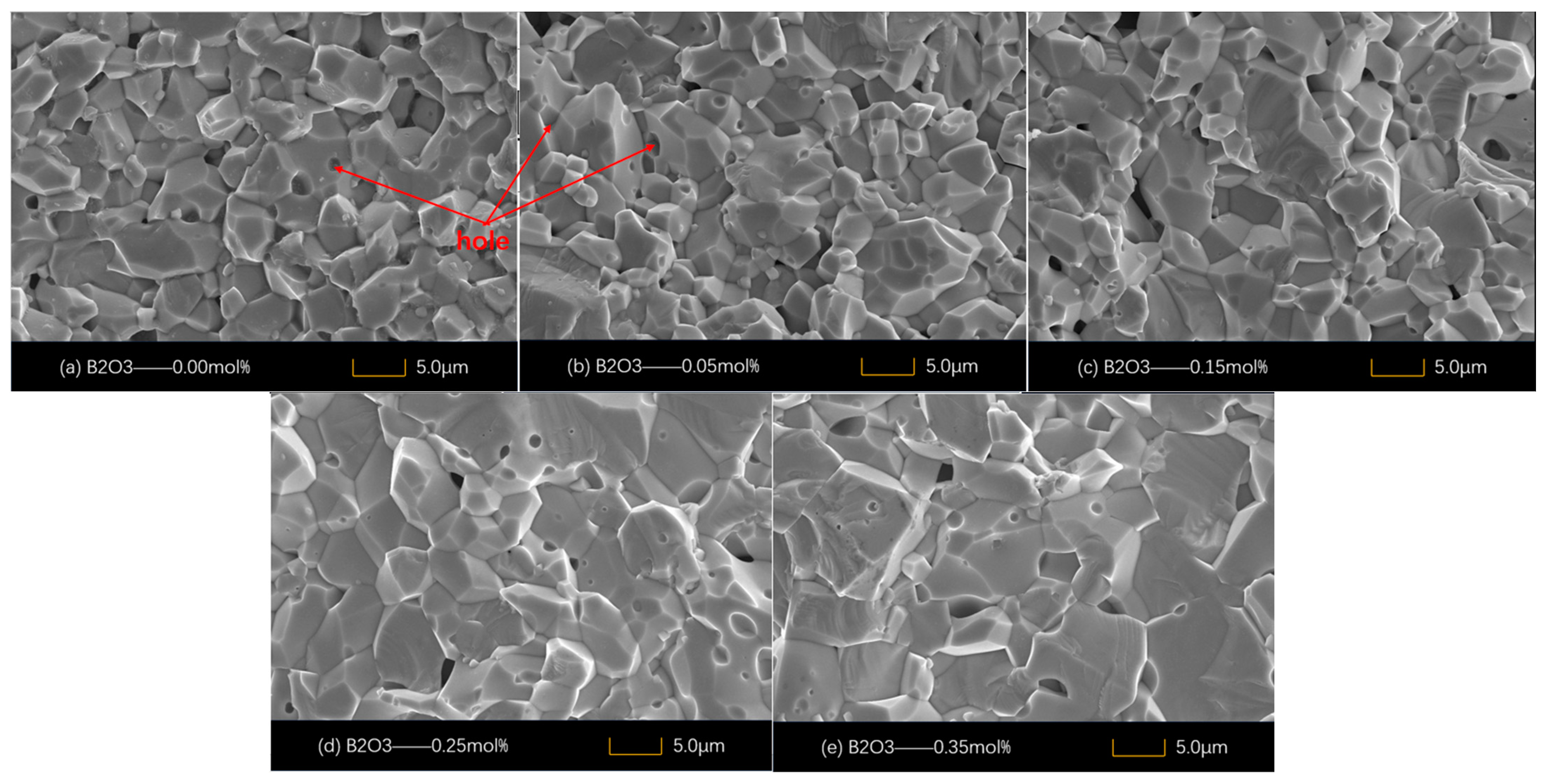
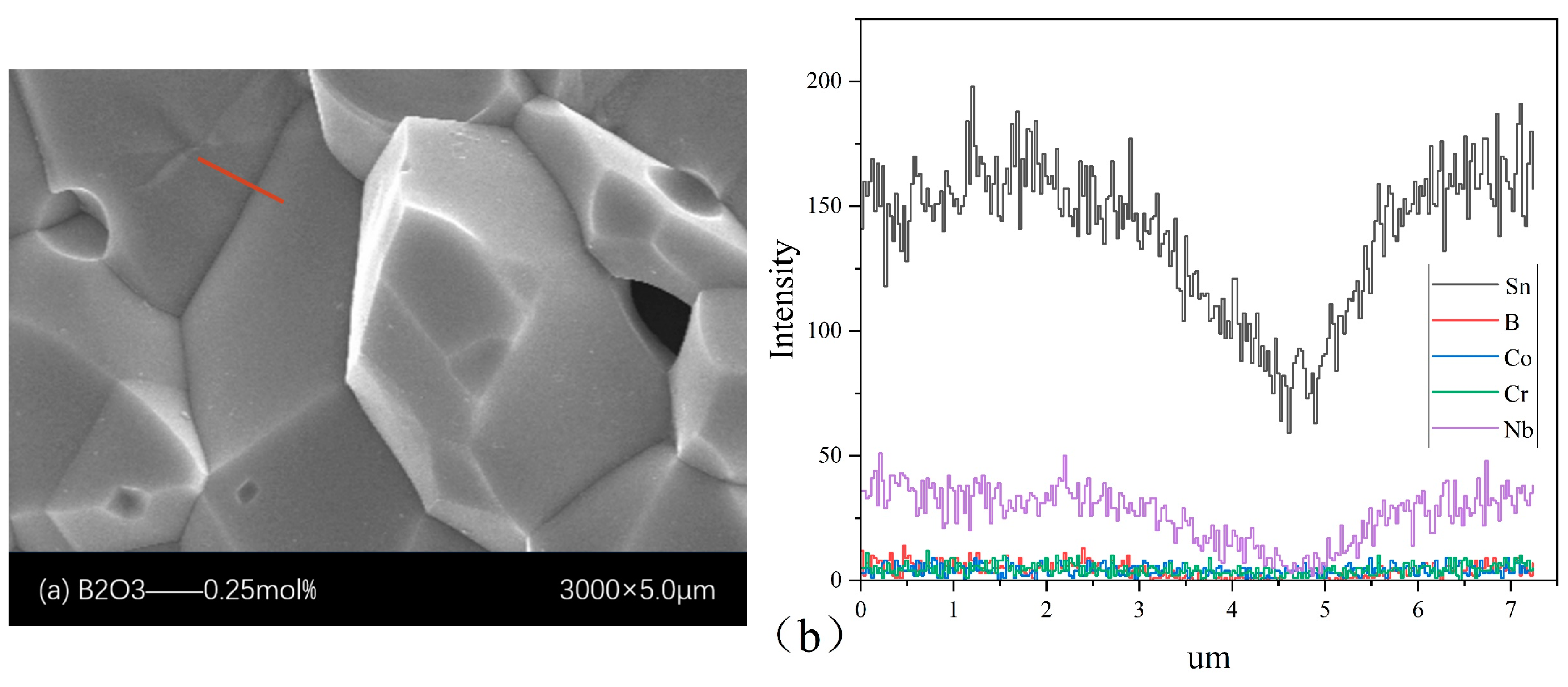
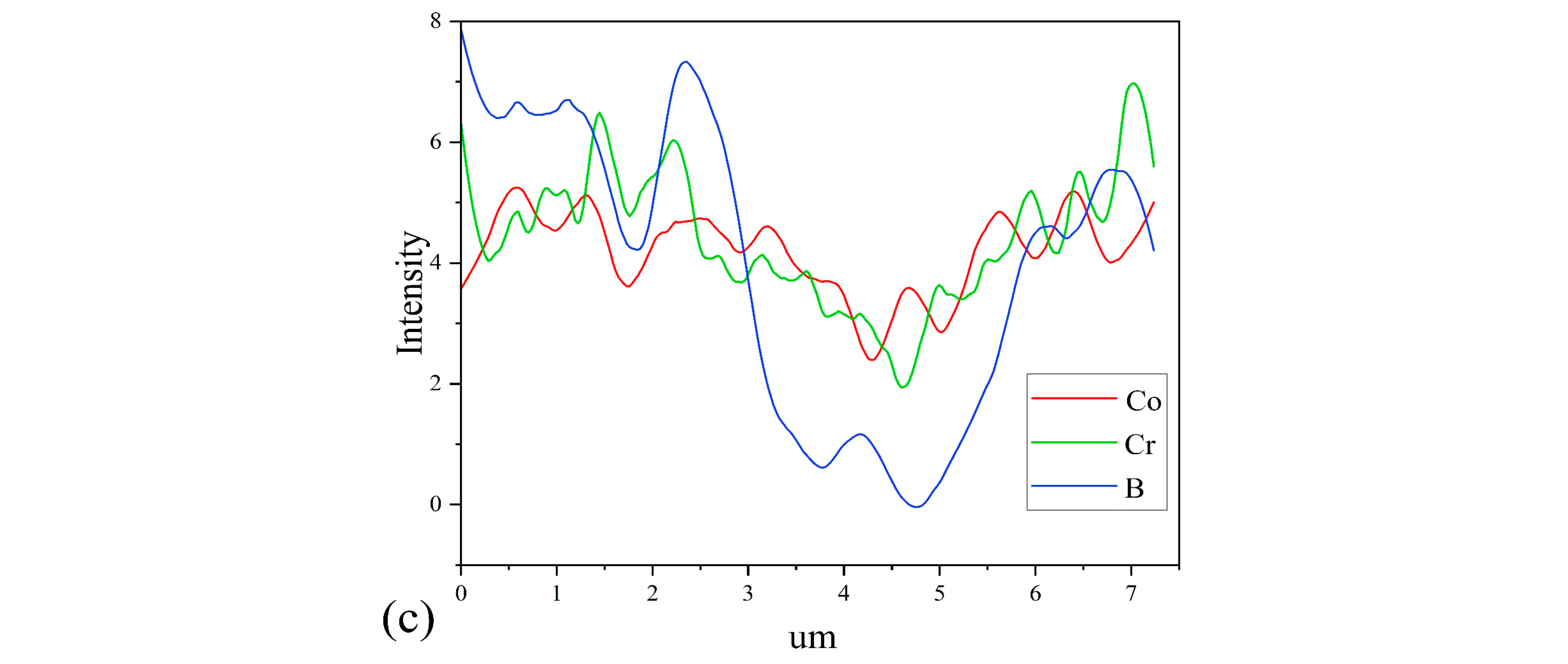
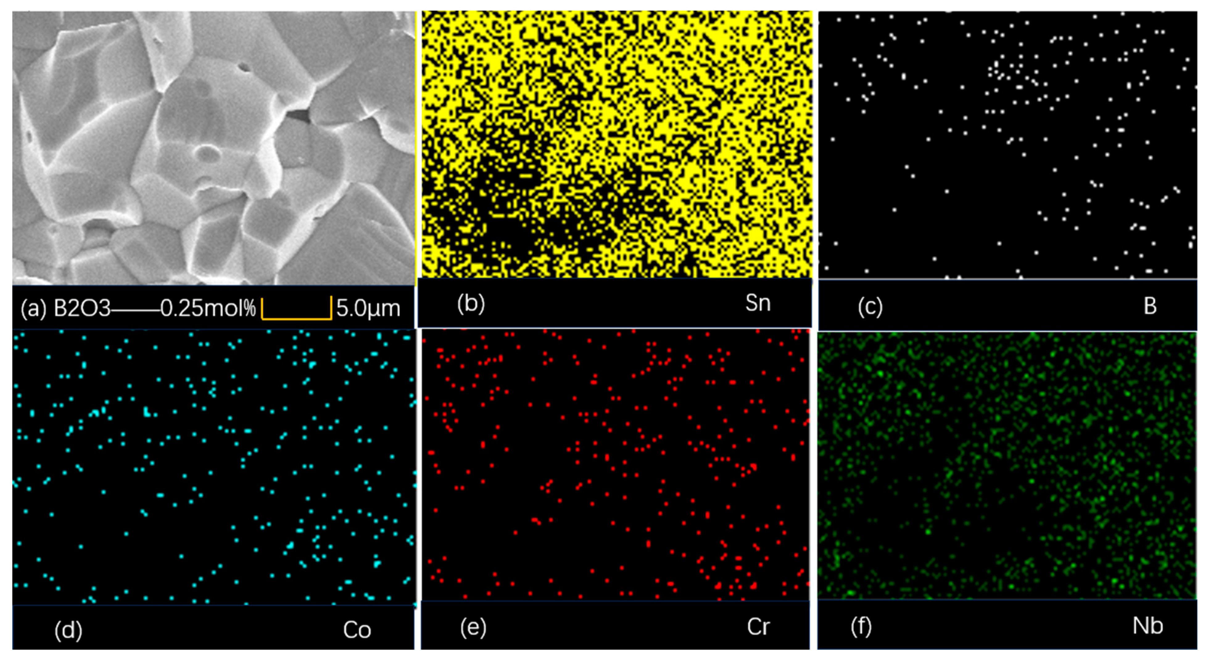
4.1. Microstructure

Scanning electron microscope images (SEM) of SnO2 varistor samples prepared with different doping concentrations are shown in Figure 2a–e. The average grain size d of the samples is shown in Table 1. The cross-sectional microstructures of SnO2 varistor samples without the addition of B2O3 and varistor samples doped with 0.05 mol% B2O3 are shown in Figure 2a,b, respectively. A large number of air gaps could be seen in the samples, and the grain sizes were uneven.
When the addition amounts of B2O3 were 0.15 mol% and 0.25 mol%, the grain sizes of the varistor samples increased significantly compared with those of the undoped samples, and the porosity of the samples decreased. This indicated that a small amount of B2O3 could improve the uniformity and density of the samples. At the same time, due to the melting of low-melting-point B2O3 into a liquid state during high-temperature sintering, the flowability of SnO2 grains was promoted, the liquid-phase sintering time was prolonged, and it was easier to grow. The extension of the liquid-phase sintering time resulted in a more uniform distribution of the modifiers Co3O4, Cr2O3, and Nb2O5 in the sample.
The ionic radius of B3+ (0.23 Å) was much smaller than that of Sn4+ (0.69 Å), so during the sintering process, B2O3 might have reacted with SnO2 grains in the solid solution, i.e., B3+ replaced the position of Sn4+ to produce host defects within the SnO2 grains, as described in Equation (8), and the resulting oxygen vacancies accelerated the mass transfer of SnO2, which facilitated the sintering of SnO2, thus making the resulting SnO2 samples denser [25].
B 2 O 3 S n O 2 2 B S n + V O · · + 3 O O X
With the added amount of B2O3 being 0.35 mol%, the porosity of the sample increased because the excess B2O3 could not enter the interior of the grains, so it segregated at the grain gaps, resulting in a decrease in density at the grain gaps.
Additionally, abnormal grains can be observed in Figure 2e, which reduced the uniformity of the sample. During the sintering process, the reaction shown in Equation (9) might have occurred, and a small amount of oxygen overflow was generated in the sample, leaving pores and increasing the porosity of this sample.
B 2 O 3 1300   ° C 2 B O + 1 2 O 2 g
Figure 3 shows the variation in elemental content in the EDS line scan. The straight line in Figure 3a represents the EDS line scan position, and Figure 3b shows the curve of the elemental content variation with position. When the line scanning distance is 4.68 μm, the content of all elements significantly decreases, indicating that 4.68 μm is the boundary between two grains. Due to the significantly higher content of Sn and Nb in the sample compared to other elements, the B, Co, and Cr content curves were smoothed for ease of observation, as shown in Figure 3c. It could be observed that Co and Cr were evenly distributed at both the grain and grain boundaries, with the Co and Cr contents being slightly lower at the grain boundaries than at the grains, indicating that Co and Cr mainly entered the lattice positions where they replaced Sn. The processes in Equations (10)–(14) had occurred.
C r 2 O 3 S n O 2 2 C r S n + V O · · + 3 O O X
2 N b 2 O 5 S n O 2 4 N b S n · + V S n + 10 O O X
C o 3 O 4 1300   ° C C o O + C o 2 O 3
C o 2 O 3 S n O 2 2 C o S n + V O · · + 3 O O X
C o O S n O 2 C o S n + V O · · + O O X
However, B was predominantly present in the grains, suggesting that B entered the grains during the sintering and took the place of Sn, which proved that the process in Equation (8) took place.
The elemental surface EDS analysis of the specimens with the B2O3 addition of 0.25 mol% is shown in Figure 4, and the results indicate that B3+ ions are doped into the SnO2 lattice. The addition of B2O3 promotes a uniform distribution of grains and a densified microstructure, which results in a grain size of 7.4 μm and a reduction in porosity to 4.2%, as shown in Table 1.

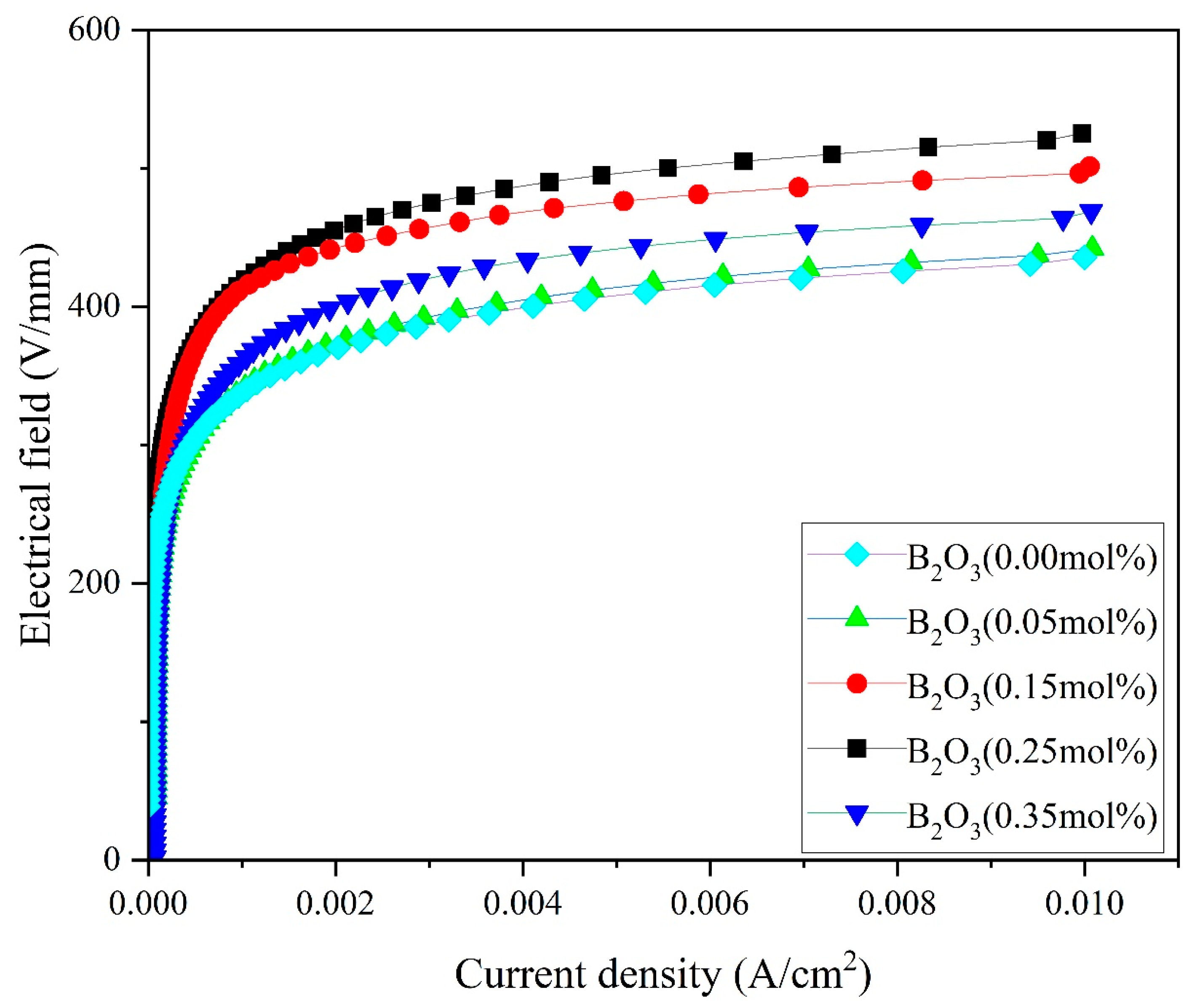
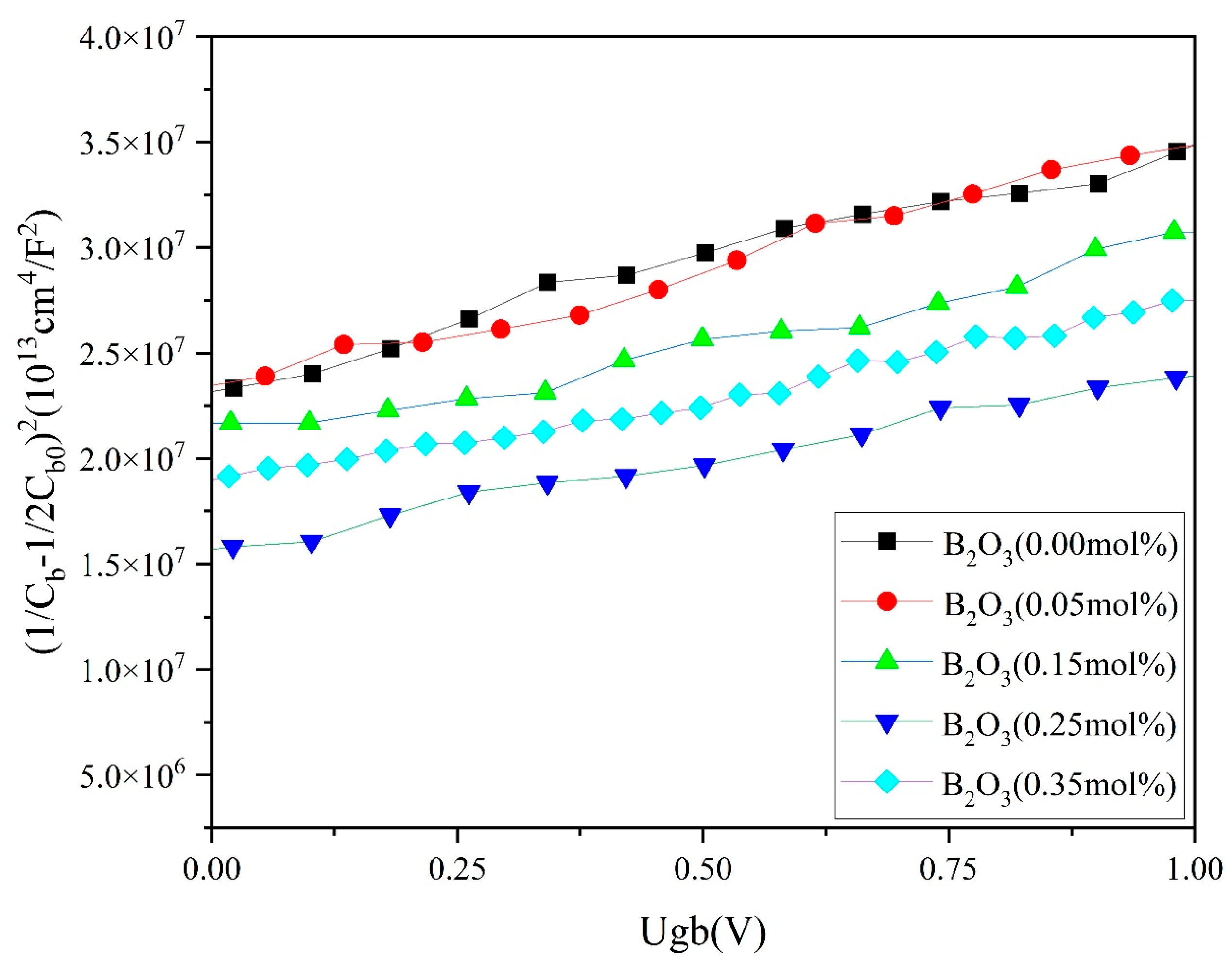
4.2. Electrical Characteristics

Figure 5 and Figure 6 show the I–V and C–V curves of the samples, and the voltage gradient E1 mA, nonlinearity coefficient α, leakage current JL, donor concentration N d , interfacial state density N i , and the potential barrier height φ b of the varistor were calculated from Equations (2)–(4) and listed in Table 1.
As could be derived from the data in Figure 5, with the increase in the B2O3 addition in the SnO2 varistor from 0.00 mol% to 0.35 mol%, as shown in Table 1, the voltage gradient of the varistor first increased and then decreased with the doping concentration. When the B2O3 doping concentration was 0.25 mol%, the voltage gradient of the varistor sample reached a maximum of 525 V/mm. At this concentration, the leakage current was minimized to 11.2 μA/cm2, and the nonlinear coefficient was maximized to 36.
The doping of B2O3 in SnO2 varistors reacted as shown in Equations (8) and (9), and the doping of Co3O4, B2O3, Cr2O3, and Nb2O5 introduced a large number of defects such as C o S n ,   C o S n , C r S n , V S n , V O · · , N b S n · in Equations (10)–(14) [26,27].
A large number of oxygen vacancies were generated during the reaction process, which easily ionized free electrons and enhanced the N-type semiconductor properties of the SnO2 material. Therefore, the introduction of impurities and defects to the SnO2 semiconductor doped with Co3O4, Nb2O3, and Cr2O3 increased the nonlinear coefficient of the sample.
Figure 6 shows the capacitance–voltage (C–V) characteristics of the samples with different B2O3 contents. The N d , φ b , and N i of samples could be obtained from the characteristic curves by Equations (3) and (4), and the results are summarized in Table 1. It can be seen from Table 1 that the N i , N d , and φ b all showed a trend of increasing and then decreasing with the gradual increase in the B2O3 doping concentration. Equation (8) shows that a portion of B3+ reacted with Sn4+ in a defective way to produce B S n , which contributed to the formation of Schottky barriers. B2O3 as an acceptor dopant increased the hole concentration in the sample, resulting in an increase in Nd. The change in N i was due to the doping of low-melting-point B2O3, which lowered the starting temperature of liquid-phase sintering, prolonged the sintering time of the liquid phase, promoted oxygen transfer, and increased the oxygen content in the sample.
According to Equation (4), it could be seen that when the increase in the interface state concentration was greater than the donor density, the width of the depletion layer could be widened, leading to an increase in the grain boundary potential barrier. When the doping concentration of B2O3 was 0.25%, the maximum value of φ b was 1.24 eV. This was because a small amount of B2O3 doping promoted ion exchange between the grains and other additives at the grain boundaries in the varistor, which helped to increase the barrier height and reduce leakage current. When the doping concentration of B2O3 was 0.35 mol%, both the voltage gradient and nonlinear coefficient decreased because the increase in grain size led to a decrease in the number of unit grain boundaries, resulting in a decrease in grain boundary potential barriers and voltage gradients.

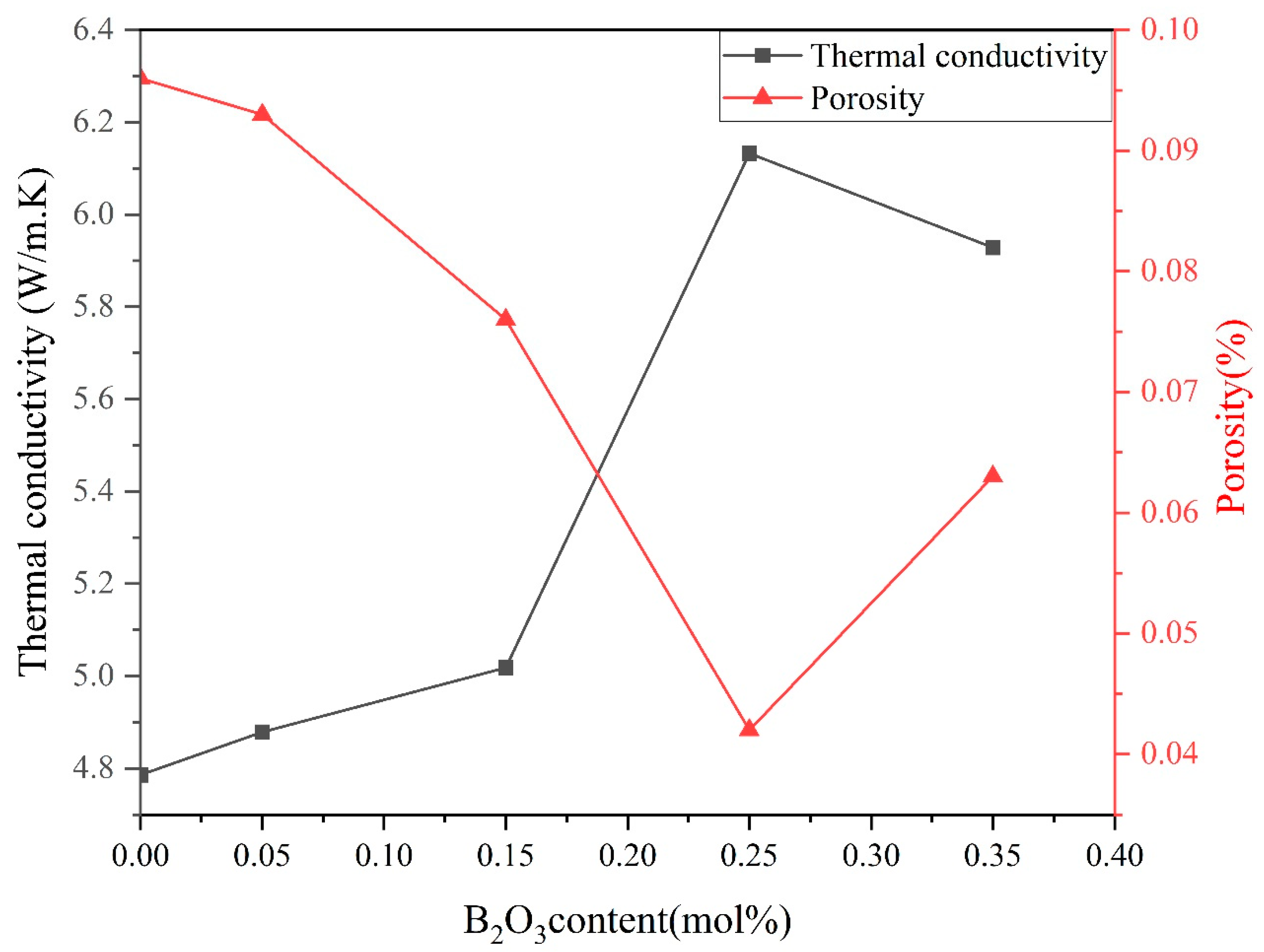
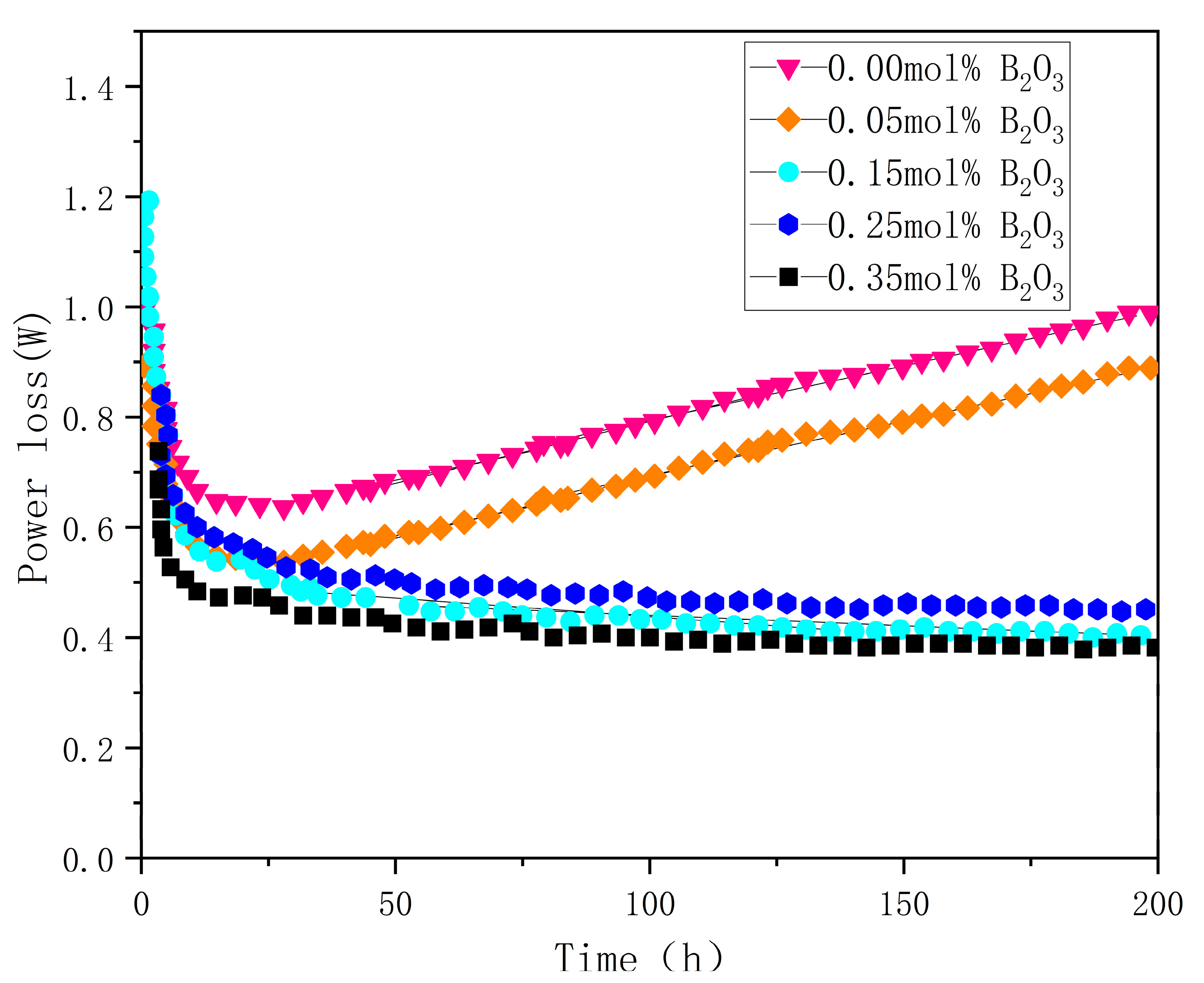
4.3. Thermal Conductivity

When the doping concentration of B2O3 increased from 0.00 mol% to 0.15 mol%, the thermal conductivity also increased from 4.88 W/m·K to 5.02 W/m·K. When the doping concentration of B2O3 was 0.25 mol%, the maximum thermal conductivity was 6.13 W/m·K, and as the doping concentration further increased, the thermal conductivity decreased to 5.93 W/m·K.
According to Equation (7), the presence of defects such as point defects, grain boundaries, and dislocations increased the number of phonons, increased the probability of phonon collisions, further enhanced phonon scattering, changed the initial heat transfer direction of phonons, and released their energy. At the same time, collisions caused energy loss and weakened or terminated phonon transmission, resulting in a decrease in the mean free path of phonons in the varistor samples and a decrease in thermal conductivity efficiency. Phonon scattering was inversely proportional to thermal conductivity efficiency.
When the grain size increased, the number of grain boundaries through which heat transfer paths passed decreased, phonon scattering at grain boundaries decreased, and thermal conductivity efficiency increased accordingly. Based on the microstructure data of the sample in Table 1 and the variation in thermal conductivity in Figure 6, it could be concluded that as the B2O3 doping concentration in the sample increased from 0.00 mol% to 0.25 mol%, the grain size of the sample increased from 6.8 μm to 7.4 μm. Therefore, in the process of heat transfer, the number of grain boundaries traversed by the heat transfer path decreased as the grain size increased. In Equation (7), l b decreased with increasing doping concentration, resulting in a decrease in phonon scattering and an increase in thermal conductivity.
Phonon scattering occurred through the pores, and excessive porosity increased the energy loss in the phonon-scattering process, thus reducing the overall thermal conductivity of the sample [28,29]. When the doping concentration of B2O3 was increased to 0.35 mol%, the appearance of anomalous grains could be observed from Figure 2d, and the homogeneity of the sample was reduced. At the same time, too much B2O3 occurred as in Equation (9), and the resulting oxygen overflowed to form air holes during the sintering process, which reduced the densification of the sample and ultimately led to an increase in the porosity of the sample. The existence of pores made the number of phonons increase during the heat conduction process, and the probability of phonon collision increased, which increased the phonon scattering, i.e., l p ω in Equation (7) increased, which ultimately led to a decrease in the thermal conductivity of the sample, thus adversely affecting the heat dissipation of the varistor.
From Figure 7, it can be obtained that the porosity of the varistor samples was inversely proportional to the thermal conductivity when B2O3 doping was increased from 0.00 mol% to 0.35 mol%. Additionally, it can be concluded that the main factor affecting the thermal conductivity under this experimental formulation was the porosity.
The varistor had the lowest porosity and the highest thermal conductivity when B2O3 doping was 0.25 mol%, which meant that the efficiency of heat transfer of the samples in this formulation was the greatest and had good heat dissipation performance.
As depicted in Figure 8, to assess the impact of B2O3 doping on SnO2 varistors, 200 h DC accelerated aging tests were performed on samples with doping levels of 0, 0.05, 0.15, 0.25, and 0.35 mol%. The results indicated that samples doped with 0 and 0.05 mol% exhibited a gradual increase in power loss over time. This was attributed to the high leakage current density, which induced heating in the varistor ceramics under DC bias. Given their negative temperature coefficient, leakage currents escalated, leading to thermal runaway. In contrast, samples doped with 0.15, 0.25, and 0.35 mol% showed an initial peak in power loss, followed by a gradual decrease to a stable value as time progressed. This stabilization resulted from an increased barrier height, primarily caused by the realignment of ions at grain boundaries under the applied voltage, which broadened the depletion layer. These findings demonstrated that appropriate B2O3 doping significantly improved the aging stability of SnO2 varistors.

5. Conclusions

This study systematically investigated the synergistic optimization mechanism of B2O3 doping on the electrical properties and thermal conductivity of SnO2-Co3O4-Cr2O3-Nb2O5-B2O3 varistors. The experimental results demonstrated that the sample with 0.25 mol% B2O3 exhibited optimal comprehensive performance: a voltage gradient of 525 V/mm, a nonlinear coefficient of 36, a leakage current density as low as 11.2 μA/cm2, and a thermal conductivity of 6.13 W·m−1·K−1. Microstructural analysis revealed that moderate B2O3 doping facilitated grain densification and liquid-phase sintering homogeneity through solid solution substitution of Sn4⁺ (generating oxygen vacancy defects), which significantly reduced porosity (4.2%) and increased grain size (7.4 μm). The simultaneous enhancement of grain boundary barrier height (φb = 1.24 eV) and interfacial state density (Ni = 6.8 × 10¹⁵ m−2) effectively suppressed leakage currents and strengthened nonlinear responses. Furthermore, grain coarsening reduced phonon-scattering paths, while low porosity decreased thermal resistance, synergistically improving thermal conductivity by 25.6% compared to undoped samples. This study provides a theoretical foundation for developing SnO2-based varistors with high electrical performance and thermal stability, which can be extended to the insulation design optimization of surge arresters in ultra-high-voltage power grids. Future work should explore long-term aging behavior under multi-field coupling (e.g., temperature–electric field–mechanical stress) and validate process reproducibility in industrial-scale production.

Author Contributions

S.G.: formal analysis; H.Z.: supervision, writing—review and editing. All authors have read and agreed to the published version of the manuscript.

Funding

This research was funded by Natural Science Foundation of Xinjiang Uygur Autonomous Region grant number No. 2022D01C21.

Institutional Review Board Statement

Not applicable.

Informed Consent Statement

Not applicable.

Data Availability Statement

The original contributions presented in this study are included in the article. Further inquiries can be directed to the corresponding author.

Conflicts of Interest

The authors declare that they have no known competing financial interests or personal relationships that could have appeared to influence the work reported in this paper.

References

  1. Li, Z.; Yu, Z.; He, J.; Peng, X.; Li, Z. Analysis of Lightning Protection Performance Improvement for Multi-Circuit Lines on the Same Tower Using Transmission Line Arresters. High Volt. Eng. 2011, 37, 3120–3128. [Google Scholar]
  2. Dong, C.; Jianhua, L.; Chenxi, J. Study on lightning resistance level based on ATP-EMTP. Electr. Porcelain Surge Arrester 2011, 53, 47–50. [Google Scholar]
  3. Shahraki, M.M.; Mahmoudi, P.; Abdollahi, M.; Ebadzadeh, T. Fne-grained SnO2 varistors prepared by microwave sintering for ultra- high voltage applications. Mater. Lett. 2018, 230, 9–11. [Google Scholar] [CrossRef]
  4. Meng, P.; Hu, J.; Wu, J.; He, J. Multi-element doping comprehensive regulation of comprehensive performance of zinc oxide varistor. High Volt. Technol. 2018, 44, 241–247. [Google Scholar]
  5. Ferreira, T.V.; Bolacell, G.S.; da Rosa, M.A.; da Costa, E.G.; Lira, G.R.; Pissolato, J.F.; Andrade, F.L.; Ferreira, R.S.; Neto, E.T.W.; Francisco, R.P. Technological Development of a Composite Insulator for High Voltage Transmission Line Monitoring. IEEE Electr. Insul. Mag. 2023, 39, 7–16. [Google Scholar]
  6. Jinhua, Z. Optimization study on voltage level and transmission capacity. IEEE Trans. Power Syst. 2009, 24, 193–197. [Google Scholar]
  7. Bueno, P.R.; Varela, J.A.; Barrado, C.M.; Longo, E.; Leite, E.R. A Comparative Study of Thermal Conductivity in ZnO- and SnO2-Based Varistor Systems. J. Am. Ceram. Soc. 2005, 88, 2629–2631. [Google Scholar]
  8. Wei, Q.; He, J.; Hu, J.; Wang, Y. Influence of Cr2O3 on the residual voltage ratio of SnO2-based varistor. J. Am. Ceram. Soc. 2011, 94, 1999–2002. [Google Scholar] [CrossRef]
  9. Mahmoudi, P.; Nemati, A.; Shahraki, M.M. Gra in growth kinetics and electrical properties of CuO doped SnO2 -based varistors. J. Alloys Compd. 2019, 770, 784–791. [Google Scholar]
  10. Cheng, K.; Zhao, H.; Zhou, Y. The Influence of Co doping of Y2O3, Ga2O3, and B2O3 on the Microstructure and Electrical Properties of ZnO Varistors. High Volt. Technol. 2023, 49, 4707–4716. [Google Scholar]
  11. Pianaro, S.A.; Bueno, P.R.; Olivi, P.; Longo, E.; Varela, J.A. Electrical properties of the SnO2-based varistor. J. Mater. Sci. Lett. 1997, 16, 634–638. [Google Scholar]
  12. Pianaro, S.A.; Bueno, P.R.; Longo, E.; Varela, J.A. A new SnO2-based varistor system. J. Mater. Sci. Lett. 1995, 14, 692–694. [Google Scholar] [CrossRef]
  13. Xin, L. Simulation of the Conductive Process of Nano ZnO Varistors Based on Animation Plane Form. J. Chem. 2020, 2020, 9726173. [Google Scholar]
  14. Hembram, K.; Rao, T.N.; Ramakrishana, M.; Srinivasa, R.S.; Kulkarni, A.R. Influence of Cao Doping on Phase, Microstructure, Electrical and Dielectric Properties of Zno Varistors. J. Technol. 2020, 817, 152700. [Google Scholar] [CrossRef]
  15. Hembram, K.; Rao, T.N.; Ramakrishna, M.; Srinivasa, R.S.; Kulkarni, A.R. A Novel Economical Grain Boundary Engineered Ultra-high Performance Zno Varistor with Lesser Dopants. J. Technol. Sci. 2019, 38, 5021–5029. [Google Scholar]
  16. Bueno, P.R.; Leite, E.R.; Oliveira, M.M.; Orlandi, M.O.; Longo, E. Role of oxygen at the grain boundary of metal oxide varistors: A potential barrier formation mechanism. Appl. Phys. Lett. 2001, 79, 48. [Google Scholar] [CrossRef]
  17. Tsuboi, T.; Takami, J.; Okabe, S.; Kido, T.; Maekawa, T. Energy absorption capacity of a 500 kV surge arrester for direct and multiple lightning strokes. IEEE Trans. Dielectr. Electr. Insul. 2015, 22, 916–924. [Google Scholar] [CrossRef]
  18. Tominc, S.; Rečnik, A.; Samardžija, Z.; Dražić, G.; Podlogar, M.; Bernik, S.; Daneu, N. Twinning and charge compensation in Nb2O5-doped SnO2-CoO ceramics exhibiting promising varistor characteristics. Ceram. Int. 2018, 44, 1603–1613. [Google Scholar]
  19. Wurst, J.C.; Nelson, J.A. Lineal Intercept Technique for Measuring Grain Size in Two-Phase Polycrystalline Ceramics. J. Am. Ceram. Soc. 1972, 55, 109. [Google Scholar]
  20. Mukae, K.; Tsuda, K.; Nagasawa, I. Capacitance-vs-voltage characteristics of ZnO varistors. J. Appl. Phys. 1979, 50, 4475–4476. [Google Scholar]
  21. Zhao, H.; He, J.; Hu, J.; Chen, S.; Xie, Q. High nonlinearity and low residual-voltage ZnO varistor ceramics by synchronously doping Ga2O3 and Al2O3. Mater. Lett. 2016, 164, 80–83. [Google Scholar] [CrossRef]
  22. Paul, G.; Chopkar, M.; Manna, I.; Das, P.K. Techniques for measuring the thermal conductivity of nanofluids: A review. Renew. Sustain. Energy Rev. 2010, 14, 1913–1924. [Google Scholar]
  23. Wu, J.W.; Sung, W.F.; Chu, H.S. Thermal conductivity of polyurethane foams. Int. J. Heat Mass Tran. 1999, 42, 2211–2217. [Google Scholar]
  24. Knacke, O.; Kubaschewski, O.; Hesselmann, K. (Eds.) Thermochemical Properties of Inorganic Substances, 2nd ed.; Springer: Berlin, Germany, 1976. [Google Scholar]
  25. Yang, X.; Zhao, H.; Wu, Y.; Zhao, Q. Effect of sintering temperature on microstructure and electrical properties of SnO2 varistor doped with B2O3. Electr. Porcelain Light. Arrester 2023, 5, 72–76. [Google Scholar] [CrossRef]
  26. Miranda-López, M.I.; Padilla-Zarate, E.A.; Hernández, M.B.; Falcón-Franco, L.A.; García-Villarreal, S.; García-Quiñonez, L.V.; Zambrano-Robledo, P.; Toxqui-Terán, A.; Aguilar-Martínez, J.A. Comparison between the use of Co3O4 or CoO on microstructure and electrical properties in a varistor system based on SnO2. J. Alloys Compd. 2020, 824, 153952. [Google Scholar]
  27. Goh, W.F.; Yoon, T.L.; Khan, S.A. Molecular dynamics simulation of thermodynamic and thermal transport properties of strontium titanate with improved potential parameters. Comput. Mater. Sci. 2012, 60, 123–129. [Google Scholar]
  28. Clarke, D.R. Materials selection guidelines for low thermal conductivity thermal barrier coatings. Surf. Coat. Technol. 2003, 163, 67–74. [Google Scholar]
  29. Chen, Y.; Jiang, P.; Zhang, R.; Sun, J.; Zhang, B.; Zhang, Y. Effect of porosity on thermal conductivity of five-component ceramic system. J. Aeronaut. Mater. 2023, 543, 66–74. [Google Scholar]
Figure 1. Tin oxide varistor production process flow chart.
Materials 18 01399 g001
Figure 2. Scanning electron microscope images of different B2O3 contents in SnO2.
Materials 18 01399 g002
Figure 3. (a) SEM microstructure (The red line is the EDS scanning position). (b) Schematic of the distribution of the elements in the orange straight line position of the EDS line sweep in the microstructure. (c) EDS scan elemental distribution of Co, Cr, and B elements.
Materials 18 01399 g003aMaterials 18 01399 g003b
Figure 4. EDS elemental distribution map.
Materials 18 01399 g004
Figure 5. IV curves of SnO2 samples doped with different amounts of B2O3.
Materials 18 01399 g005
Figure 6. Capacitance–voltage (C–V) characteristics of samples doped with different contents of B2O3.
Materials 18 01399 g006
Figure 7. Curves of SnO2 porosity and thermal conductivity efficiency with B2O3 doping at fixed temperature.
Materials 18 01399 g007
Figure 8. Changes in power loss of samples aged for 200 h.
Materials 18 01399 g008
Table 1. Microstructure and electrical properties of SnO2 with different B2O3 doping levels.
B2O3 (mol%)Porosity
%
d
(μm)
E1 mA
(V/mm)
JL
(μA/cm2)
αNd
(1022 m−2)
Ni
(1015 m−2)
Φb
(eV)
0.009.4%6.742125261.83.00.82
0.059.3%6.844823291.93.20.85
0.157.6%7.250118.3312.64.40.98
0.254.2%7.452511.2364.76.81.24
0.356.3%8.642814.6333.65.41.15
Disclaimer/Publisher’s Note: The statements, opinions and data contained in all publications are solely those of the individual author(s) and contributor(s) and not of MDPI and/or the editor(s). MDPI and/or the editor(s) disclaim responsibility for any injury to people or property resulting from any ideas, methods, instructions or products referred to in the content.

