Hydrazine-Assisted Formation of Indium Phosphide (InP)-Based Nanowires and Core-Shell Composites


Abstract
:
1. Introduction
2. Results and Discussion
2.1. Hydrazine-Assisted Gas Phase Formation of InP Nanowires
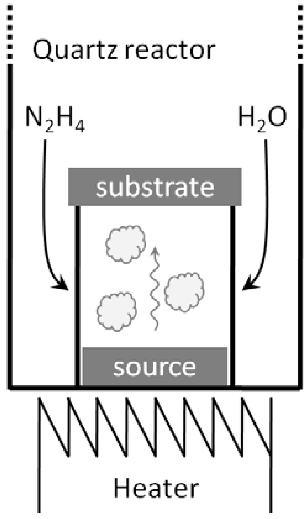
2.1.1. Experimental Parameters

2.1.2. Temperature-Morphology Relations among InP NWs


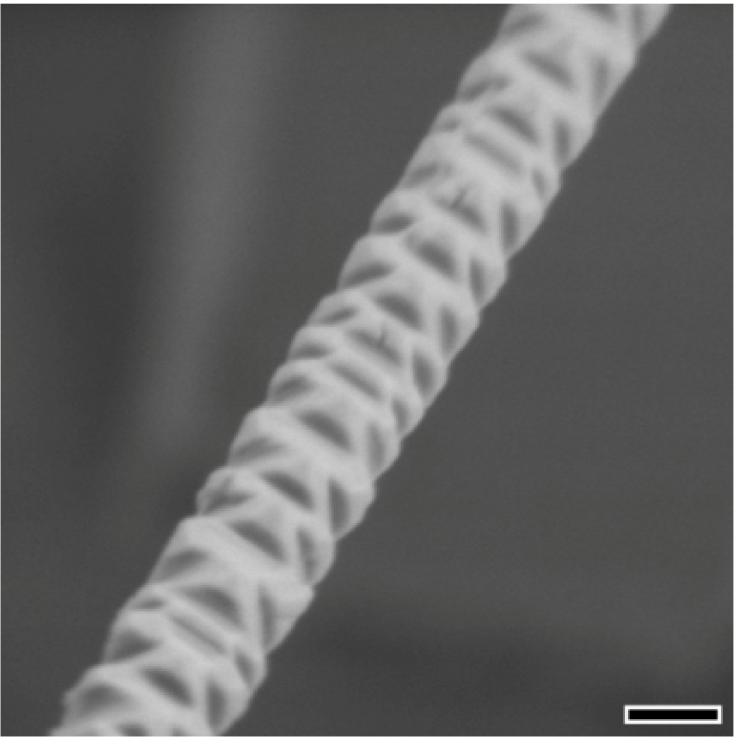
2.1.3. Zigzag Shaped InP Nanowires

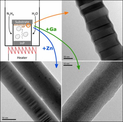
2.2. Mixed Nanowire Growth from InP–Ga Sources
2.2.1. Scope and Synthesis

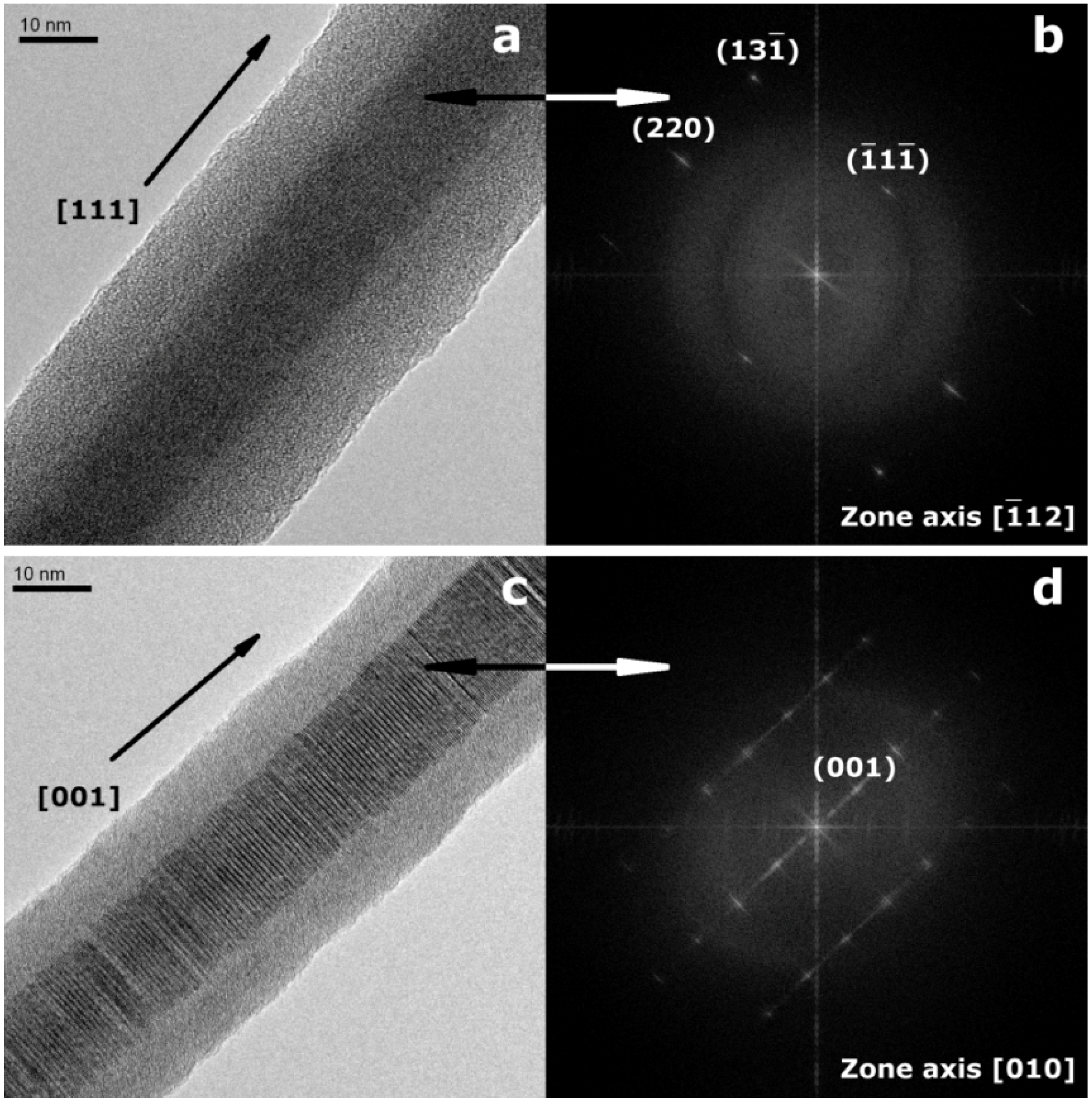
2.2.2. Structural Properties

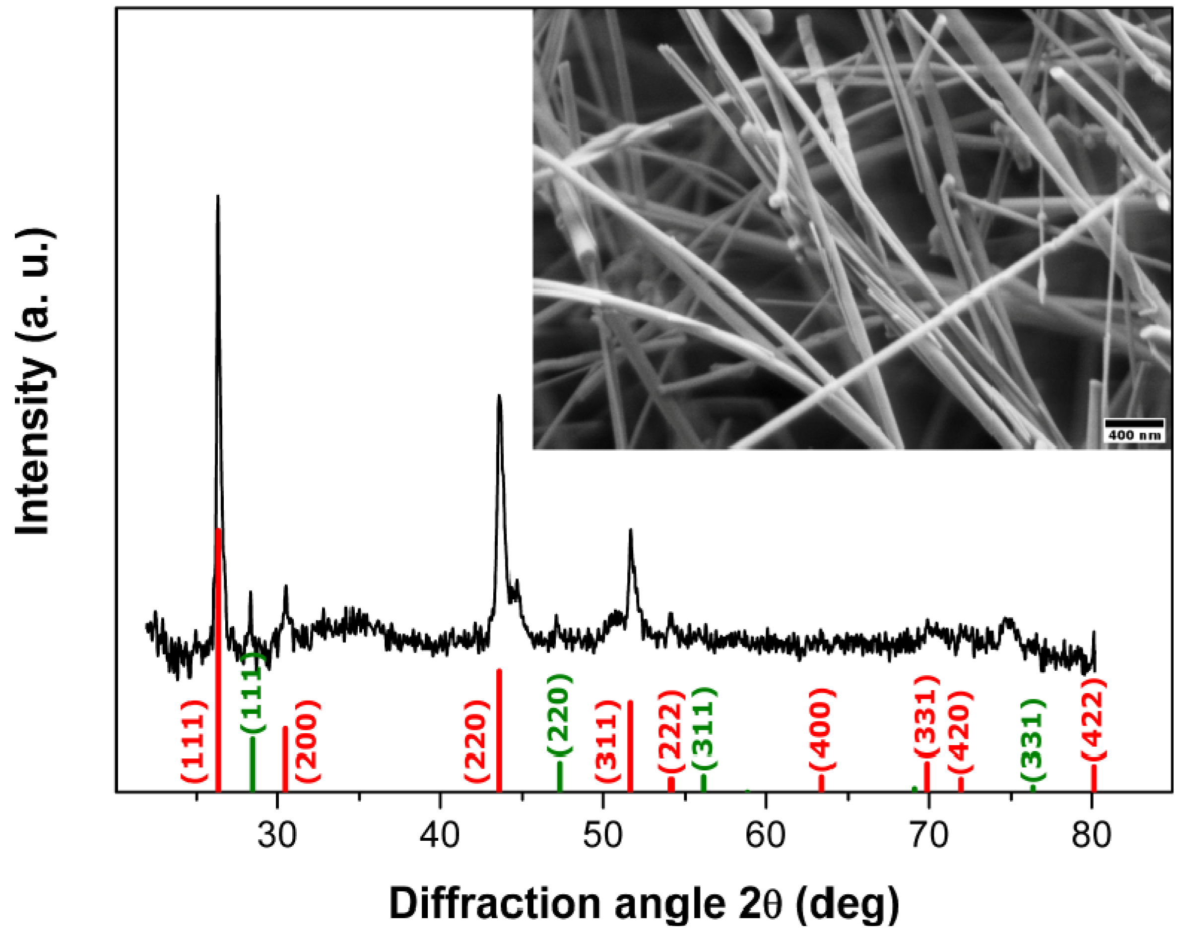
2.3. Hydrazine-Assisted Nanowire Growth from InP–Zn Source Materials
2.3.1. Scope and Synthesis
2.3.2. Influence of the Reaction Temperature


3. Experimental Section
3.1. Sample Preparation

3.2. Characterization
4. Conclusions
Supplementary Materials
Supplementary File 1Acknowledgments
References
- Dick, K.A. A review of nanowire growth promoted by alloys and non-alloying elements with emphasis on Au-assisted III–V Nanowires. Prog. Cryst. Growth Charact. Mater. 2008, 54, 138–173. [Google Scholar] [CrossRef]
- Mingo, N. Thermoelectric figure of merit and maximum power factor in III–V semiconductor nanowires. Appl. Phys. Lett. 2004, 84, 2652–2654. [Google Scholar] [CrossRef]
- Vurgaftman, I.; Meyer, J.R.; Ram-Mohan, L.R. Band parameters for III–V compound semiconductors and their alloys. J. Appl. Phys. 2001, 89, 5815–5875. [Google Scholar] [CrossRef]
- Riikonen, J.; Tuomi, T.; Lankinen, A.; Sormunen, J.; Säynätjoki, A.; Knuuttila, L.; Lipsanen, H.; McNally, P.J.; O'Reilly, L.; Danilewsky, A.; et al. Synchrotron X-ray topography study of defects in indium antimonide P–I–N structures grown by metal organic vapour phase epitaxy. J. Mater. Sci. Mater. Electron. 2005, 16, 449–453. [Google Scholar] [CrossRef]
- Chen, H.M.; Chen, C.K.; Lin, C.C.; Liu, R.-S.; Yang, H.; Chang, W.-S.; Chen, K.-H.; Chan, T.-S.; Lee, J.-F.; Tsai, D.P. Multi-bandgap-sensitized ZnO nanorod photoelectrode arrays for water splitting: An X-ray absorption spectroscopy approach for the electronic evolution under solar illumination. J. Phys. Chem. C 2011, 155, 21971–21980. [Google Scholar] [CrossRef]
- Agarwal, R. Heterointerfaces in semiconductor nanowires. Small 2008, 4, 1872–1893. [Google Scholar] [CrossRef] [PubMed]
- Gudiksen, M.S.; Lauhon, L.J.; Wang, J.; Smith, D.C.; Lieber, C.M. Growth of nanowire superlattice structures for nanoscale photonics and electronics. Nature 2002, 415, 617–620. [Google Scholar] [CrossRef] [PubMed]
- Diedenhofen, S.L.; Janssen, O.T.A.; Hocevar, M.; Pierret, A.; Bakkers, E.P.A.M.; Urbach, H.P.; Gómez Rivas, J. Controlling the directional emission of light by periodic arrays of heterostructured semiconductor nanowires. ACS Nano 2011, 5, 5830–5837. [Google Scholar] [CrossRef] [PubMed]
- Pettersson, H.; Zubritskaya, I.; Nghia, N.T.; Wallentin, J.; Borgström, M.T.; Storm, K.; Landin, L.; Wickert, P.; Capasso, F.; Samuelson, L. Electrical and optical properties of InP nanowire ensemble p+–i–n+ photodetectors. Nanotechnology 2012, 23, 135201–135205. [Google Scholar] [CrossRef] [PubMed]
- Kubota, E.; Ohmori, Y.; Sugii, K. Electrical and optical properties of Mg-, Ca-, and Zn-doped InP crystals grown by the synthesis, solute diffusion technique. J. Appl. Phys. 1984, 55, 3779–3784. [Google Scholar] [CrossRef]
- Shen, G.; Chen, P.-C.; Bando, Y.; Golberg, D.; Zhou, Ch. Pearl-like ZnS-decorated InP nanowire heterostructures and their electric behaviors. Chem. Mater. 2008, 20, 6779–6783. [Google Scholar] [CrossRef]
- Nakaema, M.K.K.; Godoy, M.P.F.; Brasil, M.J.S.P.; Iikawa, F.; Silva, D.; Sacilotti, M.; Decobert, J.; Patriarche, G. Optical and structural investigation of In1−xGaxP free-standing microrods. J. Appl. Phys. 2005, 98, 053506:1–053506:6. [Google Scholar] [CrossRef]
- Minot, E.D.; Kelkensberg, F.; van Kouwen, M.; van Dam, J.A.; Kouwenhoven, L.P.; Zwiller, V.; Borgström, M.T.; Wunnicke, O.; Verheijen, M.A.; Bakkers, E.P.A.M. Single quantum dot nanowire LEDs. Nano Lett. 2007, 7, 367–371. [Google Scholar] [CrossRef] [PubMed]
- Mohan, P.; Motohisa, J.; Fukui, T. Fabrication of InP/InAs/InP core-multishell heterostructure nanowires by selective area metalorganic vapor phase epitaxy. Appl. Phys. Lett. 2006, 88, 133105:1–133105:3. [Google Scholar]
- Bhunia, S.; Kawamura, T.; Fujikawa, S.; Nakashima, H.; Furukawa, K.; Torimitsu, K.; Watanabe, Y. Vapor-liquid-solid growth of vertically aligned InP nanowires by metalorganic vapor phase epitaxy. Thin Solid Films 2004, 464 465, 244–247. [Google Scholar] [CrossRef]
- Jishiashvili, D.; Kapaklis, V.; Devaux, X.; Politis, C.; Kutelia, E.; Makhatadze, N.; Gobronidze, V.; Shiolashvili, Z. Germanium nitride nanowires produced by thermal annealing in hydrazine vapor. Adv. Sci. Lett. 2009, 2, 40–44. [Google Scholar] [CrossRef]
- Ikejiri, K.; Kitauchi, Y.; Tomioka, K.; Motohisa, J.; Fukui, T. Zinc blende and wurtzite crystal Phase mixing and transition in indium phosphide nanowires. Nano Lett. 2011, 11, 4314–4318. [Google Scholar] [CrossRef] [PubMed]
- Wallentin, J.; Ek, M.; Wallenberg, L.R.; Samuelson, L.; Borgström, M.T. Electron trapping in InP nanowire FETs with stacking faults. Nano Lett. 2012, 12, 151–155. [Google Scholar] [CrossRef] [PubMed]
- Muruyama, M.; Nakayama, T. Chemical trend of band offsets at wurtzite/zincblende heterocrystalline semiconductor interfaces. Phys. Rev. B 1994, 49, 4710–4724. [Google Scholar] [CrossRef]
- Pemasiri, K.; Montazeri, M.; Gass, R.; Smith, L.M.; Jackson, H.E.; Yarrison-Rice, J.; Paiman, S.; Gao, Q.; Tan, H.H.; Jagadish, C.; Zhang, X.; Zou, J. Carrier dynamics and quantum confinement in type II ZB-WZ InP nanowire homostructures. Nano Lett. 2009, 9, 648–654. [Google Scholar] [CrossRef] [PubMed]
- Kriegner, D.; Wintersberger, E.; Kawaguchi, K.; Wallentin, J.; Borgström, M.T.; Stangl, J. Unit cell parameters of wurtzite InP nanowires determined by X-Ray diffraction. Nanotechnology 2011, 22, 425704:1–425704:7. [Google Scholar] [CrossRef]
- Wang, J.; Plissard, S.; Hocevar, M.; Vu, T.T.T.; Zehender, T.; Immink, G.G.W.; Verheijen, M.A.; Haverkort, J.; Bakkers, E.P.A.M. Position-controlled [100] InP nanowire arrays. Appl. Phys. Lett. 2012, 100, 053107:1–053107:3. [Google Scholar]
- Bao, J.; Bell, D.C.; Capasso, F.; Wagner, J.B.; Mårtensson, T.; Trägårdh, J.; Samuelson, L. Optical properties of rotationally twinned InP nanowire heterostructures. Nano Lett. 2008, 8, 836–841. [Google Scholar] [CrossRef] [PubMed]
- Ek, M.; Borgström, M.T.; Karlsson, L.S.; Hetherington, C.J.D.; Wallenberg, L.R. Electron image series reconstruction of twin interfaces in InP superlattice nanowires. Microsc. Microanal. 2011, 17, 752–758. [Google Scholar] [CrossRef] [PubMed]
- Pozuelo, M.; Zhou, H.; Lin, S.; Lipman, S.A.; Goorsky, M.S.; Hicks, R.F.; Kodambaka, S. Self-catalyzed growth of InP/InSb axial nanowire heterostructures. J. Cryst. Growth 2011, 329, 6–11. [Google Scholar] [CrossRef]
- Ngo, C.; Zhou, H.; Mecklenburg, M.; Pozuelo, M.; Regan, B.C.; Xiao, Q.F.; Shenoy, V.B.; Hicks, R.F.; Kodambaka, S. Effect of precursor flux on compositional evolution in InP1−xSbx nanowires grown via self-catalyzed vapor-liquid-solid process. J. Cryst. Growth 2011, 336, 14–19. [Google Scholar] [CrossRef]
- Shen, G.; Bando, Y.; Golberg, D. InP–GaP Bi-coaxial nanowires and amorphous GaP nanotubes. J. Phys. Chem. C 2007, 111, 3665–3668. [Google Scholar] [CrossRef]
- Sacilotti, M.; Decobert, J.; Sik, H.; Post, G.; Dumas, C.; Viste, P.; Patriarche, G. Structural studies of nano/micrometric semiconducting GaInP wires grown by MOCVD. J. Cryst. Growth 2004, 272, 198–203. [Google Scholar] [CrossRef]
- van Weert, M.H.M.; Helman, A.; van den Einden, W.; Algra, R.E.; Verheijen, M.A.; Borgström, M.T.; Immink, G.; Kelly, J.J.; Kouwenhoven, L.P.; Bakkers, E.P.A.M. Zinc incorporation via the vapor-liquid-solid mechanism into InP nanowires. J. Am. Chem. Soc. 2009, 131, 4578–4579. [Google Scholar] [CrossRef] [PubMed]
- Schmidt, T.M.; Venezuela, P.; Arantes, J.T.; Fazzio, A. Electronic and magnetic properties of Mn-doped InP nanowires from first principles. Phys. Rev. B 2006, 73, 235330:1–235330:5. [Google Scholar]
- Lee, Y.-K.; Medina, H.; Chiu, P.-W. Modifying optical properties of GaN nanowires by Ga2O3 overgrowth. J. Vac. Sci. Technol. B 2012, 30, 011802:1–011802:4. [Google Scholar]
- Xiao, H.; Pei, H.; Liu, J.; Cui, J.; Jiang, B.; Hou, Q.; Hu, W. Fabrication, characterization, and photocatalysis of GaN-Ga2O3 core-shell nanoparticles. Mater. Lett. 2012, 71, 145–147. [Google Scholar] [CrossRef]
- Jin, C.; Park, S.; Kim, H.; Lee, C. Ultrasensitive multiple networked Ga2O3-Core/ZnO-shell nanorod gas sensors. Sens. Actuators B 2012, 161, 223–228. [Google Scholar] [CrossRef]
- Nagarajan, L.; De Souza, R.A.; Samuelis, D.; Valov, I.; Börger, A.; Janek, J.; Becker, K.-D.; Schmidt, P.C.; Martin, M. A chemically driven insulator-metal transition in non-stoichiometric and amorphous gallium oxide. Nat. Mater. 2008, 7, 391–398. [Google Scholar] [CrossRef] [PubMed]
- Yamaguchi, S. Main group oxides—Making the transition. Nat. Mater. 2008, 7, 353–354. [Google Scholar] [CrossRef] [PubMed]
- Choi, J.-H.; Ham, M.-H.; Lee, W.; Myoung, J.-M. Fabrication and characterization of GaN/amorphous Ga2O3 nanocables through thermal oxidation. Solid State Commun. 2007, 142, 437–440. [Google Scholar] [CrossRef]
- Hirano, R.; Kanazawa, T.; Inoue, T. Electrical characteristics of Zn in heavily doped InP grown by the liquid-encapsulated czochralski technique. J. Appl. Phys. 1992, 71, 659–663. [Google Scholar] [CrossRef]
- Alemany, M.M.G.; Tortajada, L.; Huang, X.; Tiago, M.L.; Gallego, L.J.; Chelikowsky, J.R. Role of dimensionality and quantum confinement in p-type semiconductor indium phosphide quantum dots. Sens. Actuators B 2008, 78, 233101:1–233101:4. [Google Scholar]
- Alemany, M.M.G.; Huang, X.; Tiago, M.L.; Gallego, L.J.; Chelikowsky, J.R. The role of quantum confinement in p-type doped indium phosphide nanowires. Nano Lett. 2007, 7, 1878–1882. [Google Scholar] [CrossRef]
- van Weert, M.H.M.; Wunnicke, O.; Roest, A.L.; Eijkemans, T.J.; Yu Silov, A.; Haverkort, J.E.M.; 't Hooft, G.W.; Bakkers, E.P.A.M. Large redshift in photoluminescence of p-doped InP nanowires induced by Fermi-level pinning. Appl. Phys. Lett. 2006, 88, 043109:1–043109:4. [Google Scholar] [CrossRef]
- Algra, R.E.; Verheijen, M.A.; Borgström, M.T.; Feiner, L.-F.; Immink, G.; van Enckevort, W.J.P.; Vlieg, E.; Bakkers, E.P.A.M. Twinning superlattices in indium phosphide nanowires. Nature 2008, 456, 369–372. [Google Scholar] [CrossRef] [PubMed]
- Duan, Z.; Shi, W.; Chrostowski, L.; Huang, X.; Zhou, N.; Chai, G. Design and epitaxy of 1.5 µm InGaAsP-InP MQW material for a transistor laser. Opt. Express 2010, 18, 1501–1509. [Google Scholar] [CrossRef] [PubMed]
- Ogura, M.; Choi, S.W.; Furue, S.; Hayama, N.; Nishida, K. Effects of Zn doped mesa sidewall on GaIn enhanced InGaAs/InP heterobipolar phototransistor. IEEE J. Quantum Electron. 2010, 46, 214–219. [Google Scholar] [CrossRef]
- Purica, M.; Budianu, E.; Rusu, E.; Danila, M.; Gavrila, R. Optical and structural investigation of ZnO thin films prepared by chemical vapor deposition (CVD). Thin Solid Films 2002, 403, 485–488. [Google Scholar] [CrossRef]
- Ilegems, M.; Panish, M.B.; Arthur, J.R. Phase-equilibria and vapor-pressures in Ga + P system. J. Chem. Thermodyn. 1974, 6, 157–177. [Google Scholar] [CrossRef]
- Ren, F. III-Nitride based Semiconductor Electronics and Optical Devices and Thirty-Fourth State-of-the-Art Program on Compound Semiconductors (SOTAPOCS XXXIV): Proceedings of the International Symposia; The Electrochemical Society: Pennington, NJ, USA, 2001. [Google Scholar]
- Woo, R.L.; Xiao, R.; Kobayashi, Y.; Gao, L.; Goel, N.; Hudait, M.K.; Mallouk, T.E.; Hicks, R.F. Effect of twinning on the photoluminescence and photoelectrochemical properties of indium phosphide nanowires grown on silicon (111). Nano Lett. 2008, 8, 4664–4669. [Google Scholar] [CrossRef] [PubMed]
- Xiong, Q.; Wang, J.; Eklund, P.C. Coherent twinning phenomena: Towards twinning superlattices in III–V semiconducting nanowires. Nano Lett. 2006, 6, 2736–2742. [Google Scholar] [CrossRef] [PubMed]
- Shen, G.; Bando, Y.; Liu, B.; Tang, C.; Golberg, D. Unconventional zigzag indium phosphide single-crystalline and twinned nanowires. J. Phys. Chem. B 2006, 110, 20129–20132. [Google Scholar] [CrossRef] [PubMed]
- Tsuzuki, H.; Cesar, D.F.; de Sousa Dias, M.R.; Castelano, L.K.; Lopez-Richard, V.; Rino, J.P.; Marques, G.E. Tailoring electronic transparency of twin-plane 1D superlattices. ACS Nano 2011, 5, 5519–5525. [Google Scholar] [CrossRef] [PubMed]
- Byun, H.J.; Lee, J.C.; Yang, H. Solvothermal synthesis of InP quantum dots and their enhanced luminescent efficiency by post-synthetic treatments. J. Colloid Interface Sci. 2011, 355, 35–41. [Google Scholar] [CrossRef]
- Wang, S.Q.; Ye, H.Q. A plane-wave pseudopotential study on III–V zinc-blende and wurtzite semiconductors under pressure. J. Phys. Condens. Matter 2002, 14, 9579–9587. [Google Scholar] [CrossRef]
© 2013 by the authors; licensee MDPI, Basel, Switzerland. This article is an open access article distributed under the terms and conditions of the Creative Commons Attribution license (http://creativecommons.org/licenses/by/3.0/).
Share and Cite
Patzke, G.R.; Kontic, R.; Shiolashvili, Z.; Makhatadze, N.; Jishiashvili, D. Hydrazine-Assisted Formation of Indium Phosphide (InP)-Based Nanowires and Core-Shell Composites. Materials 2013, 6, 85-100. https://doi.org/10.3390/ma6010085
Patzke GR, Kontic R, Shiolashvili Z, Makhatadze N, Jishiashvili D. Hydrazine-Assisted Formation of Indium Phosphide (InP)-Based Nanowires and Core-Shell Composites. Materials. 2013; 6(1):85-100. https://doi.org/10.3390/ma6010085
Chicago/Turabian StylePatzke, Greta R., Roman Kontic, Zeinab Shiolashvili, Nino Makhatadze, and David Jishiashvili. 2013. "Hydrazine-Assisted Formation of Indium Phosphide (InP)-Based Nanowires and Core-Shell Composites" Materials 6, no. 1: 85-100. https://doi.org/10.3390/ma6010085
APA StylePatzke, G. R., Kontic, R., Shiolashvili, Z., Makhatadze, N., & Jishiashvili, D. (2013). Hydrazine-Assisted Formation of Indium Phosphide (InP)-Based Nanowires and Core-Shell Composites. Materials, 6(1), 85-100. https://doi.org/10.3390/ma6010085