Article

Low-Temperature Solution-Processed Gate Dielectrics for High-Performance Organic Thin Film Transistors

1
Department of Applied Materials Engineering, Hanbat National University, Daejeon 305-719, Korea
2
School of Electrical and Electronics Engineering, Chung-Ang University, Seoul 156-756, Korea
3
Department of Materials Chemistry and Engineering, Konkuk University, Seoul 143-701, Korea
*
Authors to whom correspondence should be addressed.
Materials 2015, 8(10), 6926-6934; https://doi.org/10.3390/ma8105352
Submission received: 27 August 2015 / Revised: 23 September 2015 / Accepted: 8 October 2015 / Published: 12 October 2015

Abstract

:
A low-temperature solution-processed high-k gate dielectric layer for use in a high-performance solution-processed semiconducting polymer organic thin-film transistor (OTFT) was demonstrated. Photochemical activation of sol-gel-derived AlOx films under 150 °C permitted the formation of a dense film with low leakage and relatively high dielectric-permittivity characteristics, which are almost comparable to the results yielded by the conventionally used vacuum deposition and high temperature annealing method. Octadecylphosphonic acid (ODPA) self-assembled monolayer (SAM) treatment of the AlOx was employed in order to realize high-performance (>0.4 cm2/Vs saturation mobility) and low-operation-voltage (<5 V) diketopyrrolopyrrole (DPP)-based OTFTs on an ultra-thin polyimide film (3-μm thick). Thus, low-temperature photochemically-annealed solution-processed AlOx film with SAM layer is an attractive candidate as a dielectric-layer for use in high-performance organic TFTs operated at low voltages.

1. Introduction

Solution-processed organic thin-film transistors (OTFTs) have attracted considerable scientific and industrial interest because of their potential application in low-cost flexible electronics, such as active-matrix displays [1], circuitry [2,3], chemical/biological sensors [4,5] and radio-frequency identification (RFID) cards [6]. While small-molecule-based organic electronic materials have exhibited noteworthy performance enhancement [7,8,9,10], semiconducting polymers have also undergone continuous refinement in terms of device performance in recent decades, particularly as regards carrier mobility and operational stability [11,12,13,14,15]. The significant improvement in the carrier mobility of these electronic devices can primarily be attributed to enhancement of the closely packed lamellae structures along the current paths. Further, this improved carrier mobility constitutes a promising opportunity for the application of organic polymers to entry-level organic electronics. For example, it can be expected that solution-processed semiconducting polymers could possibly replace the conventionally used inorganic vacuum-deposited amorphous silicon (a-Si) in switching devices for flexible electrophoretic displays, which require less stringent performance than other devices. However, it is not clear whether solution-processed semiconducting polymers will eventually become applicable to organic light-emitting diodes (OLEDs), which demand significantly higher carrier mobility than the aforementioned switching devices. Recent advancements in the molecular design and processing conditions of high-performance polymer semiconductors have indicated that these materials could fulfill the requirements of various high-end display and electronic-system applications. In order to take full advantage of these polymers from an industrial perspective, the development of low-cost, high-capacitance, and reliable gate dielectric layers is equally important to the development of the high-performance polymer semiconductors themselves [16,17,18,19,20]. The high capacitance and low leakage currents of dielectric layers permit low-voltage operation of semiconducting polymer devices, leading to low power consumption by organic devices containing these polymers. Compared to organic-based dielectric layers, solution-processed inorganic high-k dielectrics satisfy the high-capacitance requirement for solution-processed organic polymers more fully, because of their excellent polarizability and chemical stability [17,21,22,23]. Recently, low-temperature solution-processed AlOx sol-gel films exhibited the relative low leakage current of about 10−6 A/cm2 at 1 MV/cm [24,25,26], which is suitable for the operation as a gate dielectric layer. Our recent demonstration of the photochemical activation of a solution-processed AlOx layer for oxide semiconductor devices clearly indicated that dense metal–oxide–metal network formation and condensation at low temperature are readily realizable via a non-thermal activation method [27,28], which is critical in the case of a flexible substrate. Thus, this photochemical activation enables us to fabricate high-performance DPP-based organic polymer devices on a flexible substrate.
In this article, we employ a hybrid gate dielectric layer composed of a photochemically activated AlOx film covered by an octadecylphosphonic acid (ODPA) self-assembled monolayer (SAM) in a high-performance poly-[2,5-bis(2-decyltetradecyl)pyrrolo[3,4-c]pyrrole-1,9-(2H,5H)-dione-(E)-(1,2-bis(5-(thiophen-2-yl)selenophen-2-yl)ethene] (P-29-DPPDTSE) OTFT operated at low voltage (<5 V). ODPA SAM treatment of the AlOx dielectric surface is used to modify its surface properties, with close intermolecular interactions between neighboring backbones in the P-29-DPPDTSE polymer being favored. This hybrid stack of organic/inorganic materials exhibits low leakage current density with no abrupt breakdown for an applied bias voltage of up to 10 V. Therefore, we achieved high-performance OTFT on a 3-μm-thick flexible polyimide (PI) film.

2. Experimental Procedure

In order to prepare the sol-gel precursor for the high-k AlOx gate dielectric film, aluminum nitrate nonahydrate (Al(NO3)3·9(H2O)) (Sigma-Aldrich) was dissolved in 2-methoxyethanol at concentrations of 0.3 and 0.8 M, so as to yield solution-processed dielectric films with different thicknesses. Immediately after the precursors were dissolved in the solvent, the resultant solutions were vigorously stirred and kept at 70 °C for more than 12 h to enhance the hydrolysis. For AlOx film deposition, the solutions were spin-coated at 2000 rpm for 40 s onto sputtered Cr glass or a thin PI/glass substrate with a Cr gate electrode structure to yield metal–insulator–metal (M-I-M) or OTFT device structures, respectively. Hence, thin dielectric layers were formed. Then, the as-deposited samples were photochemically annealed using deep ultraviolet (DUV) annealing for 2 h under a continuous nitrogen flow at room temperature, so as to facilitate condensation and densification of the precursors and formation of the metal–oxide–metal bonding network. During the annealing process, it was observed that the sample temperature gradually increased up to 150 °C as a consequence of the direct thermal radiation, which was generated by a low-pressure mercury UV lamp. Au electrodes for the bottom-contacted devices were then patterned, and the surfaces of the AlOx dielectric layers were modified by immersing the substrates in the ODPA solution for more than 12 h. This caused the high-performance polymers to favor intermolecular interactions during the solution processing. Finally, P-29-DPPTDTSE polymer films (0.2-wt % chloroform) were prepared through the spin-casting of this polymer onto the substrates at 2000 rpm for 40 s. The resultant films were then annealed at 200 °C for 10 min in the nitrogen-filled glove box. The film thicknesses and surface morphologies of photochemically-annealed AlOx gate dielectric layers were examined by using the profilometer (KLA-Tencor) and non-contact mode atomic force microscopy (AFM) system (PSIA), respectively. For the electrical characterization of the aforementioned M-I-M and OTFT device structures, capacitance vs. frequency and leakage current density vs. applied bias behaviors were analyzed using an Agilent LCR meter 4284A and Agilent 4156C analyzer, respectively. The characteristics of the high-performance OTFTs were also examined using an Agilent 4156C semiconductor parameter analyzer. All the electrical measurements were conducted in air and in a dark environment.

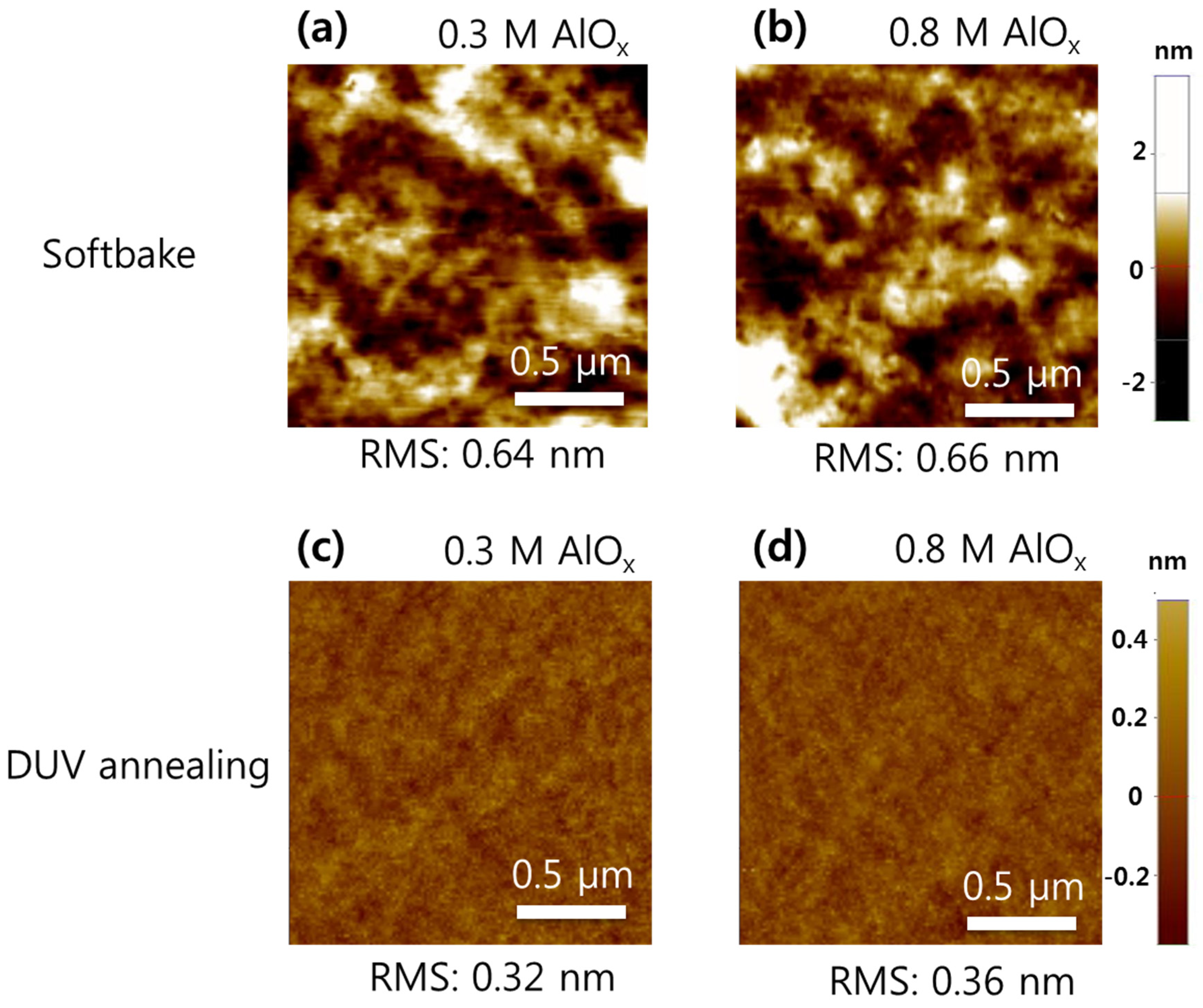
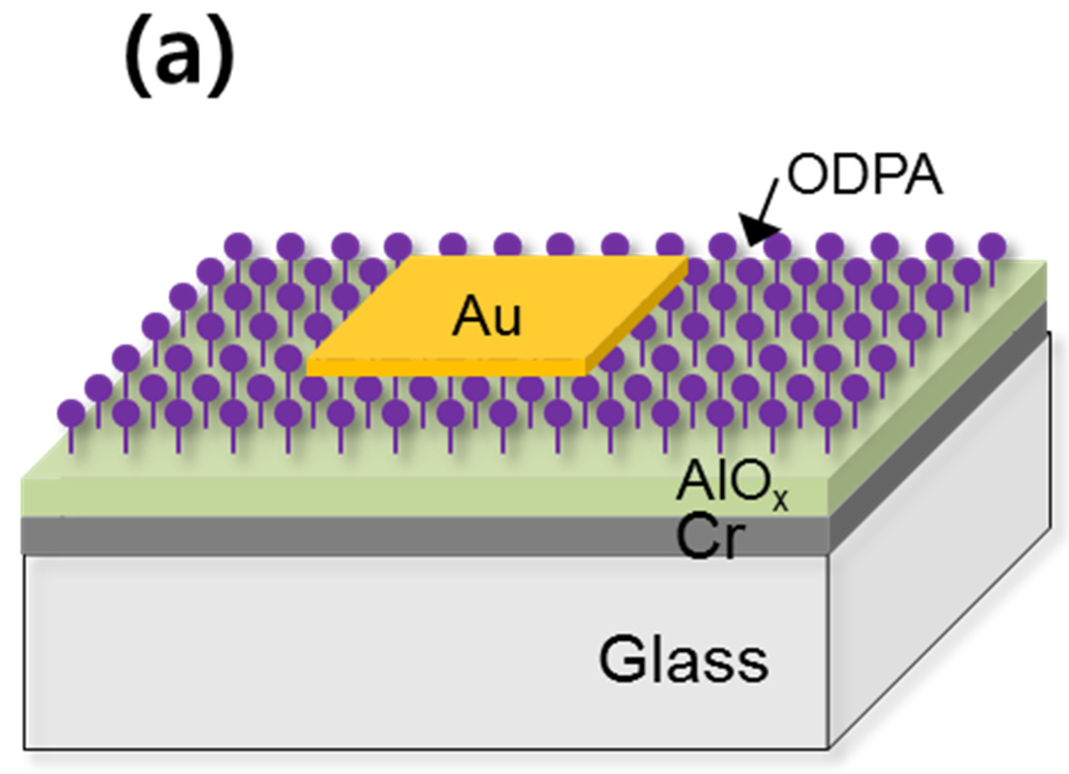
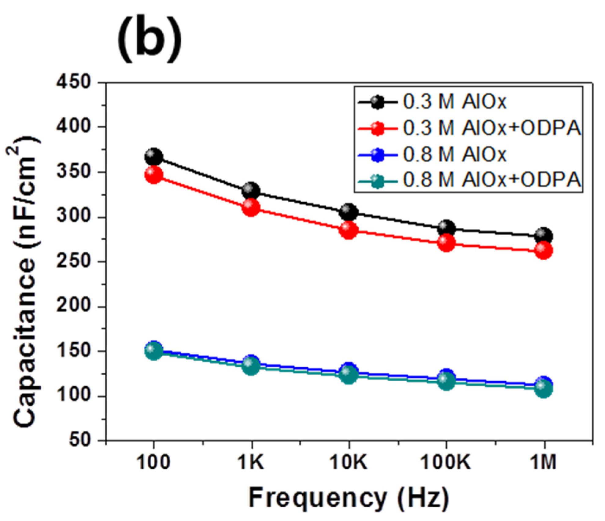
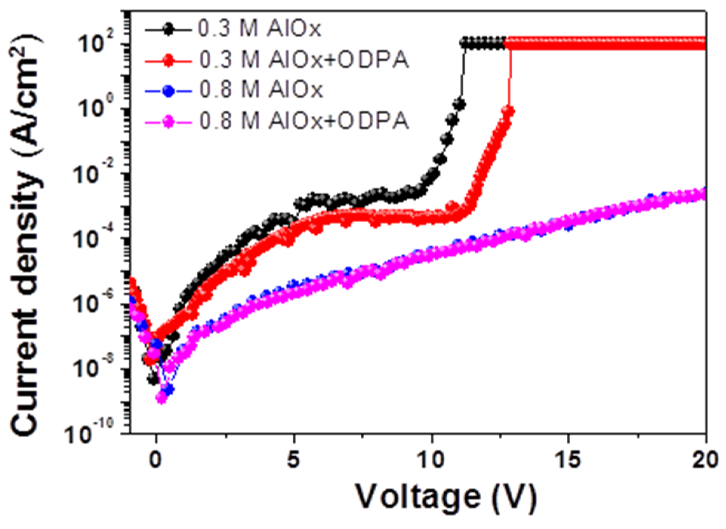
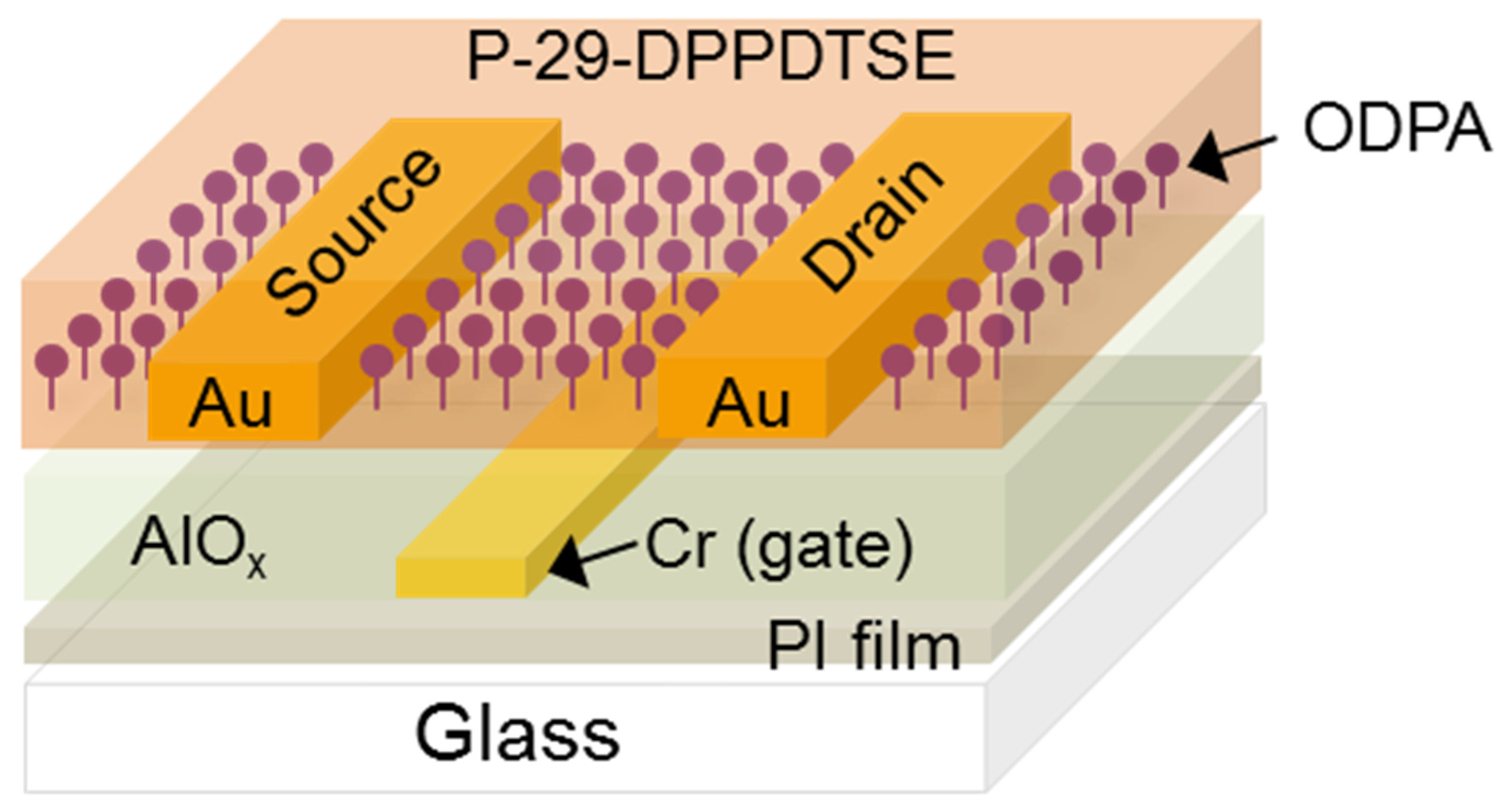
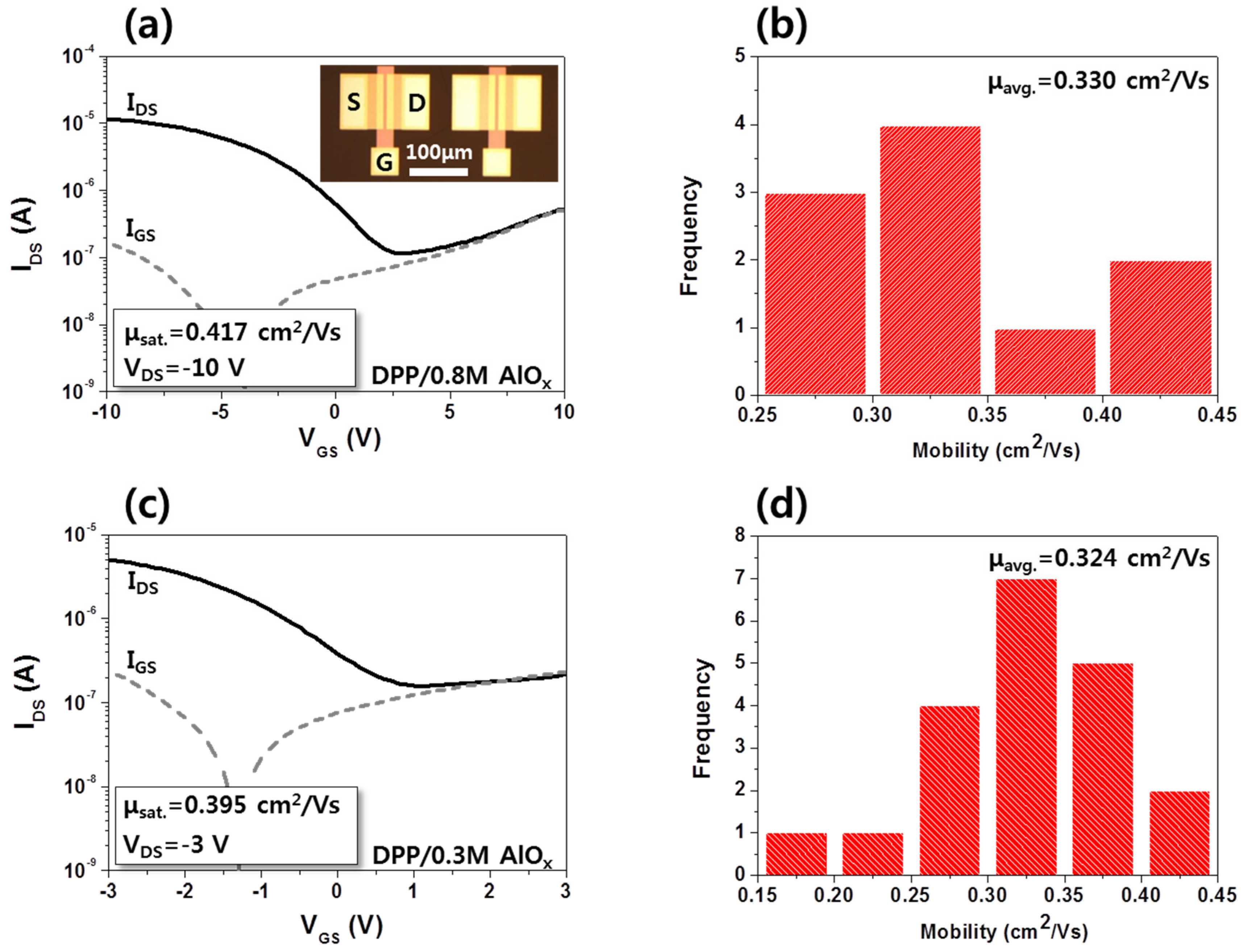
3. Results and Discussion

Among the various high-k metal oxides, AlOx was chosen for consideration in this study because of its relatively high k and wide bandgap, which correspond to a low turn-on voltage and low leakage current. Other high-k materials, such as ZrOx and YOx, could suffer from a relatively large leakage current due to their low conduction band offsets, although they offer a higher k value than AlOx [29,30,31]. Figure 1 displays the surface morphologies of the photochemically annealed AlOx dielectric layers before and after DUV annealing, for the different AlOx sol-gel concentrations of 0.3 and 0.8 M (hereafter referred to as 0.3- and 0.8-M AlOx, respectively). These two concentrations of AlOx represent the thin and thick film for use of gate dielectric layers, respectively. AFM analysis revealed that the as-deposited AlOx films exhibited a substantial decrease in RMS roughness after photochemical activation. Specifically, the initial RMS roughness values of 0.64 and 0.66 nm for the softbaked 0.3- and 0.8-M AlOx samples were reduced to 0.32 and 0.36 nm, respectively, following DUV annealing. Note that no obvious difference in AlOx surface roughness for the different sol-gel concentrations was found in this study. This can primarily be attributed to the densification and condensation of the AlOx precursors upon DUV irradiation, accompanied by the removal of organic species and solvents [24,25]. As a rough dielectric surface often leads to the deterioration of charge carrier mobility in semiconductors due to surface scattering, it is extremely important to keep the surface roughness of the dielectric layer as low as possible [18]. Additional ODPA organic molecules have been known to be effective in suppressing the leakage current of dielectric layer while enhancing the performance of OTFTs [22,32]. It should be also noted that no noticeable difference of root mean square (RMS) roughness was found from 0.3 and 0.8 M concentration of AlOx precursors. The final thicknesses of the 0.3- and 0.8-M AlOx dielectric layers were estimated to be approximately 13.5 and 48.2 nm, respectively (not shown). Additional ODPA organic molecules have been known to effectively suppress the leakage current of a dielectric layer while enhancing the performance of OTFTs [22,32], and additional SAM treatment appears to increase the total thickness of the dielectric layer by 2.2 nm; this value roughly corresponds to the ODPA molecule length [22,33]. For estimating the length of ODPA molecules, the step height measurement of AlOx film with and without ODPA treatment using AFM instrument was carried out following the patterning. As the as-deposited 0.8-M AlOx layer exceeded 180 nm in thickness, this suggests that DUV irradiation effectively causes the formation of dense metal–oxide films. Therefore, photochemical treatment of sol-gel precursors at medium-range temperatures (~150 °C) can also be used to fabricate OTFTs on a flexible substrate.
Areal capacitance measurement of the 0.3- and 0.8-M AlOx films was employed in order to investigate their performance as gate dielectric layers for low-voltage OTFTs. Figure 2a is a schematic diagram of the M-I-M device structure, while Figure 2b shows the capacitance vs. frequency characteristics of AlOx films with and without ODPA SAM treatment. The capacitance values of the photochemically annealed 0.3- and 0.8-M AlOx films at 100 Hz were 366 and 149 nF/cm2, respectively. The ODPA treatment reduced the capacitance of the 0.3-M AlOx film slightly, whereas no visible change was apparent in the case of the 0.8-M AlOx. This difference might be ascribed to the fact that the capacitance of the thicker 0.8-M AlOx film remains less sensitive to the thin molecule layer. The relatively stable capacitance at higher frequency implies the efficient removal of organic species within the films and also the formation of dense oxide films. Incomplete M-O-M bonding formation and organic residues often yield a noticeable decrease in areal capacitance at high frequency [34,35]. The relative dielectric constant of the photochemically annealed AlOx was estimated to be approximately 6.3, which is comparable to the values reported in the literature [36].
Figure 1. AFM surface scans of (a,b) softbaked and (c,d) DUV-annealed AlOx dielectric layers formed with 0.3- and 0.8-M AlOx sol-gel concentrations, respectively.
Materials 08 05352 g001
Figure 2. (a) Schematic illustration of metal–insulator–metal device structure and (b) capacitance vs. frequency characteristics of Au-AlOx/ODPA-Cr/glass devices used in this study.
Materials 08 05352 g002aMaterials 08 05352 g002b
The leakage current behavior of the photochemically annealed 0.8-M AlOx film under applied bias exhibited a stable dielectric property, as shown in Figure 3. Notably, no sudden electrical breakdown was observed for currents below 10−3 A/cm2 at a bias voltage of up to 15 V, which also indicates dense film formation due to the photochemical activation. For lower-operation-voltage OTFTs, a thinner dielectric layer with higher capacitance and an acceptable leakage current is always desired [17,22,37]. As stated previously, the 0.3-M AlOx yields a 13.5-nm thin high-k dielectric layer, thus favoring high capacitance. Here, the 0.3-M AlOx M-I-M devices seemed to retain a low leakage current up to almost 5-V applied bias, as shown in Figure 3. Therefore, the low-leakage-current behavior of thin AlOx dielectric films seems to be comparable to the values for high-temperature-annealed oxide gate dielectrics reported in the literature [34,36,38]. It can be understood that low-temperature photochemical activation enables the use of low thermal budget methods for sol-gel-derived oxide insulating layers. This suggests that photochemically annealed thin AlOx films can be used as high-capacitance dielectric layers to realize OTFTs with low operation voltages. Furthermore, ODPA SAM passivation lowers the leakage current density and increases the breakdown voltage to some extent [22,39].
Figure 3. Leakage current characteristics of Au-AlOx/ODPA-Cr/glass devices with 0.3- and 0.8-M AlOx sol-gel concentrations.
Materials 08 05352 g003
Using the fabricated AlOx films, high-performance P-29-DPPDTSE OTFTs were fabricated on a 3-μm thin PI/glass substrate using a bottom-gate and -contact electrode configuration, as shown in Figure 4. DUV-annealed 0.3- and 0.8-M AlOx dielectric layers were formed following patterning of the gate electrode. Figure 5a,b show the transfer characteristics and statistical distribution of the saturation mobility of the P-29-DPPDTSE OTFT with a 0.8-M AlOx gate dielectric layer. The inset of Figure 5a is an optical microscopy image of an OTFT with a 0.8-M AlOx dielectric layer. Note that no visual defects, such as cracking and inhomogeneity, are apparent. The average mobility of the P-29-DPPDTSE OTFT with a composite dielectrics of ODPA and 0.8 M AlOx layers was estimated to be as high as 0.330 cm2/Vs, while the current on/off ratio (Ion/Ioff) appeared to be approximately 2 × 10². Without SAM treatment on AlOx, we obtained much lower mobility of about 0.03 cm2/Vs, possibly due to less ordering in the semiconducting polymer films. The relatively low Ion/Ioff could be due to insufficient isolation of the high-performance organic layer. The flexible substrate made us difficult to physically isolate the high-performance semiconducting layer. A rigid substrate such as silicon allowed us to fabricate OTFTs with 5 × 10⁶ current on/off ratio. A histogram of the mobility distribution of these OTFTs is shown in Figure 5b, indicating the uniformity of the device performance. For the P-29-DPPDTSE OTFT with the 0.3-M AlOx film, the operation voltage was reduced to 3 V without the appearance of a significant gate leakage current or any device breakdown, as shown in Figure 5c. No significant device performance degradation was observed for this OTFT. In other words, the average mobility was as high as 0.324 cm2/Vs. There seems to be no obvious relation between the performance of OTFTs and thickness of dielectric layers. Slight difference of saturation mobility of OTFTs with 0.3- and 0.8-M AlOx implies that their surface properties appears quite similar, giving rise to similar level of molecular ordering within the semiconducting polymers. A uniform distribution was again obtained, as shown in Figure 5d. It should be noted that both OTFTs on the different flexible films demonstrated high charge carrier mobility of >0.3 cm2/Vs on average. Additional optimization of these devices through refinement of both the ODPA treatment and semiconductor processing conditions could further improve the observed device performance.
Figure 4. Schematic diagram of high-performance P-29-DPPDTSE polymer semiconductor device on a flexible PI film/glass substrate with DUV-annealed AlOx gate dielectric layers (not to scale).
Materials 08 05352 g004
Figure 5. (a,c) Transfer curves and (b,d) statistical distributions for saturation mobility of high-performance P-29-DPPDTSE polymer semiconductor devices on flexible PI film/glass substrates with 0.3- and 0.8-M AlOx sol-gel concentrations, respectively.
Materials 08 05352 g005

4. Conclusions

In conclusion, it was demonstrated that a high-performance low-operation-voltage P-29-DPPDTSE polymer semiconductor OTFT can be achieved using a photochemically activated AlOx gate dielectric layer. Additional ODPA SAM treatment enhances the leakage current characteristics of the AlOx film, while also improving the charge carrier mobility performance of the obtained OTFTs. Using a 0.3-M AlOx film, the fabricated P-29-DPPDTSE OTFT was successfully operated at a gate voltage lower than 3 V and exhibited a saturation mobility of ~0.3 cm2/Vs on a flexible PI film substrate. Therefore, the findings of this work indicate that photochemical activation of sol-gel precursors for use in dielectric materials constitutes a promising fabrication technique for solution-processable organic electronics with the capacity for low-voltage operation.

Acknowledgments

This work was partially supported by the Industrial Strategic Technology Development Program [10045145, Development of high performance (>70 cm2/Vs) chalcogenide TFT backplane and cadmium-free highly efficient (>30 cd/A) hybrid EL material/devices] funded by MOTIE/KEIT and by the Chung-Ang University Research Scholarship Grants in 2014.

Author Contributions

Jaekyun Kim, Chang Jun Park, and Gyeongmin Yi performed the experiments and the data analysis. Myung-Seok Choi helped in drafting the manuscript and in carrying out the data analysis and evaluation. Sung Kyu Park made the substantial contribution to the concept of experiments and was responsible for leading the project. All authors read and approve the final manuscript.

Conflicts of Interest

The authors declare no conflict of interest.

References

  1. Gelinck, G.H.; Huitema, H.E.A.; van Veenendaal, E.; Cantatore, E.; Schrijnemakers, L.; van der Putten, J.B.P.H.; Geuns, T.C.T.; Beenhakkers, M.; Giesbers, J.B.; Huisman, B.H.; et al. Flexible active-matrix displays and shift registers based on solution-processed organic transistors. Nat. Mater. 2004, 3, 106–110. [Google Scholar] [CrossRef] [PubMed]
  2. Klauk, H.; Zschieschang, U.; Pflaum, J.; Halik, M. Ultralow-power organic complementary circuits. Nature 2007, 445, 745–748. [Google Scholar] [CrossRef] [PubMed]
  3. Kane, M.G.; Campi, J.; Hammond, M.S.; Cuomo, F.P.; Greening, B.; Sheraw, C.D.; Nichols, J.A.; Gundlach, D.J.; Huang, J.R.; Kuo, C.C.; et al. Analog and digital circuits using organic thin-film transistors on polyester substrates. IEEE Electron Device Lett. 2000, 21, 534–536. [Google Scholar] [CrossRef]
  4. Mabeck, J.T.; Malliaras, G.G. Chemical and biological sensors based on organic thin-film transistors. Anal. Bioanal. Chem. 2006, 384, 343–353. [Google Scholar] [CrossRef] [PubMed]
  5. Liao, C.; Yan, F. Organic semiconductors in organic thin-film transistor-based chemical and biological sensors. Polym. Rev. 2013, 53, 352–406. [Google Scholar] [CrossRef]
  6. Dodabalapur, A. Organic and polymer transistors for electronics. Mater. Today 2006, 9, 24–30. [Google Scholar] [CrossRef]
  7. Giri, G.; Verploegen, E.; Mannsfeld, S.C.B.; Atahan-Evrenk, S.; Kim, D.H.; Lee, S.Y.; Becerril, A.; Aspuru-Guzik, A.; Toney, M.F.; Bao, Z. Tuning charge transport in solution-sheared organic semiconductors using lattice strain. Nature 2011, 480, 504–508. [Google Scholar] [CrossRef] [PubMed]
  8. Minemawari, H.; Yamada, T.; Matsui, H.; Tsutsumi, J.; Haas, S.; Chiba, R.; Kumai, R.; Hasegawa, T. Inkjet printing of single-crystal films. Nature 2011, 475, 364–367. [Google Scholar] [CrossRef] [PubMed]
  9. Kim, Y.-H.; Yoo, B.; Anthony, J.E.; Park, S.K. Controlled deposition of a high-performance small-molecule organic single-crystal transistor array by direct ink-jet printing. Adv. Mater. 2012, 24, 497–502. [Google Scholar] [CrossRef] [PubMed]
  10. Yuan, Y.; Giri, G.; Ayzner, A.L.; Zoombelt, A.P.; Mannsfeld, S.C.B.; Chen, J.; Nordlund, D.; Toney, M.F.; Huang, J.; Bao, Z. Ultra-high mobility transparent organic thin film transistors grown by an off-centre spin-coating method. Nat. Commun. 2014, 5, 1–8. [Google Scholar] [CrossRef] [PubMed]
  11. Li, Y.; Singh, S.P.; Sonar, P. A high mobility p-type DPP-thieno[3,2-b]thiophene copolymer for organic thin-film transistors. Adv. Mater. 2010, 22, 4862–4866. [Google Scholar] [CrossRef] [PubMed]
  12. Yan, H.; Chen, Z.; Zheng, Y.; Newman, C.; Quinn, J.R.; Dötz, F.; Kastler, M.; Facchetti, A. A high-mobility electron-transporting polymer for printed transistors. Nature 2009, 457, 679–686. [Google Scholar] [CrossRef] [PubMed]
  13. Zhang, X.; Richter, L.J.; DeLongchamp, D.M.; Kline, R.J.; Hammond, M.R.; McCulloch, I.; Heeney, M.; Ashraf, R.S.; Smith, J.N.; Anthopoulos, T.D.; Toney, M.F. Molecular packing of high-mobility diketo pyrrolo-pyrrole polymer semiconductors with branched alkyl side chains. J. Am. Chem. Soc. 2011, 133, 15073–15084. [Google Scholar] [CrossRef] [PubMed]
  14. Kang, I.; Yun, H.; Chung, D.S.; Kwon, S.; Kim, Y. Record high hole mobility in polymer semiconductors via side chain engineering. J. Am. Chem. Soc. 2013, 135, 14896–14899. [Google Scholar] [CrossRef] [PubMed]
  15. Noriega, R.; Rivnay, J.; Vandewal, K.; Koch, F.P.V.; Stingelin, N.; Smith, P.; Toney, M.F.; Salleo, A. A general relationship between disorder, aggregation and charge transport in conjugated polymers. Nat. Mater. 2013, 12, 1038–1044. [Google Scholar] [CrossRef] [PubMed]
  16. Yoon, M.-H.; Yan, H.; Facchetti, A.; Marks, T.J. Low-voltage organic field-effect transistors and inverters enabled by ultrathin cross-linked polymers as gate dielectrics. J. Am. Chem. Soc. 2005, 127, 10388–10395. [Google Scholar] [CrossRef] [PubMed]
  17. Pal, B.N.; Dhar, B.M.; See, K.C.; Katz, H.E. Solution-deposited sodium beta-alumina gate dielectrics for low-voltage and transparent field-effect transistors. Nat. Mater. 2009, 8, 898–903. [Google Scholar] [CrossRef] [PubMed]
  18. Facchetti, A.; Yoon, M.-H.; Marks, T.J. Gate dielectrics for organic field-effect transistors: New opportunities for organic electronics. Adv. Mater. 2005, 17, 1705–1725. [Google Scholar] [CrossRef]
  19. Cho, J.H.; Lee, J.; He, Y.; Kim, B.S.; Lodge, T.P.; Frisbie, C.D. High-capacitance ion gel gate dielectrics with faster polarization response times for organic thin film transistors. Adv. Mater. 2008, 20, 686–690. [Google Scholar] [CrossRef]
  20. Kim, J.; Jang, J.; Kim, K.; Kim, H.; Kim, S.H.; Park, C.E. The origin of excellent gate-bias stress stability in organic field-effect transistors employing fluorinated-polymer gate dielectrics. Adv. Mater. 2014, 7241–7246. [Google Scholar] [CrossRef] [PubMed]
  21. Yoon, W.-J.; Berger, P.R. Atomic layer deposited HfO2 gate dielectrics for low-voltage operating, high-performance poly-(3-hexythiophene) organic thin-film transistors. Org. Electron. 2010, 11, 1719–1722. [Google Scholar] [CrossRef]
  22. Park, Y.M.; Daniel, J.; Heeney, M.; Salleo, A. Room-temperature fabrication of ultrathin oxide gate dielectrics for low-voltage operation of organic field-effect transistors. Adv. Mater. 2011, 23, 971–974. [Google Scholar] [CrossRef] [PubMed]
  23. Beaulieu, M.R.; Baral, J.K.; Hendricks, N.R.; Tang, Y.; Briseño, A.L.; Watkins, J.J. Solution processable high dielectric constant nanocomposites based on ZrO2 nanoparticles for flexible organic transistors. ACS Appl. Mater. Interfaces 2013, 5, 13096–13103. [Google Scholar] [CrossRef] [PubMed]
  24. Wang, H.; Sun, T.; Xu, W.; Xie, F.; Ye, L.; Xiao, Y.; Wang, Y.; Chen, J.; Xu, J. Low-temperature facile solution-processed gate dielectric for combustion derived oxide thin film transistors. RSC Adv. 2014, 4, 54729–54739. [Google Scholar] [CrossRef]
  25. Braquinho, R.; Salgueiro, D.; Santos, L.; Braquinha, P.; Pereira, L.; Martins, R.; Fortunato, E. Aqueous combustion synthesis of aluminum oxide thin films and application as gate dielectric in GZTO solution-based TFTs. ACS Appl. Mater. Interfaces 2014, 6, 19592–19599. [Google Scholar] [CrossRef] [PubMed]
  26. Xu, W.; Wang, H.; Xie, F.; Chen, J.; Cao, H.; Xu, J.-B. Facile and environmentally friendly solution-processed aluminum oxide dielectric for low-temperature, high-performance oxide thin-film transistors. ACS Appl. Mater. Interfaces 2015, 7, 5803–5810. [Google Scholar] [CrossRef] [PubMed]
  27. Jo, J.-W.; Kim, J.; Kim, K.-T.; Kang, J.-G.; Kim, M.-G.; Kim, K.-H.; Ko, H.; Kim, Y.-H.; Park, S.K. Highly stable and imperceptible electronics utilizing photoactivated heterogeneous sol-gel metal-oxide dielectrics and semiconductors. Adv. Mater. 2015, 27, 1182–1188. [Google Scholar] [CrossRef] [PubMed]
  28. Park, S.; Kim, K.-H.; Jo, J.-W.; Sung, S.; Kim, K.-T.; Lee, W.-J.; Kim, J.; Kim, H.J.; Yi, G.-R.; Kim, Y.-H.; Yoon, M.-H.; Park, S.K. In-depth studies on rapid photochemical activation of various sol-gel metal oxide films for flexible transparent electronics. Adv. Funct. Mater. 2015, 25, 2807–2815. [Google Scholar] [CrossRef]
  29. Waggoner, T.; Triska, J.; Hoshino, K.; Wager, J.F.; Conley, J.F. Zirconium oxide-aluminum oxide nanolaminate gate dielectrics for amorphous oxide semiconductor thin-film transistors. J. Vac. Sci. Technol. B: Microelectron. Nanometer Struct. 2011, 29. [Google Scholar] [CrossRef]
  30. Yang, W.; Song, K.; Jung, Y.; Jeong, S.; Moon, J. Solution-deposited Zr-doped AlOx gate dielectrics enabling high-performance flexible transparent thin film transistors. J. Mater. Chem. C 2013, 1. [Google Scholar] [CrossRef]
  31. Song, K.; Yang, W.; Jung, Y.; Jeong, S.; Moon, J. A solution-processed yttrium oxide gate insulator for high-performance all-solution-processed fully transparent thin film transistors. J. Mater. Chem. 2012, 22. [Google Scholar] [CrossRef]
  32. Park, Y.M.; Desai, A.; Salleo, A.; Jimison, L. Solution-processable zirconium oxide gate dielectrics for flexible organic field effect transistors operated at low voltages. Chem. Mater. 2013, 25, 2571–2579. [Google Scholar] [CrossRef]
  33. Ma, H.; Acton, O.; Hutchins, D.O.; Cernetic, N.; Jen, A.K.-Y. Multifunctional phosphonic acid self-assembled monolayers on metal oxides as dielectrics, interface modification layers and semiconductors for low-voltage high-performance organic field-effect transistors. Phys. Chem. Chem. Phys. 2012, 14, 14110–14126. [Google Scholar] [CrossRef] [PubMed]
  34. Xu, W.; Wang, H.; Ye, L.; Xu, J. The role of solution-processed high-κ gate dielectrics in electrical performance of oxide thin-film transistors. J. Mater. Chem. C 2014, 2. [Google Scholar] [CrossRef]
  35. Park, J.H.; Kim, K.; Yoo, Y.B.; Park, S.Y.; Lim, K.-H.; Lee, K.H.; Baik, H.K.; Kim, Y.S. Water adsorption effects of nitrate ion coordinated Al2O3 dielectric for high performance metal-oxide thin-film transistor. J. Mater. Chem. C 2013, 1. [Google Scholar] [CrossRef]
  36. Avis, C.; Jang, J. High-performance solution processed oxide TFT with aluminum oxide gate dielectric fabricated by a sol–gel method. J. Mater. Chem. 2011, 21. [Google Scholar] [CrossRef]
  37. Xu, X.; Cui, Q.; Jin, Y.; Guo, X. Low-voltage zinc oxide thin-film transistors with solution-processed channel and dielectric layers below 150 °C. Appl. Phys. Lett. 2012, 101. [Google Scholar] [CrossRef]
  38. Meyers, S.T.; Anderson, J.T.; Hong, D.; Hung, C.M.; Wager, J.F.; Keszler, D.A.; State, O.; Uni, V.; Hall, G.; Cor, V. Solution-processed aluminum oxide phosphate thin-film dielectrics. Chem. Mater. 2007, 19, 4023–4029. [Google Scholar] [CrossRef]
  39. Xia, G.; Wang, S.; Zhao, X.; Zhou, L. High-performance low-voltage organic transistor memories with room-temperature solution-processed hybrid nanolayer dielectrics. J. Mater. Chem. C 2013, 1. [Google Scholar] [CrossRef]

