
A Survey on Memory Subsystems for Deep Neural Network Accelerators


Electrical and Computer Engineering Department, Toronto Metropolitan University, 350 Victoria St, Toronto, ON M5B 2K3, Canada
*
Author to whom correspondence should be addressed.
†
These authors contributed equally to this work.
Future Internet 2022, 14(5), 146; https://doi.org/10.3390/fi14050146
Submission received: 15 March 2022
/
Revised: 4 May 2022
/
Accepted: 5 May 2022
/
Published: 10 May 2022
(This article belongs to the Topic Big Data and Artificial Intelligence)
Abstract
:From self-driving cars to detecting cancer, the applications of modern artificial intelligence (AI) rely primarily on deep neural networks (DNNs). Given raw sensory data, DNNs are able to extract high-level features after the network has been trained using statistical learning. However, due to the massive amounts of parallel processing in computations, the memory wall largely affects the performance. Thus, a review of the different memory architectures applied in DNN accelerators would prove beneficial. While the existing surveys only address DNN accelerators in general, this paper investigates novel advancements in efficient memory organizations and design methodologies in the DNN accelerator. First, an overview of the various memory architectures used in DNN accelerators will be provided, followed by a discussion of memory organizations on non-ASIC DNN accelerators. Furthermore, flexible memory systems incorporating an adaptable DNN computation will be explored. Lastly, an analysis of emerging memory technologies will be conducted. The reader, through this article, will: 1—gain the ability to analyze various proposed memory architectures; 2—discern various DNN accelerators with different memory designs; 3—become familiar with the trade-offs associated with memory organizations; and 4—become familiar with proposed new memory systems for modern DNN accelerators to solve the memory wall and other mentioned current issues.
1. Introduction
Deep neural networks (DNNs) have great potential and offer a multitude of benefits to solve new problems. DNNs are employed in many various domains; for instance, computer vision, image classification, computer prediction, and recognizing patterns prediction. In correspondence with DNN application growth, there is an increase in the demand for energy-efficient hardware architectures. This is a result of the large amount of parallel processing required to compute massive data sets. The communication and storage requirements needed by DNNs creates resistance on the path towards high power efficiency and performance.
In order to use a DNN to make accurate predictions, the DNN model must first be created and tuned using a set of training data. This is the first step in using a DNN and is called the training phase. The next phase, called the inference phase, involves the use of a trained model to make accurate predictions about the input data.
These two phases, though both related to the processing of data through a DNN, have key differences to consider. In the training phase, the goal is to minimize the time required for the output to converge to a certain accuracy, which improves the throughput of the system. Contrastingly, the inference phase is not as concerned with accuracy, but with latency and throughput. As a result, it is a prevalent practice to forgo accuracy in favor of increased throughput or decreased latency [1,2]. Furthermore, the two phases have different memory requirements. Unlike inference, where only the last layer of activations is stored, training requires almost all the activations of each layer so gradients can be computed in the back-propagation flow. Lastly, to achieve higher throughput, the training implementation exponentially increases in order to access numerous clusters and nodes [3].
The MAC operations represent the main arithmetic functions in processing DNNs. Each MAC contains three memory reads and one write. Memory is read for various tasks such as partial sum, fmap activation, and filter weights, and data is written to update the partial sum. The three memory accesses can, in the worst-case scenario, travel across the large energy toll/cost off-chip DRAM and this can significantly hamper energy efficiency and throughput. As a result, reducing memory access latency is imperative to the performance of the DNN, which motivates the research regarding different memory techniques.
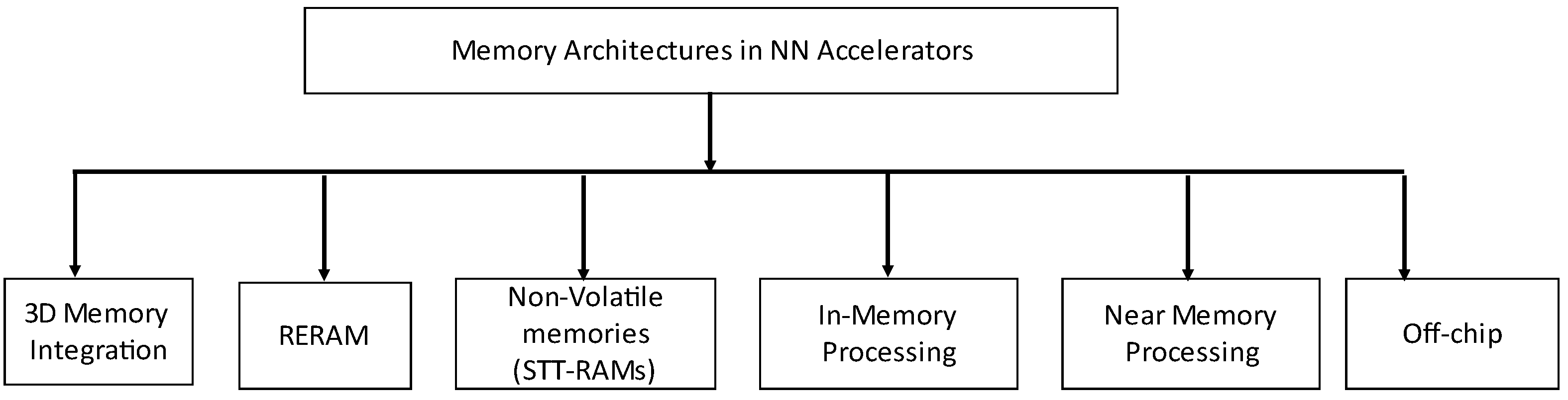
Considering that the further development of neural networks (NNs) is causing an increase in their size and complexity, it is critical that the efficiency and execution of NN accelerators possess the ability to sustain comparable growth. Expansion in the number and size of layers may cause the memory subsystems to exhibit a case of a bottleneck behavior in the NN accelerators. New memory architectures, for instance 3D memory [4,5,6,7,8,9,10,11,12], near memory [13,14,15,16,17,18], and in-memory processing [19], nonvolatile memories (NVMs) [20], and ReRAM [21,22,23,24,25,26,27,28,29], etc., have brought about an upheaval of performance in DNN computing.
Advancements in technology have allowed for new techniques to improve efficiency such as 3D memory. Compared to 2D memory, 3D memory has the capability of greatly improving bandwidth and energy efficiency. Given the recent advancement of through-silicon-vias (TSVs); 3D memory has the ability to be implemented by placing DRAM dice upon the logic chip. This can significantly cause memory access latency to decrease [30]. Considering the benefits, prospective NN accelerator designs can take cognizance of and plausibly utilize various 3D memory architectures [4,5,6,7,8,9,10,11,12].
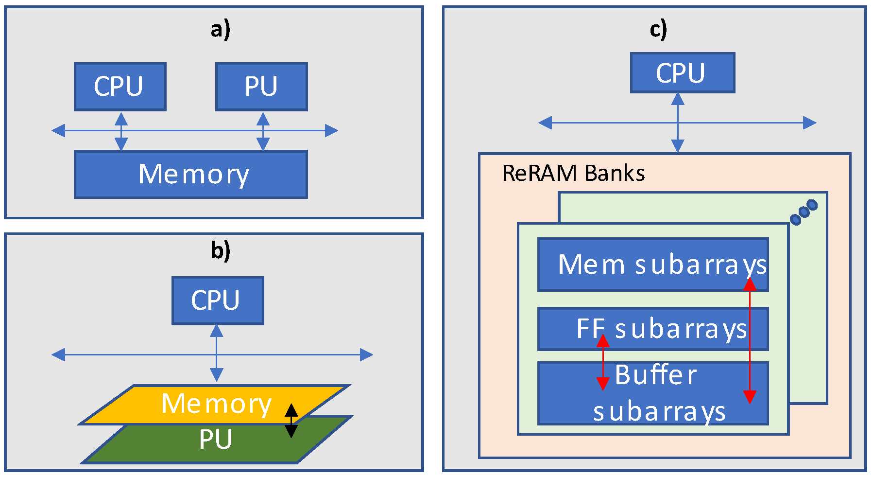
In-memory computing also offers an optimistic alternative to the memory wall challenge. These forms of processing, computation, and memory are integrated using novel memory technologies to bypass costly off-chip storage data transfers and PEs.
Given that some growing memory technologies, for example PCM [31], STT-RAM [30], ReRAM [31], and other examples of nonvolatile memories (NVMs) [20] can process arithmetic and logic operations along with reserving data, all have been explored extensively to accelerate applications such as graph processing [23,29], complex computing [30], and DNNs [1,2].
In summary, we will discuss different memory designs for DNN operation depending on the application and the goal of the design. Though other existing surveys report on DNN accelerators in overview, this article will provide an analysis of the various memory architectures used in DNN accelerators depending upon the many possible design scenarios.
This study is designed to assess the hypothesis that designing an energy-efficient memory architecture will improve the power consumption and performance of DNN accelerators significantly.
The main contributions of this article are highlighted below:
- (1)
- Accentuate the memory portion of DNN accelerator’s architecture including the processing element (PE) design.
- (2)
- Assess the DNN execution under various memory structures depending upon a multitude of design goals and applications.
- (3)
- Further notes for exploratory directions in regards to the future of DNN design after investigating the present-day models extensively.
Figure 1 shows the layout of this article.
Section 2 depicts the Preferred Reporting Items for Systematic reviews and Meta-Analyses (PRISMA) statement for the selection of articles to carry out the survey. Section 3 discusses the different 3D memory architectures in DNN accelerators and attempts to expound the various design compensations The fourth segment describes ReRAM as an emerging memory technology in DNN accelerators’ memory systems. Nonvolatile memories such as STT-RAMs and the other emerging memory technologies used in DNN accelerators’ memory systems are described in Section 5. Section 6 discusses the in-memory processing technology used in DNN accelerators’ memory systems and examines the performance impact depending on numerous parameters. Segment 7 reports other innovative memory technology, referred to as near-memory processing, used in DNN accelerators in order to achieve optimal execution of DNN operations. Segment 8 describes three off-chip memory architectures in DNN accelerators. In Section 9 the memory architecture for DNN accelerators is summarized, and ultimately the paper is concluded in Section 10.
2. PRISMA Methodology
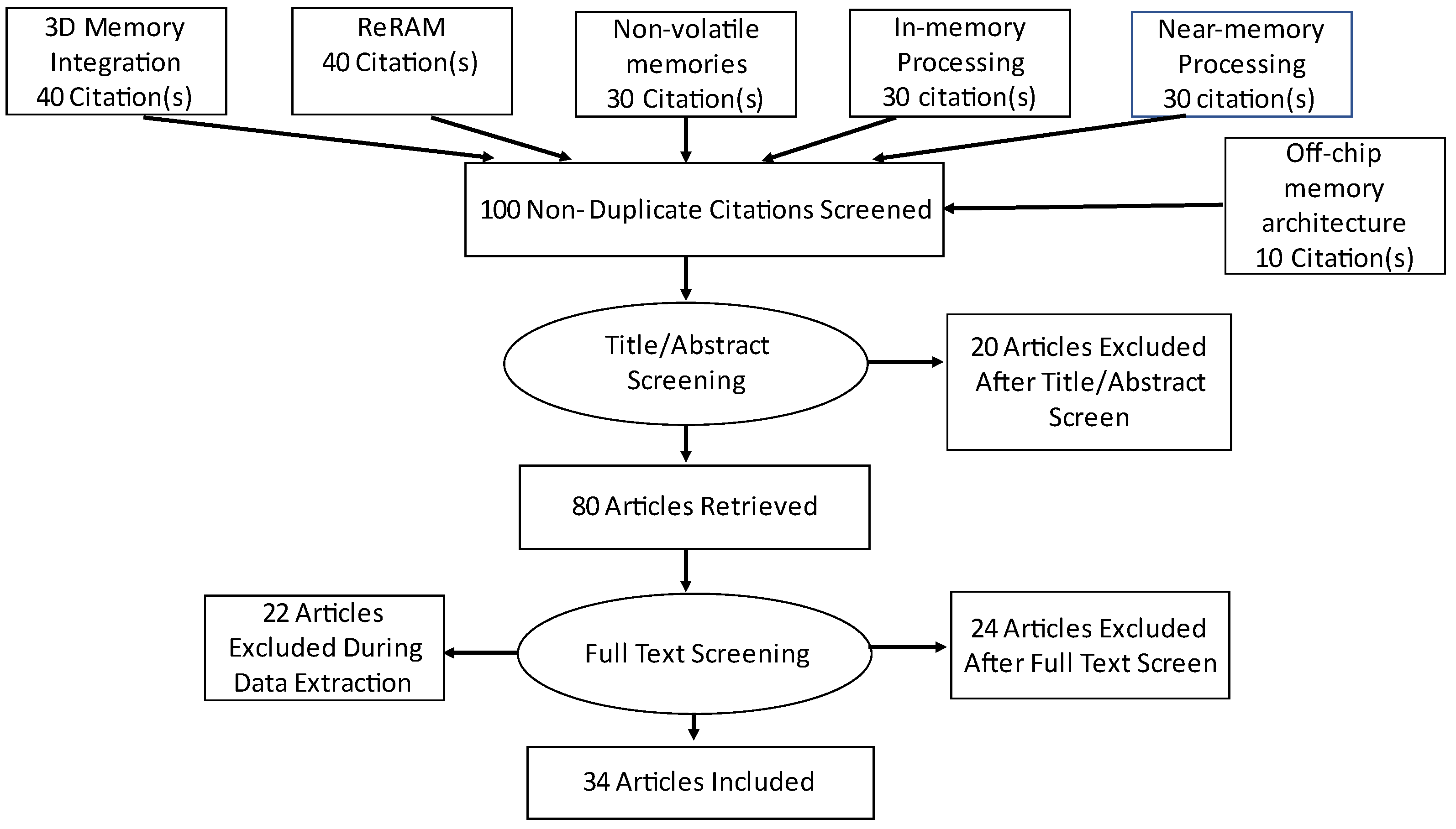
The cited papers have been selected on the basis of different memory architectures used in DNN accelerators. Figure 2 describes the paper selection methodology as per PRISMA statement. Several papers on 3D memory, ReRAM, nonvolatile memories, in-memory processing, near-memory processing and off-chip memory architectures have been screened for the survey.
3. 3D Memory Integration
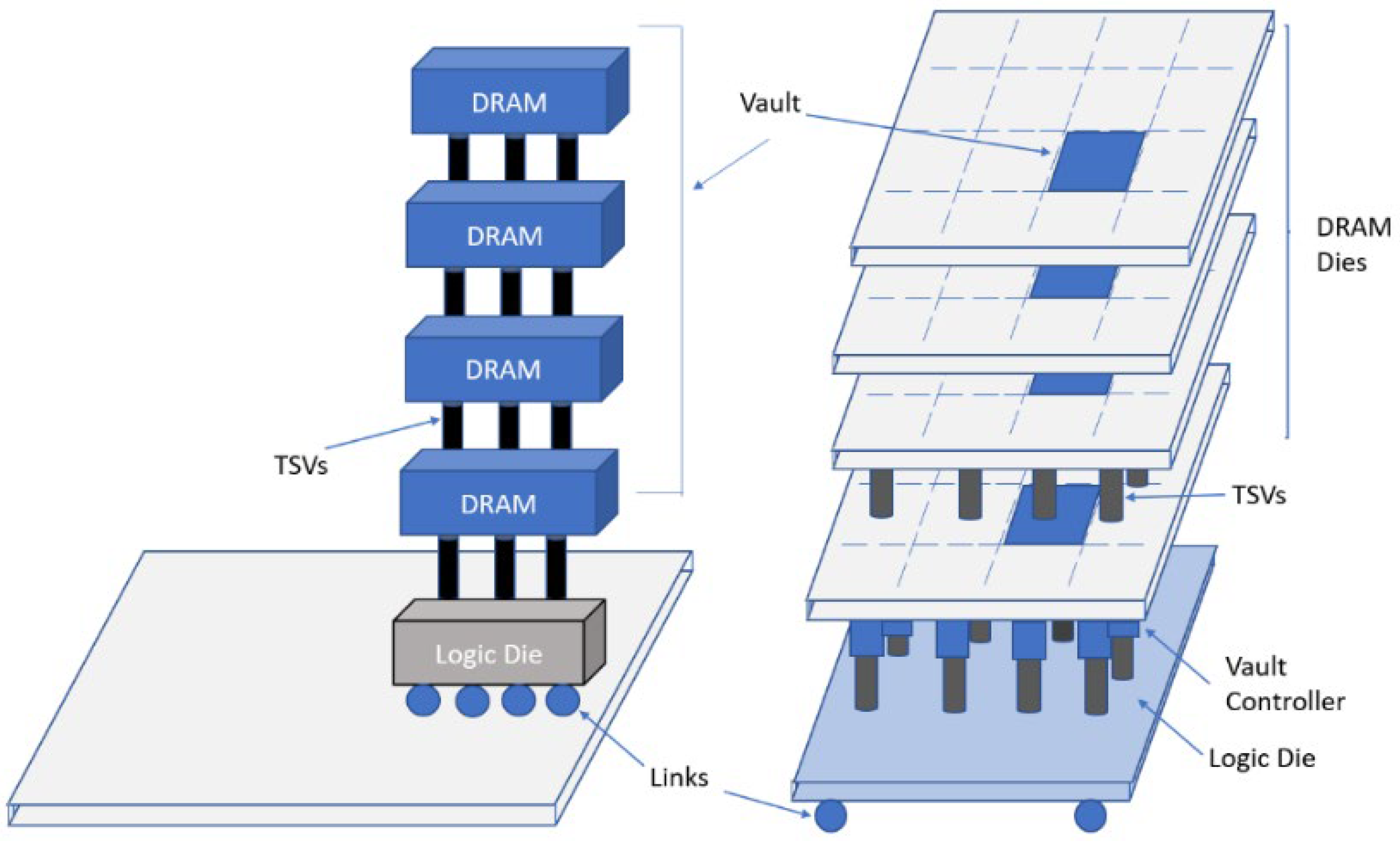
In order to integrate computational layers inside a three-dimensional topology of a memory package possessing very high levels of density, the hybrid memory cube (HMC) is a new concept introduced in [4]. DRAM dice are layered upon a logic die vertically in the HMC. The HMC offers an efficient near-data processing with respect to its large memory bandwidth and capacity, in addition to low latency.
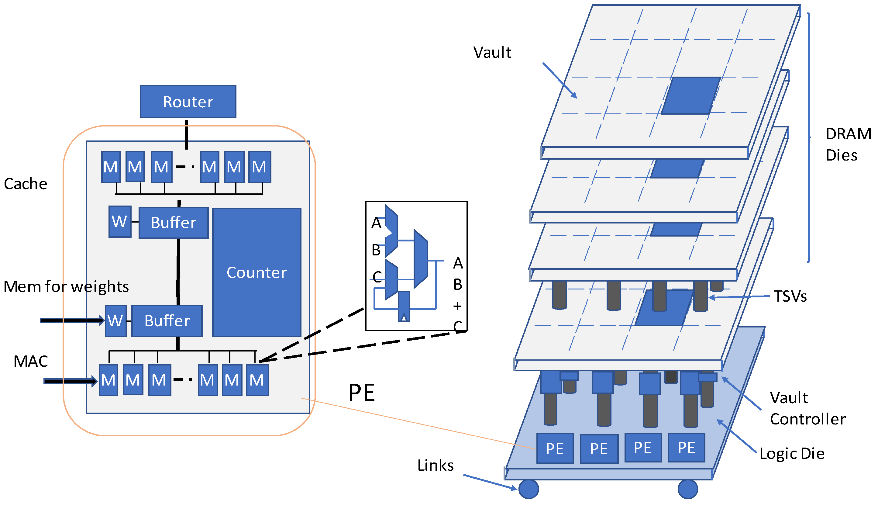
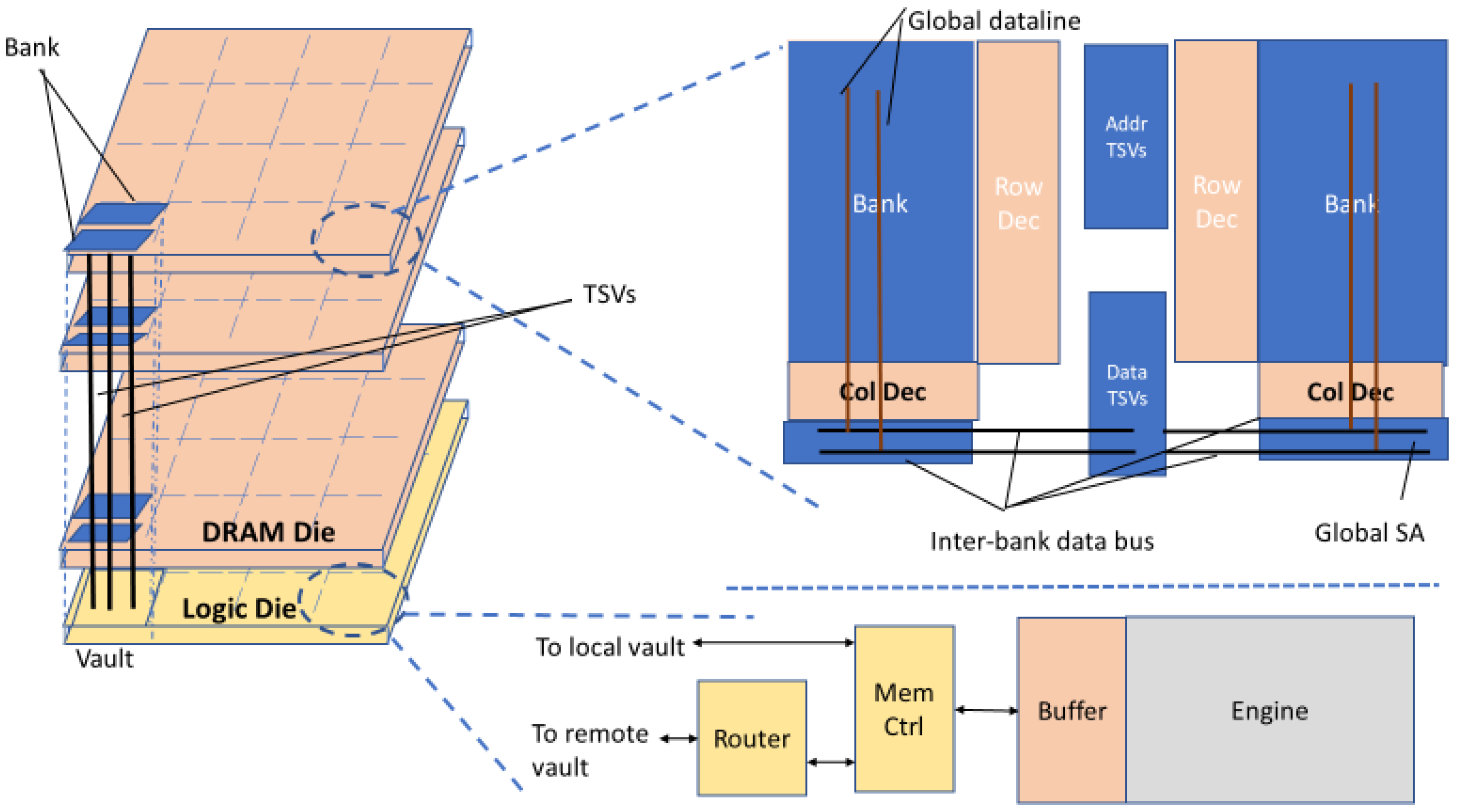
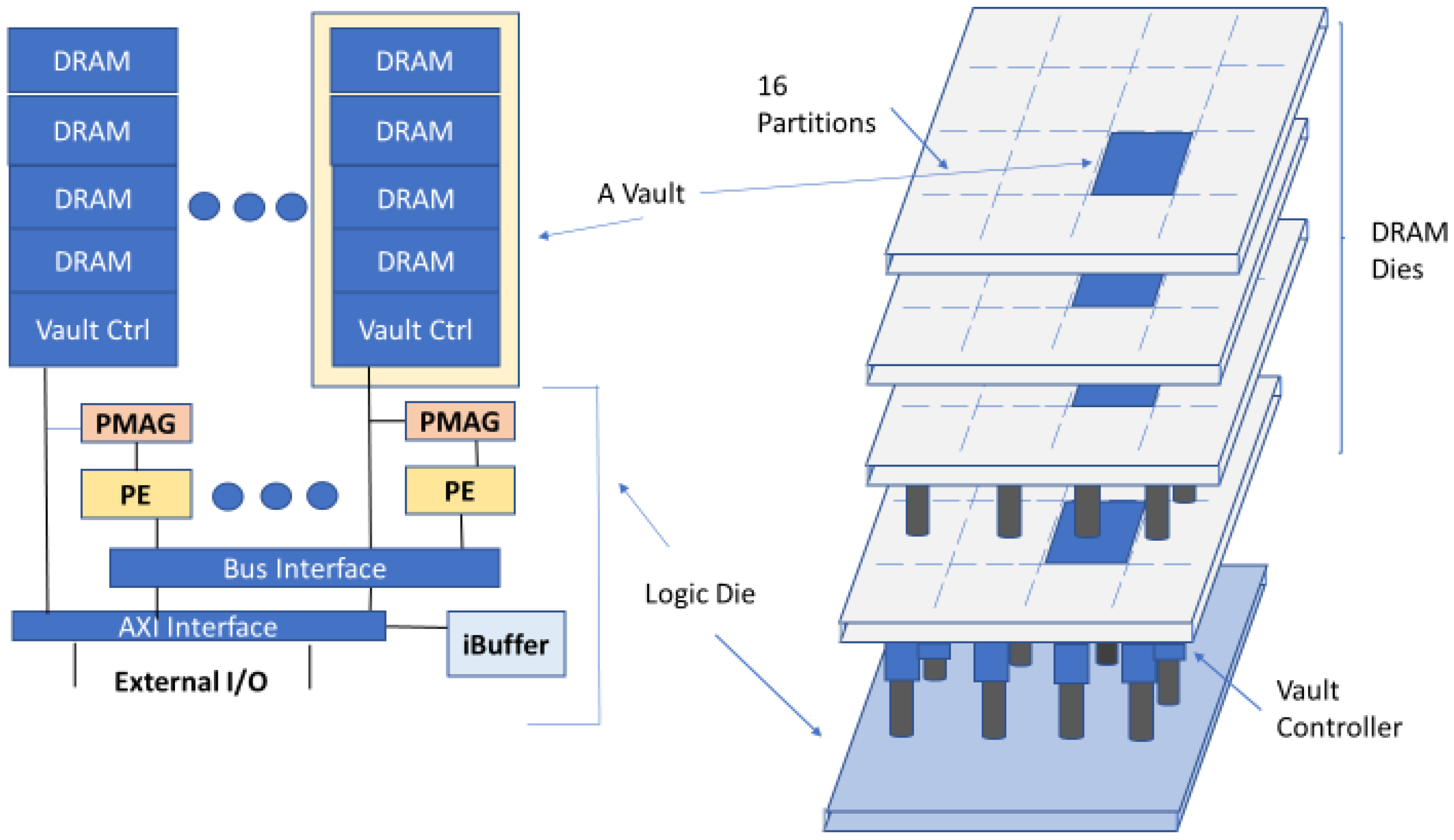
In the proposed HMC-based accelerator, named Neurocube, in [4], there is a logic die in the lowest layer and DRAM layers stacked on it, shown in Figure 3. The logic die in the lowest layer includes logic and computation components. As illustrated in Figure 3, the implementation of data storage for each PE is achieved by the DRAM dies in the vault. Since every vault possesses its own vault controller in the logic layer, the PEs can access multiple vaults in parallel.
HMC in the Neurocube accelerator has 16 vaults. As demonstrated in Figure 3 every vault is considered to be a subsystem, consisting of a router, and stacked DRAM dice. PEs perform multiply–accumulate (MAC) operations. Routers perform data transfer between the DRAM and logic layers. A source vault has the ability to transmit data packets to a target vault via the routers.
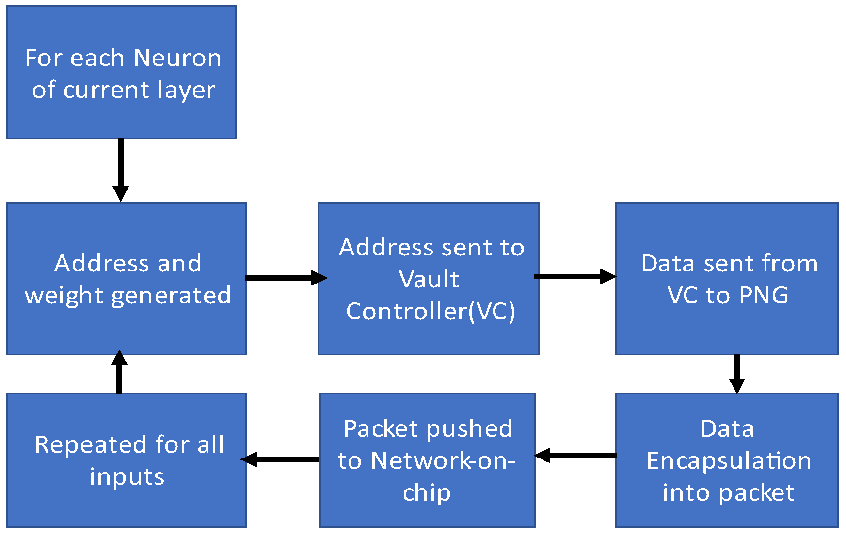
Neurocube programs the implementation of a single layer of an NN individually. Figure 4 examines the operation of a PNG, the key component in memory-centric neural computing in the accelerator, for each layer. The important mission of the PNG is to generate the weights and addresses of the neurons residing in the previous layer in the memory.
In addition to Neurocube, which is based on the HMC concept, TETRIS [5] is the other DNN accelerator based on the HMC.
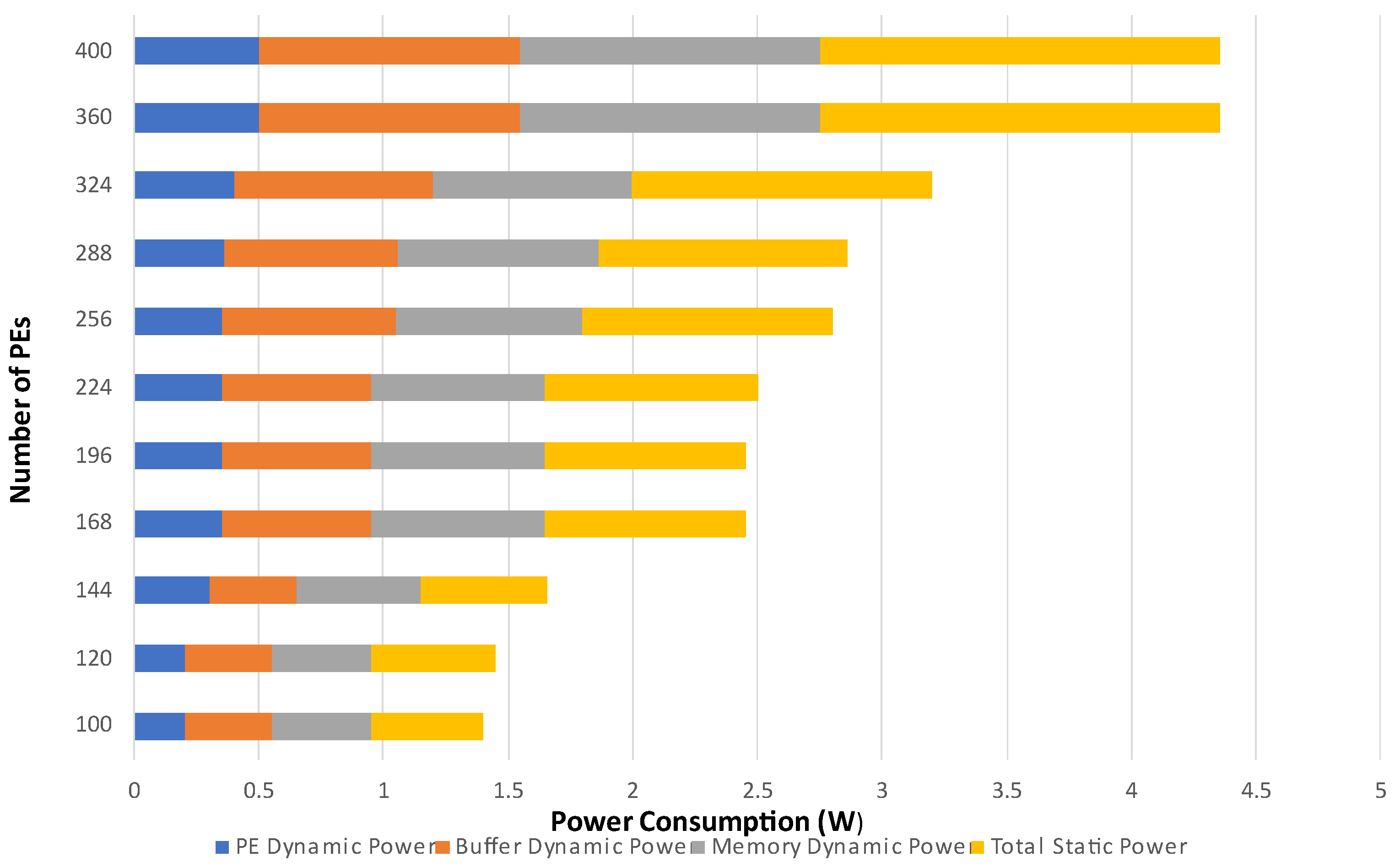
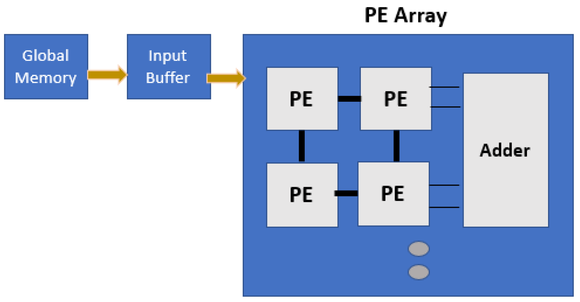
The performance of NN accelerators is limited by off-chip main memory and on-chip buffers. Although sizable on-chip SRAM buffers amounts in higher memory bandwidths, and DRAM access is also reduced, it also leads to a significant amount of power consumption (Figure 5). The 3D memory technology promises an efficient memory system for the NN accelerator.
DRAM memory dice are integrated vertically over the logic layer as a single package. This improves the bandwidth and lowers the access energy significantly. In order to completely utilize 3D memory benefits, there are certain challenges that are required to be addressed. Firstly, 3D memory technology allows different use of smaller on-chip memory buffers. Secondly, 3D technology gives the opportunity to decide where the computations will be carried out. Some operations can be moved close to memory locations. Thirdly, there is a wide scope to frame new approaches for dataflow scheduling of NN computations. Last but not least, an efficient partitioning scheme is required for highly parallelized 3D memory stacks.
Addressing the above stated challenges in [5], the scalability of neural networks is improved by the proposed TETRIS architecture in which the hardware includes 3D stacking of memory with processing elements. In addition to this, for the software side, an analytical representation is developed for optimized data flow schedules. At the hardware level, more area is utilized in processing elements in addition to minor area utilization with respect to SRAM buffers.
In the proposed TETRIS architecture, the HMC stack is alienated into 16 32-bit vaults. TSVs get utilized by the vault channel bus in order to connect to the DRAM memory dice to base logic die. This results in two banks per vault in each DRAM die (Figure 6). Two-dimensional mesh network is incorporated for the NN accelerator. All processing elements share a global buffer for storage and reuse of data from memory. In this manner, significant bandwidth of memory is saved, and performance is improved. In-memory allocation of the computation is carried out using DRAM die accumulation and bank accumulation, which improves computational efficiency of the accelerator. A hybrid partitioning scheme of NN computations in the parallel 3D stack system is also presented.
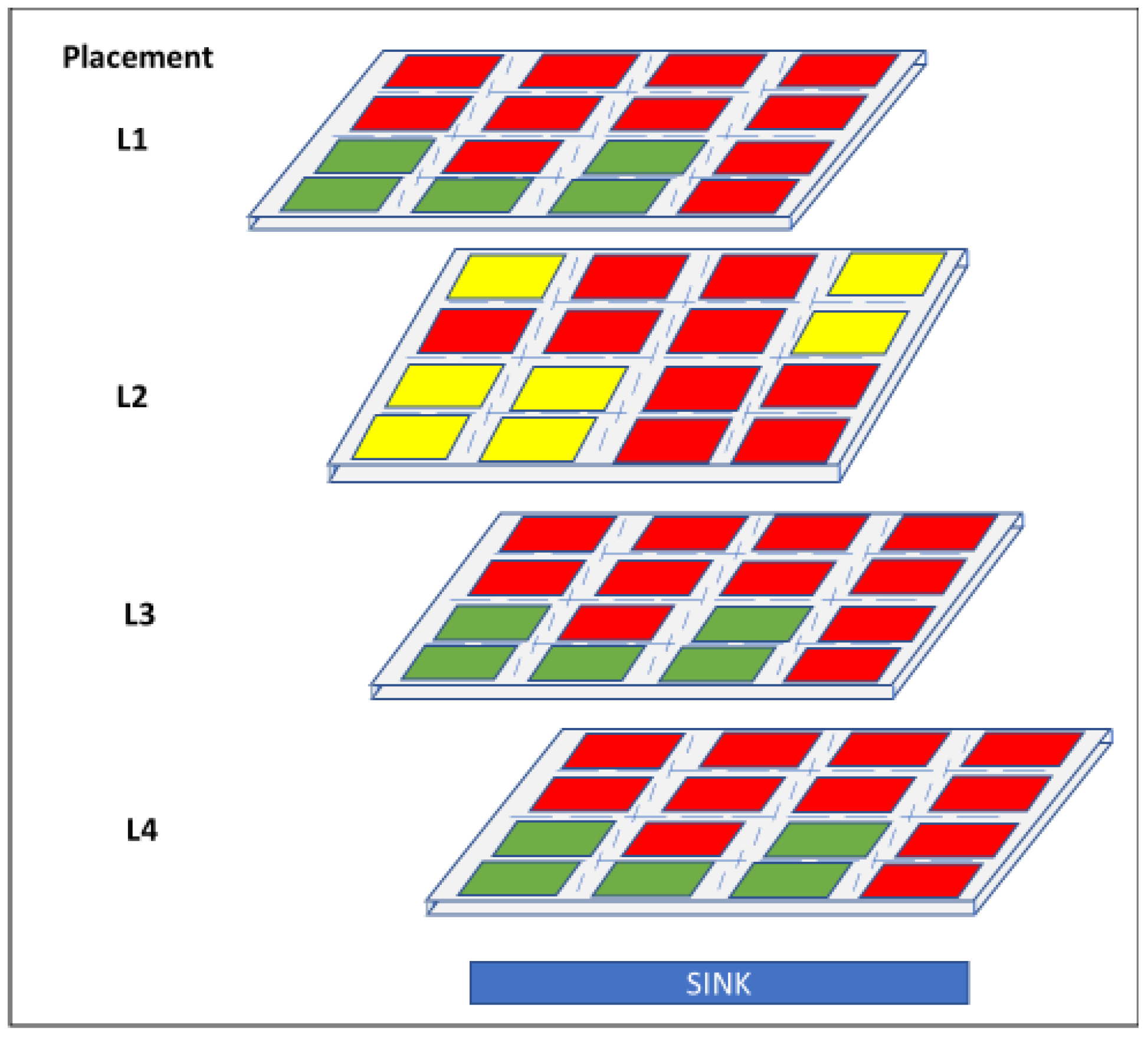
Joardar et al. [6] have proposed a designing technique for 3D heterogeneous manycore platforms for DNN applications using an (ML) established multiobjective optimization (MOO) method. In this case, the MOO method places last-level cache (LLC) banks, CPU, and GPU units in order to optimally minimize the access latency of the CPU memory and maximize the throughput of the GPU network. A multiobjective optimization (MOO) issue has been proposed for the optimally heterogenous placement in DNN-based applications. Figure 7 shows a result of the optimal placement by the presented ML-based MOO technique.
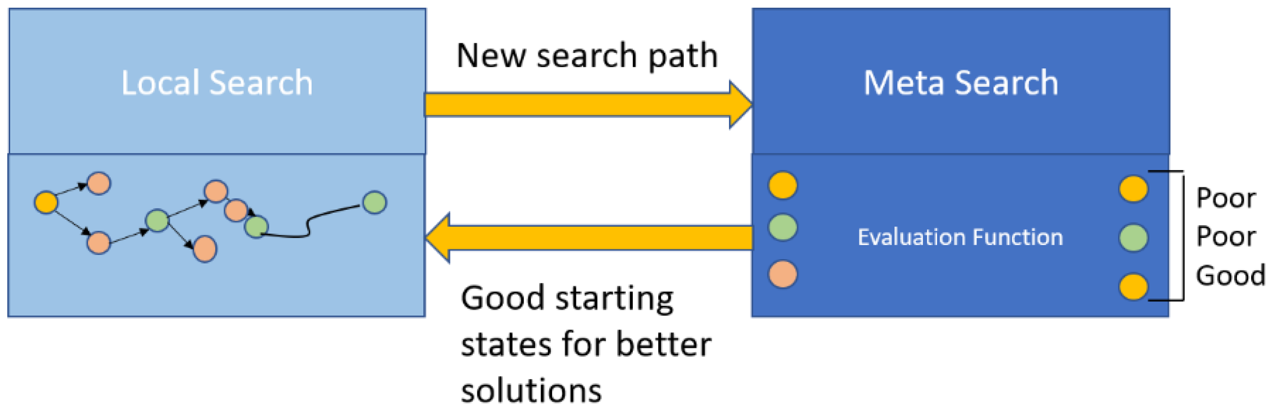
As illustrated in Figure 8, the ML-based MOO method includes two search methods in order to find an optimal placement. They are local search and meta search. In the former methodology, local search, also known as a greedy search, is an optimized path along which a series of adjacent states are traversed for an optimal solution to satisfy the given objectives. On the other hand, in the learning phase (meta search), a regression forest technique is used to find the highest-quality initial state for the next local search iteration.
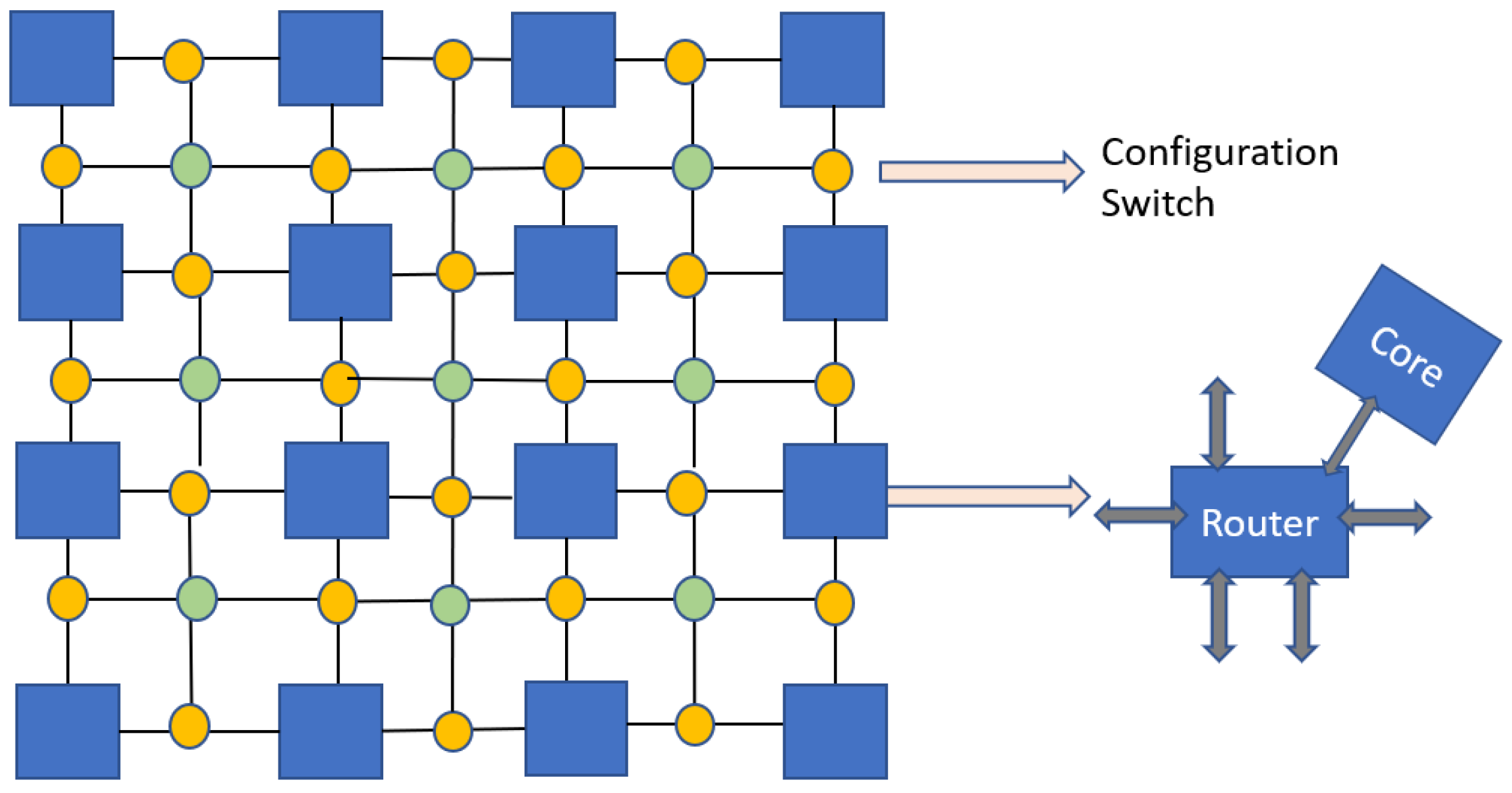
In order to overcome the challenges of basic bus topology in neural networks, networks-on-ships (NoCs) emerge as a promising candidate. In Figure 9, a customizable architecture for NoCs in terms of three-dimensional memory logic is presented [7]. The processing elements are arranged in the form of clusters, which are linked in an adjustable network. Such a network can adjust the inter-cluster configuration in order to carry out connectivity between memory and processing elements. The memory layers, stacked above the logic layer, are divided into several panels. A memory channel is formed by each pair of vertically adjacent memory and logic.
The prime advantage of this architecture is that the inter-router connections can be reconfigured through configuration switches (represented in Figure 9). With such a topology, several networks-on-chips can be built by managing cluster size, number of clusters, and number of switches between two clusters. Reconfigurability of the network promises improved power efficiency than conventional mesh topologies.
In the design flow proposed in [7], firstly the neural network is divided across NoCs using layer-wise division. Then, the divided neurons are mapped on NoC nodes. The grouping is done in such a manner such that adjacent divisions are grouped together and same layer neurons are combined in each cluster. Furthermore, a mapping algorithm is utilized to map the division groups and clusters. Figure 10 shows the mapping of a cluster of neurons onto a vault. Finally, inter-cluster links are configured through configuration switches and routers.
Another innovative DNN architecture called RAPIDNN is proposed in [8], in which neuron to memory transformation is carried out to enhance the performance of the DNN network. This memory design is purely based on digital computations. Therefore, analog-to-digital conversion and vice versa are not required in this design. Hence, area and power overhead are significantly decreased.
Figure 11 shows the outline of RAPIDNN structure. In this model, first the computation flow of DNN is analyzed. Then, the DNN operations are encoded. Furthermore, clustering algorithms are utilized to find parameters processed in each neuron. The key characteristic of this model is that the continuous functions as multiplication and activation can be considered as stepwise functions with minimal DNN inference.
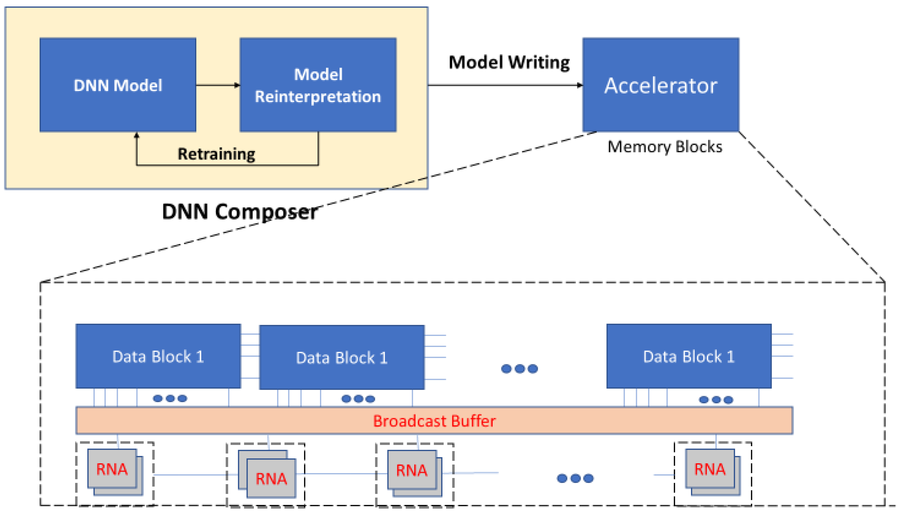
The RAPIDNN architecture proposed in [8] maps all the functionalities into the memory block. It utilizes a single level memristor device, rather than multilevel memristors. The RAPIDNN network consists of two modules: DNN composer (software) and accelerator (hardware) as depicted in Figure 11. DNN composer creates a table of each neural network operation, which can be stored in accelerator memory blocks. This sequence of operations is shown in Figure 12.
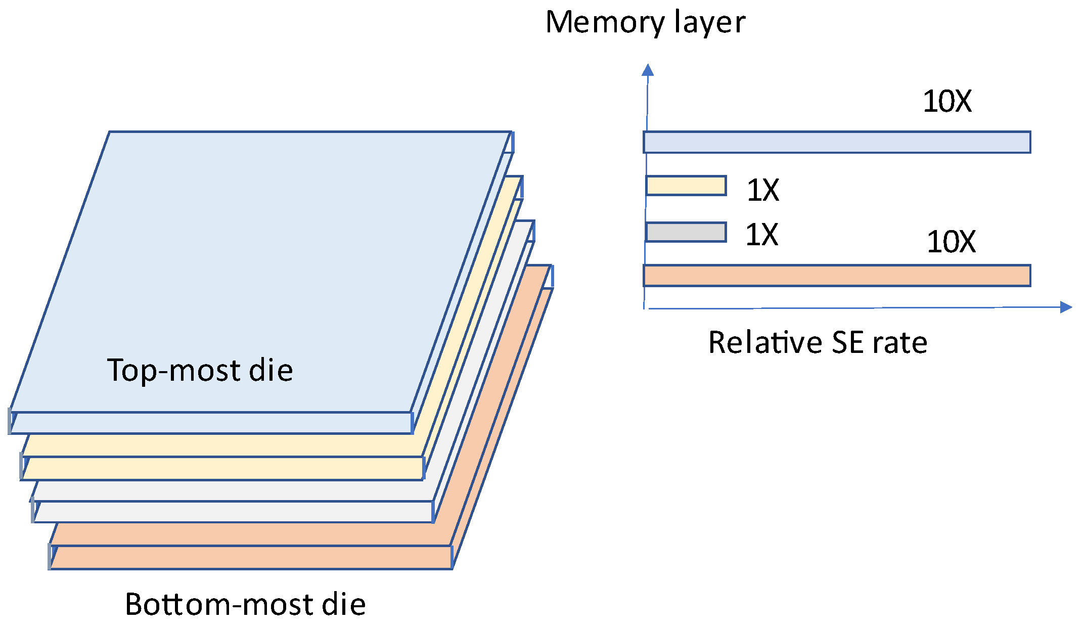
In [9], a reliability improvement scheme in a DNN accelerator with 3D memory integration has been proposed. High bandwidth memory (HBM) is a new concept introduced in [9]. In 3D-stacked memories, there is a different soft error rate (SER) in every layer, unlike planar memories. Since from the top of the package material alpha particles rise up, the top-most layer shows a higher SER than the remaining layers. In addition, the bottom-most layer also shows a high rate of SER due to the heat released from the interposer and logic units. As shown in Figure 13, the uppermost and lower-most layers show 10 times higher SER in comparison with the remaining layers.
Authors in [9] mention that DNN possesses very accurate results in areas such as image classification. The majority of computations in DNNs are produced in the hidden layer—consisting of weighted filters.
For every layer stored in the stacked DRAM dice, a frequently applied input feature map is able to extract the corresponding output feature map. In this process, the same weight filter, stored in the stacked DRAM dice, is read from numerous interactions by the memory. If faults are injected into weights, a duplicate fault effect can be caused by repetitive memory accesses. Authors in [9] find that all the weights in AlexNet are below than 1. The 29th and 30th bits of all the weights are 0 and 1 when they are expressed in 32-bit floating point. Two following cases show that flipping just one bit has a high impact on accuracy.
- ▪ Case-1: flipping the 29th bit (1→0) for 500 weights in each layer of DNN.
- ▪ Case-2: flipping the 30th bit (0→1) for 5 weights in each layer of DNN.
Therefore, faults on weights, and everything stored in memory layers, create abnormality in operations. Kim et al. in [9] shows that designing fault-tolerant DNN accelerators for reaching high accuracy levels is a topic that should be taken into consideration.
Deeptrain [11] presents a novel architecture using the 3D stacking processing-in-memory (PIM) paradigm. It applies to the hybrid memory cube (HMC) concept for accelerating training and inference [11]. Deeptrain integrates a logic layer in the lower layer and high-bandwidth DRAM layers in upper layers for eliminating off-chip DRAM accesses. Deeptrain is for DNN training using an embedded platform, yet it does not possess the quality of back propagation of pooling layers and weight updates by the DNN. An overview of Deeptrain architecture has been displayed in Figure 14.
Every programmable memory address generator (PMAG) is equipped with a vault. This PMAG unit is a key component in Deeptrain. PMAG realizes different data flows in Deeptrain based on a state machine. PMAG maps various data (gradients, parameters, and inputs) to individual vaults. PMAG couples partitioning as well as data mapping along with the bus communication fabric. PMAG can be configured in regards to numerous computational kernels in the training phase.
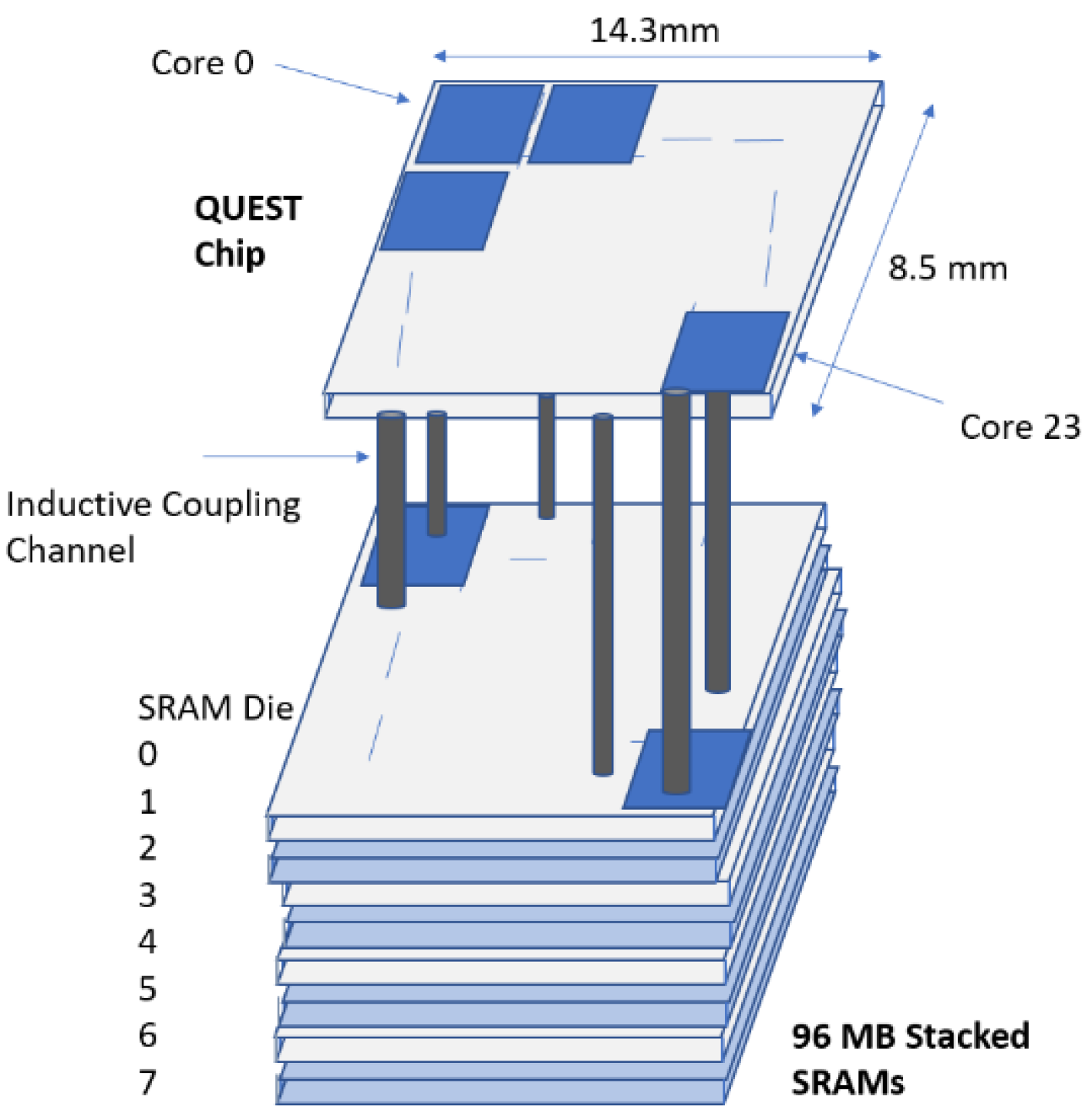
In recent studies, 3D memory stacking-based architectures for DNN have been introduced. These structures utilize DRAM stacking over the processing elements. 3D stacking has been witnessed to offer numerous advantages; however, the DRAM latency poses a difficult problem. In addition to this, optimization based on algorithms have resulted in an improper DRAM architecture. In order to overcome these challenges, SRAM-based 3D memory stacking is viewed as a promising solution. Such a log-quantized architecture called QUEST has been proposed in [12]. The design structure for this architecture has been depicted in Figure 15.
Improved efficiency, reduced area, and higher memory bandwidth are the favorable attributes of log quantization. The multiplications are replaced by additions in log quantization; therefore, it offers reduced area computations compared with linear quantization. In this architecture, reconfigurable arrays with bit-serial data lines instead of parallel data paths have been adopted. Therefore, different bit-precision configurations are well-advocated. Also, this methodology allows the utilization of distinct kinds of layers for neural networks with the aid of a unified hardware. Numerous configurations for neural networks are therefore effectively mapped. In this architecture, 3D SRAM has been used as external memory with inductive coupling technique. Stacking of SRAM instead of DRAM offers reduced memory access time.
Summary and Discussion
This section analyzes different papers discussing efficient 3D memory architectures in DNN accelerators. The literature reflects that the hybrid memory cube (HMC) concept develops as a prominent possibility for the DNN accelerator memory architectures where a compute layer is stacked within numerous memory layers. In addition to HMC, reconfigurable network-on-chip architecture is also presented, which implements inter-cluster topology to carry out data transfer between memory and processing elements. Some works utilize stacking of SRAM instead of DRAM and promise reduced access times. Though 3D stacking offers heterogeneous integration, density and power overloads need to be addressed as some challenges in this area.
4. ReRAM Technology
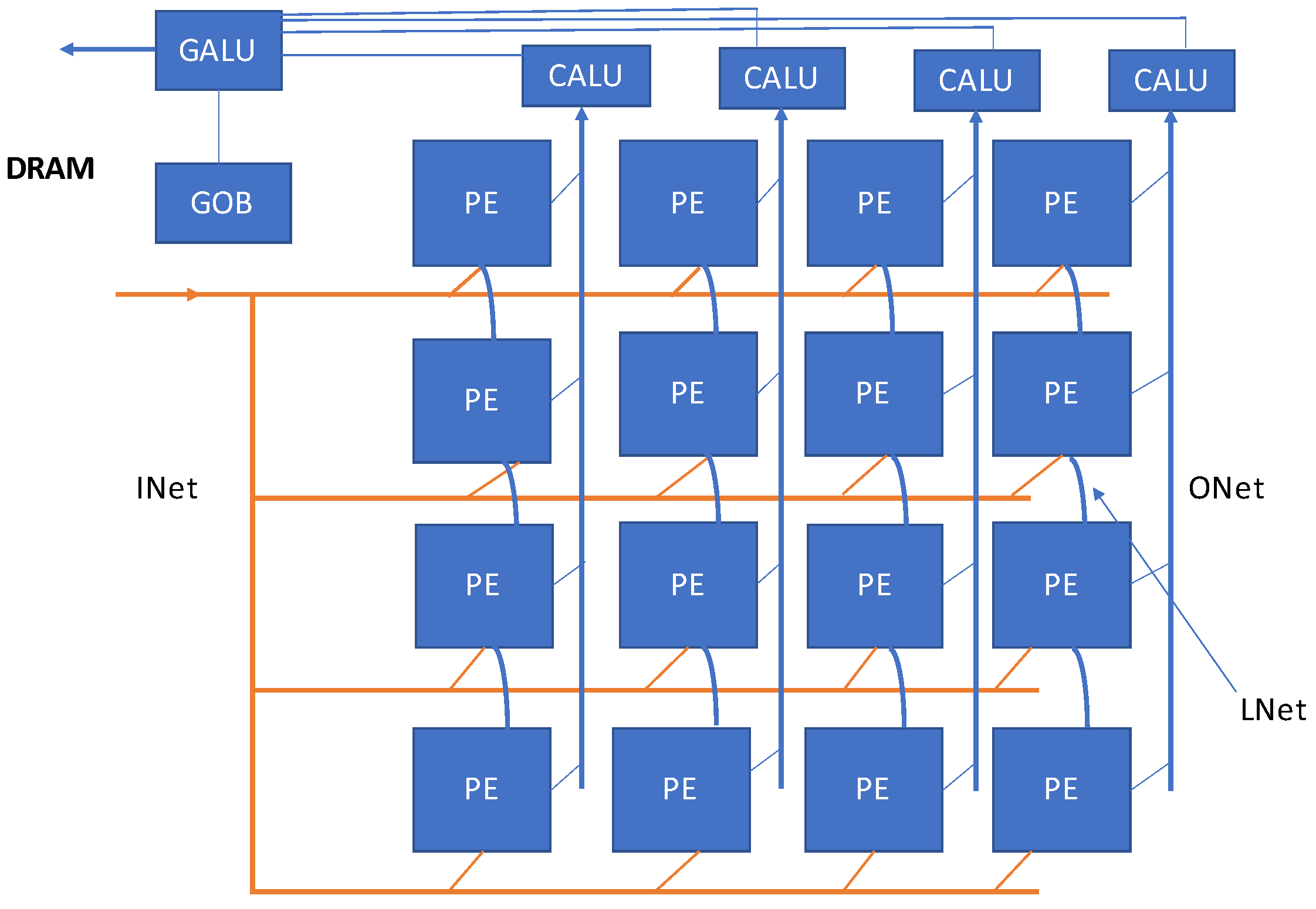
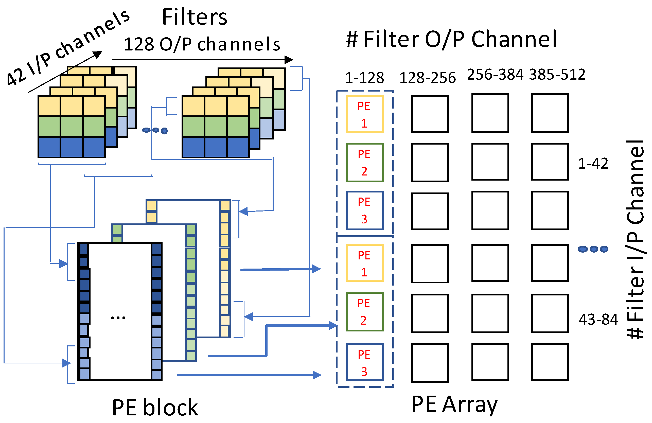
Another promising design of DNN accelerator is based on processing-in-memory implemented using ReRAM technology. In resistive random-access memory (ReRAM), the computations are performed by storage of neural network filters into the ReRAM cells. One such ReRAM-based DNN accelerator is proposed in [21]. The presented architecture ‘atomlayer’ carries out atomic layer computations, thereby promising to overcome the pipeline issues witnessed in previous designs. Execution of one neural network at a time reduces latency and on-chip buffer overhead significantly. The atom layer compromises an array of processing elements, ALU tree, and global output buffer along with the on-chip network. The presented atom-layer architecture is shown in Figure 16.
Each processing element contains rotating crossbars, peripheral devices such as DACs/ADCs, and four buffers. The crossbars are utilized to provide storage for filters and computation of convolution. The atom-layer architecture makes use of a data-reuse technique in which row-disjoint filter mapping allocates multiple hardware levels from the data reuse hierarchy levels as shown in Figure 17.
Chi et al. [21] propose PRIME, a neuromorphic accelerator using resistive random-access memory (ReRAM). PRIME using memristors instead of the DRAM main memory to perform neural computations in memory. PRIME uses a 256 by 256 memristor array size, which can be used for either a 4-bit multilevel cell computation or a 1-bit single-level cell repository. Due to the pipeline organizations, PRIME cannot support training efficiently. In this neuromorphic accelerator, stable ReRAM cross bars are applied to store the weights as well as perform in-situ analog dot product operations for processing in memory (PIM).
A set of peripheral circuits have been designed in PRIME to configure a malleable PIM structure with regard to the ReRAM main memory. This proposed PIM allows the use of arrays in terms of scratch pads dot product engines as well as arrays specifically for DNN workloads.
Positive and negative connections are both supported by PRIME, but the input vectors have to be unsigned. Another shortcoming of the PRIME is lossy computations regarding the dot product due to the precision in ADC not always matching the accuracy of the computed dot product. In [21], computation of the product in a 4-bit weight and 3-bit input has been shown, the same as the limited precision shown in mixed signal circuits in this work. In addition, the conversion overhead between the ADC and DAC should be also examined in the overall cost. This is most notable when the weights are trained in the digital domain. Figure 18 demonstrates a trend from traditional shared memory technology to PRIME, a new 3D PIM based on ReRAM technology.
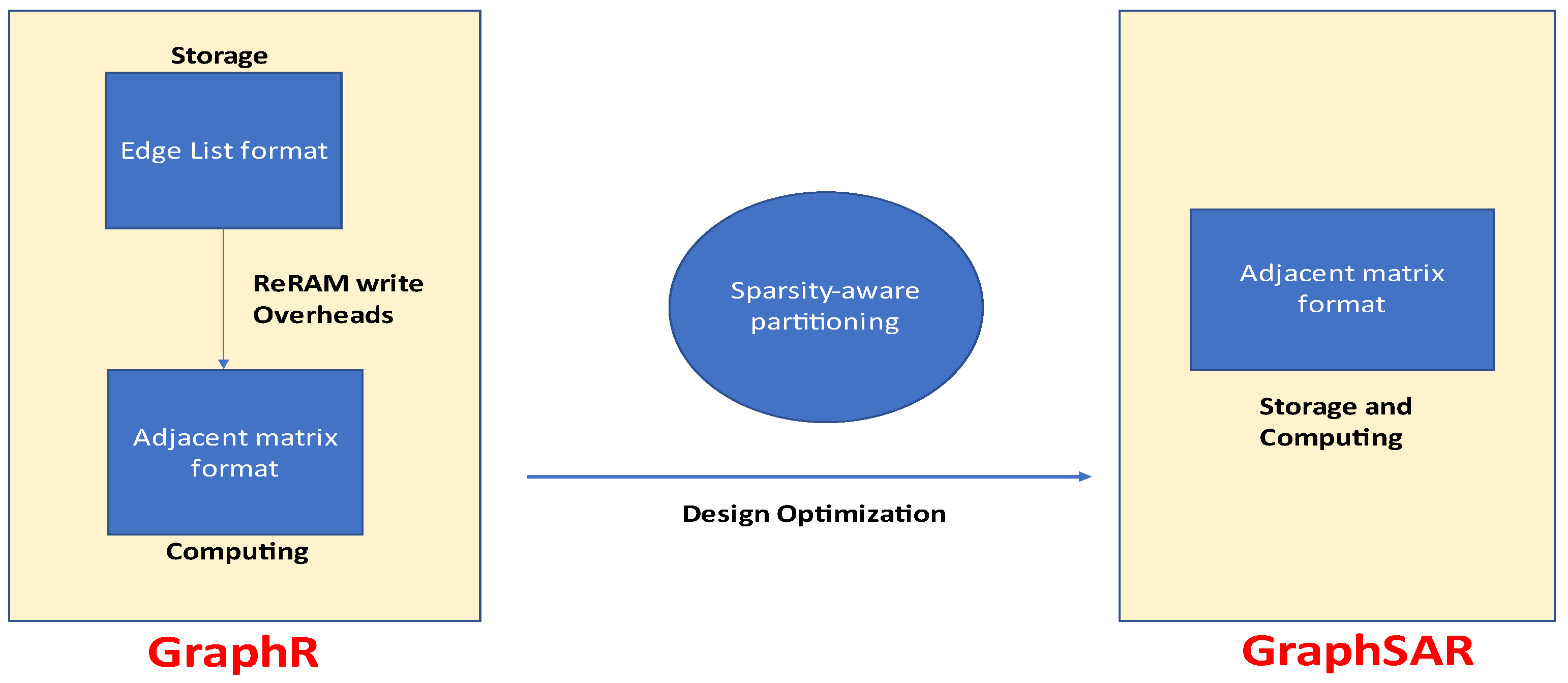
ReRAM and crossbar networks based on it, have immense ability for graph processing. However, the separate storage and computation of edges contributed to higher power consumption and longer latencies. Overcoming this limitation of graph processing, a large-scale graphical processing accelerator based on ReRAM called GraphSAR is proposed in [23]. GraphSAR utilizes processing-in-memory technique to eliminate writing overheads to ReRAM crossbars. The computations are carried out directly in the memory. Also, memory space wastage is controlled by further division of low-density subgraphs.
Figure 19 shows the comparison of GraphSAR with a previous design, GraphR. GraphSAR supports direct processing of edges in the memory itself where they are placed. In such a manner, less energy is consumed. Also, the latency of putting edge values into the computational units is reduced considerably. In addition to this, sparsity-aware partitioning of subgraphs limits memory space overhead.
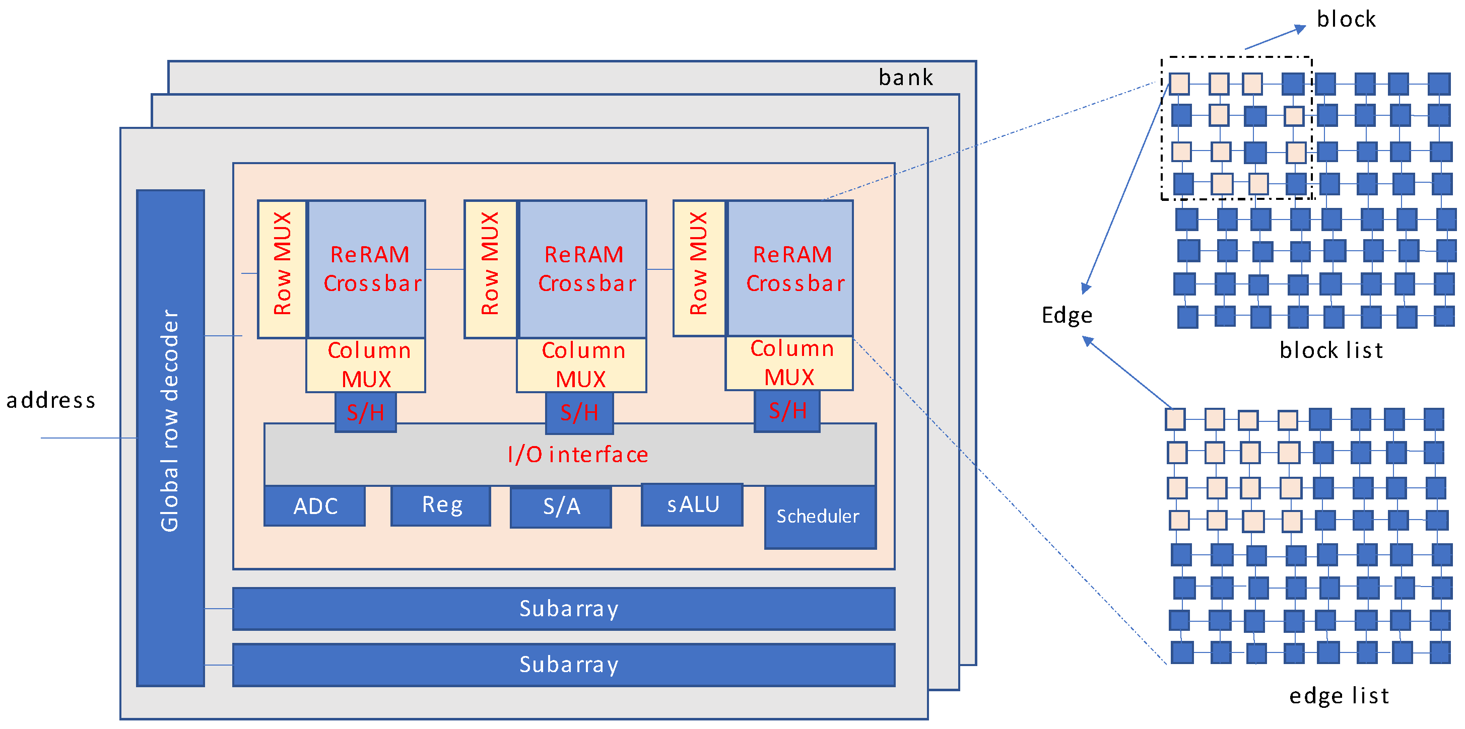
Figure 20 shows the overview of the GraphSAR topology. The edge data is both stored and computed in the ReRAM crossbars. The data is allocated in edge list format as well as block list, as demonstrated in Figure 19. Data from the reg (register) file is utilized by both crossbars and simple ALUs. Data loading and scheduling is taken care of by the scheduler. The architecture also includes sample and hold unit as well in order to convert analog data into digital by using an analog to digital converter. The authors of [23] proposed light weight clustering method in which only denser blocks are processed, while others are skipped. This method decreases blocks to be under procedure. Therefore, it significantly reduces the memory overhead.
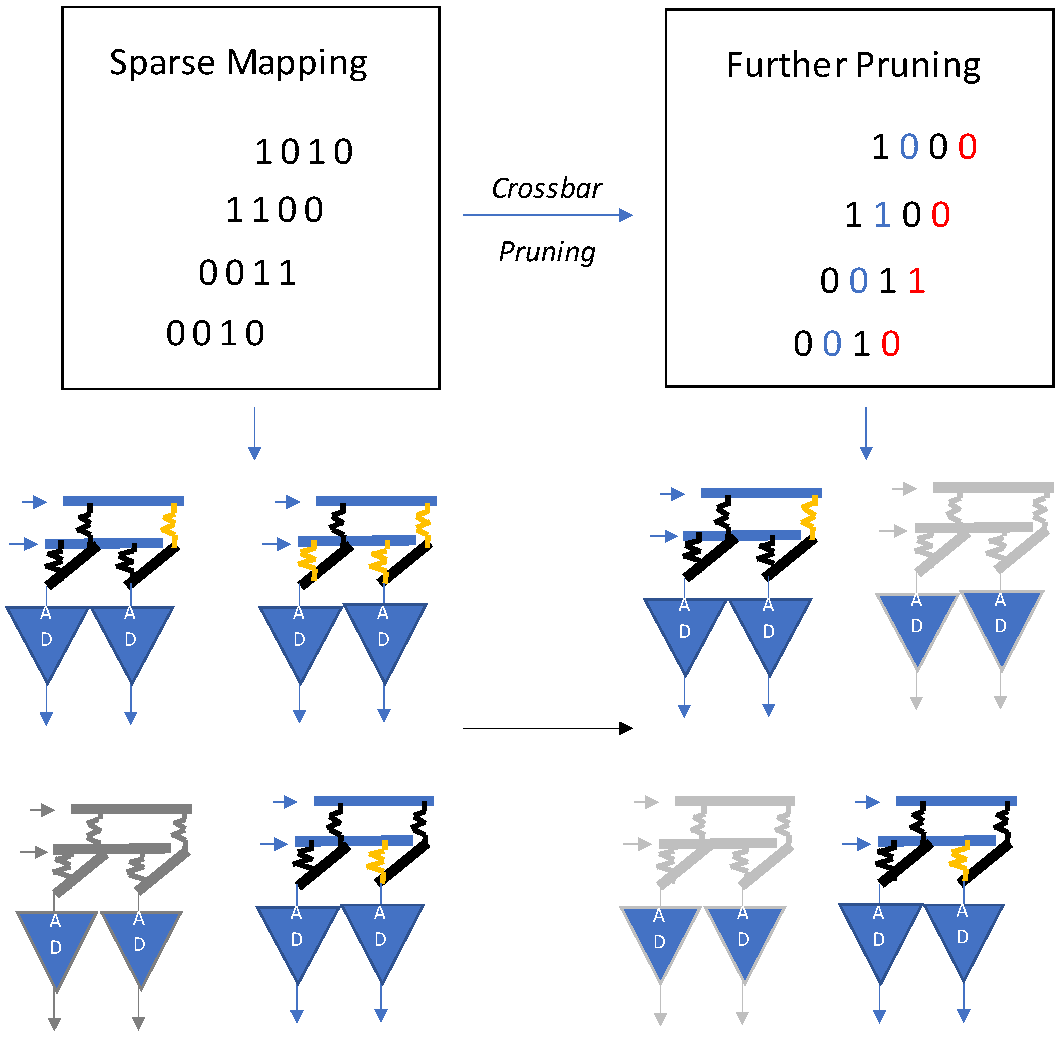
ReRAM-based NN accelerators have promising features but most of them lack the ability of efficient mapping for sparse neural networks. To overcome this limitation and improve crossbar utilization of ReRAM, a sparse neural network technique is proposed in [24] as illustrated in Figure 21. It is based on clustering, i.e., shuffling of columns in a weight matrix. The nonzero crossbars are also eliminated. The prime aim of this scheme is to use lesser crossbar arrays.
The mapping design is based on two prime observations. Firstly, in most neural networks, the weight matrix is massive, which is not possible to map onto a singular ReRAM crossbar block—it has to be divided into sub-blocks. Secondly, to show the pros and cons of the matrix, two crossbars are required. Therefore, the density goes to half the original size because 98 percent of the matrix values become zero. As per these findings, elimination of these zero elements can improve the crossbar utilization. The sparse neural network is further compressed by elimination of crossbars with low utilization. The authors of [24] also propose a crossbar-grained pruning algorithm as shown in Figure 22.
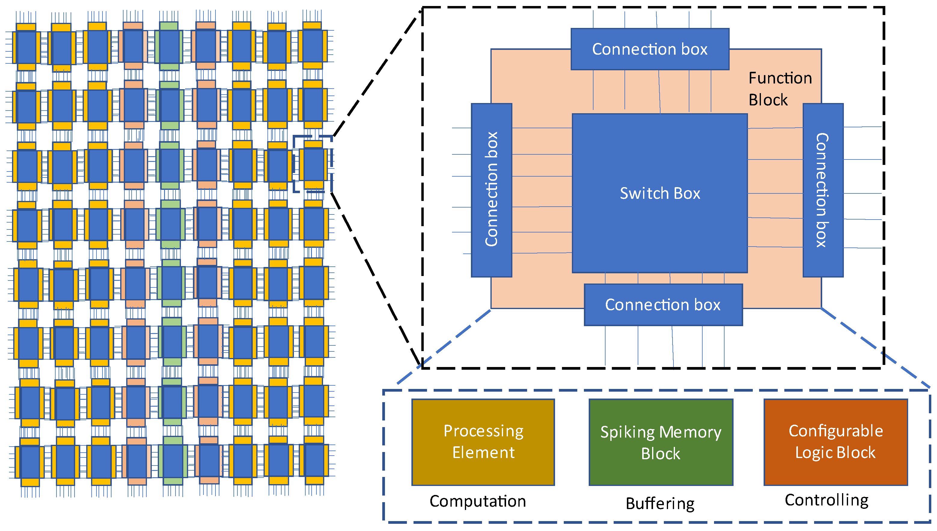
FPSA is an NN accelerator [25] with ability in memory processing based on the ReRAM technology. In previous works [21,22,23,24], the pros of high efficiency and density of ReRAM are not completely fully understood and applied because of the large demands of communication among PEs and the peripheral circuit overheads. Earlier approaches [21,22,23,24] apply a memory bus or a mesh-based NoC for communication purposes for PEs in ReRAM-based NN accelerators. In those works, memory buses and NoCs are unable to appease the large communication cost of the PEs. FPSA has been implemented to increase the production of ReRAM based on the NN accelerators improving their volume in current interconnections as well as the requirements of the ReRAM. A reconfigurable routing architecture has been proposed by the FPSA to provide a distinctively large among of communication capacity through the wiring resources. FPSA does not apply memory buses or NoCs among the PEs. With enabling various paths with a large communication bandwidth during an off-line reconfiguration phase by the FPSA, the communication demand among the PEs is satisfied. Since the configuration of the neural network models such as the DNN are static, applying a runtime flexibility is not meaningful, while previous researches [21,22,23,24] recycle physical channels to plan a path among the PEs and provide a runtime flexibility. Therefore, FPSA proposes a fixed-time datapath and determines a physical channel for every signal in advance. ReRAM-based connection boxes (CB) and switch boxes (SBs), proposed by [25] shown in Figure 23, connect PEs in order to minimize the area consumed and compensate for the high amount of fan in/outs of PEs. Authors in [25] mention that in compared with PRIME [22], the ability of the FPSA can improve the computational density by about 31×.
Every NN possesses two stages, training and testing. In the testing phases, the network’s weights have been established and data drifts via the layers in a forward path. Before using neural networks in any application, it is required to move into the training stage in which the weights are generated by the model. The data moves bidirectionally to update the weights. In [26], training and testing are aided in a ReRAM-based accelerator called Pipelayer. Interlayer parallelism is carried out with an effective pipeline system in which data constantly drifts in the accelerator at successive cycles. In addition to it, the pipelayer architecture utilizes a spike-based scheme for data input instead of voltage level. The overhead of ADC and DACs is removed in such a manner.
Pipelayer configuration immediately utilizes the ReRAM cells in order to carry out computations regardless of the processing units. Figure 24 shows the pipelayer architecture to process the training phase of a neural network. The main memory is spilt into two categories, morphable and memory subarrays. The memory subarrays can store data while the morphable subarrays can both store data and carry out computations. In Figure 24, the memory subarrays are represented by circles and rectangles represent morphable subarrays. The results of computations carried out at morphable subarrays are stored in memory subarrays.
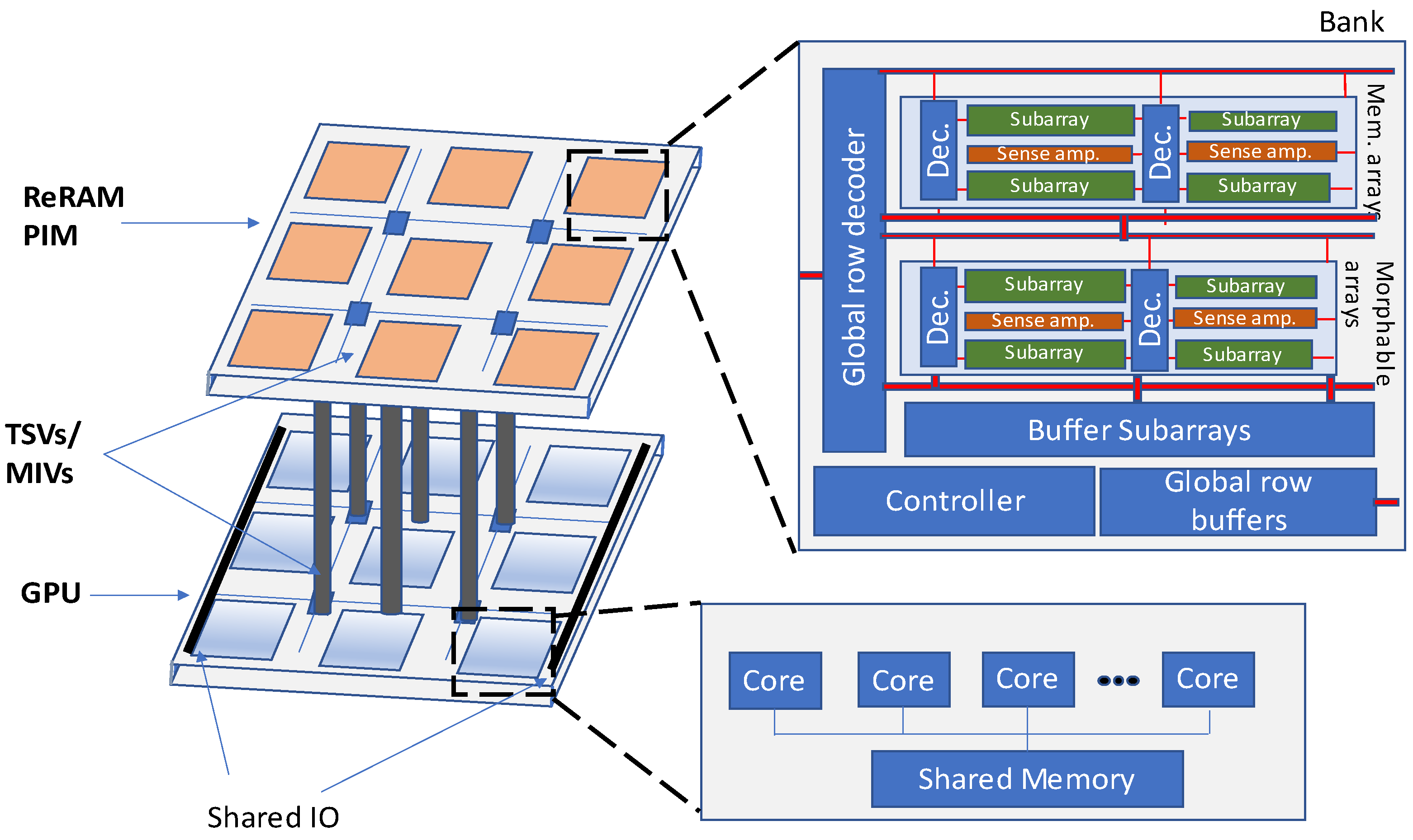
3D-ReG is another ReRAM-based heterogeneous manycore system that has been proposed for accelerating of the training phase of deep neural networks [27]. 3D integration and ReRAM are two technologies that have been applied for designing the 3D-ReG. A processing-in-memory (PIM) design based on the ReRAM technology has been introduced in [27] to accelerate the DNNs. The designed PIM possesses two distinct array types, memory and morphable arrays. Memory arrays are used as standard data storage whereas morphable arrays are enabled to jump between the data storage and computational data. A ReRAM layer has been stacked on the GPU layer in the 3D-ReG architecture as shown in Figure 25.
Another ReRAM-oriented deconvolution architecture (RED) design of neural accelerator has been proposed in [28]. The performance is analyzed for deconvolution execution for pre-existing PIMs. Extra operations are disregarded to improve the utilization.
Figure 26 illustrates the overall presented ReRAM deconvolution architecture (RED). A local input buffer is common for various processing elements to omit the inserted zeroes. The single functional (SFB) and multifunctional (MFB) registers in the input buffer allow the reuse of data with shift and buffer modes. When in shift mode, the buffers shift the data required for carrying out the computations. On the other hand, the buffer mode is used to load the data from memory or supply to the processing elements. Each processing element (PE) consists of an array of ReRAM crossbars and peripheral devices as decoders, multiplexers, and read circuits. For a computational result, the outputs from a PE cluster are selected via multiplexer and are added to compute the final result.
Firstly, a pixel-wise mapping scheme is carried out which maps the kernel weights to resistive RAM arrays at a very fine level. Parallel execution of various computation modes is facilitated through this technique. Secondly, in order to facilitate the reuse of input data, a zero-skipping data flow technique is also presented. In this mode, only the novel inputs are dispersed in various processing elements for extreme data reuse and concurrent execution.
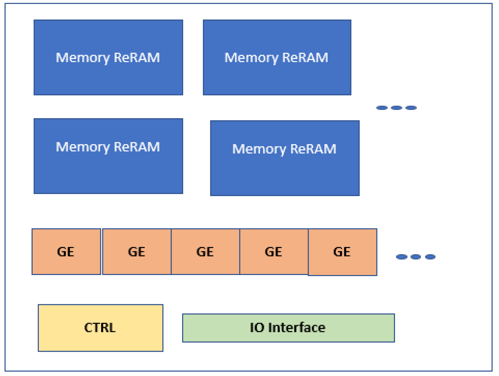
Another Re-RAM-based graph processing accelerator is presented in [29]. It is based on near-memory processing to facilitate lower energy and hardware overheads. As shown in Figure 27, each GraphR node consists of two main blocks, ReRAM memory blocks, and graph engines. Meanwhile, memory ReRAM stores the original graph data and graph engines carry out matrix-vector multiplications through numerous peripheral devices. It also includes a series of ReRAM memory crossbars. Additionally, sample and hold components, controllers, analogs to digital converters, drivers, shift and add units, and input/output registers are some parts of a graph engine.
This paper utilizes a streaming–application execution model that processes each subgraph in a streaming fashion. The execution is carried out in two alternatives: column major and row major. The processing of subgraphs with same destination vertices is carried out together in the column major, while in the row major, the processing of subgraphs with same source vertices is handled together. In this manner, the column major requires lesser output registers while the row major needs few input registers. GraphR carries out execution using column-major alternatives as it needs lesser output registers.
Summary and Discussion
This section assesses resistive ReRAM-formed memory architectures for DNN accelerators. The reviewed papers show that atomic layer computations in ReRAM promise effective pipelining. In some works, memristors are utilized to perform neural computations instead of DRAM. ReRAM-based memory architectures promise excessive benefits for graph processing with an ability to both store and compute data in crossbars. Some parts of research also defend an increase in capacity of DNN accelerators with an amalgam of processing-in-memory with ReRAM. Section 6 discusses features of processing-in-memory architectures in DNN accelerators.
5. Nonvolatile Memories (NVMs)
Despite the high degree of parallelism offered by GPUs, DNN workloads have massive memory footprints and work to further worsen the memory bottleneck of the system. As a solution in [20], nonvolatile memories (NVMs) such as STT-RAM [30] show more promise than conventional SRAM, but due to NVM technology’s absence from the commercial market, there is a need for a design space for further exploration of it. To this end, DeepNVM was developed to provide guidelines in order to analyze, distinguish, and optimize NVM-based caches for GPU architectures. It has the ability to assess the power, performance, as well as the area of NVMs in application in the last-level cache in the GPU.
NVSim, another modeling tool for NVM technologies, was incorporated into the DeepNVM framework to develop additional functionality. Since NVSim disregards the architecture-level analysis and applications’ specific memory behavior, it cannot perform cross-layer analysis on NVM technologies. Thus, NVSim is integrated with DeepNVM’s advanced architecture-level ISO capacity and area, as well as area analysis flow to enable the investigation of the design space of both the latest NVM caches as well as the SRAMS such as STT-RAMs.
This paper performs an evaluation in regards to the spin-transfer torque MRAM (STT-MRAM) in addition to the spin-orbit torque MRAM (SOT-MRAM) using the developed framework in a GPU-based DNN accelerator and makes the following notable findings when compared against the baseline performance of SRAM:
- STT-MRAM consumes 2.17× dynamic energy and SOT-MRAM uses 1.02× more dynamic energy
- STT-MRAM and SOT-MRAM have 6.6× and 8.5× lower leakage energy respectively.
- In general, STT-MRAM and SOT-MRAM possess an energy reduction of 5.6× and 7.7× respectively.
- Lastly, both STT-MRAM and SOT-MRAM supply a decrease in area of 2.4× and 3.0× respectively.
Summary and Discussion
This section reviews scope of nonvolatile memory-based DNN accelerators. Recent works reflect that deepNVM is one such structure, which analyzes performance parameters for NVMs used as last-level caches (LLCs) in GPGPU architectures.
6. Processing-in-Memory (PIM)
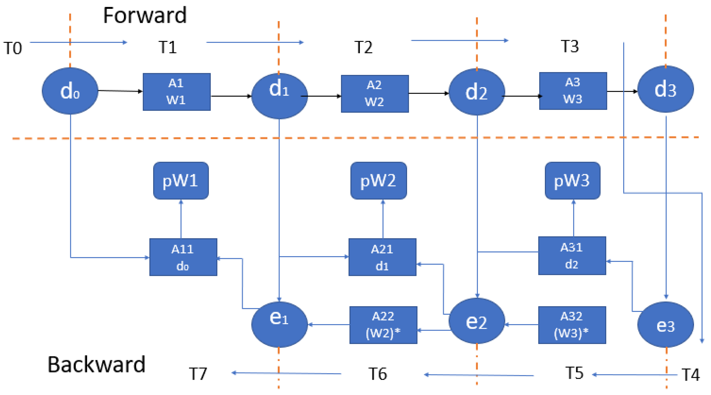
Unlike 3D memory and ReRAM-based memory architectures, processing-in-memory is another rich memory technology that has wide scope in design of efficient neural networks. Yet, PIM architectures have certain challenges that need to be addressed. Firstly, it is difficult to obtain computations of high precision with PIM. Also, PIM architectures face the limitation of nonscalability of analog/mixed circuits designs. These challenges are catered in FloatPIM architecture proposed in [13]. In the presented architecture, out of 32 tiles in PIM, every tile embraces a memory block with 256 crossbars with row and column drivers. The switches allow simultaneous flow of data between different blocks of memory. The operations of switches and row and column drivers are synchronized by a controller. Float PIM architecture incorporates digital data storage features which enables block-size scalability with need of lesser memory subblocks for computations. The memory blocks are arranged in such a manner that each of the blocks is connected to two of its adjacent neighboring blocks. This arrangement allows effective row-parallel communication in between the blocks. At first cycle of the clock (To), all the memory blocks work parallelly in computing mode. In the other two cycles, T1 and T2, the blocks operate in data transfer mode. In T1, the odd-numbered blocks send data to neighboring blocks, while in T2, data is transferred by even-numbered blocks. In this manner, the complete data transfer is carried out in only two consecutive cycles.
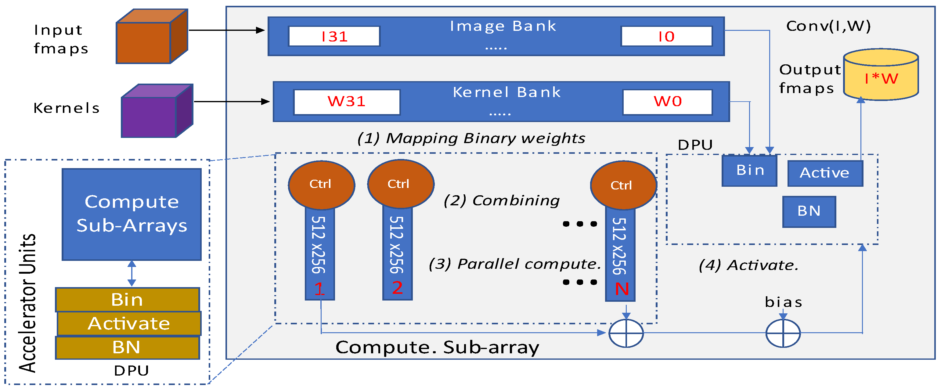
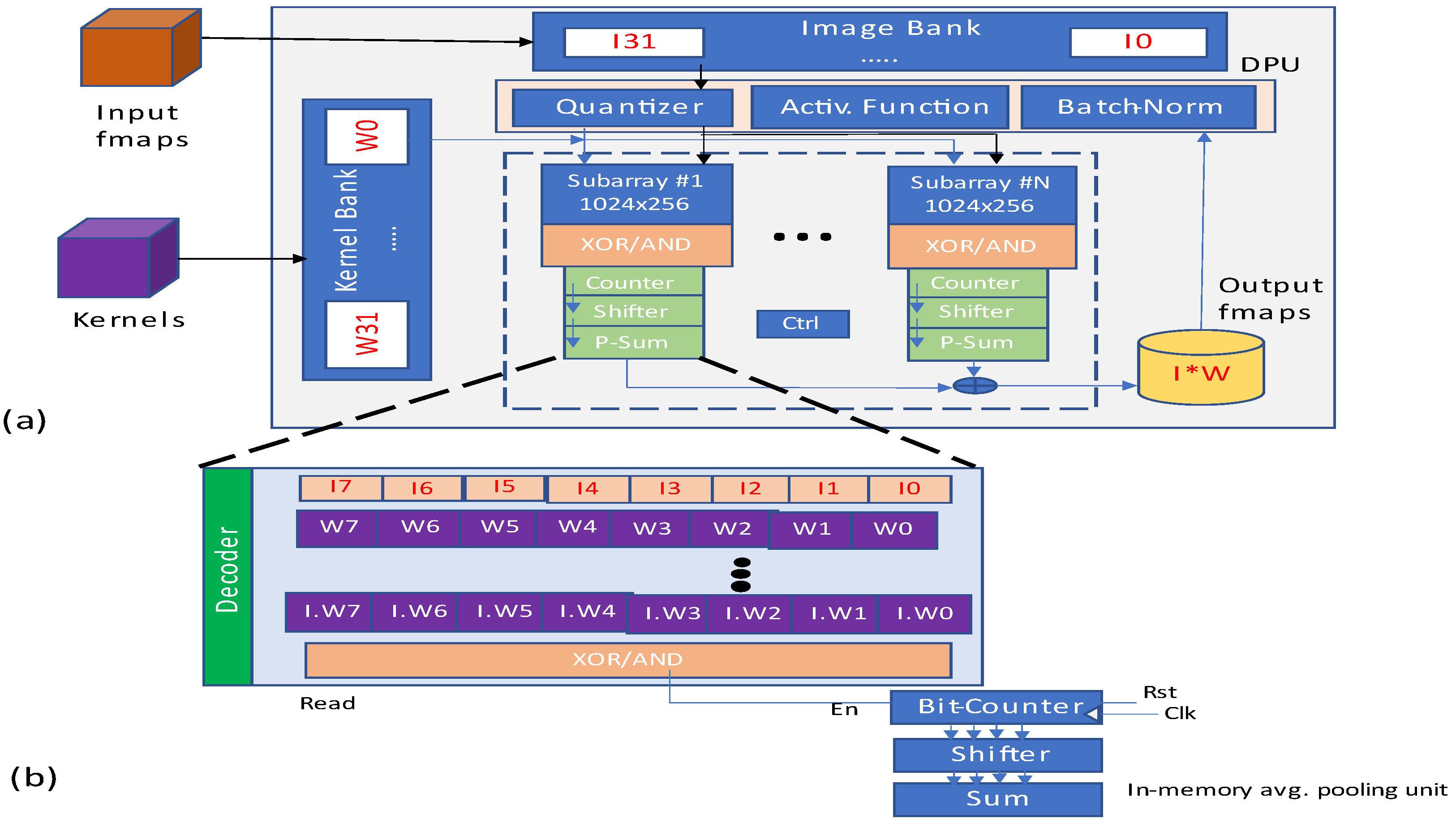
In [14], another PIM-based architecture is a proposal that focuses on an energy efficient design possessing high-performance binary weights in deep neural networks. A presented architecture, ParaPIM, aims at achieving parallel access of spin-orbit torque magnetic random access memory subarrays for efficient and high-speed BWNNs.
The structural block diagram of presented ParaPIM as depicted in Figure 28, broadly involves image and kernel banks, memory subarrays, and a digital processing unit. Before the mapping of kernels into memory subarrays, they are binarized by binary unit of DPU. The obtained results are further drawn to corresponding subarrays. The ParaPIM subarray structure is also depicted in Figure 28. It can be operated in double mode for both read/write memory operations and bit-line computations.
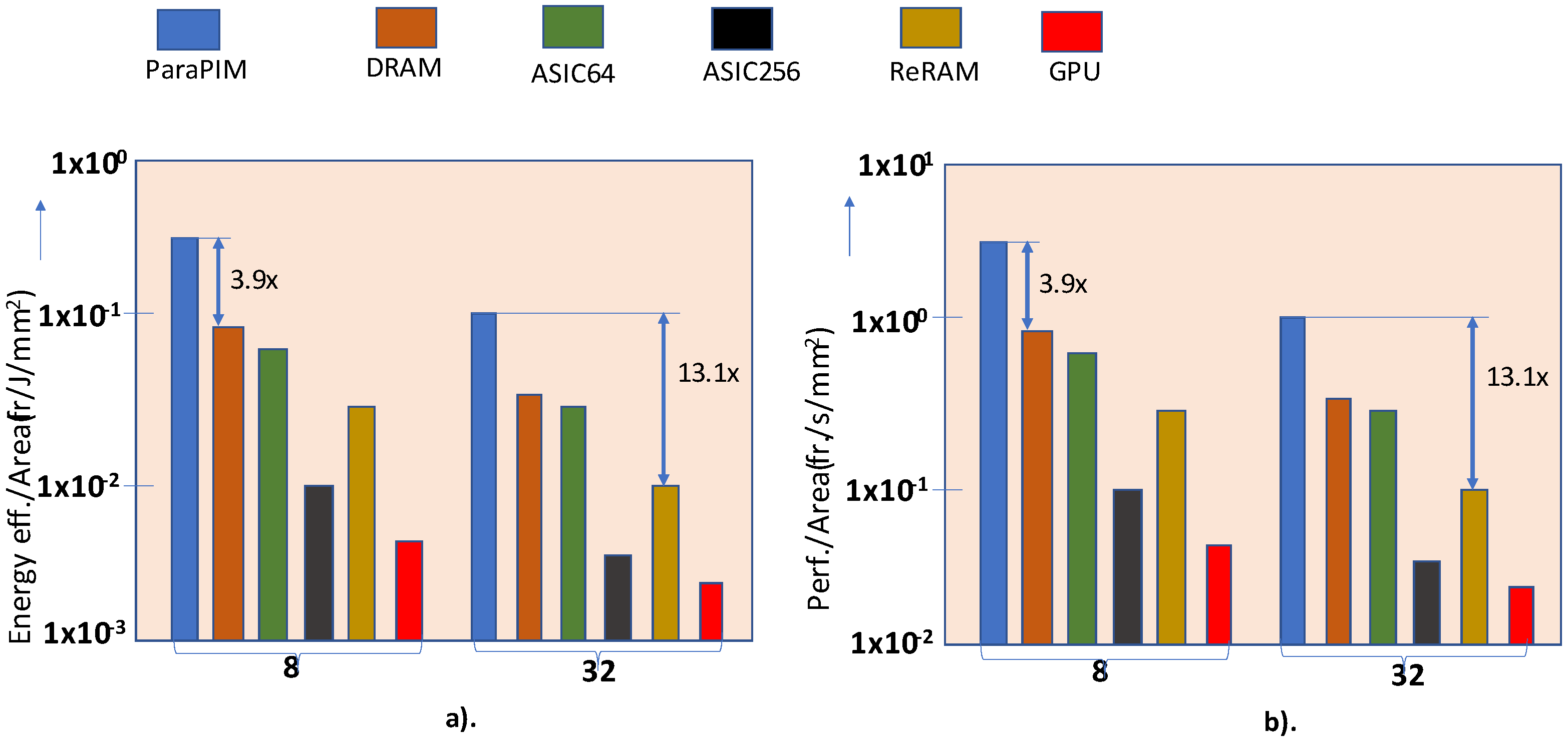
The comparison results of different memory architectures on the BWNN model are gathered in [14] for a common task considering batch sizes of 8 and 32 as shown in Figure 29. It is witnessed that ParaPIM is at least 3.9 times a more energy-efficient model than DRAM for batch size 8. Also, when considering a comparison with a ReRAM-based model with batch size 32, ParaPIM comes out as being 13 times more energy efficient. Likewise, the super-fast and in-situ operations place it ahead of other technologies in terms of performance as well.
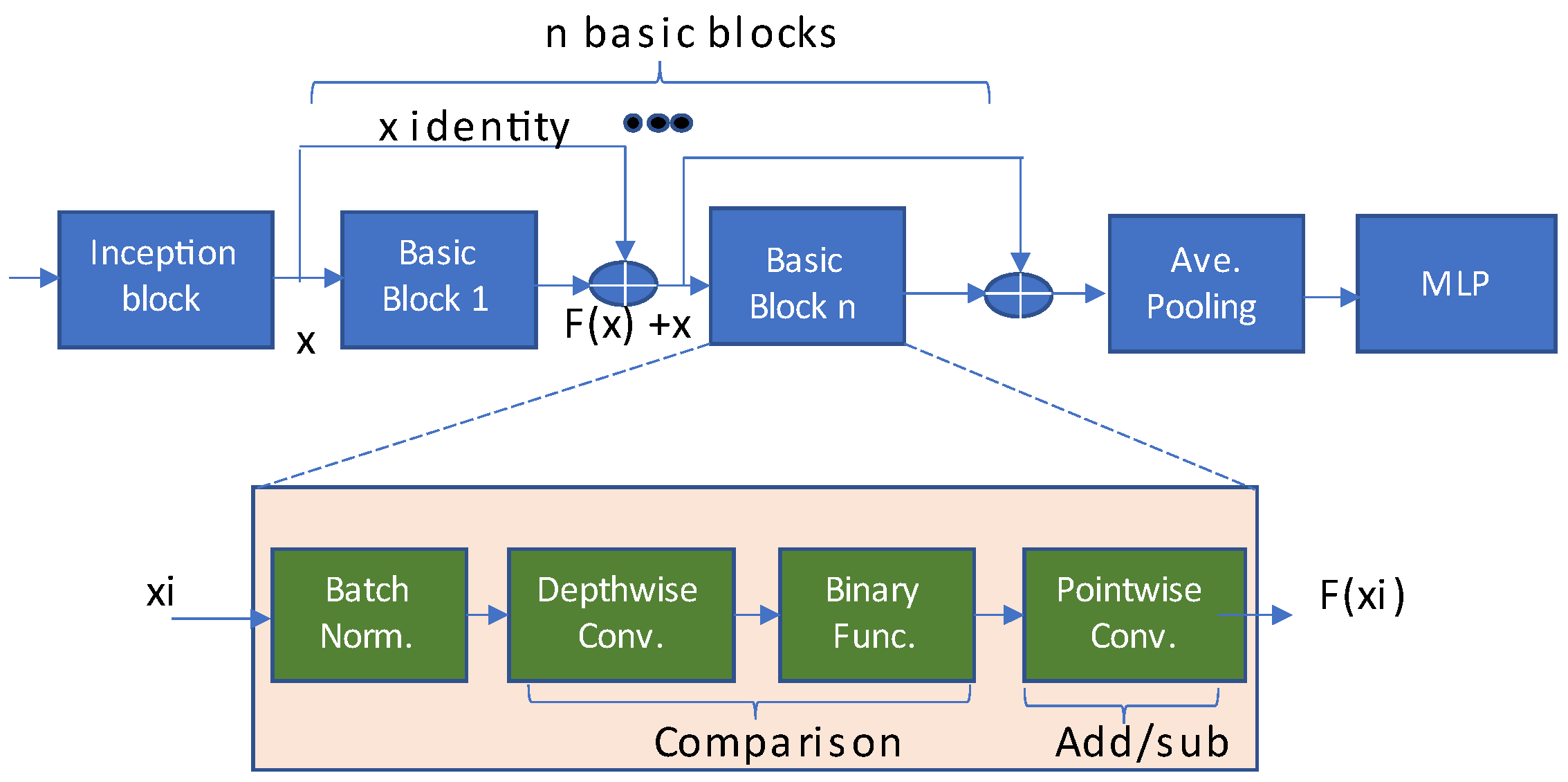
Paper [15] presents a comparator-based PIM memory architecture accelerator design for a fast and efficient comparator-based neural network. The presented architecture utilizes parallel SOT-MRAM-based memory subarrays as processing units. The pre-existing CNN algorithms are altered by substituting convolution layer multiplications with lesser complex additions and comparisons as depicted in Figure 30.
The basic block comprises a set of operating functions as batch normalization, depthwise and pointwise convolution. Figure 31 depicts the presented CMP-PIM architecture, and it comprises image and kernel banks, memory subarrays, and a digital processing unit. Before the mapping of kernels into memory subarrays, they are binarized by binary unit of DPU. The obtained results are further drawn to corresponding subarrays.
Liu et al. in [17] have proposed a processing-in-memory architecture derived from a runtime system considering a system gleaned from a runtime design.
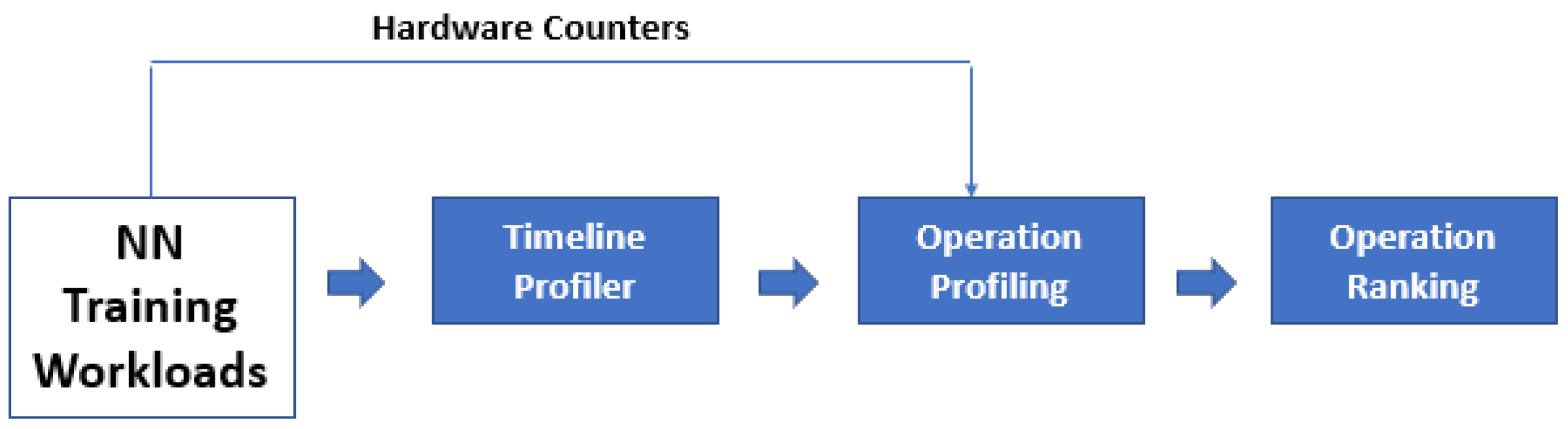
According to the authors’ observations in [17], the most time-consuming operations, which dominate in the training phases of the DNNs, are the most memory intensive. Based on their observations, simply executing pure multiplication and summation are inadequate for cumbersome memory exhaustive computations. Relu, MaxPool, ApplyAdam, Conv2DBackpropFilter, and Conv2DBackpropInputs are the best example functions in DNNs’ training phases, which are composed of operations and logic beyond the capacity of simple summation and product computations [16]. These comprehensive operations have the capability to exhaust on average 40% of the total implementation time of the DNNs based on the study in [17]. This observation shows a heterogeneous computation requirement in DNNs. Therefore, a heterogenous PIM design which intertwines microprocessor based/programmable cores and fixed function logic has been proposed in [17]. In the presented architecture, a runtime framework oversees time-based computations for CPU, fixed function PIM, and programmable PIM. The runtime framework includes two steps, profiling and scheduling.
In the profiling phase, the runtime framework for each clock cycle tracks every computation with a hardware counter accumulating the amount of main memory access-level cache misses and the execution time shown in Figure 32. The runtime framework makes a decision derived from the profiling results about determining the eligible functions, which can be outsourced to the CPUs and PIMs. In making the decision, the runtime framework organizes operations into two categories determined by the amount of main memory accesses and execution times. These categorical lists are in descending order and every computation in each list has one index. The runtime framework generates a global index by the summation of the two respective indexes. A global list is generated by organizing all operations evolved from their respective global indexes. Finally, from this global list the top operations are chosen to unburden the PIMs via the runtime framework. In the scheduling phase, the runtime framework schedules the given candidate operations to offload to CPU, fixed function PIMs, and programmable PIM based on a set of principles mentioned in the paper.
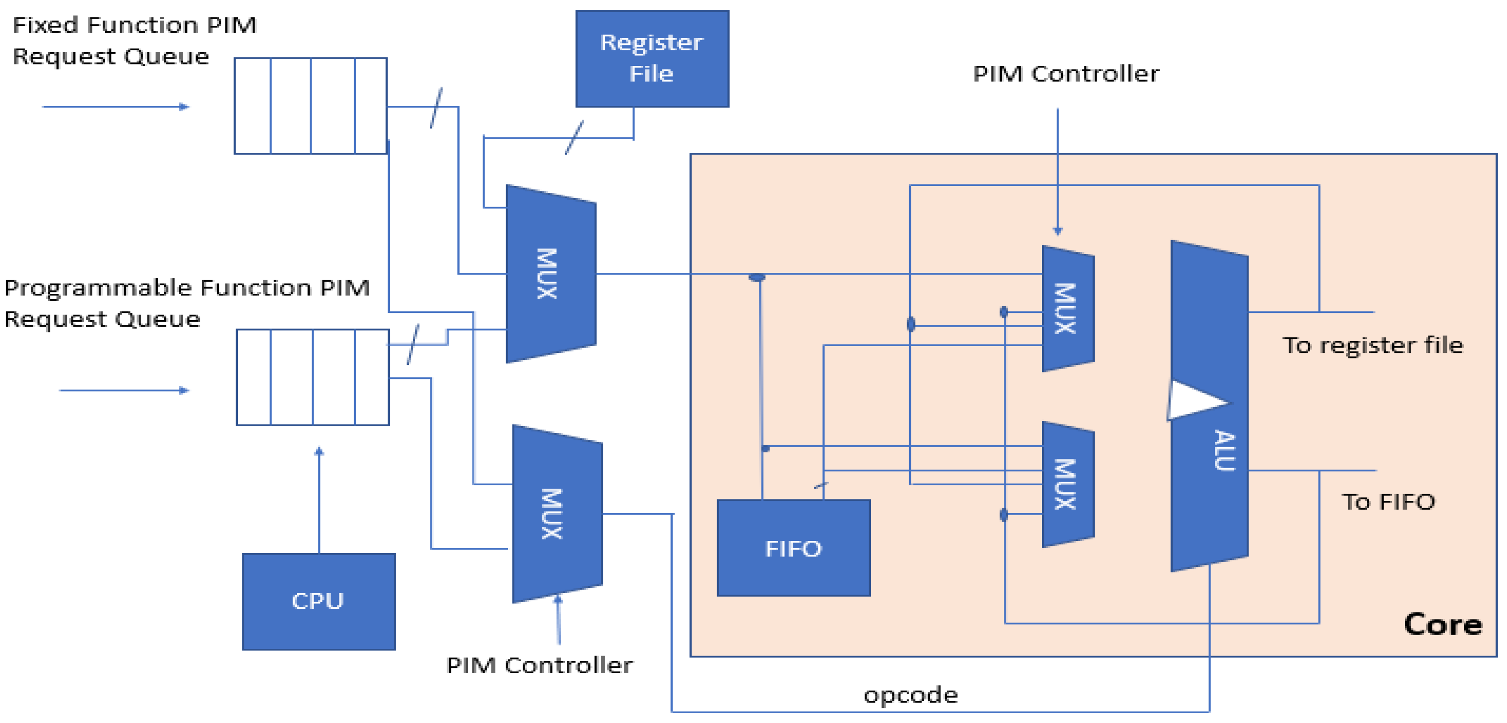
A heterogeneous PIM architecture is proposed in [17]. This particular software/hardware scheme encourages fast data communication between memory and processors (Figure 33). The presented design broadly has three key mechanisms. Firstly, fixed function logic blocks and programmable hubs are stacked in a 3D network to form heterogeneous architecture. Secondly, the programming challenges are catered by the OpenCL model. Then, a runtime system is presented to maximize hardware utilization and operation parallelism.
The runtime system proposed in [17] includes two main features. Firstly, it includes a pipeline scheme to simultaneously run multiple neural network operations. Secondly, it also includes a recursive method to call the fixed function PIMs. Hardware utilization is considerably improved through these topographies.
To achieve a bit precision reconfigurable digital in memory computing macro, smaller components called bitcells are used in [18]. A macro consists of a 128 by 128 bitcell array. Each bitcell is comprised of three parts:
- (1)
- 6T SRAM cell: stores binary values for weight.
- (2)
- Bitwise multiplier replicated by an XNOR gate.
- (3)
- Full adder: carries out bitwise addition.
An implementation of parallel configured neurons can be represented by bitcell arrays. Furthermore, it was found that bitcell arrays have the capability to be reconstructed into parallel row neurons. A neuron consists of 128 column-shaped multiply and accumulate units (column MACs) arranged in a row. A bitcell array, dependent on precision settings, can be manipulated to adapt to various N bit column MACS up to 16-bit precision. An advantage this architecture holds over conventional processing methods is the number of components required to achieve the desired bit precision. In conventional arithmetic logic, the multiplier size grows quadratically as bit precision increases. However, this architecture’s multiplier size grows in proportion to the bit precision. On a 65 nm test chip, the energy efficiency is reported as 117.3–2.06 TOPS/W for 1- to 16-bit precision respectively.
Summary and Discussion
This segment of the article examines processing-in-memory (PIM) which is another promising memory architecture used in DNN accelerators. Though PIM permits faster communication between the processor and memory, high-precision achievement has been a challenge. Recent works show that floatPIM enables block size scalability with its digital storage capabilities. A comparator-based PIM architecture offers rich scope for fast and efficient neural networks. Another work illustrates that parallel access of memory subarrays in PIM promises an upsurge in energy efficiency. A combination of fixed-function logic and programmable cores in heterogeneous processing-in-memory also supports fast data communication.
7. Near-Memory Processing
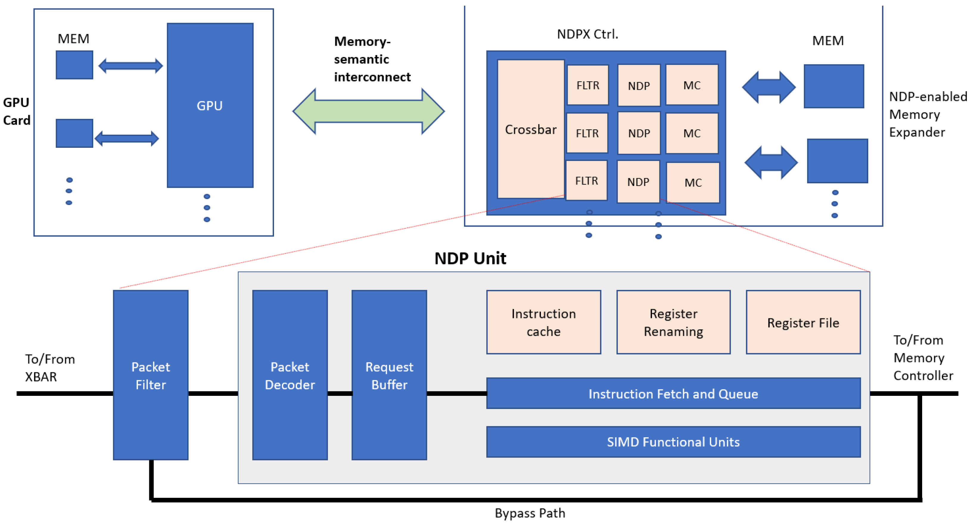
In an attempt to reduce the memory wall in the training processes of neural networks, in [19] the near-data processing enabled eXpander (NDPX) is developed as a nonintrusive method to handle memory-bound operations to increase the allocated GPU memory storage. Since NDPX minimally modifies the GPU architecture, it can be easily implemented with GPUs from various vendors.
Memory-bound operations can consume a significant portion of memory capacity and considerably hinder the training process by lengthening train time and limiting training throughput. Batch normalization is one such process which optimizes all the activations in every channel for the same batch and normalizes them. In addition to this, the average in addition to the variance is also realized in the batch normalization training process. This stabilizes the distributions of activations in the batch. The pooling layer is another memory-bound operation that downsamples 4 × 4 activations in input tensors to a 2 × 2 output. Additionally, to update the model parameters, element-wise operations are commonplace in order to integrate the respective layers’ output feature maps. These operations are examples of processes the NDPX will accelerate, so as to free memory in the GPU to speed up training. The NDPX has a direct connection through a high-speed memory semantic connection to the GPU. This consists of an NDPX controller as well as DRAM devices. Figure 34 illustrates the NDPX architecture and its interaction with the GPU.
Each memory controller has a dedicated NDP unit and packet filter per memory channel, and is capable of simultaneously executing multiple requests. When a response packet via the memory controller or a request by the GPU containing physical address corresponds to a filter entry, an NDP kernel function is executed. This is done to replace a GPU kernel in order to offload the memory-bound operations to the NDPX. As a result, the GPU possess additional free memory to handle other operations to continue training. The NDPX architecture has been shown to speed up training for VGG-16 by 51%.
8. Off-Chip Memory Architectures in DNN Accelerators
We have reviewed different on-chip memory architectures in DNN accelerators in the previous sections. Three off-chip memory organizations are reviewed in this section.
The access to off-chip memory imposes a big limitation on the energy efficiency of CNN (convolution neural networks) accelerators. One technique to decrease DRAM access is data reuse, but specific data reuse can minimize memory access for only the respective data type. Therefore, sticking to one data type does not solve the issue for the entire network and will cost for reuse of other data types. The authors of [32] offer a promising layer partitioning and scheduling scheme, called Smart Shuttle. An analytical framework is presented to measure DRAM access volume and find suitable sectionalization and scheduling arrangement for every layer.
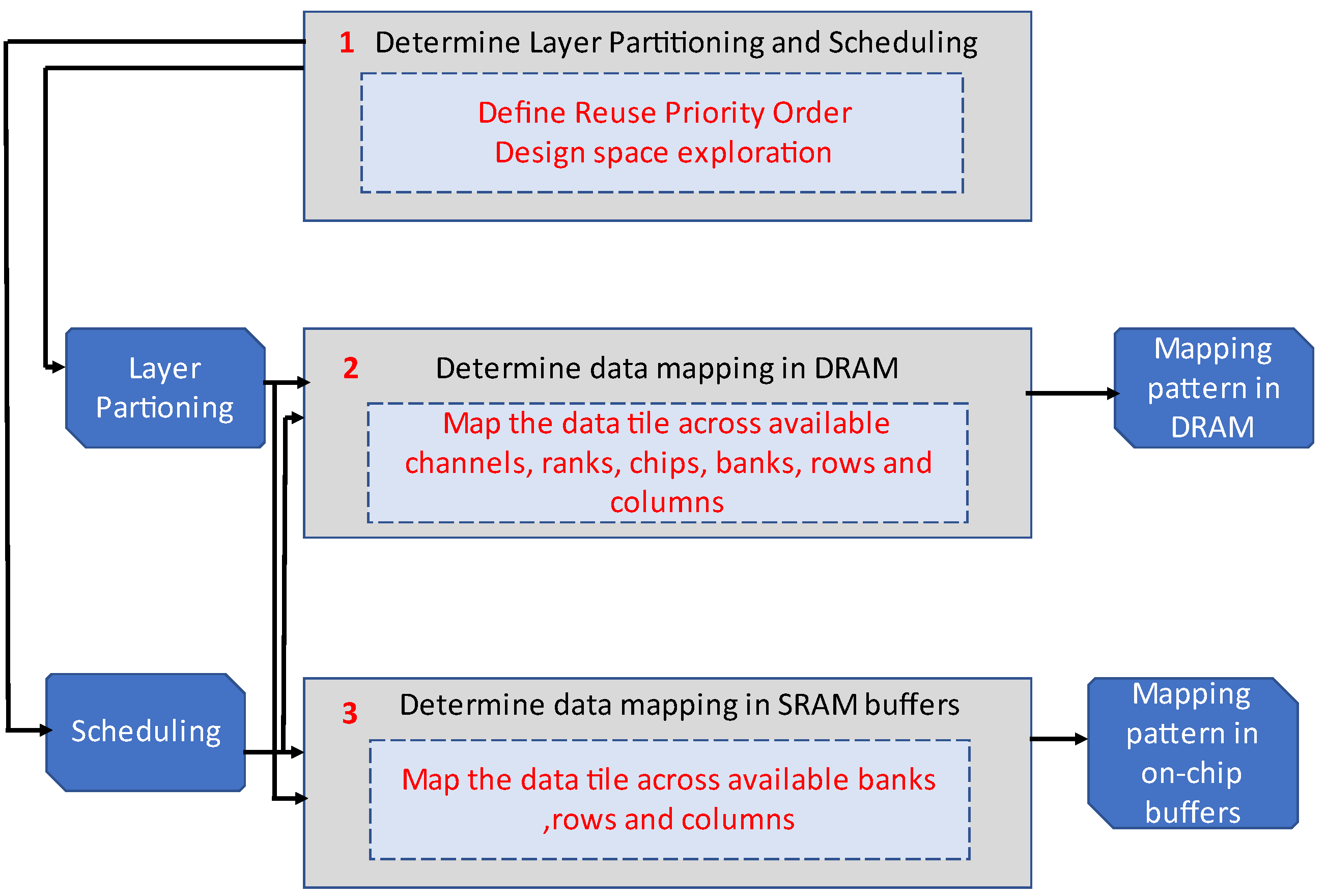
Another methodology named ROMANet, for promising DRAM access energy savings is proposed in [33]. It empowers effective reuse off-chip memory access management and data arrangement. DRAM energy access shows dependency on number of DRAM accesses, row buffer misses and conflicts. The authors of [33] offer an analytical model to optimize these parameters. The data mapping in off-chip DRAM improves throughput and reduces DRAM access energy. Along with it, the data mapping in on-chip SRAM buffers supports bank-level parallelism. Figure 35 shows the flow of operation of ROMANet methodology.
Unlike conventional DNNs, capsule networks (CapsNets) are capable candidates that offer multidimensional capsules rather than one-dimensional neurons. However, the memory requirements are likewise high, triggering necessity of energy efficient on-chip memories. The authors of [34] analyze design challenges for on-chip memories deployed in CapsNets accelerators. DESCNet, a multibanked memory architecture, is proposed, which is based on dataflow mapping and respective memory access patterns of various steps of CapsNet inference.
9. Summary of the Paper
The approaches we discussed in this paper are summarized in Table 1. In addition, Table 2, which is a ranking table for reviewed architectures in this work, indicates certain factorials such as throughput, power consumption, footprint, technology node, and energy efficiency. Throughput can be considered as a parameter to show accelerated computation, and power consumption, footprint, and energy efficiency can be good parameters to show the cost and simplicity of each method. In addition, a column related to the specific application for each method has been considered for this table.
10. Conclusions
As the number of applications for NNs and DNNs are increasing, the demand for hardware accelerators is also growing. To conquer the memory wall challenge, memory system configuration is attracting more focus these days. In order to achieve goals of flexible DNN execution as well as overall performance, different memory architectures have been presented and considered in the DNN’s design in different research papers. This study assessed that designing of energy-efficient memory architectures causes an improvement in power consumption and performance of DNN accelerators significantly.
Emerging technologies, namely in memory processing, near-memory processing, and nonvolatile memories have the ability to diminish the drawbacks of traditional memory systems. Unlike the broad pre-existing surveys on DNN accelerators, in this survey paper we reviewed the most common memory architectures proposed so far for enhanced power and performance.
In addition, we showed that DNNs have the capability to implement advanced technologies for better efficiency. This encompasses using 3D stacked and nonvolatile memories. Furthermore, these modern technologies can also allow the computation to shift closer to the source. This is done by setting the computation close to or within the memories and sensors themselves.
In conclusion, due to the proliferation of DNNs in different routine applications, DNNs are constantly growing in the areas of research and development. As such, the future holds many avenues of improvement and applications for various levels of hardware design.
Funding
NSERC funding.
Data Availability Statement
Not Applicable.
Conflicts of Interest
The authors declare no conflict of interest.
References
- Sze, V.; Chen, Y.H.; Yang, T.J.; Emer, J.S. Efficient processing of deep neural networks: A Tutorial and Survey. arXiv 2017, arXiv:1703.09039. [Google Scholar] [CrossRef] [Green Version]
- Raoux, S.; Xiong, F.; Wuttig, M.; Pop, E. Phase change materials and phase change memory. MRS Bull. 2014, 39, 703–710. [Google Scholar] [CrossRef] [Green Version]
- Asad, A.; Ozturk, O.; Fathy, M.; Jahed-Motlagh, M.R. Optimization-based power and thermal management for dark silicon aware 3D chip multiprocessors using heterogeneous cache hierarchy. Microprocess. Microsyst. 2017, 51, 76–98. [Google Scholar] [CrossRef]
- Kim, D.; Kung, J.; Chai, S.; Yalamanchili, S.; Mukhopadhyay, S. Neurocube: A programmable digital neuromorphic architecture with high-density 3D memory. ACM SIGARCH Comput. Archit. News 2016, 44, 380–392. [Google Scholar] [CrossRef]
- Gao, M.; Pu, J.; Yang, X.; Horowitz, M.; Kozyrakis, C. TETRIS: Scalable and Efficient Neural Network Acceleration with 3D Memory. In Proceedings of the Twenty-Second International Conference on Architectural Support for Programming Languages and Operating Systems, Xi’an, China, 8–12 April 2017; pp. 751–764. [Google Scholar]
- Joardar, B.K.; Kim, R.G.; Doppa, J.R.; Pande, P.P.; Marculescu, D.; Marculescu, R. Learning-based application-agnostic 3D NoC design for heterogeneous manycore systems. IEEE Trans. Comput. 2018, 68, 852–866. [Google Scholar] [CrossRef] [Green Version]
- Firuzan, A.; Modarressi, M.; Daneshtalab, M.; Reshadi, M. Reconfigurable network-on-chip for 3D neural network accelerators. In Proceedings of the 2018 Twelfth IEEE/ACM International Symposium on Networks-on-Chip (NOCS), Torino, Italy, 4–5 October 2018; pp. 1–8. [Google Scholar]
- Mohsen, I.; Samragh, M.; Gupta, S.; Koushanfar, F.; Rosing, T. RAPIDNN: In-memory Deep Neural Network Acceleration Framework. arXiv 2018, arXiv:1806.0579. [Google Scholar]
- Kim, J.S.; Yang, J.S. DRIS-3: Deep neural network reliability improvement scheme in 3D die-stacked memory based on fault analysis. In Proceedings of the 2019 56th ACM/IEEE Design Automation Conference (DAC), New York, NY, USA, 2–6 June 2019; pp. 1–6. [Google Scholar]
- Mittal, S. A survey on modeling and improving reliability of DNN algorithms and accelerators. J. Syst. Archit. 2020, 104, 101689. [Google Scholar] [CrossRef]
- Kim, D.; Na, T.; Yalamanchili, S.; Mukhopadhyay, S. DeepTrain: A programmable embedded platform for training deep neural networks. IEEE Trans. Comput. Aided Des. Integr. Circuits Syst. 2018, 37, 2360–2370. [Google Scholar] [CrossRef]
- Ueyoshi, K.; Ando, K.; Hirose, K.; Takamaeda-Yamazaki, S.; Hamada, M.; Kuroda, T.; Motomura, M. QUEST: Multi-Purpose Log-Quantized DNN Inference Engine Stacked on 96-MB 3-D SRAM Using Inductive Coupling Technology in 40-nm CMOS. IEEE J. Solid-State Circuits 2019, 54, 186–196. [Google Scholar] [CrossRef]
- Imani, M.; Gupta, S.; Kim, Y.; Rosing, T. FloatPIM: In-Memory Acceleration of Deep Neural Network Training with High Precision. In Proceedings of the 2019 ACM/IEEE 46th Annual International Symposium on Computer Architecture (ISCA), Phoenix, AZ, USA, 22–26 June 2019; pp. 802–815. [Google Scholar]
- Angizi, S.; He, Z.; Fan, D. ParaPIM: A Parallel Processing-in-Memory Accelerator for Binary Weight Deep Neural Networks. In Proceedings of the 24th Asia and South Pacific Design Automation Conference, Tokyo, Japan, 23 January 2019; pp. 127–132. [Google Scholar]
- Angizi, S.; He, Z.; Fan, D.; Rakin, A.S. CMP-PIM: An Energy Efficient Comparator-based Processing-in-Memory Neural Network Accelerator. In Proceedings of the 55th Annual Design Automation Conference, San Francisco, CA, USA, 24–29 June 2018; pp. 1–6. [Google Scholar]
- Li, T.; Zhong, J.; Ji, L.; Wu, W.; Zhang, C. Ease.ml: Towards multi-tenant resource sharing for machine learning workloads. In Proceedings of the 44th International Conference on Very Large Data Bases Endowment, Rio de Janeiro, Brazil, 27–31 August 2018; pp. 607–620. [Google Scholar]
- Liu, J.; Zhao, H.; Ogleari, M.A.; Li, D.; Zhao, J. Processing-in-memory for energy-efficient neural network training: A heterogeneous approach. In Proceedings of the 2018 51st Annual IEEE/ACM International Symposium on Microarchitecture (MICRO), Fukuoka, Japan, 20–24 October 2018; pp. 655–668. [Google Scholar]
- Kim, H.; Qian, C.; Yoo, T.; Kim, T.T.; Kim, B. A Bit-Precision Reconfigurable Digital In-Memory Computing Macro for Energy-Efficient Processing of Artificial Neural Networks. In Proceedings of the 2019 International SoC Design Conference (ISOCC), Jeju Island, Korea, 6 October 2019; pp. 166–167. [Google Scholar]
- Ham, H.; Cho, H.; Kim, M.; Park, J.; Hong, J.; Sung, H.; Park, E.; Lim, E.; Kim, G. Near-Data Processing in Memory Expander for DNN Acceleration on GPUs. IEEE Comput. Archit. Lett. 2021, 20, 171–174. [Google Scholar] [CrossRef]
- Inci, A.F.; Isgenc, M.M.; Marculescu, D. DeepNVM: A framework for modeling and analysis of non-volatile memory technologies for deep learning applications. In Proceedings of the IEEE 2020 Design, Automation & Test in Europe Conference & Exhibition (DATE), Grenoble, France, 9–13 March 2020; pp. 1295–1298. [Google Scholar]
- Qiao, X.; Cao, X.; Yang, H.; Song, L.; Li, H. AtomLayer: A Universal ReRAM-based CNN Accelerator with Atomic Layer Computation. In Proceedings of the 55th Annual Design Automation Conference, San Francisco, CA, USA, 24–29 June 2018; pp. 1–6. [Google Scholar]
- Chi, P.; Shuangchen, L.; Xu, C.; Zhang, T.; Zhao, J.; Liu, Y.; Wang, Y.; Xie, Y. Prime: A novel processing-in-memory architecture for neural network computation in reram-based main memory. ACM SIGARCH Comput. Archit. News 2016, 44, 27–39. [Google Scholar] [CrossRef]
- Dai, G.; Huang, T.; Wang, Y.; Yang, H.; Wawrzynek, J. Graphsar: A sparsity-aware processing-in-memory architecture for large-scale graph processing on rerams. In Proceedings of the 24th Asia and South Pacific Design Automation Conference, Tokyo, Japan, 23 January 2019; pp. 120–126. [Google Scholar]
- Lin, J.; Zhu, Z.; Wang, Y.; Xie, Y. Learning the sparsity for ReRAM: Mapping and pruning sparse neural network for ReRAM based accelerator. In Proceedings of the 24th Asia and South Pacific Design Automation Conference, Tokyo, Japan, 23 January 2019; pp. 639–644. [Google Scholar]
- Ji, Y.; Zhang, Y.; Xie, X.; Li, S.; Wang, P.; Hu, X.; Zhang, Y.; Xie, Y. Fpsa: A full system stack solution for reconfigurable reram-based nn accelerator architecture. In Proceedings of the Twenty-Fourth International Conference on Architectural Support for Programming Languages and Operating Systems, Providence, RI, USA, 13–17 April 2019; pp. 733–747. [Google Scholar]
- Song, L.; Qian, X.; Li, H.; Chen, Y. Pipelayer: A Pipelined ReRAM-Based Accelerator for Deep Learning. In Proceedings of the IEEE International Symposium on High Performance Computer Architecture, Austin, TX, USA, 4–8 February 2017; pp. 541–552. [Google Scholar]
- Li, B.; Doppa, J.R.; Pande, P.P.; Chakrabarty, K.; Qiu, J.; Li, H. 3D-ReG: A 3D ReRAM-based heterogeneous architecture for training deep neural networks. ACM J. Emerg. Technol. Comput. Syst. 2020, 16, 1–24. [Google Scholar] [CrossRef] [Green Version]
- Li, Z.; Li, B.; Fan, Z.; Li, H. RED: A ReRAM based Efficient Accelerator for Deconvolutional Computation. IEEE Trans. Comput. Aided Des. Integr. Circuits Syst. 2020, 14, 4736–4747. [Google Scholar] [CrossRef]
- Song, L.; Zhou, Y.; Qian, X.; Li, H.; Chen, Y. GraphR: Accelerating Graph Processing Using ReRAM. In Proceedings of the IEEE International Symposium on High Performance Computer Architecture, Vienna, Austria, 24–28 February 2018; pp. 531–543. [Google Scholar]
- Akinaga, H.; Shima, H. Resistive Random Access Memory (ReRAM) based on metal oxides. Proc. IEEE 2010, 98, 2237–2251. [Google Scholar] [CrossRef]
- Li, H.; Gao, B.; Chen, Z.; Zhao, Y.; Huang, P.; Ye, H.; Liu, L.; Liu, X.; Kang, J. A learnable parallel processing architecture towards unity of memory and computing. Sci. Rep. 2015, 5, 13330. [Google Scholar] [CrossRef] [PubMed] [Green Version]
- Li, J.; Yan, G.; Lu, W.; Jiang, S.; Gong, S.; Wu, J.; Li, X. SmartShuttle: Optimization off-chip memory accesses for deep learning accelerators. In Proceedings of the 2018 Design, Automation & Test in Europe Conference & Exhibition (DATE), Dresden, Germany, 19–23 March 2018; pp. 343–348. [Google Scholar]
- Putra, R.V.; Hanif, M.A.; Shafique, M. ROMANet: Fine-Grained Reuse-Driven Off-Chip Memory Access Management and Data Organization for Deep Neural Network Accelerators. IEEE Trans. Very Large-Scale Integr. Syst. 2021, 29, 702–715. [Google Scholar] [CrossRef]
- Marchisio, A.; Mrazek, V.; Hanif, M.A.; Shafique, M. DESCNet: Developing Efficient Scratchpad Memories for Capsule Network Hardware. IEEE Trans. Comput. Aided Des. Integr. Circuits Syst. 2021, 40, 1768–1781. [Google Scholar] [CrossRef]
Figure 1.
Classification of the memory architectures discussed in this survey.

Figure 2.
PRISMA flow chart followed for paper selection.

Figure 3.
Neurocube accelerator with detailed PE architecture. TSV: through silicon via [4].
Figure 3.
Neurocube accelerator with detailed PE architecture. TSV: through silicon via [4].

Figure 4.
Proposed programming and execution of a NN in Neurocube [4].
Figure 4.
Proposed programming and execution of a NN in Neurocube [4].

Figure 5.
The PE array sizes running VGGNET on Eyeriss under optimal scheduling for power consumption.
Figure 5.
The PE array sizes running VGGNET on Eyeriss under optimal scheduling for power consumption.

Figure 6.
Architecture of TETRIS [5].
Figure 6.
Architecture of TETRIS [5].

Figure 7.
Placement of LLC banks (yellow), GPUs (red), and CPUs (green) as a result of the proposed MOO method [6].
Figure 7.
Placement of LLC banks (yellow), GPUs (red), and CPUs (green) as a result of the proposed MOO method [6].

Figure 8.
The proposed ML-based MOO method [6].
Figure 8.
The proposed ML-based MOO method [6].

Figure 9.
Arrangement of a reconfigurable NoC [7].
Figure 9.
Arrangement of a reconfigurable NoC [7].

Figure 10.
The composition of a vault [7].
Figure 10.
The composition of a vault [7].

Figure 11.
Outline of RAPIDNN architecture [8].
Figure 11.
Outline of RAPIDNN architecture [8].

Figure 12.
Interpretation of computation of a neuron to sequence of operations in RAPIDNN network [8].
Figure 12.
Interpretation of computation of a neuron to sequence of operations in RAPIDNN network [8].

Figure 13.
SER of different layers in a 3D DRAM integration [10].
Figure 13.
SER of different layers in a 3D DRAM integration [10].

Figure 14.
Overview of Deeptrain architecture [11].
Figure 14.
Overview of Deeptrain architecture [11].

Figure 15.
Design structure of QUEST architecture proposed in [12].
Figure 15.
Design structure of QUEST architecture proposed in [12].

Figure 16.
Atomic-layer architecture for ReRAM-based DNN accelerator design. PE: processing element; GOB: global output buffer [21].
Figure 16.
Atomic-layer architecture for ReRAM-based DNN accelerator design. PE: processing element; GOB: global output buffer [21].

Figure 17.
The row-disjoint filter mapping technique proposed in [21].
Figure 17.
The row-disjoint filter mapping technique proposed in [21].

Figure 18.
An overview of the (a) traditional shared memory, (b) 3D PIM, and (c) PRIME [21].
Figure 18.
An overview of the (a) traditional shared memory, (b) 3D PIM, and (c) PRIME [21].

Figure 19.
Contrast between GraphR and GraphSAR architectures [23].
Figure 19.
Contrast between GraphR and GraphSAR architectures [23].

Figure 20.
GraphSAR architecture with allocation of data with respect to the block and edge lists [23].
Figure 20.
GraphSAR architecture with allocation of data with respect to the block and edge lists [23].

Figure 21.
Sparse NN-based mapping scheme [24].
Figure 21.
Sparse NN-based mapping scheme [24].

Figure 22.
Crossbar-based pruning algorithm proposed in [24].
Figure 22.
Crossbar-based pruning algorithm proposed in [24].

Figure 23.
Overview of the FPSA architecture and reconfigurable wiring network [25].
Figure 23.
Overview of the FPSA architecture and reconfigurable wiring network [25].

Figure 24.
Pipelayer architecture to process the training phase of a neural network [26].
Figure 24.
Pipelayer architecture to process the training phase of a neural network [26].

Figure 25.
An overview of the 3D-ReG architecture [27].
Figure 25.
An overview of the 3D-ReG architecture [27].

Figure 26.
Block diagram depicting the RED architecture proposed in [28].
Figure 26.
Block diagram depicting the RED architecture proposed in [28].

Figure 27.
Block description of GraphR architecture proposed in [29].
Figure 27.
Block description of GraphR architecture proposed in [29].

Figure 28.
Proposed ParaPIM architecture [14].
Figure 28.
Proposed ParaPIM architecture [14].

Figure 29.
Comparison results for (a) normalized energy efficiency; (b) normalized performance of different memory architecture accelerators [14].
Figure 29.
Comparison results for (a) normalized energy efficiency; (b) normalized performance of different memory architecture accelerators [14].

Figure 30.
Block representation of comparator-based neural network [15].
Figure 30.
Block representation of comparator-based neural network [15].

Figure 31.
(a) Presented CMP-PIM architecture; (b) detailed structure of P-sum [15].
Figure 31.
(a) Presented CMP-PIM architecture; (b) detailed structure of P-sum [15].

Figure 32.
The proposed runtime framework in [17].
Figure 32.
The proposed runtime framework in [17].

Figure 33.
Proposed heterogenous processing-in-memory architecture [17].
Figure 33.
Proposed heterogenous processing-in-memory architecture [17].

Figure 34.
NDPX architecture block diagram [19].
Figure 34.
NDPX architecture block diagram [19].

Figure 35.
Operation flow of ROMANet [33].
Figure 35.
Operation flow of ROMANet [33].


Table 1.
Summary of memory architectures in DNN accelerators.
| Approach | Hardware Platform | Memory Technology | Interconnection |
|---|---|---|---|
| Neurocube [4] | Manycore | 3D memory | Mesh |
| TETRIS [5] | Manycore | 3D memory | Mesh |
| Joardar et al. [6] | CPU-GPU | 3D memory | Mesh |
| Firuzan et al. [7] | Manycore | 3D memory | Reconfigurable Clusters |
| RAPIDNN [8] | Manycore | 3D memory | Mesh |
| DRIS-3 [9] | Manycore | 3D memory | Mesh |
| DeepTrain [11] | Manycore | 3D memory | Bus |
| QUEST [12] | Manycore | 3D memory | Reconfigurable data paths |
| AtomLayer [21] | Manycore | ReRAM | Bus |
| PRIME [22] | Multicore | ReRAM | Bus |
| GraphSAR [23] | Manycore | ReRAM | Bus |
| Sparse NN [24] | Manycore | ReRAM | Bus |
| FPSR [25] | Manycore | ReRAM | Reconfigurable wiring network |
| Pipelayer [26] | Manycore | ReRAM | Bus |
| 3D-ReG [27] | Manycore | ReRAM and 3D memory | Mesh |
| RED [28] | Manycore | ReRAM | Mesh |
| GraphR [29] | Manycore | ReRAM | Mesh |
| DeepNVM [20] | GPGPU | NVM | Bus |
| FloatPIM [13] | Manycore | PIM | Switches |
| ParaPIM [14] | Manycore | PIM | Mesh |
| CMP-PIM [15] | Manycore | PIM | Mesh |
| Liu et al. [17] | Manycore | PIM | Mesh |
| Bit-Precision [18] | Multicore | PIM | Bus |
| NDPX [19] | GPGPU | NDP | Bus |
Table 2.
Ranking of the reviewed architectures in this work.
| Approach | Throughput | Power Consumption | Footprint | Technology Node | Energy Efficiency | Specific Application |
|---|---|---|---|---|---|---|
| Neurocube [4] | 132.4 GOPS/s | 21.5 W | 1.077 mm2/single core | 15 nm | 38.82 GOPS/s/W | Image classification |
| TETRIS [5] | N/A | 6.94 W | 3.5 mm2/single core | 45 nm | N/A | Image and voice recognition and Internet-of-Things (IoT) |
| Joardar et al. [6] | N/A | N/A | N/A | 28 nm | N/A | Image classification |
| Firuzan et al. [7] | N/A | N/A | N/A | 22 nm | N/A | Image and speech recognition |
| RAPIDNN [8] | 1904.6 GOPS/s/mm2 | 4.8 W | 3.88 mm2/single Tile | 45 nm | 839.1 GOPS/s/W | Image classification and voice recognition and Internet-of-Things (IoT) |
| DRIS-3 [9] | N/A | N/A | N/A | N/A | N/A | Image classification |
| DeepTrain [11] | 1.9 TOPS/s | 4.9 W | 1.2 mm2/single core | 15 nm | N/A | Image classification |
| QUEST [12] | 1.96 TOPS/s | 2.083 W | 121.55 mm2/single core | 40 nm | 0.877 TOPS/s/W | Image classification |
| AtomLayer [21] | N/A | 4.8 W | 5.32 mm2 | 28 nm | 682.5 GOPS/s/W | Image classification |
| PRIME [22] | 1.229 TOPS/s/mm2 | N/A | 0.0348 mm2/single core | 45 nm | N/A | Image classification |
| GraphSAR [23] | N/A | N/A | N/A | N/A | N/A | Social network analysis |
| Sparse NN [24] | N/A | N/A | N/A | 65 nm | N/A | Image recognition |
| FPSR [25] | 38.004 TOPS/s/mm2 | N/A | 0.022 mm2/single core | 45 nm | N/A | Image classification |
| Pipelayer [26] | 1485 GOPS/s/mm2 | N/A | 82.63 mm2 | 28 nm | 142.9 GPOS/s/W | Image classification and games |
| 3D-ReG [27] | N/A | 41.2 W | 243.55 mm2 | 25 nm | N/A | Image, video, and sensor data processing |
| RED [28] | N/A | N/A | N/A | 65 nm | N/A | Image processing |
| GraphR [29] | N/A | N/A | N/A | 32 nm | N/A | Graph analyzing |
| DeepNVM [20] | N/A | N/A | N/A | 16 nm | N/A | Data processing |
| FloatPIM [13] | 302.3 to 2392.4 GOPS/s/mm2 | 62.60 W | 30.64 mm2 | 28 nm | 818.4 to 695.1 GPOS/s/W | Image classification |
| ParaPIM [14] | N/A | N/A | N/A | 45 nm | N/A | Classification tasks |
| CMP-PIM [15] | N/A | N/A | 1.7 mm2 | 45 nm | N/A | Image recognition |
| Liu et al. [17] | N/A | N/A | N/A | 25 nm | N/A | Classification tasks |
| Bit-Precision [18] | N/A | N/A | 3.408 mm2 | 65 nm | 2.06 to 117.3 TOPS/s/W | Artificial neural network (ANN) processing |
| NDPX [19] | N/A | N/A | 9.02 mm2 | 12 nm | N/A | Internet-of-Things (IoT) and image classification |
Publisher’s Note: MDPI stays neutral with regard to jurisdictional claims in published maps and institutional affiliations. |
© 2022 by the authors. Licensee MDPI, Basel, Switzerland. This article is an open access article distributed under the terms and conditions of the Creative Commons Attribution (CC BY) license (https://creativecommons.org/licenses/by/4.0/).
Share and Cite
MDPI and ACS Style
Asad, A.; Kaur, R.; Mohammadi, F. A Survey on Memory Subsystems for Deep Neural Network Accelerators. Future Internet 2022, 14, 146. https://doi.org/10.3390/fi14050146
AMA Style
Asad A, Kaur R, Mohammadi F. A Survey on Memory Subsystems for Deep Neural Network Accelerators. Future Internet. 2022; 14(5):146. https://doi.org/10.3390/fi14050146
Chicago/Turabian StyleAsad, Arghavan, Rupinder Kaur, and Farah Mohammadi. 2022. "A Survey on Memory Subsystems for Deep Neural Network Accelerators" Future Internet 14, no. 5: 146. https://doi.org/10.3390/fi14050146
Note that from the first issue of 2016, this journal uses article numbers instead of page numbers. See further details here.