1. Introduction
With the development of wireless power transfer (WPT), some WPT products have gradually come into people’s vision and received great attention. There are mainly two types of WPT systems: Near-field (non-radiative) and far-field (radiative) WPT systems [
1,
2]. The characteristic of far-field transmission is that the microwave radiation can exceed RF safety limits, making it less than ideal for applications. Near-field WPT can provide a high-efficiency system and has a stringent requirement on the RF limits. The near-field technique is more suitable for consumer electronic devices. The near-field WPT technology has the advantages of safety, reliability, and convenience [
3,
4], which can be used in different applications. For example, there are wireless charging solutions for electric vehicles (EVs) [
5,
6,
7], drones [
8,
9], and implanted biomedical devices [
10,
11,
12].
In the WPT system, the topologies are mainly divided into full-bridge inverters, half-bridge inverters, and single-switch inverters [
13,
14,
15]. The topology of the single-switch circuit is shown in
Figure 1. Compared with the full-bridge and half-bridge circuit [
16,
17,
18,
19], the single-switch circuit avoids the shoot-through of power switches in this topology, and the reliability of the WPT system is improved.
In addition, the battery charging generally adopts constant-current (CC) and constant-voltage (CV) charging [
20,
21]. In order to achieve the CC and CV output, three methods are used. The first method is to add the dc/dc converter behind the secondary-side rectifier, where the CC and CV output are controlled [
22,
23]. The second method is to change the switching frequency of MOSFETs in the inverter bridge. The authors in [
24] proposed the double-sided LCC compensation network. The CV or CC output can be realized by changing the switching frequency without changing the circuit parameters. This topology is suitable for the wireless charging of batteries. In the single-switch circuit, the P-CLCL compensation network and frequency modulation control are used to achieve the high precision CC and CV output [
25]. The third method is to control the working state of MOSFETs or relays. The switching of hybrid topologies was studied to achieve the CC and CV output [
26,
27,
28]. In order to reduce the cost of the circuit and keep the resonant frequency unchanged, this paper proposes a method to realize the CC and CV output by switching the compensation network only at the secondary-side in the proposed topology, based on the single-switch circuit. In addition, with the increasing number of WPT products in the market, the problem of electromagnetic interference has gradually attracted the attention of users. In addition, this paper discussed the composite shielding structure, which is composed of ferrite, nanocrystalline, and aluminium foil.
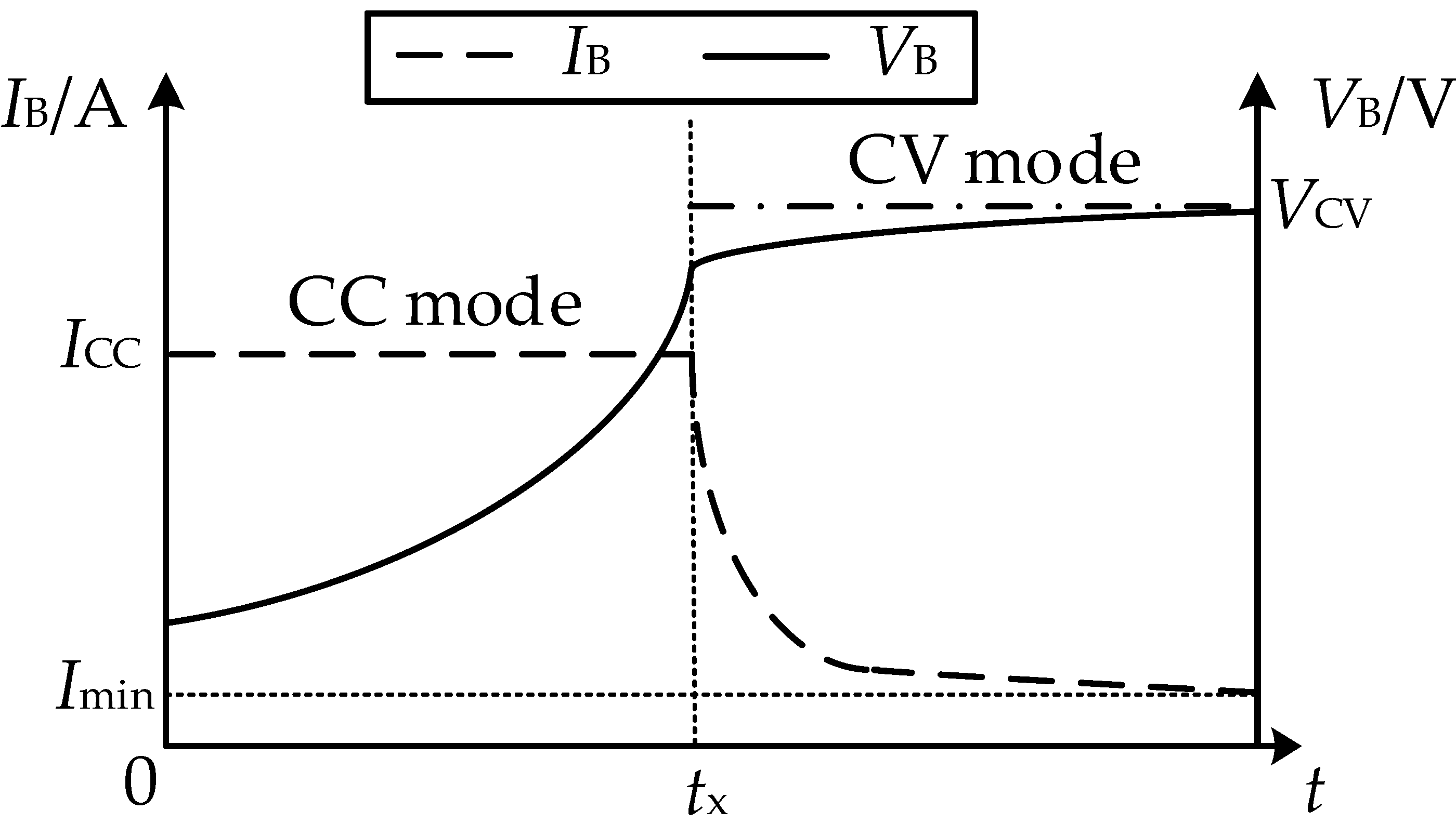
The constant-current and constant-voltage charging curves of a lithium-ion battery are shown in
Figure 2. Here, the
ICC is the charging current in CC mode, the
VCV is the charging voltage in CV mode, and the
Imin is the cut-off charging current. Moreover,
IB is the variation trend of the battery current, and
VB is the variation trend of the battery voltage.
The rest of this article is organized as follows. A novel single-switch hybrid compensation topology is proposed, and the compensation networks of the CC and CV modes are analyzed in
Section 2. In
Section 3, the equivalent input AC voltage is calculated theoretically, then the zero voltage switching (ZVS) margin is designed, and thereafter, the CC and CV gain curves and the sensitivity of circuit parameters are analyzed. In
Section 4, the magnetic coupler and circuit parameters are designed. An experimental prototype is built to verify the theoretical analysis in
Section 5. The output current is 4A in CC mode, and the output voltage is 48V in CV mode. In addition, the output characteristics of constant-current and constant-voltage modes are analyzed, respectively. Finally,
Section 6 concludes this article.
2. Analysis Compensation Network
As shown in
Figure 1,
Cp is the resonant capacitance at the primary-side. The primary side can be regarded as the P compensation network, where
Udc is the input DC voltage,
Q is MOSFET, and
Lp and
Ls are the self-inductances of the transmitting coil and receiving coil, respectively. In addition,
M is the mutual inductance between the two coils,
D1 –
D4 are four diodes to form the rectifier bridge,
Co is the output filter capacitor, and
RL is the DC output load. The secondary-side compensation network can be designed according to the requirements of the output.
When the compensation network of single-switch circuit is analyzed,
Figure 1 can be simplified as
Figure 3. Here,
is the equivalent AC voltage input to the compensation network, which is determined by the voltage waveform of
Cp. By applying Thévenin’s and Norton’s theorems,
Figure 3a can be simplified as
Figure 3b, and
LT =
Ls −
M2/
Lp is defined.
To realize the constant-current and constant-voltage output in the single-switch circuit, the hybrid P-LC and P-S compensation network can be designed as shown in
Figure 4a. When S
1 is connected to
Cs1, the circuit can be regarded as the P-LC compensation with constant-current output characteristics. However, the design freedom of the loosely coupled transformer (LCT) is not high. When S
2 is connected to
Cs2, the circuit can be regarded as the P-S compensation with constant-voltage output characteristics. In order to improve the design freedom of the loosely coupled transformer, as shown in
Figure 4b, the hybrid P-LCC and P-S compensation network is proposed.
Cs1 and
Cs2 can be used to adjust the output current in constant-current mode. The secondary side compensation network is changed by two switches S
1 and S
2. When both switches are turned on, the circuit is in constant-current mode, and the circuit can be regarded as the P-LCC compensation network. When both switches are turned off, and the circuit is in constant-voltage mode, the circuit can be regarded as the P-S compensation network.
The equivalent circuit in constant-current mode is shown in
Figure 5. Here,
is the output current of the compensation network. As shown in
Figure 5a, when switches S
1 and S
2 are turned on,
Cs1 and
Cs2 are connected in parallel, and the equivalent capacitance is defined as
CT. As shown in
Figure 5b,
LT1 and capacitor
CT are inductive after they are connected in series, and the equivalent inductance is defined as
LT1. In order to achieve the constant-current output, the equivalent inductance
LT1 and
Cs3 resonate at frequency
f. In this case,
Figure 5b can be simplified as
Figure 5c.
The equivalent model in constant-voltage mode is shown in
Figure 6. Here,
is the output voltage of the compensation network. In this mode, switches S
1 and S
2 are turned off, similarly, when the equivalent inductance
LT,
L1, and
Cs1 resonate at frequency
f. In this case,
Figure 6a can be simplified as
Figure 6b.
From
Figure 5, the following conditions should be satisfied in CC mode.
where
ω = 2
πf,
f = 1/
T,
f is the working frequency of the system,
T is the working period of the system. In constant-current mode, the output current can be expressed as:
It can be obtained from (2) that the output current in CC mode is independent of
L1, and the value of
CT can be adjusted to change the output current. In order to make the input impedance
ZT resistive in
Figure 5b, the relationship between
L1 and
Cs3 can be expressed as:
From
Figure 6, the following condition should be satisfied in CV mode:
The output voltage in CV mode can be expressed as:
A full-bridge diode rectifier and capacitor filter are used to rectify the AC output current and filter the ripple voltage. The relationship between the output DC load current
IL and the peak AC current
io before rectification is as follows:
where
E1 is the fundamental peak value of the equivalent input voltage source. The relationship between the output DC load voltage
VL and the peak AC voltage
vo before rectification is as follows:
The relationship between
RL and
Req is as follows:
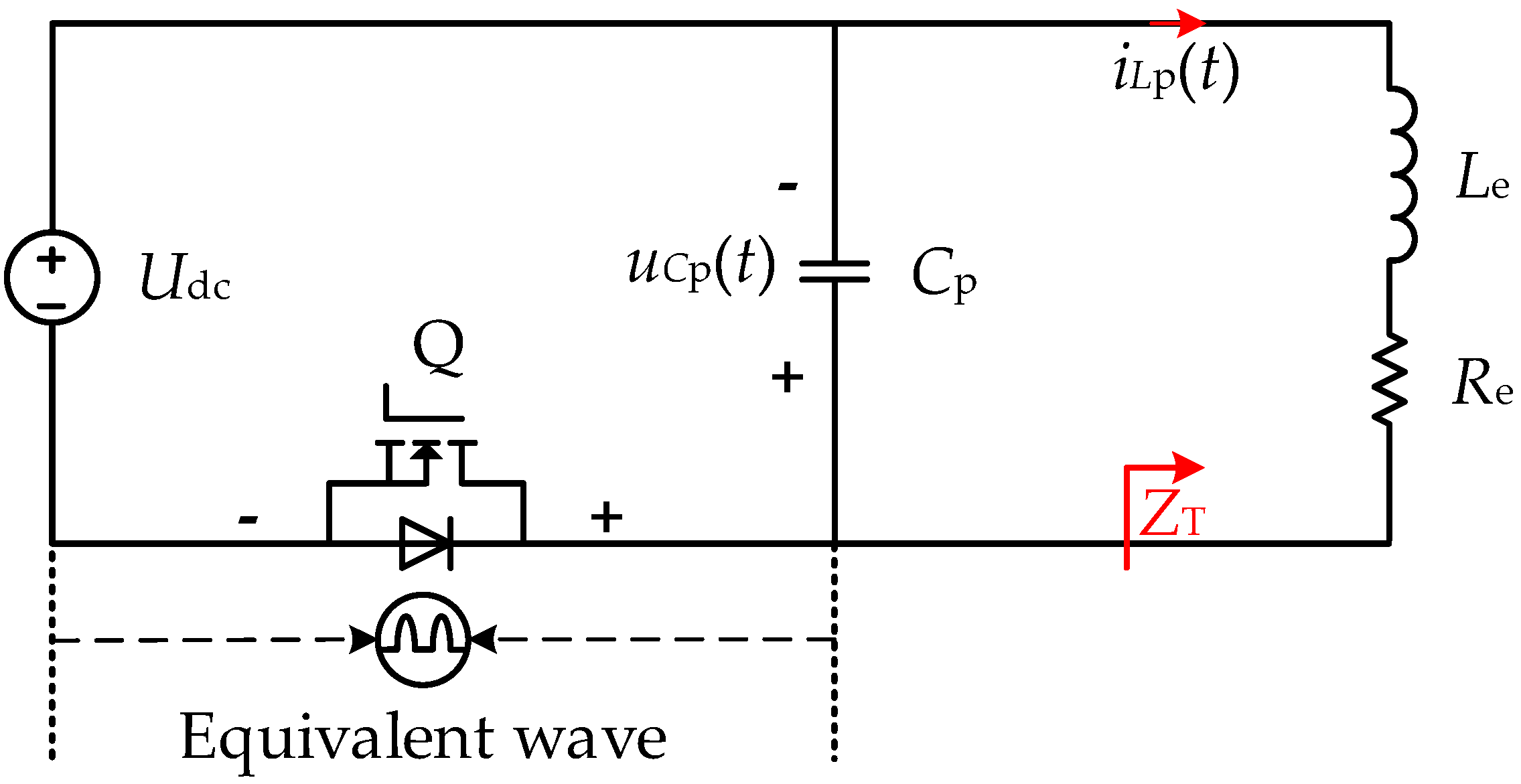
3. Calculation of Equivalent Input AC Voltage Source
For the single-switch circuit, the value of the AC voltage input to the compensation network is the voltage on the capacitor
Cp. However, the voltage waveform of
Cp is not a complete square wave. Here, the voltage waveform of
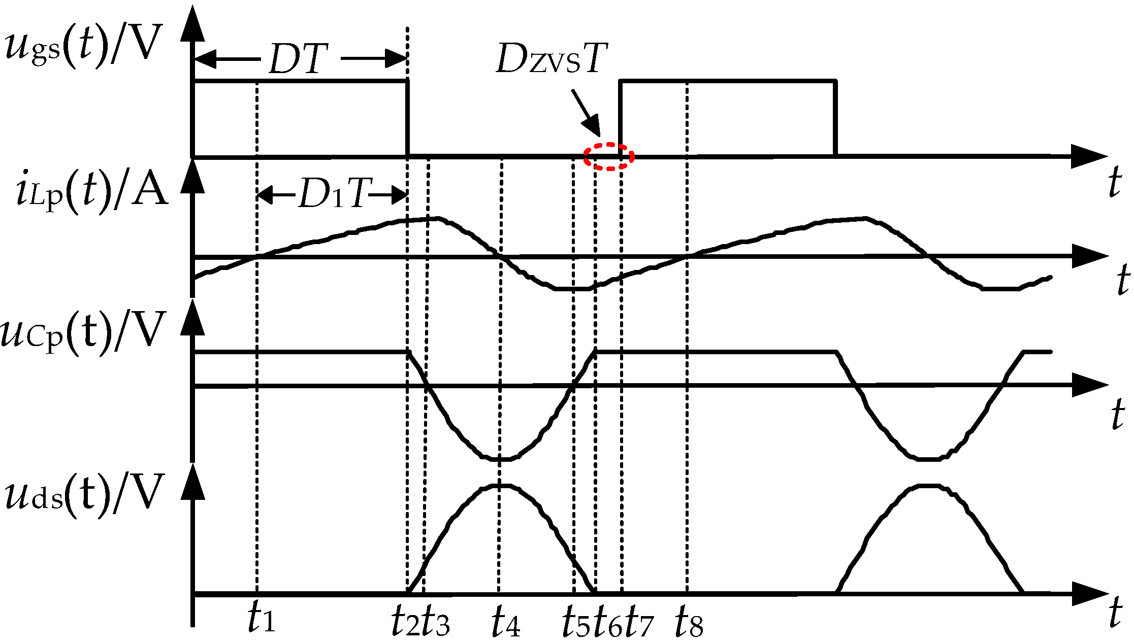
Cp is composed of a rectangular wave and half sine wave. It is necessary to calculate the equivalent AC voltage input to the compensation network. The relevant voltage and current waveforms are shown in
Figure 7. Here,
ugs is the driving signal of
Q,
iLp is the current of the transmitter, and
uCp is the voltage of the capacitor
Cp. In addition,
uds is the voltage stress on the switch
Q. The voltage waveform of
Cp in one operating period can be divided into three stages. During 0 to
t2, it is the conduction time of
Q, and
uCp is equal to the input DC voltage
Udc. During
t2 to
t6, it is the blocking period of
Q, and
uCp is determined by the compensation network. As shown in
Figure 8a, the waveform of
uCp can be regarded as the sine wave. During
t6 to
t7, there is a current flowing through the anti-parallel diode of
Q, which provides conditions for
Q to realize ZVS. Moreover,
uCp is equal to the input DC voltage
Udc, and the margin of ZVS is defined as
D1.
Since
Cp and the primary coil
Lp are in parallel,
uCp =
uLp,
uLp is the voltage of the primary coil
Lp, and the average voltage of inductor is zero in one operating period. As shown in
Figure 8, it is the waveform of
uLp, where
E is the maximum resonant voltage of
Cp, and the expression of
uLp in one operating period can be written as follows:
where
ω1 is the angular frequency of the sinusoidal half wave, and
ω1 can be expressed as follows:
Assuming Δ
t =
t3 −
t2 =
t6 −
t5, Δ
t can be expressed as follows:
As shown in
Figure 8a, the symbols
t3,
t5, and
t6 can be expressed as follows:
As shown in
Figure 8b,
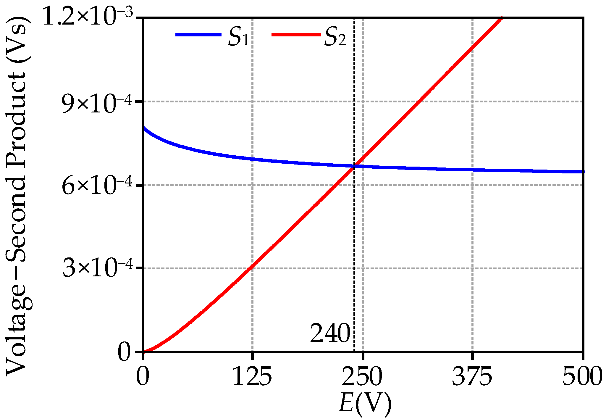
S1 represents the yellow area, and
S2 represents the blue area, using the principle of volt-second balance,
S1 =
S2,
S1 and
S2 can be expressed as follows:
In order to realize ZVS of
Q and improve the stability of the WPT system, setting the ZVS margin
DZVS = 5%, the duty cycle
D is fixed at 0.5. This paper sets the input DC voltage as
Udc = 96 V,
f = 85 kHz. Through the Mathcad software, the intersection of
S1 and
S2 can be obtained using Formula (12). As shown in
Figure 9, the intersection of
S1 and
S2 is 240 V, in other words,
E = 240 V. The above analysis provides a theoretical basis for the value of
Cp. According to the value of
E, the coefficients of Δ
t,
t3, and
t5 can also be obtained.
The peak voltage of
Q is the sum of the peak voltage of
Cp and the input DC voltage
Udc,
UQmax is the peak voltage of
Q, which can be expressed as:
The waveform of
uLp(
t) can be decomposed by Fourier decomposition to obtain the fundamental amplitude. The expansion of Fourier series of
uLp(
t) can be expressed as follows:
where
a0,
a1, and
b1 can be expressed as:
The expansion of Fourier series of
uLp(
t) can also be expressed as:
where
E0 =
a0,
,
.
E1 represents the fundamental amplitude, and
E0 represents the DC component.
For the single-switch circuit, when the duty cycle D is fixed, the values of
Cp are mainly used to adjust the ZVS margin. From
Figure 7, when the driving signal of
Q turns off at
t2, the
Cp,
Le, and
Re will have a zero input response, and the range values of
Cp can be determined from the perspective of energy attenuation. The simplified circuit model is shown in
Figure 10. Here, the reflected impedances from the secondary to the primary can be expressed as
ZT,
ZT =
jωLe +
Re.
From
Figure 10, it can be seen that
iLp(
t1) = 0, and the charging time of
Lp is equal to
D1T. It should be noted that
D1 ≤
D.
iLp(
t) can be expressed as:
At time
t2, the total energy stored by
Lp and
Cp can be expressed as:
At time
t4,
iLp = 0, the voltage value of
Cp rises to the maximum. The rate of energy attenuation is
, the time of energy attenuation is
.
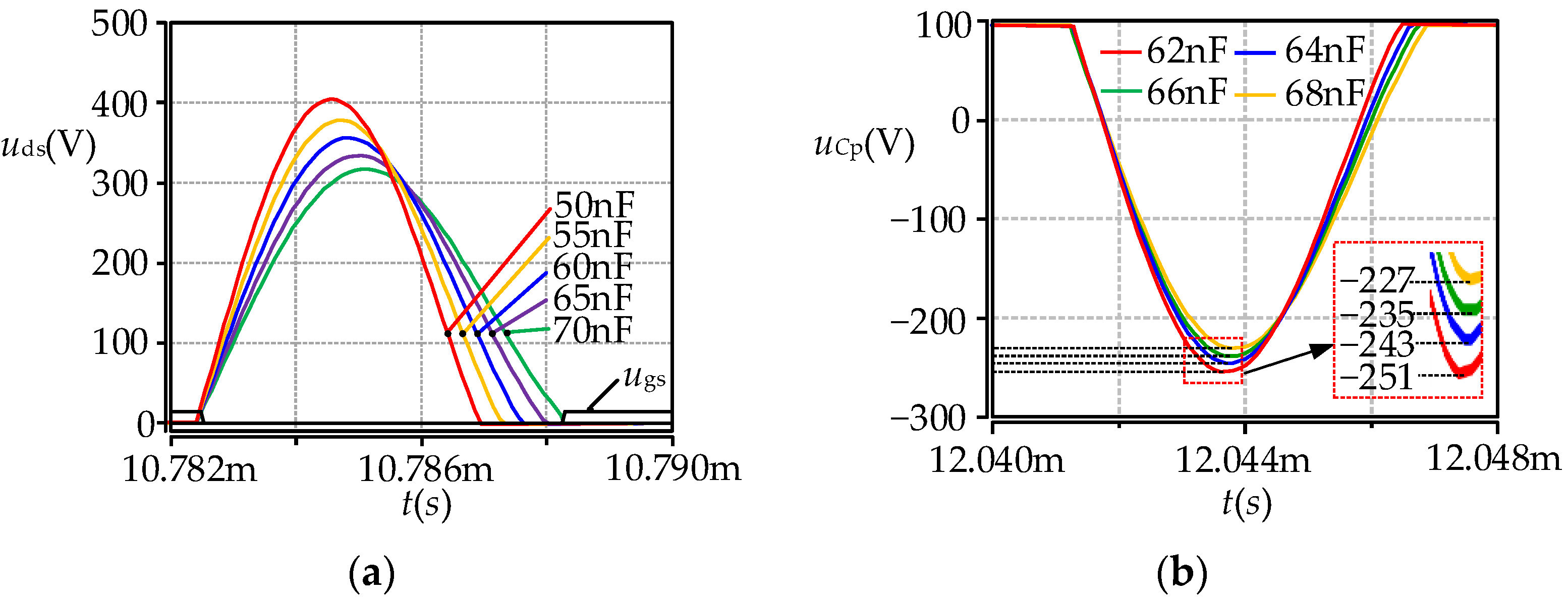
4. Simulation Verification
The waveforms of
uds and
uCp versus
Cp values in Saber simulation are shown in
Figure 11. It can be seen that with the increasing value of
Cp, the maximum value of
uds decreases gradually, and the ZVS margin
DZVS decreases until it disappears.
The theoretical calculation in
Section 3 provides the basis for the actual value of
Cp. When the input DC voltage is 96 V and the switching frequency
f is 85 kHz, in order to obtain a 5% ZVS margin, the peak voltage of
Cp should be about 240 V. As shown in
Figure 11b, when other circuit parameters are determined, the value of
Cp is changed continuously in Saber simulation until the value of
uCp is about 240 V, and
Cp = 64.5 nF. When
Cp = 64.5 nF, the ZVS margin measured in the simulation is about 5.5%, which is close to the design target of 5%, indicating that the calculation method is reliable in
Section 3.
As shown in
Figure 12, the fundamental amplitude after Fourier decomposition is 156.25 V, when
CP is set as 64.5 nF in Saber simulation. The fundamental amplitude after Fourier decomposition is 158.3 V by (17). The values of the calculation and the simulation results can match well, and thus, validate the correctness of the theoretical analysis in
Section 3.
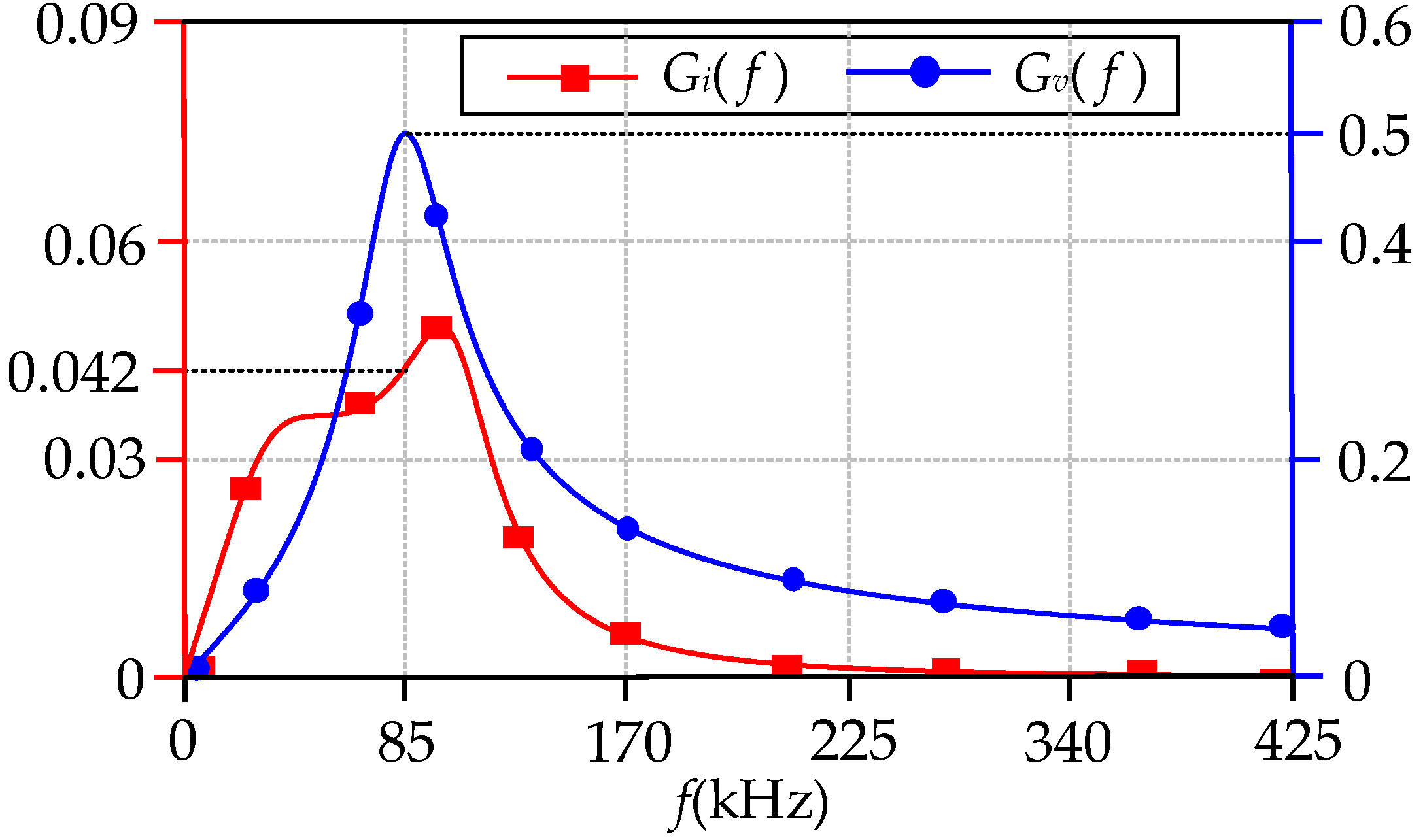
When all the circuit parameters are determined, the gain curve in the constant-current and constant-voltage modes can be drawn. As shown in
Figure 13, it is the current gain curve in constant-current mode and the voltage gain curve in constant-voltage mode. In addition, it can be seen that the current gain value
Gi(
f) at 85 kHz is 0.042, and the voltage gain value
Gv(
f) at 85 kHz is 0.50. This indicates that when the input DC voltage is 96 V and the driving frequency is 85 kHz, the output current is about 4A, and the output voltage is approximately 48 V.
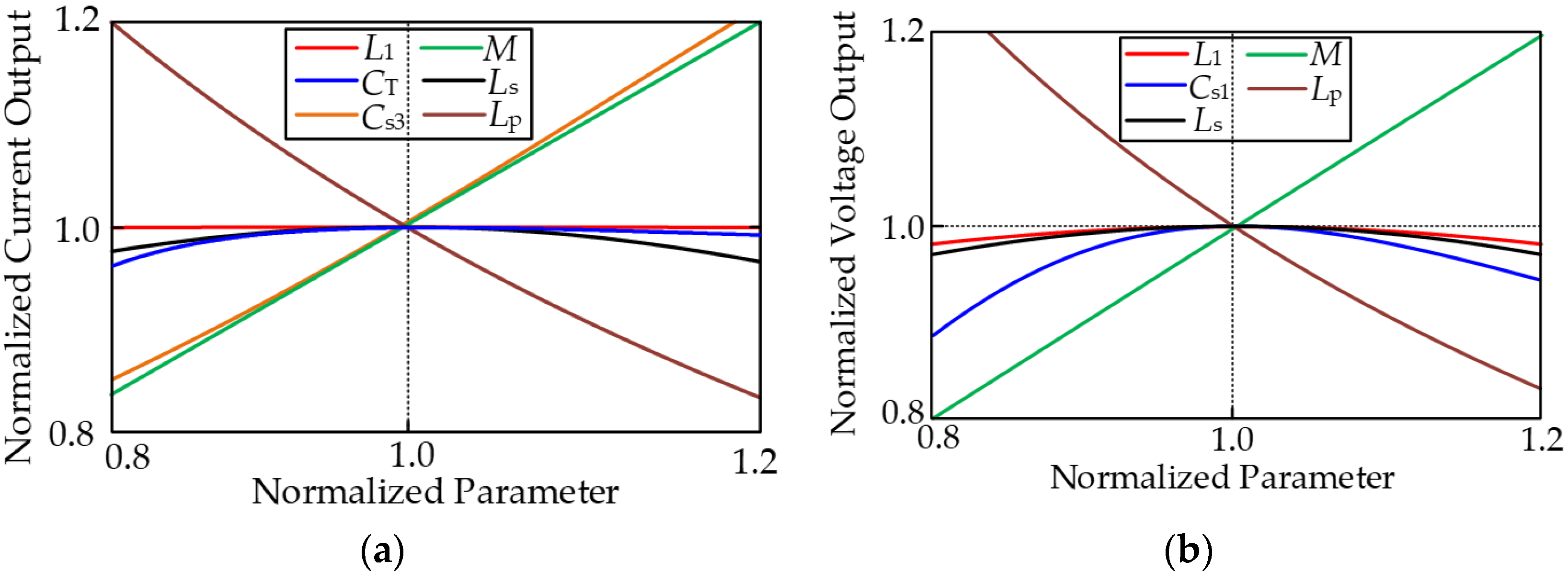
In order to analyze the influence of the components on the output current and voltage, the sensitivity of the circuit parameters is analyzed. As shown in
Figure 14, it is the normalized output with varying normalized parameters. In addition, it can be seen from
Figure 14a that
L1 has no effect on the output current in constant-current mode, and the values of
CT and
Cs3 can be used to adjust the output current. Therefore, the design freedom of the loosely coupled transformer is improved.
It can be seen from
Figure 14b that the variations of
L1 are not sensitive to the output voltage in constant-voltage mode.
As shown in
Figure 15, it is the composite shielding structure of magnetic coupler. The first layer of the shielding structure on the receiving coil side of the magnetic coupler is ferrite, the second layer is nanocrystalline strip, and the third layer is aluminium foil. As shown in
Figure 16, it is the cross-sectional magnetic flux density cloud images of different shielding structures.
The traditional shielding layer structure can be divided into two types, one is a single-layer shielding structure composed of ferrite, the other is a double-layer shielding structure composed of ferrite and aluminium plate. Compared with the double-layer shielding structure, the magnetic flux density in the air of single-layer shielding structure is higher. The double-layer shielding structure effectively reduces the magnetic field distribution in the non-working area, but the magnetic field in the working area is also reduced. The thickness of the iron-based nanocrystalline strip is 26 µm, the resistivity is 137 µΩ·cm, and the saturation magnetic induction is as high as 1.6 T.
In the composite shielding structure, the magnetic field in the non-working area above the receiving coil decreases and the magnetic field in the working area increases. For the double-layer shielding structure, the shielding effect at 240 mm outside of the magnetic coupler is increased by 14.85%, and the coupling coefficient is increased by 28.64%. When the composite shielding structure is adopted, the shielding effect at 240 mm outside of the magnetic coupler is increased by 20.32%, and the coupling coefficient is increased by 37.86%. The parameters of different types of shielding structures for receiving coil, are shown in
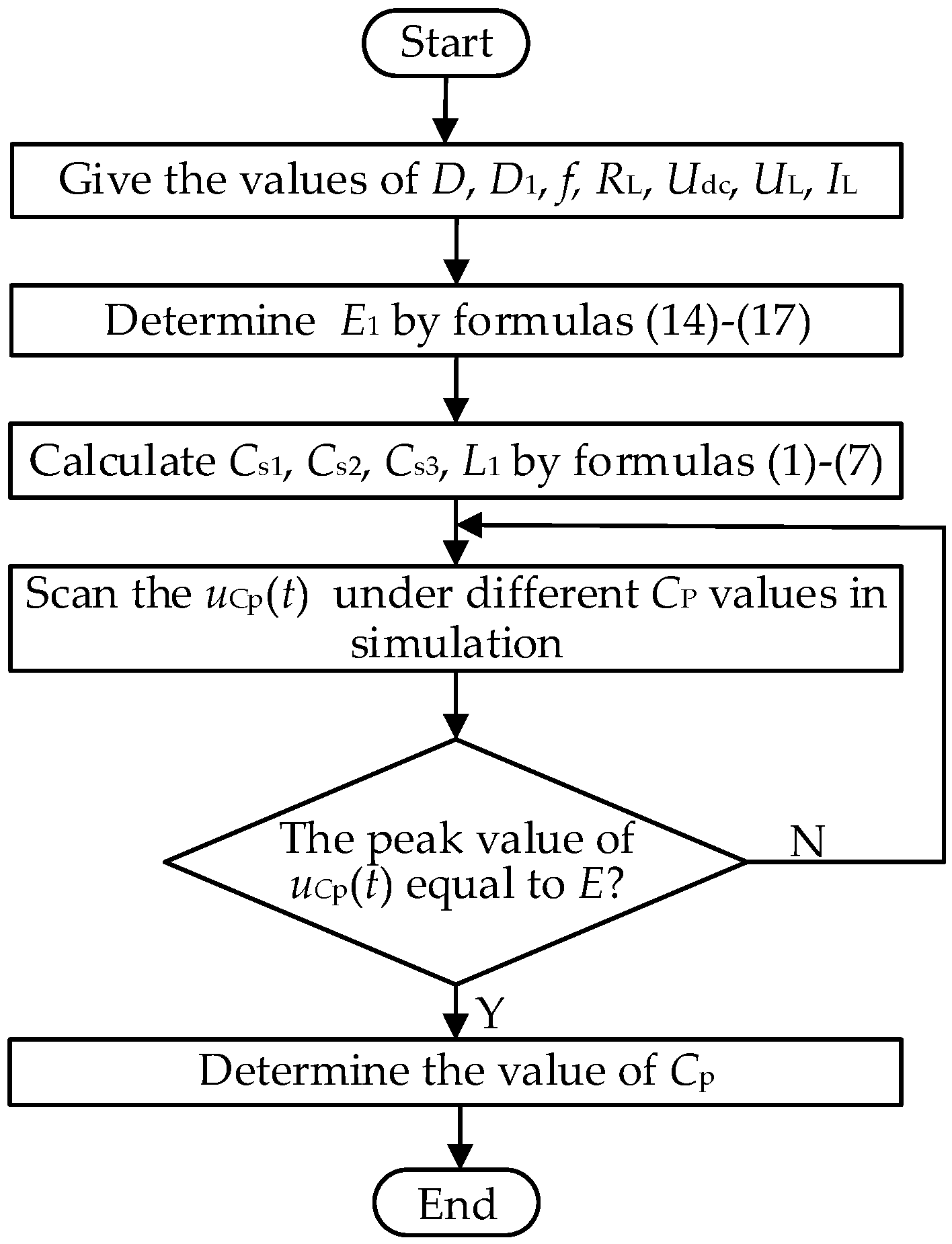
Table 1. Moreover, the flow chart of parameter design is shown in
Figure 17. As long as the values of self-inductance and mutual inductance are determined in the single-switch WPT system, the compensation network parameters can be designed according to the flow chart, and the method is universal.
5. Experimental Verification
The experimental platform is built through the experimental parameters in
Table 2, due to the variation of self-inductance and mutual inductance in different shielding structures. The values of compensation capacitances should be different, and the compensation network parameters given in
Table 2 are only designed on the basis of composite shielding structure. Here, it should be explained that the rated power experiment is only conducted in the composite shielding structure. Due to the changes of self-inductance and mutual inductance under other shielding structures, the output power will also change.
As shown in
Figure 18, the experimental platform mainly includes the primary circuit, secondary circuit, magnetic coupler, oscilloscope, and electronic load. The theoretical analysis can be verified through the experimental platform. Q is SiC MOSFET (CGE1M120080), and the secondary rectifier diodes are DPG30C300HB. The system is powered by a dc voltage source. Metallized polypropylene film capacitors (CBB) are used as compensation components. The STM32F103 is used to generate switching signals for the inverter. The transmitters and the receiver were wound using Litz wires. The mutual inductance and self-inductance were measured by the Agilent 4263B LCR meter. The rocker switches S
1 and S
2 are used to switch the compensation networks to achieve the constant-current output or constant-voltage output.
Due to the limitation of the experimental conditions, the battery is replaced by the electronic load as the load. The electronic load (IT8616) can be used to change the resistance load to verify the output characteristics of the proposed topology.
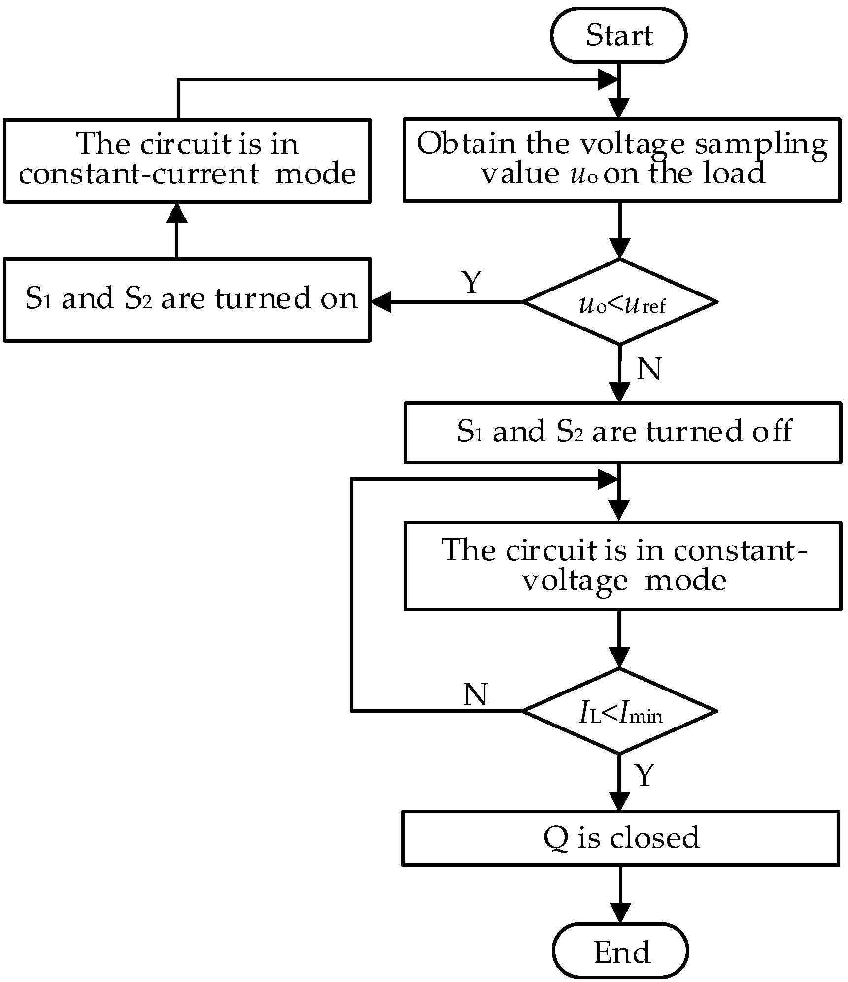
The control flowchart of the proposed WPT system for the CC and CV modes is shown in
Figure 19. Here,
uref is the critical reference voltage at the conversion point between the CC and CV modes and
Imin is the lower limit of the output current. When the sampling voltage
uo is lower than the reference value
uref, the switching signals are generated to drive the MOSFET (Q), and the system is then in the CC mode.
When the sampling value uo is higher than or equal to the reference value uref, the CV mode is selected. With the load RL increasing in CV mode, the output current decreases gradually. Considering the possible problems (high current or high voltage spikes) caused by the transition point, a switching method is proposed here to avoid the problems. A short period of time before and after the mode convention point, the PWM signal of Q is closed. Although it causes a short charging pause, for a few hours of the real charging process, this effect can be ignored.
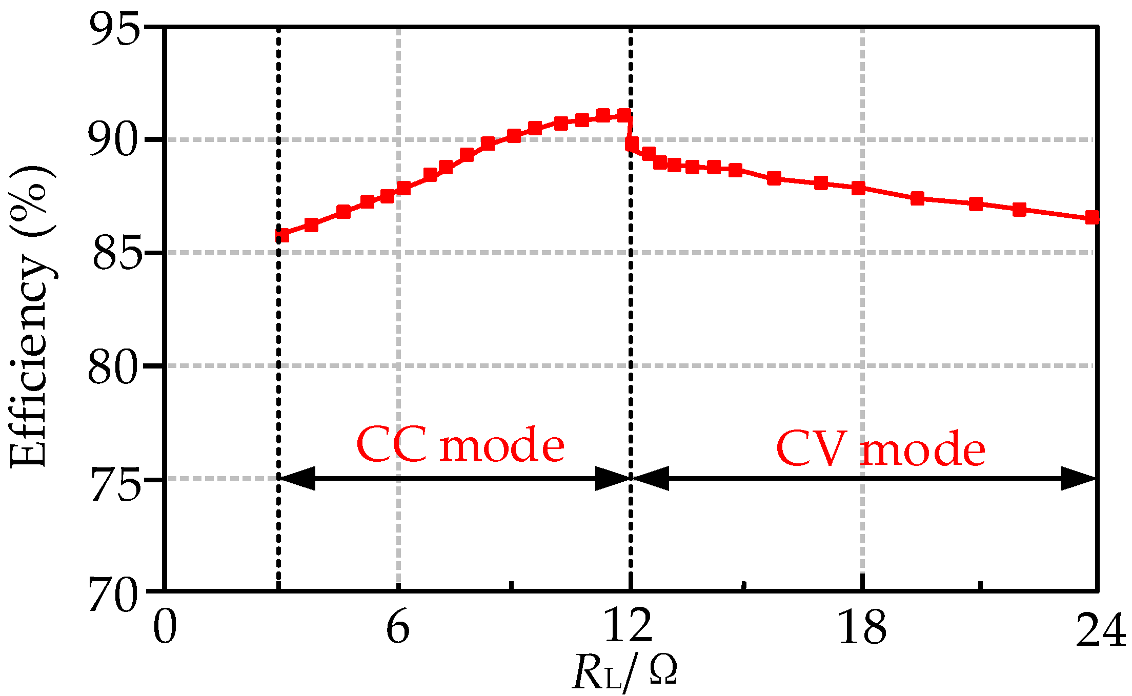
In the experiments, the variation of the load resistance is 6–12 Ω in constant-current mode, and the variation of the load resistance is 12–24 Ω in constant-voltage mode. In order to verify that ZVS can be realized in the experiments, the ZVS waveforms were measured under the minimum and maximum load conditions. From
Figure 20, the ZVS margin is 6.2% when
RL is set as 6 Ω, and the ZVS margin is 4.76% when
RL is set as 24 Ω. The design of ZVS margin ensures the ZVS of switch Q.
As shown in
Figure 21, the performance of the proposed WPT system is tested when the load is suddenly changed. In
Figure 21a,b, it can be found that the proposed WPT system can maintain a constant output current in the CC mode and a constant output voltage in the CV mode.
Figure 22 gives the measured output currents and voltages versus the load. As shown in
Figure 23, the maximum efficiency is 91.4% in CC mode, and the maximum efficiency is 90.2% in CV mode. As the current flowing through the coils increases when switching from the CC mode to the CV mode, the loss increases. Therefore, the efficiency sags at the mode transition.
As shown in
Table 3, the performance of the work in this paper is compared with other existing single-switch circuit based WPT. It can be seen that the proposed topology with the composite shielding structure can achieve higher efficiency.


