Communication

Analysis of the Photovoltaic Waste-Recycling Process in Polish Conditions—A Short Review

by
Renata Włodarczyk
Faculty of Infrastructure and Environment, Czestochowa University of Technology, J. H. Dabrowskiego Str. 69, 42-200 Czestochowa, Poland
Sustainability 2022, 14(8), 4739; https://doi.org/10.3390/su14084739
Submission received: 11 March 2022 / Revised: 9 April 2022 / Accepted: 11 April 2022 / Published: 15 April 2022
(This article belongs to the Section Sustainable Urban and Rural Development)

Abstract

:
The rapid development of the photovoltaic (PV) industry is determined by subsequent legal documents and directives, which indicate the need to use renewable energy sources in order to counteract climate pollution and strive to increase energy efficiency. The development of the photovoltaic industry in the near future will result in an increase in the amount of electrical and electronic waste from used photovoltaic panels. The total installed capacity of photovoltaic sources in Poland at the end of 2019 was almost 1500 MW, and in May 2020, it exceeded 1950 MW, and the weight of the installation was approximately 120,000 tons. The aim of the present work is to present the types of materials used in the construction of photovoltaic panels, with particular emphasis on the possibility of recycling or utilization of individual elements. Additionally, the aim of the work is to describe the most important requirements addressed to the members of the European Union, which were formulated in the provisions of Directive 2012/19/EU. Taking into account the number of photovoltaic panels produced in Poland, the possibility of recycling individual materials from PV assembly was analyzed. The author presents the problem of recycling in the combination of legal and material aspects, which will soon become the share of Poland as a member of the European Union.

1. Introduction

According to the data published by PPG (Polish Power Grids), as of 1 August 2020, the installed capacity in photovoltaic PV industry in the National Power Grids is 2261.347 MWp, and at the peak time, photovoltaic installations provides approximately 71% of the capacity, which is equivalent to a capacity of 1609 MW [1,2,3]. In April 2020, record-breaking daily electricity production was achieved so far, amounting to a total of 12.3 GWh. Electricity consumption is increasing, which results in an increase in the demand for its production. It is assumed that in Polish climatic conditions, an optimally located and constructed photovoltaic installation is able to produce a little over 1000 kWh per year from each. Photovoltaic installations make it possible to obtain clean and cheap electricity by converting energy from solar radiation into electricity. It is the photovoltaic modules, which are the most important element of the installation, that have the greatest impact on the efficiency of solar installations. The proper functioning of the installation depends on such important factors as correct assembly and setting and the type of link (type of material the link is made of). It should be borne in mind that, regardless of the installation issues, cells will produce the most energy in the summer months (April–September), even up to 70%, which will additionally depend on a given month and weather. Due to these factors, new materials are still being sought that enable the conversion of solar radiation into electricity using the photovoltaic effect.
Currently, the production of electricity from solar radiation, namely solar energy and wind energy, is the most important source of obtaining energy from renewable sources in Poland and in most EU countries. According to the National Energy and Climate Plan (NECP), the use of solar energy is an alternative to the use of brownfield sites and poor-quality land [4]. One of the ways to develop these lands is to install photovoltaic systems on them. PV installations, thanks to EU subsidies, are increasingly built in a dispersed manner on public utility buildings and private buildings. Regardless of the conditions and place of implementation of the investment based on renewable energy sources, the overall installed capacity will have an increasing impact on the functioning of the national energy system (NES). According to the Institute of Renewable Energy, until 2018, Polish companies supplied the market with about 50% of key devices (photovoltaic modules) and almost 100% of installation services [5]. However, already in 2019, the needs of the rapidly growing market began to be increasingly satisfied by foreign companies. This state of affairs is dictated by the requirements imposed on Poland by the EU, the 2016 Climate Package, and the latest documents, including Poland’s Energy Policy until 2040 [6]. The strategic document indicates that the key role in achieving the goals in the electricity sector in relation to RES (Renewably Energy Sector) will be the development of photovoltaics (mainly until 2022) as well as allowing energy recipients to generate and sell energy, i.e., to develop prosumer installations. According to the National Energy and Climate Plan for 2021–2030 [4,7], an important role in the development of renewable energy sources in the energy mix will be scientific research, innovation and competitiveness of the energy sector as part of R&D&I (research + development + implementation). Another strategic document, National Smart Specializations (NSS), takes into account the development of innovative technologies and industrial processes under NSS 11, including printed, organic, and flexible electronics with an indication of photovoltaics and other alternative energy sources and the production of flexible photovoltaic cells and others to power personal electronics and industrial.
The important role of electricity production in photovoltaic cells is highlighted in the following documents: Directions for the Development of Energy Innovation [8], plan for meeting the current and future electricity demand for 2021–2030 [9], and the strategy for responsible development until 2020 (with a perspective until 2030) [7]. Political guidelines for the next term of the European Commission (2019–2024)—“The Union that aims higher”—concern the reduction of emissions by 40% in 2030 and even by 50–55% by 2050 through the implementation of a responsible energy transformation of the member states [10]. The European Green Deal covers activities related to increasing resource efficiency, investing in environmentally friendly technologies, and supporting industrial innovation. The indicated actions are in line with the objectives of the “New Energy” Program, including the mainstream of achieving climate neutrality by 2030 in the European Union. The Strategic Energy Technology (SET) Plan [5] emphasizes that in the future, there will be even stronger development of technologies and innovations in the field of obtaining energy from renewable energy sources, especially PV technology.
National and international documents and assumptions indicate that photovoltaic technologies will still be developed in order to increase the efficiency of electricity production, and more solar power plants will be built on a larger scale [6]. This technology will face major challenges in terms of materials, durability, and efficiency. The aspect of utilization and recycling of individual elements of photovoltaic panels is also important.
Several European countries are already experiencing problems with the recycling and disposal of photovoltaic waste. In 2013, Italy produced PV installations of 17,620 MW, which was the result of all attractive support policies. Due to the development of this matter, after the end of the PV lifetime (approximately twenty to thirty years), there will be a problem in the replacement of PV systems. As a result of the consequent situation, the European Union adopted Directive 2012/19/EU [11], which extends the scope of electrowaste to include used photovoltaic panels as large-sized equipment that, after appropriate segregation, can be recycled and/or utilized. The directive is addressed to all member states of the European Union. The directive aims to facilitate the collection, reuse, and recycling of used materials and electronic devices and their records, which is to contribute to the reduction of the amount of waste and the efficient use of resources and to prevent illegal exports of such waste from the EU, with the benefit of the environmental performance of all entities involved in product life cycle from device manufacturers, distributors, and consumers. In Annex II of the Directive, in the exemplary list of electrical and electronic equipment (EEE), photovoltaic panels, belonging to the category of large-scale equipment with external dimensions exceeding 50 cm, are indicated.
The intensive development of the photovoltaic industry in Poland and in the world already generates an increase in the amount of electrical and electronic waste from used photovoltaic panels. The total installed capacity of photovoltaic sources in Poland at the end of 2019 was almost 1500 MW, and in May 2020, it exceeded 1950 MW. The mass of the installed installations amounted to approximately 120,000 tons. The article presents the types of materials used in the construction of photovoltaic panels, taking into account the possibility of recycling or utilization of individual elements. The most important requirements addressed to the members of the European Union, which were formulated in the provisions of Directive 2012/19/EU, are described. The possibility of recycling individual materials from PV assembly was analyzed taking into account the type and mass content of elements, and the basic processes used for recycling or utilization of these materials are presented. The article analyzes the possibilities of recovering materials and recycling materials used in the construction of various types of photovoltaic panels, supported by examples of the use of thermal and chemical treatment. There is still a problem related to the presence of heavy metals in PV materials and the risk of their distribution to the environment. The market of PV technology in Poland and the approach to the future need to use the panels used were analyzed.
The lifetime of photovoltaic panels is estimated at 20–35 years. The rapid development of renewable energy shows that 41.8 million metric tons of PV panels are produced each year, which constitutes 0.6% of total e-waste. Even more end-of-life panels will be generated in the future. In the legislative aspect, the European Union has the best-designed legal framework for the management of photovoltaic waste. The WEEE directive [11], which was published in 2003, only concerned e-waste. Reality has verified the requirements, and in 2015, requirements for the collection and recycling of photovoltaics entered Germany. The Stiftung EAR department is tasked with registering e-waste but is not responsible for collection, treatment, dismantling, and recycling. These procedures are governed by the Electrical and Electronic Equipment Act 2005 [12].

2. Materials for Photovoltaics Cell Technology

The quantity of materials sent for recycling and utilized should be assessed after analyzing the quality of photovoltaic panels, taking into account available technologies. The photovoltaic system consists of many components, including cells, which are connected in series with small modules, 2 electrical and mechanical connectors and connections, and adjustment tools that control and/or modify the output power, i.e., electricity [13,14]. The inverter is the most important component of a photovoltaic system [15]. Panels made of semiconductor materials, most often silicon, are equally important, as they can affect the efficiency of photovoltaics. Sunlight can turn into electricity thanks to this effect, which was discovered by the French scientist Becquerel. When photon rays of different wavelengths strike a solar cell, they can be reflected or absorbed by the absorbing material. Photon absorption generates an electron-hole pair that, when separated from the second junction, generates a voltage. Depending on the dielectric constant that characterizes an ordinary inorganic semiconductor (such as Si, Ga, As, and others, including a perovskite semiconductor), it does not need a junction for the electron-separation of a pair of holes. We call these Wannier–Mott excitons: the electron and the hole are at distances of many lattice constants, and the exciton’s wave function is delocalized. Compared to Frenkel excitons, the electron-hole pair is located at a lattice constant distance, and the exciton’s motion occurs through the hopping mechanism. As a result of the voltage, a current is created that flows through the external circuit. There are many types of solar cells, but more than 80% of those currently produced worldwide are made of crystalline silicon. The scope of current technologies and possible future options is as follows:
First generation: crystalline silicon (c-Si)
(a)
Monocrystalline;
(b)
Polycrystalline;
(c)
Ribbon sheets.
First-generation photovoltaic cells are photovoltaic cells made of crystalline silicon wafers. Silicon is a cheap and widely available semiconductor material characterized by high strength of crystal structures, relatively low toxicity, and good properties related to the conversion of energy from solar radiation to electricity (which is due to a well-matched energy band gap) [16,17,18].
(a)
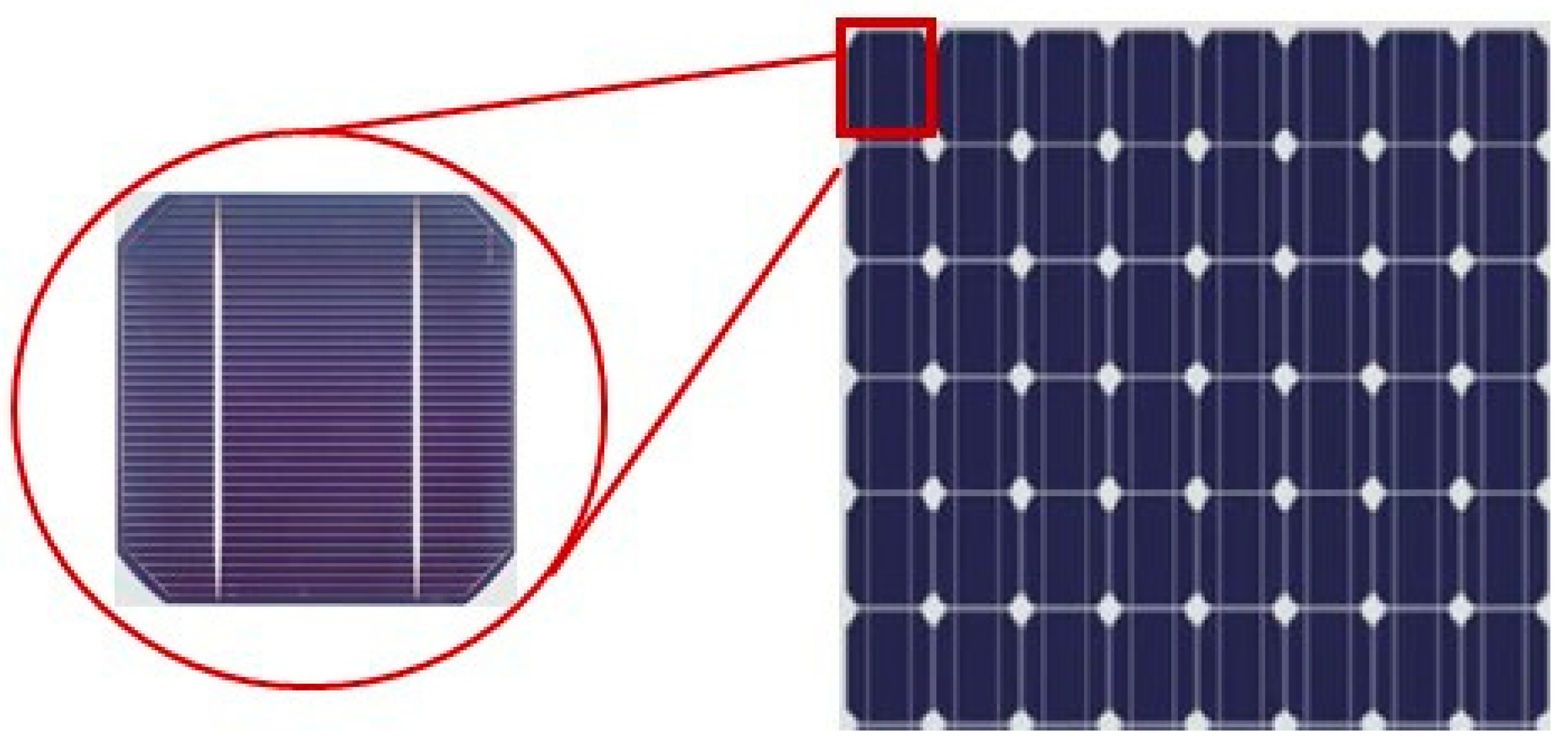
Monocrystalline cells are made of a single crystal of silicon having an ordered structure, which can be obtained from the crystallization process from each of the solid, liquid, or gas phases [19]. A single silicon crystal, after the production of a monocrystalline cell, acquires a dark blue color, with cut or rounded corners (Figure 1). Monocrystalline cells are characterized by high efficiency (usually about 18–22%) and durability, which entails high production costs. Photovoltaic panels made of monocrystalline cells have a moderate indicator of power decrease with increasing temperature as well as an increase in power with decreasing temperature in which the solar installation operates. Monocrystalline panels work best in conditions of strong sunlight or low ambient temperatures; any drops in insolation and an increase in ambient temperature significantly reduce the efficiency of cells made of monocrystalline silicon [20].
(b)
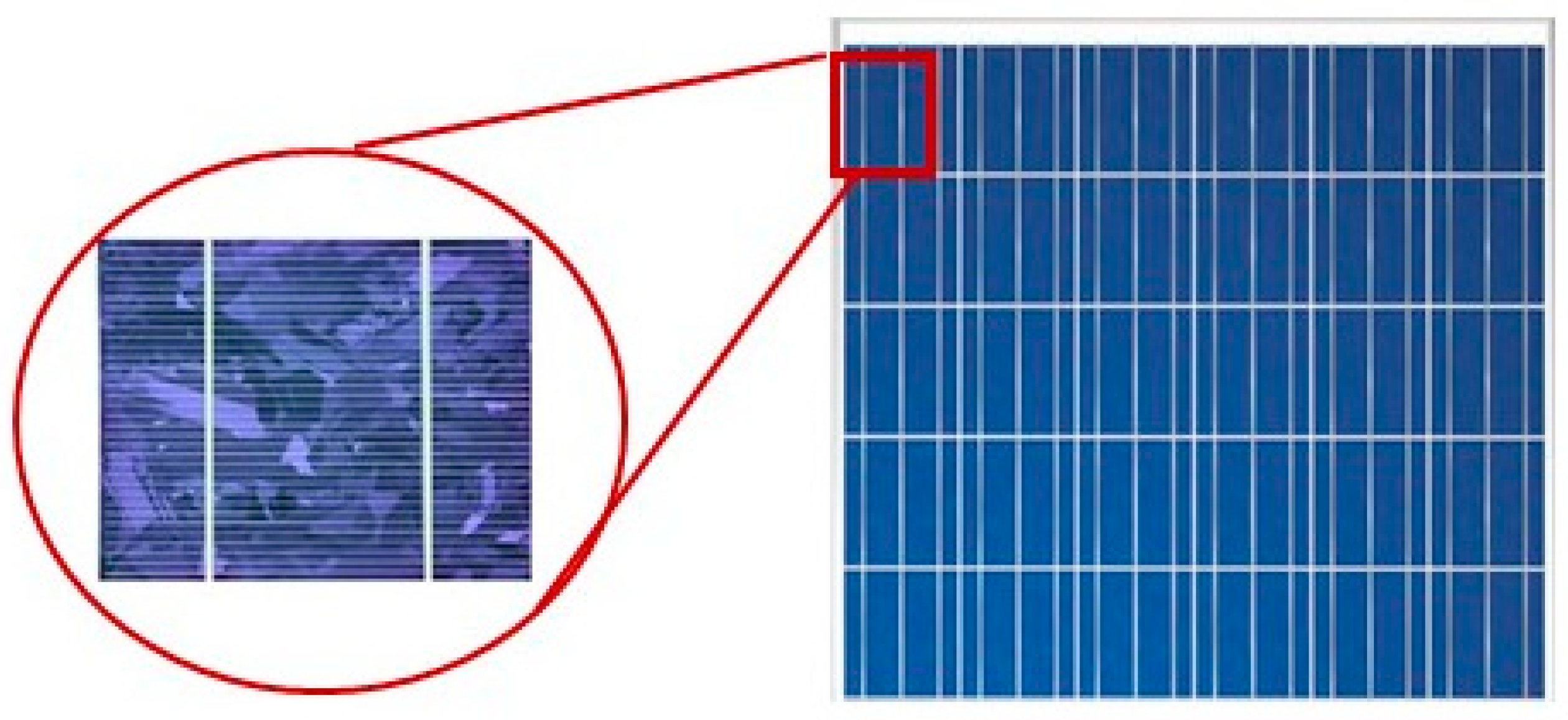
Polycrystalline cells are made of polycrystalline silicon plates of an irregular shape. Polycrystalline silicon is produced from crushed silicon crystals that are melted and then cast in the form of a cuboid, cooling and cutting into plates of appropriate thickness [19]. Due to the technology of producing polycrystalline cells, they usually have a blue color and clearly defined crystal edges (Figure 2). Polycrystalline cells are characterized by quite high efficiency, ranging from 14–18%. Photovoltaic panels made of polycrystalline cells are characterized by an efficiency lower than that of a monocrystalline module and a high rate of power drop with increasing temperature, usually lower than a mono module. Photovoltaic modules made of polycrystalline cells can withstand weather fluctuations and drops in sunlight much better than cells made of single crystal. Taking into account the price of photovoltaic panels made of polycrystalline cells, which are cheaper than monocrystalline ones per watt of installed power by about 8–15%, and the fact that polycrystalline cells perform much better in average weather conditions, they are much more popular than monocrystalline photovoltaic panels. The low price of these modules is influenced by the low production costs of polycrystals [20]. An alternative to silicon wafers are crystalline silicon ribbons, the production of which is based on wafers from ingots. Ribbon technologies are characterized by the fact that the wafers are crystallized directly from the molten material to the desired thickness, and there are no losses in the gaps. Consequently, they offer a high potential to significantly reduce the cost of PV energy compared to ingot wafer technology [21].
Second generation: Thin film
(a)
Amorphous silicon (a-Si);
(b)
Cadmium telluride (CdTe);
(c)
Multi-junction cells (a-Si-μc Si);
(d)
Copper indium gallium (di)selenide (CIGS), copper indium (di)selenide (CIS).
Second generation photovoltaic cells are made with the use of the latest technology of material processing and production. These materials are characterized by a thickness of the semiconductor layer from 1 to 3 μm; hence, they are called thin-film cells. Compared to the first-generation photovoltaic cells, thin-film cells are not produced on the basis of crystalline silicon but with the use of various types of materials such as amorphous silicon, cadmium telluride or mixtures of copper, indium, gallium, and selenium. Despite the use of specific materials for the production of the second generation cells, the cost of their production is low, and the technologies used allow for large material savings and a significant reduction in semiconductor consumption. These cells show much lower efficiency and achieved power compared to the cells described above [24,25].
(a)
Amorphous silicon cells (a-Si) consist of a very thin layer of non-crystallized silicon in a shapeless form, which is deposited on a substrate made of another material, such as glass, ceramics, plastic, or stainless steel (Figure 3a). The production technology of amorphous silicon cells is simple and allows to save a large amount of electricity and materials and also makes it possible to obtain cells with a large surface without having to cut them into plates. Amorphous silicon cells are characterized by low efficiency even for thin-film cells (efficiency in the range of 6–10%), low price, slight burgundy color, and complete absence of visible silicon crystals. Photovoltaic panels made of amorphous silicon cells do not lose their efficiency even on cloudy days. The advantage of amorphous modules is a very low power drop with increasing temperature; for this reason, hybrid modules are often used instead of them and based on combined amorphous and microcrystalline silicon cells [26,27].
(b)
Cadmium telluride (CdTe) cells are thin-film cells made of cadmium telluride, which is a semiconductor, deposited on a glass substrate (Figure 3b). Their characteristic feature is the fact that the cadmium compound used in the production of cells allows the creation of an entire photovoltaic panel using a single cell. Cadmium telluride cells have a fairly high efficiency for thin-film cells (oscillating between 10–14%) and are characterized by a black color. These cells are often used in the production of flexible photovoltaic panels that can be easily adapted to the building facade [28].
(c)
Multi-junction cells (a-Si-μc Si) are tandem solar cells that consist of amorphous and microcrystalline silicon junctions. The latest research concerns the study of new joint patterns as a two-dimensional photonic crystal. Such innovative solutions increase the efficiency of light conversion by more than 20% compared to conventional planar configurations [29].
(d)
Cells made of indium-copper (di)selenide (CIS) and gallium (CIGS) are made of a semiconductor material consisting of a mixture of copper-indium (di)selenide, for CIS (chemical formula CuIn1-xSe2), or of copper-indium-gallium (di)selenium (chemical formula Cu(In1-xGax)Se2 (Figure 3c)). The possibility of using four types of elements allows to increase the efficiency of the cells by increasing the scope of absorption of solar radiation. The efficiency of CIS/CIGS cells is slightly higher than that of CdTe cells (they range between 12–16%). As in the case of CdTe cells, the technology used to produce CIS/CIGS cells allows for the creation of an entire photovoltaic panel with a single cell [30].
Figure 3. View of materials used in the production of second-generation photovoltaic cells: (a) amorphous silicon; (b) cadmium telluride (CdTe); and (c) CIGS (copper indium gallium diselenide) Adapted from [31].
Sustainability 14 04739 g003
Third generation: Concentrator photovoltaic (CPV) and emerging technologies
(a)
Dye-sensitized solar cells;
(b)
Organic solar cells;
(c)
Perovskite cells;
(d)
Quantum dot cells;
(e)
PERC (passivated emitter and rear cell) and PERL (passivated emitter and rear locally diffused).
Third-generation photovoltaic cells are solar cells that are potentially capable of exceeding the Shockley–Queisser limit of 31–41% energy efficiency for solar cells with a single gap. Popular third-generation systems include multi-layer (“tandem”) cells made of amorphous silicon or gallium arsenide, while more theoretical developments include frequency conversion, hot carrier effects, and other multi-carrier ejection techniques. Third-generation cells are dye cells without P-N semiconductor junctions. Built on the basis of polymers and dyes, they are based on the phenomenon of photosynthesis. These cells are composed of nanocells that contain a synthetic dye that resembles chlorophyll to some extent. The process of converting energy from solar radiation into electricity is characteristic of each type of cell. Third-generation photovoltaic cells are characterized by high flexibility and lightness. Perovskites are as efficient as silicon cells. These cells, especially perovskites, are less sensitive to different angles of incidence in relation to the angle of incidence of light, which significantly exceeds the delicacy and sensitivity of silicon cells to these factors. An extremely important advantage of perovskite cells for the future development of technology is the method of their production, which makes them cheap [32]. Figure 4 shows the polymer cells belonging to the third-generation photovoltaic cells.
(a)
Dye solar cell/dye-sensitized solar cell (DSC/DSSC) has a relatively simple structure. The cell consists of an anode and a cathode with an electrolyte between them. The anode is a glass plate covered with a transparent conductive oxide (TCO) layer. Indium tin oxide (ITO) or fluorine-doped tin oxide are most commonly used. A thin layer of titanium dioxide (TiO2) is applied to the foil. The anode is soaked in a dye solution that binds to TiO2. The DSC cathode is a glass plate with a thin layer of Pt as catalyst. The electrolyte is an iodide/triiodide solution. Both electrodes are pressed against each other and sealed so that the cell does not leak. An external load may be energized as light strikes the anode of a dye solar cell. These cells can be printed on transparent surfaces, such as windows, transparent walls, or skylights, and then work on both sides in conditions where other types of photovoltaic cells would be useless. Dye cells can be divided into organic and inorganic ones, and they use photosynthesis to convert energy from solar radiation to electricity. Dye cells have quite a good price/performance ratio (efficiency in laboratory conditions is up to 13%) [34,35,36]. To improve the electrical conductivity and light capture in the back layers, the conductive crystal is most often indium-doped tin oxide (ITO) and zinc oxide doped with fluoride (FTO). The semiconductor electrode is usually a thin layer (~5–30 m) layer of nanocrystalline titanium dioxide (TiO2), the porous structure of which facilitates the deposition of the dye on the surface. DSSCs operate in low-light conditions. This type of cells is ideal for low-density applications, such as rooftop solar collectors, where the mechanical strength and light weight of the glassless collector is a great advantage because the thin, conductive material allows for quick heat dissipation. The disadvantage is the need to use a liquid electrolyte, which may freeze at low temperatures. An additional disadvantage is that the electrolyte solution contains organic compounds that are toxic to human health and the environment. Recently, progress has been made in the field of materials and the use of materials such as ruthenium compounds, quantum dots, natural dyes, and organic compounds excluding metals [37].
(b)
Organic cells’ structure is based on organic materials that include, among others, polymers (or macromolecules) and small molecules. Organic photovoltaic cells is a rapidly developing photovoltaic technology that improves cell efficiency up to 18.2%, with a long service life of over 10 years without encapsulation [31]. Despite their drawbacks, these cells are cheap, flexible, and lightweight [38,39].
(c)
A perovskite solar cell is a type of solar cell containing a perovskite structural compound, most commonly a hybrid organic–inorganic lead or tin halide-based material, as the active light-collecting layer. Perovskite materials such as methylammonium lead halides are cheap and relatively simple to manufacture. Perovskite cells are printed on PET film, thanks to which they are thin, light, flexible, and efficient; they can be used in places that do not have perfect lighting and in the interiors of buildings with artificial lighting. A compound with a perovskite structure is used as an active layer that is sandwiched between an electron transporting layer (usually mesoporous) and a hole transport layer. Perovskite cells are easy to manufacture, and their high water absorption coefficient allows them to absorb the entire visible solar spectrum with ultra-thin layers (~500 nm) [40]. These cells are unstable in the environment of moisture and oxygen; they are brittle and not very resistant to heat. The absorbing material dissolves in water, which leads to the degradation of the cells. To counter this, it is necessary to encapsulate the perovskite absorber, for example, in a composite of carbon nanotubes [41]. The highest efficiency of perovskite cells (21.1–21.6%) was obtained by mixing various cations to create perovskite structure: rubidium, cesium, lead, tin, germanium, and anions that can optimize the solar spectra, namely chloride, bromide, and rhodium anions [42,43]
(d)
Quantum dot cells (QDs) are nanoscale semiconductor materials belonging to groups II–VI, III–V, or IV–VI of the periodic table of the elements, which have a discrete spectrum of quantized energy because motion electrons and holes are limited. Due to the nanoscale dimensions, usually in the range of 2–10 nm [44,45], they show properties intermediate between mass semiconductors and discrete atoms or particles. In the QD structure, we can distinguish a core in which there are layers of various compounds. It is also possible to embed the QD in a die made of a different material. The QD concentration affects the yield of the material, and the addition of nanoparticles can even improve the yield up to 40% depending on the concentration of nanodots. The advantages of CPV based on QDs include a favorable power-to-weight ratio, savings in weight and space, low energy consumption, and versatile use. Some of the QDs can be toxic (CdSe) and require a protective coating and are difficult to size controlling.
(e)
As regards PERC (passivated emitter and rear cell) and PERL (passivated emitter and rear locally diffused), the first high-performance PERC cells were produced in 1988, with the efficiency of 21.8% confirmed in Sandia in October 1988 (20.9% according to the applicable standards) [46]. As can be seen from the general data of patent H01L31/02168 [46], the invention discloses a method of preparing a PERC solar cell: a passivated film is placed locally on the back of a silicon chip by screen printing to form a back passivation layer with specific patterns. The material performance is influenced by the method of fiber preparation, the process of back-polishing and etching, and then decontamination of the glass. For the production of PERC, the method of local screen printing of alumina foil or silicon oxide foil on the back of the silicon chip is used, thermal treatment is carried out, and then, the anti-reflective silicon oxide face is deposited.

3. Production and Market of Individual Photovoltaic Panels

Using the above information, Table 1 summarizes the characteristics and efficiency of all the discussed photovoltaic cells. In order to compile information on the type of materials used in the construction of photovoltaic cells and their structure, Table 1 has been developed [34,35,36,37]. After its analysis, it can be concluded that silicon is the most popular material used in the construction of photovoltaic cells. The breakdown of the shares of individual technologies in the global market of photovoltaic panels is presented in Table 1. The data show that panels made of mono- and post-crystalline silicon have the largest share, followed by panels using amorphous silicon [47,48].
The production and assembly of installations based on the operation of photovoltaic modules are one of the most dynamically developing branches of renewable energy. In the last decade, a significant increase in interest in photovoltaic panels can be observed, which results in the emergence of many competing companies involved in the production of PV panels and the production of new materials and methods that will allow obtaining photovoltaic panels with even higher energy efficiency at reduced production costs. Therefore, the market for PV modules is growing rapidly, which means more waste generated from the PV module and thus a greater scope of disposal and improvement of recycling processes. In fact, the number of PV modules reaching their service life has increased dramatically in the last decade [11,20,22]. Unlike other industries, the PV industry is unique because of the long lifetime of these components. A solar module usually lasts for 20–25 years. The main factors in determining the service life of photovoltaic modules are decomposition of ethylene vinyl acetate (EVA) copolymer under the influence of sunlight and deterioration of internal materials by external effects, such as toughened glass cracking and laminated PV cell defects. Currently, most damaged or used photovoltaic modules have been thrown away and buried underground without being recycled. The photovoltaic module can contain hazardous substances, such as Pb, Cd, Cr, and Bi, the presence of which causes serious diseases in humans and animals [49,50,51,52,53].
Knowing the composition and material content of modules, it is possible to determine the quality of waste depending on the type of PV module. Table 2 shows the average contents of individual elements and materials for the most important types of PV modules. Conventional silicon modules consist of materials such as copper (1%—connections), silicon (5%—solar cells), aluminum (8%—frames), polymers or plastics (10%—encapsulation l), and glass (76%—module surface). Glass, as a transparent material, protects against scratching and against overheating of the module.
In order to protect the modules against corrosion or contamination, air-tight sealing is used, most often with the use of EVA foil as well as Teflon or organic resins (Figure 5). Hermetic closure of the modules guarantees their high durability. As a result of the described works, a multi-layer structure of the module is created: glass/foil/EVA/cells/EVA foil/electro-insulating foil or glass. The back outer layer, called the substrate, prevents the negative effects of moisture and corrosion of electrical connections. The finished module is placed in an aluminum housing. Since silicon has a high light reflectance (30–55%), reducing this index and increasing the degree of solar radiation absorption, an anti-reflective coating is used. This coating is usually made of compounds such as SiO, SiO2, Si3N4, and Al2O3. Then, metal electrodes made of Ag, Cu, and Sn are most often used on the front of the panel [55]. The diversified composition of thin-film modules makes it difficult to recycle or utilize materials.

4. Recycling Process of Photovoltaic Panels

According to recent studies, it has been shown that recycling PV modules brings significant economic and environmental benefits with the implementation of appropriate recycling rules and their strict compliance [37]. In total, 90% of the solar cell production market is the production of crystalline silicon modules. It is the most widespread due to its low production cost and high efficiency. Additionally, the production cost and the production cost of a PV cell is 60% of the total cost of a PV module. Overall, 40% of the silicon element is lost when processing a silicon cell. Recently, silicon recycling technology has enabled the recovery of 60% of silicon from the waste PV module, but it is still too low a recovery percentage.
In the context of future assumptions related to the intensity of designed PV installations, it is very important to enable a circular economy for solar photovoltaic system materials [56]. Soon, the number of replaced modules will also increase due to the decline in their efficiency. Poland imports models and relies entirely on silicon imports. Industry stakeholders are considering sustainable management solutions and identifying barriers to the circular economy for PV materials. Moving from the degradative model of “take, produce, consume, dispose “, to the circular model will ensure longer life, high efficiency, and reuse/recovery of products and materials [57]. Authors [58] describe circular activities in line with the ReSOLVE framework. This analysis is product-oriented in a product and service system. The results show that in the case of PV installations, the most important aspects relate to servicing, repair, insurance, and warranty. Additional activities to enrich the circular model are of a conceptual and pilot nature.
Elemental silicon used in the production of semiconductor devices is made of high-purity quartz and quartzite sands. Quartzite sands are treated in an electric arc furnace, and as a result, its purity is 98% [59,60]. After this process, the silicon is further processed with grinding in a ball mill (75% < 40 μm) and treatment in a fluidized bed reactor, which produces 90% SiHCl3 (trichlorosilane) and 10% SiCl4 (tetrachlorosilane), and the rest is SiH2Cl2 (dichlorosilane). The gas mixture is distilled to obtain mainly trichlorosilane. The single-crystal cultivation process in the Czochralski process allows for the production of electronic-grade silicon. In this process, polycrystalline silicon is melted in a quartz crucible along with impurities of other elements. Additional elements are introduced to obtain n or p type silicon. The process takes place at a temperature of 1410 °C and under an argon atmosphere. The nucleus of a single crystal is descended into the molten silicon. It is then slowly pulled out and turned slowly around its axis. The temperature and the drawing speed of the single crystal must be strictly controlled because when the drawing speed is greater than the crystallization speed, the diameter of the single crystal decreases. The processes for obtaining pure semiconductor silicon are extremely complex, and about 30% of the silicon is lost. If we clean the silicon to a high degree after disassembling the photovoltaic panels, it is possible to recycle the silicon to one of the above-mentioned processes. There are three possible solutions:
  • After delamination, the recovery of Ag, In, and Si and high-purity glass from a thin photovoltaic film withdrawn from use and photovoltaic modules based on Si;
  • The use of solid waste from the production of PV panels containing a mixture of broken silicon wafers and cells;
  • Dry powder or filings formed during cutting and containing mainly Si as waste from the production of PV panels This approach can ensure high-value and high-efficiency recycling of photovoltaic modules (thin film and silicon) and allows for the economic recovery of all materials for reuse.
The first step in the PV-recycling process is to remove the EVA resin. Chemical dissolution with nitric acid and thermal decomposition are used to remove it [60,61]. As reported in the literature, acid is an insufficient measure, as it does not penetrate the entire module, and it takes a long time, while in the process of thermal decomposition, it is necessary to pack the entire waste photovoltaic modules into the furnace. Toughened glass is usually recovered using organic solvents. Ultimately, the silicon is recovered by chemical etching to remove metal impurities from the surface of the PV cell.
In general, there are currently three different types of recycling processes used for photovoltaic panels: physical, thermal, and chemical (Figure 6) [59,62,63,64,65].
Physical and mechanical processing consists of disassembling the structure, i.e., a frame usually made of aluminum, steel elements, shelves, and other electronics such as inverters and batteries. It is also possible to detect the presence of small amounts of iron, silicon, and nickel as typical components of Al-based alloys. The elements are analyzed for the content of toxic compounds, and then, they are crushed.
Thermal treatment is carried out primarily to recover polycrystalline silicon. Machining is possible after removing the panel structure and cutting the silicon panels into small elements. The elements are subjected to thermal treatment in furnaces with an atmosphere of a mixture of nitrogen and oxygen and at temperatures up to 500 °C [20,63]. It is also possible to heat the panels after crushing the materials into fractions > 1 mm in order to separate the glass in the air stream from other metallic materials and then placing the separated fractions in a furnace at the temperature of 650 °C [66,67].
Chemical treatment involves the action of chemical reagents (lye, organic solvents, acids) on the cell materials in order to dissolve and separate the individual materials. The lye is a metal hydroxide (usually NaOH or KOH) that is obtained using the ash-leaching process or strong bases that are highly soluble in water. This produces caustic alkaline solutions. The process is usually carried out before thermal treatment [68,69]. The aforementioned procedures are aimed at the separation of materials and the recycling of individual materials. The processes of mechanical disintegration of materials generate an enormous amount of dust containing glass. On the other hand, the separation of the EVA layer by inorganic solvents leads to the emission of nitrogen oxides and other harmful gases [69], and their inhalation is a health hazard. In addition, the silicon wafer-reuse process involves the removal of the frame, and it is difficult to get rid of the remaining liquid solvents used to remove the polymer. The process of dissolving EVA is long; in addition, after the process, a very large amount of organic melted waste is generated, which is difficult to process. Thermal and chemical methods have several advantages as advanced technologies but also have their disadvantages, most often in the form of produced by-products accompanying processes and the fact that these processes are highly energetic.
Figure 6. Recycling and reuse processes of PV materials. Adapted from [70].
Sustainability 14 04739 g006
After disassembly, the panels are packed and transported to recycling companies, usually plants generally involved in this industry [70]. Aluminum, steel, and copper wire frames can be included in the metal-recycling loop. The polymers can be processed in wastewater-treatment plants. The recovery of rare metals, such as silicon, silver, and copper or toxic metals, namely cadmium, lead, and selenium, however, requires advanced processes.
Silicon cells contain approximately 90% Si, 0.7% Ag, and 9.3% Al. To separate the silicon from the remaining metals, the elements were etched with 4 M nitric acid at 80 °C, then leached with 3 M sodium hydroxide at 70 °C [71]. The leaching yield was 99.7% Ag and 99.9% Al, respectively. The leaching process separated the silicon from other metals. Na-Cyanex 272 in kerosene was used to separate Al from Ag. The extraction yield is 96%, and after the extraction process in 1 M hydrochloric acid, Al was removed from the organic solvent, and silver was separated into AgCl. Experimental test work on crystalline Si modules can recover Si product > 99.98% by HNO3/NaOH leaching to remove Al, Ag, and Ti and other metal ions from doped Si [69]. Further pyrometallurgical smelting at 1520 °C using a CaO-CaF2-SiO2 slag mixture to remove metal residues after acid leaching can eventually produce Si with a purity > 99.998%. After the leaching process was carried out, the authors of [72] performed an analysis simulating the process of residual Si impurities. On this basis, it was found that smelting in the slag at the temperature of 1500–1600 °C allows to bind Ti in the slag in the form of TiO2. Al forms in the slag aluminosilicates and post-wax phase AlF3 (slag fluoride), silver fluorides. For this reason, additional fluoride treatment must be carried out. In the leaching/polishing, extraction, and chemical precipitation process, 99.5% copper wire was collected [73]. The purity of the end products is 99.7% for CuO, 99.47% for PbO, 99.68% for SnO2, and 98.85% for Ag. Chemical processes were carried out after removing the tempered glass and ethylene vinyl acetate (EVA) resin, and the module was split into two materials: a photovoltaic tape and a solar cell. The purity of silicon after removing Al and Ag impurities was recovered at 99.84% as a part of the ReSiElLP project, a pilot study was designed built by the metallurgical group of the University of Padua [74]. Preparations for a specific project were used applications (prefabricated products) so that the content of ingredients is comparable to commercial products. Primary wastewater mainly contains Al derived from back sheet of silicon cells. In the laboratory test on alkaline wastewater, the initial pH was ≈13.8, and it was lowered below 3. Regardless of the acid solution (HCl or H2SO4), the formation of the suspension was observed by pH around 13, while a pH around 3 is complete, and there was probably a solubilization of the precipitated materials due to amphoteric features. Analysis of the wastewater before and after treatment showed a removal efficiency neutralization in the case of Al, Pb, Cu, and Zn over 90%, while for Fe, the efficiency was at the level of 85%.
The authors of the [75,76,77] recovered Cu, Sn, and Pb from the photovoltaic (PV) ribbon. A recycling process was used involving the leaching of HCl with Sn4+ followed by solvent extraction. During the leaching of HCl with Sn4+, Sn and Pb were removed from the PV ribbon, while Cu remained as a plate. The Sn leaching yield increased with increasing temperature, initial Sn4+ concentration, or decreasing pulp density. The Sn elution efficiency was up to 99%. In the described process, about 71.9 % of Pb was sucked off as PbCl2 powder after standing the leaching solution for 24 h at room temperature. In order to selectively extract Sn from the leaching solution, solvent extraction with tributyl phosphate (TBP) was used. The efficiency of Sn extraction increased with increasing TBP content in kerosene, and < 1% Pb was extracted. Therefore, the separation of Sn, Cu, and Pb was successfully achieved in the recycling process.
The need to obtain energy from renewable sources shows that installations based on photovoltaic panels play a key role because they implement the development of renewable energy sources and the production of electricity without polluting the environment. In order for the latter aspect to be fully met, rules forcing the recycling of PV panels must be introduced. Authors [78] indicate that the 26.7 MW plant will generate approximately 2000 tons of waste crystalline silicon modules at end-of-life, which the recycling plant will have to process. The plant’s capacity will save around 560,700 tCO2eq over the lifetime of the PV system (estimated to be 20 years) as an alternative to fossil fuels. After this period, the photovoltaic modules can be recycled instead of landfilled, further saving around 1600–2400 tCO2eq. The authors indicate that it is possible to develop a cost-effective approach to recover photovoltaic modules. Another issue is related to the type of PV panel materials (first, second, and third generation), which carries the risk that the lack of valuable metals/materials may generate economic losses. The unprofitability of this project does not mean that recycling of crystalline PV modules is not necessary given the role of PV modules among WEEE. Second-generation panels, the so-called thin-film panels, are made of valuable materials although the amount of this waste is currently small. The construction of recycling plants with high capacity will bring economic benefits in terms of cost reduction but also by reducing the level of generated pollutants [79].

5. The Recycling Process of Solar Panels in Poland in Terms of Legal and Environmental Conditions

The interest in the installation of photovoltaic installations is still growing not only in Poland but also throughout Europe. In Poland, it is the photovoltaic market that is the fastest growing of all renewable energy sectors. The total installed capacity in photovoltaic sources at the end of 2019 was almost 1500 MW, and in May 2020, it exceeded 1950 MW [80,81,82]. Currently, the largest increase in new capacity is observed in the micro-installations segment. In 2019, Poland achieved an increase in new capacity of approximately 0.9 GW and, with a share of the capacity increase of 5.5%, was in the top five in the European Union, right after countries such as Germany, the Netherlands, Spain, and France. According to the forecasts of the Institute for Renewable Energy (IRE), Poland in this year will maintain the growth rate of installed capacity, and at the end of 2020, the installed capacity in PV in Poland may reach 2.5 GW [83,84,85]. IEO forecasts also indicate that the turnover on the photovoltaic market will increase this year by as much as 25% compared to the previous year and will exceed PLN 5 billion. The increase in installed capacity is the result of Poland’s obligations formulated in Directive 2009/28/EC in the field of renewable energy share in final energy at a minimum level of 15% in 2020 [86]. The development of the PV market in Poland is also the result of the launch of the auction system, EU subsidies, “My Electricity” subsidy, and an increase in the prices of emission allowances, improving the competitiveness of green energy. According to IRE Polska, depending on the installed capacity, in the first quarter of 2020, the accumulated capacity exceeded 1800 MW [87]. Data from only the last two years in Table 3 indicate a rapid upward trend.
The “My Electricity” program is a financial instrument aimed at developing the segment of home photovoltaic micro-installations with a power range from 2 to 10 kW. Under the program, it is possible to obtain co-financing of up to 50% of eligible investment costs, with a maximum of PLN 5000 per installation. “My Electricity” is a priority program of the National Fund for Environmental Protection and Water Management dedicated to supporting prosumer energy in Poland. The allocation amount for non-returnable forms of co-financing is PLN 1 billion. Spatial layout of all future project PV farms having at least the conditions for connection to the grid for 2021 is shown in the map on Figure 7. The greatest development activity has place in the Greater Poland voivodeships, Kuyavian-Pomeranian, and Lubusz voivodship and the lowest in the provinces of south-eastern Poland, which corresponds to the activity in prosumer segment, and it contributes to steady development of total power all over the country.
In the near future, the consequence of this phenomenon will be the problem of the need to initiate processes and procedures for the recycling of PV panels, and the amount of electro-waste will increase to such an extent that it will require processing and not only safe storage. It is estimated that in Poland only in the coming years, over 100,000 people will dispose of or recycle tons of waste photovoltaic installations. Their producers and suppliers are becoming more and more aware of the growing problem. In Europe, the interest in recycling PV panels is huge at the moment. In six years, the value of this market in Europe will triple. According to SolarPower Europe, at the end of last year, the total installed capacity in the 27 EU Member States was 137.2 GW [89]. By 2024, an almost twofold increase is forecasted, to the level of 252 GW. Panel suppliers are already more and more aware of the growing problem of waste from RES installations, and in Europe, interest in recycling PV panels is growing. According to the Research and Markets report “Europe Solar Panel Recycling Market 2020–2027” [90], last year, the value of this market amounted to USD 49.1 million, and forecasts assume that in the following years, the average annual growth will amount to 19%. As a result, in six years, the market value of the PV recycling industry in Europe will increase to the level of USD 165.8 million. In turn, IRENA estimates that by 2050, as a result of the replacement of photovoltaic installations, a market for secondary raw materials, mainly glass, estimated at 78 million tones, will be created. If these raw materials were fully recycled, the value of this market would be USD 15 billion.
From a recycling perspective, we are most interested in the weight of the processed photovoltaic panels. The larger it is, the more valuable post-waste products will be obtained: regenerable PV cells, the purest metallurgical silicon and polysilicon, aluminum, copper, silver, and glass as well as rare earth metals. Analysis of data related to the mass of PV panels installed in Poland in 2020 revealed that it was approximately 120 thousand tons [87] It is estimated that the total weight of the panels in 2025 will exceed 400,000. tons. It is expected that the photovoltaic recycling industry will significantly develop over the next 10–15 years also in Poland. The total weight of the panels themselves, installed in the EU by 2010, is approximately 1.59 million tons [88]. These are panels that are gradually starting to be scrapped. At the current euro exchange rate, the fees for their disposal will amount to approximately PLN 530 million. On the other hand, counting 5.11 million tons of panels installed in the EU by 2015, it is estimated that the fees for disposal will not be less than PLN 1.7 billion and will grow every year at a rate similar to the current increase in the popularity of photovoltaics.
In the process of classifying waste, including waste electrical and electronic equipment, the basic principle of waste classification is taken into account. This principle assumes, inter alia, the analysis of the material composition by weight or volume and the properties of the components and materials used (e.g., solubility, flammability, toxicity). These data allow the identification of potential pathways for the mobilization of components and materials for reuse, recovery, recycling, and disposal. The overall aim of classification is to identify risks to the environment and human health and, as a result, to minimize these risks.
Depending on national and international regulations, such as the Basel Convention on Control of Transboundary Movements of Hazardous Waste and Disposal (UN, 2016) [90], waste can be classified into the following categories:
  • − Inert waste;
  • − Non-hazardous waste;
  • − Hazardous waste.
The waste classification criterion also takes into account its origin, thus defining the subcategories: industrial waste, domestic waste, and specific product-related categories, such as e-waste, construction waste, and mixed solid waste. Depending on the classification of a given waste, it is possible to determine the permitted or forbidden transmission, path of treatment, recycling, and disposal.
Renewable energy installations that use solar radiation to produce electricity have recently enjoyed great popularity in Poland and around the world. In Poland, this is due to the use of various types of funding both for private users and companies and state institutions. Photovoltaic farms are being built AND constitute a very important component of the energy mix in line with the Polish Energy Policy until 2040. The efficiency of modules after 10 years should not be lower than 90% and after 25 years, 85% [6], until the capacity loses electricity production over the years, and the installation needs to be replaced. In line with the assumptions of the European Green Deal document, we should strive for the efficient use of resources so that products, materials, and raw materials are in circulation as long as possible. Destruction by thermal utilization or storage of panels in landfills is an ineffective and uneconomical solution because modules can be successfully recycled and put back into use. Recycling of photovoltaic panels allows for the recycling of materials such as glass, plastic, or metal. Most Polish installations are around 5 years old, so the industry of recycling PV panels is basically non-existent. Nevertheless, glass, aluminum, and silicon from other devices and installations are already recovered in Poland.
The European Union has developed and implemented the Waste Electrical and Electronic Equipment (WEEE) Directive [11]. It defines photovoltaic panels as electronic devices and requires 85% efficiency in the recovery of secondary raw materials for them. At least 80% of this has to be used for recycling or further production. According to EU recommendations, producers of photovoltaic modules installed in the EU should cover the costs of their collection and recycling. In Poland, the regulations related to the disposal of materials from the demolition of photovoltaic panels are not specified. It is not clearly indicated who is responsible for the processing of used solar panels. At present, the owner of the installation has to dispose of it at his own expense. However, one cannot do it oneself, e.g., by returning modules together with bulky waste. A specialized company is needed that should issue a certificate confirming the provision of such a service. The certificate must state how the disposal has been carried out. The division of waste must be presented in accordance with the provisions of the Act of 14 December 2012 on waste. The cost of disposal of photovoltaic panels depends on the weight: one needs to pay approximately PLN 1.5 net per kg of material, and additional transport costs must be added if the company is to pick up the panels from the installation site: approximately PLN 2.5 per km [87].
Thornmann Recycling L.L. Company [91] recovers glass, aluminum, and silicon wafers from modules. Recovered materials are used for the production of covers for sewage chambers (glass and silicon) or for the production of road and construction engineering elements, and aluminum is sent to the steelworks. Recycling modules are donated by the owners of such modules but also by farm owners, producers and installers. The company collecting photovoltaic materials for recycling should issue a confirmation of the implementation of recycling services based on the official division of recycling and recovery processes in accordance with the annex to the Waste Act of 14 December 2012:
  • R3: Recycling or regeneration of organic substances that are not used as solvents;
  • R4: Recycling or recovery of metals and metal compounds;
  • R5: Recycling or recovery of other inorganic materials.
It is very important that the company that recycles products is registered in the Polish Database on products, packaging, and waste management (DPPWM). It is a list of entities that introduce, among others, to the domestic market packaged products, vehicles, oils, lubricants, tires, batteries, or accumulators as well as electrical and electronic equipment. In order to recycle photovoltaic devices, the recycling company absolutely requires the company to have an entry in this register. If the equipment is returned for recycling by a layperson, entry in the DPPWM register is not required. Most of the waste from dismantling a PV plant is typically generated during the four basic life cycles phases of any photovoltaic panel: production of panels, transport of panels, installation and use of panels, and disposal of panels. Such a model is used in the development of the life cycle of panels outside of production. This is because it is assumed that during production, waste is easily managed, collected, and processed by treating contractors or producers themselves.
Based on the rapid growth of the installed PV generation capacity, detailed regulations for the recycling of solar panels and possible disposal should be developed. As it results from the data included in the work [87], it is necessary that the producers of PV panels be responsible for the recovery of materials from PV installations. This approach can be called the process of managing PV modules: the manufacturer sells the PV installation and maintains it and, after the installation is disassembled, recycles it. The producer should be responsible for controlling the transport of modules from the plant to the recipient on the basis of the prepared report.

6. Conclusions

Since 2015, the number of installed crystalline silicon (C-Si) panels has exceeded 30% of all solutions based on photovoltaic panels. More than 90% of their mass consists of glass, polymer, and aluminum. As can be seen from the presented data, all the listed components can be recycled although in the case of C-Si panels, these processes are complex. In addition to silicon, photovoltaics can contain silver and trace amounts of elements such as tin, lead, copper, and zinc, which together can make up about 4% by weight of potentially hazardous waste. This waste, along with heavy metals, such as cadmium, tin, and lead, may end up in the polluted environment. Regardless of the source of heavy metals, biological or chemical treatment processes are currently in use. As of today, large-scale recycling of solar panels is not possible. The so-called PV industry does not have the resources or the tools to set up recycling facilities and build a closed solar-recycling market. The market for the energy sector and especially the solar power industry is not yet clear, as is its policy framework, regulations, economics, and methodologies in many parts of the world. This is a new environmental challenge for the photovoltaic industry, especially in countries where the share of this type of companies is increasing, i.e., China, Japan, and Germany. By analyzing the EU requirements and national requirements for the re-use, recycling, and disposal of photovoltaic modules and equipment, it is possible to identify barriers that clearly relate to the re-use, recycling, and disposal of photovoltaic system equipment. The market for repair, reuse, and recycling of PV installations in Poland is practically non-existent. Standards related to the safe and reliable reuse of PV modules have not yet been formulated. No information has been found regarding the existence of entities in Poland that already accept modules and deal with their recycling in terms of repair or reuse. Due to the recycling of modules, there is a great concern that the cost of recycling, if this happens, will exceed the cost of standard disposal. Moreover, there is no effective incentive for the PV industry to repair, directly use, and recycle through the legal system.
Currently, the recycling of PV materials is carried out by companies that regularly recycle other waste, and their activities are listed in the DPPWM database (Poland). The European Union countries have developed a number of measures in the provisions of the Waste Electrical and Electronic Equipment (WEEE) Regulation, which requires all producers supplying photovoltaic panels to the EU market to finance the costs related to disassembly, transport, and recycling life modules. The global approach lacks sufficient guidance on the principles of recycling PV panels and even more so on the safe disposal of waste. In the context of the intense development of energy based on renewable energy and the growing awareness of environmental responsibility, for e-waste, which includes PV panels, it is necessary that panel producers, with the support of the media, public opinion, and governmental and non-governmental organizations, should take responsibility for possible disposal or reuse of products. In this case, it is necessary to conduct scientific research to solve the problems related to the management of closed-loop photovoltaic modules.
As of today, the installed power of photovoltaic panels in Poland at the end of 2020 reached 2.5 GW, which places Poland in fifth place among the EU countries. Analyzing the data related to the weight of photovoltaic panels installed in Poland in 2020, it was found to equal approximately 120 thousand tons. It is estimated that the total weight of the panels by 2025 will exceed 400,000 tons. Such a development of the market of renewable energy sources will make it necessary to recycle the panels. Recycling costs will have to be included in the installation costs for the installation users and the panel manufacturers.
There are solutions that show that it is possible to economically recover materials from photovoltaic modules. This applies in particular to solar farms with a capacity above 2 MW. The inextricable capacity of installations is associated with avoiding CO2 emissions and reducing costs compared to conventional installations. The financially positive aspect of PV module recycling is the recovery of valuable metals from specific types of panels.

Funding

The scientific research was funded by the statute subvention of Czestochowa University of Technology, Faculty of Infrastructure and Environment. The research was funded by the project No. BS/PB400/301/21.

Institutional Review Board Statement

Not applicable.

Informed Consent Statement

Not applicable.

Data Availability Statement

Not applicable.

Conflicts of Interest

The authors declare no conflict of interest.

References

  1. Available online: www.globeenergia.pl (accessed on 15 April 2021).
  2. Parida, B.; Iniyan, S.; Gois, R. A review of solar photovoltaic technologies. Renew. Sustain. Energy Rev. 2011, 15, 1625–1636. [Google Scholar] [CrossRef]
  3. Paiano, A. Photovoltaic waste assessment in Italy. Renew. Sustain. Energy Rev. 2015, 41, 99–112. [Google Scholar] [CrossRef]
  4. KPEiK, 2019, Krajowy Plan na Rzecz Energii i Klimatu na Lata 2021–2030, Założenia i Cele Oraz Polityki i Działania, Ministerstwo Aktywów Państwowych. 18 December 2019. Available online: https://www.gov.pl/ (accessed on 15 September 2021). (In Polish)
  5. SET Plan. In The Strategic Energy Technology; European Union: Maastricht, The Netherlands, 2018.
  6. PEP. Polityka Energetyczna Polski do 2040; Ministerstwo Klimatu i Środowiska: Warsaw, Poland, 2021. (In Polish) [Google Scholar]
  7. SROR. Strategia na Rzecz Odpowiedzialnego Rozwoju do Roku 2020 (z Perspektywą do 2030r); Uchwała Rady Ministrów: Warszawa, Poland, 2017. (In Polish) [Google Scholar]
  8. KRIE. Kierunki Rozwoju Innowacji Energetycznej; Ministerstwo Energii: Warsaw, Poland, 2017. (In Polish) [Google Scholar]
  9. PSE. Plan Rozwoju w Zakresie Zaspokojenia Obecnego i Przyszłego Zapotrzebowania na Energie Elektryczną na Lata 2021–2030; Polskie Sieci Elektroenergetyczne: Konstancin-Jeziorna, Poland, 2020. (In Polish) [Google Scholar]
  10. A Union that aims higher. Political Guidelines for the Next Term of the European Commission (2019–2024); A Union That Aims Higher: Brussels, Belgium, 2020. [Google Scholar]
  11. WEEE. Directive 2012/19EU of the European Parliament and of the Council; European Parliament and the Council of the European Union: Brussels, Belgium, 2012. [Google Scholar]
  12. Chowdhury, M.S.; Rahman, K.S.; Chowdhury, T.; Nuthammachot, N.; Techato, K.; Akhtaruzzaman, M.; Tiong, S.K.; Sopian, K.; Amin, N. An overview of solar photovoltaic panels ’end-of-life material recycling. Energy Strategy Rev. 2020, 27, 100431. [Google Scholar] [CrossRef]
  13. Ahmadi, M.H.; Baghban, A.; Sadeghzadeh, M.; Zamen, M.; Mosavi, A.; Shamshirband, S.; Kumar, R.; Mohammadi-Khanaposhtani, M. Evaluation of electrical efficiency of photovoltaic thermal solar collector. Eng. Appl. Comput. Fluid Mech. 2020, 14, 545–565. [Google Scholar] [CrossRef] [Green Version]
  14. Xu, Y.P.; Ouyang, P.; Xing, S.M.; Qi, L.Y.; Jafari, H. Optimal structure design of a PV/FC HRES using amended Water Strider Algorithm. Energy Rep. 2021, 7, 2057–2067. [Google Scholar] [CrossRef]
  15. Adewole, B.Z.; Malomo, B.O.; Olatunji, O.P.; Ikobayo, A.O. Simulation and Experimental Verification of Electrical Power Output of a Microcontroller Based Solar Tracking Photovoltaic Module. Int. J. Sustain. Energy Environ. Res. 2020, 9, 34–45. [Google Scholar] [CrossRef]
  16. Flizikowski, J.; Mroziński, A. Inżynieria Instalacji Fotowoltaicznych; Wydawnictwo Współfinansowane ze Środków Funduszy Norweskich oraz Środków Krajowych: Bydgoszcz, Poland, 2016. (In Polish) [Google Scholar]
  17. Kibria, M.A.; Saidur, R.; Al-Sulaiman, F.A.; Aziz, M.M.A. Development of a thermal model for a hybrid photovoltaic module and phase change materials storage integrated in buildings. Sol. Energy 2016, 124, 114–123. [Google Scholar] [CrossRef]
  18. Huang, B.; Zhao, J.; Chai, J.; Xue, B.; Zhao, F.; Wang, X. Environmental influence assessment of China’s multi-crystalline silicon (multi-Si) photovoltaic modules considering recycling process. Sol. Energy 2017, 143, 132–141. [Google Scholar] [CrossRef]
  19. Preet, S.; Bhushan, B.; Mahajan, T. Experimental investigation of water based photovoltaic/thermal (PV/T) system with and without phase change material (PCM). Sol. Energy 2017, 155, 1104–1120. [Google Scholar] [CrossRef]
  20. Jastrzębska, G. Ogniwa Słoneczne Budowa, Technologia i Zastosowanie; Wydawnictwo Komunikacji i Łączności: Warszawa, Poland, 2014. (In Polish) [Google Scholar]
  21. Hahn, G.; Schönecker, A. New crystalline silicon ribbon materials for photovoltaics. J. Phys. Condens. Matter 2004, 16, R161. [Google Scholar] [CrossRef] [Green Version]
  22. Jung, B.; Park, J.; Seo, D.; Park, N. Sustainable system for raw-metal recovery from crystalline silicon solar panels: From noble-metal extraction to lead removal. ACS Sustain. Chem. Eng. 2016, 4, 4079–4083. [Google Scholar] [CrossRef]
  23. Available online: www.instsani.pl (accessed on 10 September 2021).
  24. Klugmann-Radziemska, E. Fotowoltaika w Teorii i Praktyce; Wydawnictwo BTC: Legionowo, Poland, 2010. (In Polish) [Google Scholar]
  25. Huang, W.H.; Shin, W.J.; Wang, L.; Sun, W.C.; Tao, M. Strategy and technology to recycle wafer-silicon solar modules. Sol. Energy 2017, 144, 22–31. [Google Scholar] [CrossRef] [Green Version]
  26. Fiandra, V.; Sanino, L.; Andreozzi, C.; Corcelli, F.; Graditi, G. Silicon photovoltaic modules at end-of-life: Removal of polymers layers and separation of materials. Waste Manag. 2019, 87, 97–107. [Google Scholar] [CrossRef]
  27. Tao, J.; Yu, S. Review on feasible recycling pathways and technologies of solar photovoltaic modules. Sol. Energy Mater. Sol. Cells 2015, 141, 108–124. [Google Scholar] [CrossRef]
  28. Goris, M.J.A.A.; Rosca, V.; Geerligs, L.J.; deGier, B. Production of Recyclable Crystalline Si PV Modules. In Proceedings of the 31st European Photovoltaic Solar Energy Conference and Exhibition, Hamburg, Germany, 14–18 September 2015; pp. 1925–1929. [Google Scholar] [CrossRef]
  29. Zhang, C.; Li, X.; Shang, A.; Zhan, Y.; Yang, Z.; Wu, S. Performance-improved thin-film a-Si:H/µc-Si:H tandem solar cells by two dimensionally nanopaterning photoactive layer. Nanoscale Res. Lett. 2014, 9, 73. [Google Scholar] [CrossRef] [Green Version]
  30. De Castro, C.; Mediavilla, M.; Miguel, L.J.; Frechoso, F. Global solar electric potential: A review of their technical and sustainable limits. Renew. Sustain. Energy Rev. 2013, 28, 824–835. [Google Scholar] [CrossRef]
  31. Fthenakis, V. Sustainability of photovoltaics: The case for thin-film solar cells. Renew. Sustain. Energy Rev. 2009, 13, 2746–2750. [Google Scholar] [CrossRef] [Green Version]
  32. Kushiya, K. Key near–term R&D issues for continuous improvement in CIS- based thin-film PV modules. Sol. Energy Mater. Sol. Cells 2009, 93, 1037–1041. [Google Scholar]
  33. Available online: www.solartime.pl (accessed on 10 September 2021).
  34. Available online: www.hcdesign.pl (accessed on 10 September 2021).
  35. Ma, T.; Li, Z.; Zhao, J. Photovoltaic panel integrated with phase change materials (PV-PCM): Technology overview and materials selection. Renew. Sustain. Energy Rev. 2019, 116, 109–406. [Google Scholar] [CrossRef]
  36. Polman, A.; Knight, M.; Garnete, E.C.; Ehrler, B.; Sinke, W.C. Photovoltaic materials: Present efficiencies and future challenges. Science 2016, 352, aad4424. [Google Scholar] [CrossRef] [Green Version]
  37. Shalini, S.; Balasundaraprabhu, R.; Kumar, T.S.; Prabavathy, N.; Senthilarasu, S.; Prasanna, S. Status and outlook of sensitizers/dyes used in dye sensitized solar cells (DSSC): A review. Int. J. Energy Res. 2016, 40, 1303–1320. [Google Scholar] [CrossRef]
  38. Fuentes, M.; Vivar, M.; de la Casa, J.; Aguilera, J. An experimental comparison between commercial hybrid PV-T and simple PV systems intended for PIPV. Renew. Sustain. Energy Rev. 2018, 93, 110–120. [Google Scholar] [CrossRef]
  39. Available online: https://www.nrel.gov/ (accessed on 10 September 2021).
  40. Yin, W.; Shi, T.; Yan, Y. Unique Properties of Halide Perovskites as Possible Origins of the Superior Solar Cell Performance. Adv. Mater. 2014, 26, 4653–4658. [Google Scholar] [CrossRef] [PubMed]
  41. Habisreutinger, S.N.; Leijtens, T.; Eperon, G.E.; Stranks, S.D.; Nicholas, R.J.; Snaith, H.J. Carbon nanotube/polymer composites as a highly stable hole collection layer in perovskite solar cells. Nano Lett. 2014, 14, 5561–5568. [Google Scholar] [CrossRef] [PubMed]
  42. Saliba, M.; Matsui, T.; Seo, J.; Domanski, K.; Correa-Baena, J.; Nazeeruddin, M.K.; Zakeeruddin, S.M.; Tress, W.; Abate, A.; Hagfeldt, A.; et al. Cesium-containing triple cation perovskite solar cells: Improvedstability, reproducibility and high efficiency. Energy Environ. Sci. 2016, 9, 1989–1997. [Google Scholar] [CrossRef] [PubMed] [Green Version]
  43. Saliba, M.; Matsui, T.; Domanski, K.; Seo, J.-Y.; Ummadisingu, A.; Zakeeruddin, S.M.; Correa-Baena, J.-P.; Tress, W.R.; Abate, A.; Hagfeldt, A.; et al. Incorporation of rubidium cations into perovskite solar cells improves photovoltaic performance. Science 2016, 354, 206–209. [Google Scholar] [CrossRef]
  44. Bera, D.; Qian, L.; Tseng, T.-K.; Holloway, P.-H. Quantum Dots and Their Multimodal Applications: A Review. Materials 2010, 3, 2260–2345. [Google Scholar] [CrossRef] [Green Version]
  45. Tian, J.; Cao, G. Semiconductor quantum dot-sensitized solar cells. Nano Rev. 2013, 4, 22578. [Google Scholar] [CrossRef]
  46. Green, M.A. The Passivated Emitter and Rear Cell (PERC):From conception to mass production. Sol. Energy Mater. Sol. Cells 2015, 143, 190–197. [Google Scholar] [CrossRef]
  47. Coatings for -Devices Characterised by at Least One Potential Jump Barrier or Surface Barrier for Solar Cells the Coatings Being Antireflective or Having Enhancing Optical Properties for the Solar. Cells. Patent H01L31/02168, 8 September 2006.
  48. Kenisarin, M.M. Thermophysical properties of some organic phase change materials for latent heat storage: A review. Sol. Energy 2014, 107, 553–575. [Google Scholar] [CrossRef]
  49. Umair, M.M.; Zhang, Y.; Iqbal, K.; Zhang, S.; Tang, B. Novel strategies and supporting materials applied to shape-stabilize organic phase change materials for thermal energy storage: A review. Appl. Energy 2019, 235, 846–873. [Google Scholar] [CrossRef]
  50. Nazir, H.; Batool, M.; Osorio, F.J.B.; Isaza-Ruiz, M.; Xu, X.; Vignarooban, K.; Phelan, P.; Kannan, A.M. Recent developments in phase change materials for energy storage applications: A review. Int. J. Heat. Mass Transf. 2019, 129, 491–523. [Google Scholar] [CrossRef]
  51. Pandey, A.K.; Hossain, M.S.; Tyagi, V.V.; Abd Rahim, N.; Jeyraj, A.; Selvaraj, L.; Sari, A. Novel approaches and recent developments on potential applications of phase change materials in solar energy. Renew Sustain. Energy Rev. 2018, 82, 281–323. [Google Scholar] [CrossRef]
  52. Sultan, S.M.; Ervina Efzan, M.N. Review on recent Photovoltaic/Thermal (PV/T) technology advances and applications. Sol. Energy 2018, 173, 939–954. [Google Scholar] [CrossRef]
  53. Azeumo, M.F.; Germana, C.; Ippolito, N.M.; Franco, M.; Luigi, P.; Settimio, S. Photovoltaic module recycling, a physical and a chemical recovery process. Sol. Energy Mater. Sol. Cells 2019, 193, 314–319. [Google Scholar] [CrossRef]
  54. Kreiger, M.A.; Shonnard, D.R.; Pearce, J.M. Life cycle analysis of silane recycling in amorphous silicon-based solar photovoltaic manufacturing. Resour. Conserv. Recycl. 2013, 70, 44–49. [Google Scholar] [CrossRef] [Green Version]
  55. Savvilotidou, V.; Antoniou, A.; Gidarakos, E. Toxicity assessment and feasible recycling process for amorphous silicon and CIS waste photovoltaic panels. Waste Manag. 2017, 59, 394–402. [Google Scholar] [CrossRef]
  56. Curtis, T.L.; Buchanan, H.; Smith, L.; Heath, G. Drivers, Barriers, Enablers, and U.S. Policy Considerations; National Renewable Energy Laboratory. Available online: https://www.nrel.gov/docs/fy21osti/74550.pdf (accessed on 18 August 2021).
  57. Xu, Y.; Li, J.; Tan, Q.; Peters, A.L.; Yang, C. Global Status of Recycling Waste Solar Panels: A Review. Waste Manag. 2018, 75, 450–458. [Google Scholar] [CrossRef]
  58. Strupeit, L.; Bocken, N. Towards a Circular Photovoltaic Economy: The Role of Servicebased Business Models. In Proceedings of the 3rd PLATE 2019 Conference, Berlin, Germany, 18–20 September 2019. [Google Scholar]
  59. Ranjan, S.; Balaji, S.; Panella, R.A.; Ydstie, B.E. Silicon solar cell production. Comput. Chem. Eng. 2011, 35, 1438–1453. [Google Scholar] [CrossRef]
  60. Choi, J.-K.; Fthenakis, V. Economic feasibility of recycling photovoltaic modules. J. Ind. Ecol. 2010, 14, 947–964. [Google Scholar] [CrossRef]
  61. Choi, J.-K.; Fthenakis, V. Design and optimization of photovoltaics recycling infrastructure. Environ.Sci. Technol. 2010, 44, 8678–8683. [Google Scholar] [CrossRef] [PubMed]
  62. Wang, W.M.; Fthenakis, V. Kinetics study on separation of cadmium from tellurium in acidic solution media using ion-exchange resins. J. Hazard. Mater. 2005, 125, 80–88. [Google Scholar] [CrossRef] [PubMed]
  63. Fthenakis, V.M.; Wang, W. Extraction and separation of Cd and Te from cadmium telluride photovoltaic manufacturing scrap. Prog. Photovolt. Res. Appl. 2006, 14, 363–371. [Google Scholar] [CrossRef]
  64. Masoumian, M.; Kopacek, P. End-of-Life Management of Photovoltaics Modules. IFAC-PapersOnLine 2015, 48, 162–167. [Google Scholar] [CrossRef]
  65. Dubey, S.; Jadhav, N.Y.; Zakirova, B. Socio-economic and environmental impacts of silicon based photovoltaic (PV) technologies. Energy Procedia 2013, 33, 322–334. [Google Scholar] [CrossRef] [Green Version]
  66. Hahne, A.; Hirn, G. Recycling photovoltaic modules. In BINE (Information Service Energy Expertise); FizKarlsrue: Eggenstein-Leopoldshafen, Germany, 2010. [Google Scholar]
  67. Kim, Y.; Lee, J. Dissolution of ethylene vinyl acetate in crystalline silicon on PV modules using ultrasonic irradiation and organic solvent. Sol. Energy Mater. Sol. Cells 2012, 98, 317–322. [Google Scholar] [CrossRef]
  68. Raugei, M.; Bargigli, S.; Ulgiati, S. Life cycle assessment and energy pay-back time of advanced photovoltaic modules: CdTeand CIS compared to poly-Si. Energy 2007, 32, 1310–1318. [Google Scholar] [CrossRef]
  69. Sinha, P. Life cycle materials and water management for CdTe photovoltaics. Sol. Energy Mater. Sol. Cells 2013, 119, 271–275. [Google Scholar] [CrossRef]
  70. Goodrich, A.; Hacke, P. A wafer-based monocrystalline silicon photovoltaics roadmap: Utilizing known technology improvement opportunities for further reductions in manufacturing costs. Sol. Energy Mater. Sol. Cells 2013, 114, 110–135. [Google Scholar] [CrossRef]
  71. Sasala, R.A.; Bohland, J.; Smigielskic, K. Physical and Chemical Pathways for Economic Recycling of Cadmium Telluride Thin-Film Photovoltaic Modules; Solar Cells Inc.: Toledo, OH, USA, 1996. [Google Scholar]
  72. Fernàndez, L.J.; Ferrer, R.; Aponte, D.F.; Fernàndez, P. Recycling silicon solar cell waste in cement-based systems. Sol. Energy Mater. Sol. Cells 2011, 95, 1701–1706. [Google Scholar] [CrossRef]
  73. Granata, G.; Pagnanelli, F.; Moscardini, E.; Havlik, T.; Toro, L. Recycling of photovoltaic panels by physics operations. Sol. Energy Mater. Sol. Cells 2014, 123, 239–248. [Google Scholar] [CrossRef]
  74. Pagnanelli, F.; Moscardini, E.; Granata, G.; Atia, T.A.; Altimari, P.; Havlik, T.; Toro, L. Physical and chemical treatment of end of life panels: An integrated automatic approach viable for different photovoltaic technologies. Waste Manag. 2017, 59, 422–431. [Google Scholar] [CrossRef] [PubMed]
  75. Kand, S.; Yoo, S.; Lee, J.; Boo, B.; Ryu, H. Experimental investigations for recycling of silicon and glass from waste photovoltaic modules. Renew. Energy 2012, 47, 152–159. [Google Scholar]
  76. Chen, W.-S.; Chen, Y.-J.; Yueh, K.-C.; Cheng, C.-P.; Chang, T.-C. Recovery of valuable metal from Photovoltaic solar cells through extraction. In IOP Conference Series: Materials Science and Engineering; IOP Publishing: Bristol, UK, 2020; Volume 720, p. 012007. [Google Scholar] [CrossRef]
  77. Yi, Y.K.; Kim, H.S.; Tran, T.; Hong, S.K.; Kim, M.J. Recovering valuable metals from recycled photovoltaic modules. J. Air Waste Manag. Assoc. 2014, 64, 797–807. [Google Scholar] [CrossRef]
  78. D’Adamo, I.; Miliacca, M.; Rosa, P. Economic Feasibility for Recycling of Waste Crystalline Silicon Photovoltaic Modules. Int. J. Photoenergy 2017, 2017, 4184676. [Google Scholar] [CrossRef]
  79. Marwede, M.; Berger, W.; Schlummer, M.; Mäurer, A.; Reller, A. Recycling paths for thin-film chalcogenide photovoltaic waste–Current feasible processes, Renew. Energy 2013, 55, 220–229. [Google Scholar]
  80. Chen, W.-S.; Chen, Y.-J.; Lee, C.-H.; Cheng, Y.-J.; Chen, Y.-A.; Liu, F.-W.; Wang, Y.-C.; Chueh, Y.-L. Recovery of Valuable Materials from the Waste Crystalline-Silicon Photovoltaic Cell and Ribbon. Processes 2021, 9, 712. [Google Scholar] [CrossRef]
  81. Cerchier, P.; Brunelli, K.; Pezzato, L.; Audoin, C.; Rakotoniaina, J.P.; Sessa, T.; Tammaro, M.; Sabia, G.; Attanasio, A.; Forte, C.; et al. Innovative recycling of end of life silicon PV panels: Resielp. Detritus 2021, 16, 41–47. [Google Scholar] [CrossRef]
  82. Selvi, A.; Rajasekar, A.; Theerthagiri, J.; Ananthaselvam, A.; Sathishkumar, K.; Madhavan, J.; Rahman, P.K. Rahman6Integrated Remediation Processes Toward Heavy Metal Removal/Recovery From Various Environments: A Review. Front. Environ. Sci. 2019, 7, 66. [Google Scholar] [CrossRef] [Green Version]
  83. Satarug, S.; Baker, J.R.; Urbenjapol, S.; Haswell-Elkins, M.; Reilly, P.E.B.; Williams, D.J.; Moore, M.R. A global perspective on cadmium pollution and toxicity in non-occupationally exposed population. Toxicol. Lett. 2003, 137, 65–83. [Google Scholar] [CrossRef]
  84. Moon, G.; Yoo, K. Separation of Cu, Sn, Pb from photovoltaic ribbon by hydrochloric acid leaching with stannic ion followed by solvent extraction. Hydrometallurgy 2017, 171, 123–127. [Google Scholar] [CrossRef]
  85. Raport, Rynek fotowoltaiki w Polsce, EC BREC. In Instytut Energetyki Odnawialnej, Edycja VIII; Institution for Renewable Energy: Warsaw, Poland, 2020; Available online: https://projekty.ieo.pl/pl/raport-pv-2021 (accessed on 18 August 2021). (In Polish)
  86. Directive 2009/28/EC of the European Parliament and of the Council of 23 April 2009 on the Promotion of the Use of Energy from Renewable Sources and Amending and Subsequently Repealing Directives 2001/77/EC and 2003/30/EC (Text with EEA Relevance) Text with EEA Relevance—Publications Office of the EU (europa.eu). Available online: https://op.europa.eu/en/publication-detail/-/publication/72b7d0cd-0667-11ec-b5d3-01aa75ed71a1/language-en (accessed on 23 October 2021).
  87. Projekty Fotowoltaiczne w Polsce, Sklep Internetowy (Sklepieo.pl). Available online: https://www.ieo.pl/en/ (accessed on 23 October 2021).
  88. Solar Power Europe—Leading the Energy Transition. Available online: www.solarpowereurope.org (accessed on 23 October 2021).
  89. Available online: www.marketresearchreports.com (accessed on 26 October 2021).
  90. IRENA. Report of International Renewable Energy Agency, Photovoltaic Power Systems Programme; June 2016. Available online: https://www.irena.org/-/media/Files/IRENA/Agency/Publication/2016/IRENA_IEAPVPS_End-of-Life_Solar_PV_Panels_2016.pdf (accessed on 18 August 2021).
  91. Available online: www.thornmann.com.pl (accessed on 18 August 2021).
Figure 1. A monocrystalline silicon cell (left) and a fragment of a photovoltaic panel made of monocrystalline cells (right). Adapted from [21].
Sustainability 14 04739 g001
Figure 2. A polycrystalline silicon cell (left) and a fragment of a photovoltaic panel made of polycrystalline cells (right). Adapted and modified from [22,23].
Sustainability 14 04739 g002
Figure 4. An example of third-generation photovoltaic cells based on polymer cells. Adapted and modified from [33].
Sustainability 14 04739 g004
Figure 5. The most important elements of PV panels.
Sustainability 14 04739 g005
Figure 7. Map showing photovoltaic projects in Poland, April 2020. Adapted and modified from [88].
Sustainability 14 04739 g007
Table 1. Comparison of the materials used and the efficiency of individual photovoltaic cells. Adapted from [42,44,45,46,47,48].
Cell Base MaterialMaterialsCell StructureEfficiencyTechnology Share in the World
Market
SiliconCrystallineMonocrystalline/
polycrystalline
18–22%
14–18%
33%
48%
MicrocrystallineThin films6–10%3%
AmorphousThin films
Monocrystalline silicon cells coated with amorphous siliconHybrid<23%ok. 6%
Semiconductors compoundsHalidesCadmium telluride (CdTe)10–14%5%
Indium-copper diselenide and gallium (CIS/CIGS)12–16%4%
Chalcopirytes--
Compounds of group II and V elementsGallium arsenide (GaAs)-1%
Others-
OthersDye<13%
Organic18.2%
Table 2. The type and composition of materials depending on the PV technology. Adapted from [54,55,56].
Technology/
Proportion in %
GlassAluminumCopperSilverTinZincSiliconOther:
Polymers (EVA) + Adhesive Materials
Crystal Si 74100.570.0060.120.123.356.55 + 1.16
Amorphous Si860.0350.9-0.043-0.0070.02
CdTe950.351--0.01-3.5
CIGS84120.8--0.12-3
Table 3. The capacity of power PV installation in Poland. Adapted from [88].
Installation20192020, First Quarter
Micro-installation with a power up to 50 kW990 MW1294 MW
Small installations with a power from 50 kW to 500 kW47.58 MWabove 50 MW
Installations with a power above 500 kWApproximately 75 MW
Installations built under the auction support system, with a power up to 1 MW360 MW400 MW
Publisher’s Note: MDPI stays neutral with regard to jurisdictional claims in published maps and institutional affiliations.

