Article

Resistive Switching Property of Raw Organic Cow Milk for Memory Application

by
Zolile Wiseman Dlamini
1,2,*,
Sreedevi Vallabhapurapu
3 and
Vijaya Srinivasu Vallabhapurapu
2
1
Department of Maths Science and Technology Education, Central University of Technology, Bloemfontein 9300, South Africa
2
Deparment of Physics, University of South Africa, Roodepoort 1709, South Africa
3
School of Computing, University of South Africa, Roodepoort 1709, South Africa
*
Author to whom correspondence should be addressed.
Sustainability 2023, 15(10), 8250; https://doi.org/10.3390/su15108250
Submission received: 6 March 2023 / Revised: 25 April 2023 / Accepted: 27 April 2023 / Published: 18 May 2023
(This article belongs to the Collection Sustainable Livestock Production and Management)

Abstract

:
Organic material-based computer memory devices are critical for lowering the amount of electronic waste. Toward this end, we here present the resistive switching property of metal-insulator-metal type devices consisting of active layers made of raw organic cow milk. Our devices were made up of fat-free, medium cream, and full cream raw cow milk active layers sandwiched between indium-doped tin oxide and silver electrodes. These devices were created without the use of heat or electricity, and because they use cow milk as their active layers, they do not pollute the environment. The medium-fat milk film had a higher weight percentage of metallic ions than the fat-free and full-cream milk films, according to energy-dispersive X-ray spectroscopy analysis of the active layers. As a result, electrical characterization and memory studies revealed that conductive filaments driven by a space-charge-limited conduction mechanism were responsible for the “S-type” memory characteristics of the medium-fat milk-based device, with switching at remarkably low V S E T = + 0.48 V and V R E S E T = 0.25 V . Furthermore, with over 30 write/erase cycles, this device demonstrated better non-volatile computer memory device prospects. Hoping conduction-driven conductive filaments, on the other hand, were linked to the behavior of devices that use fat-free and full-cream milk. Overall, our findings show that the fat and ion content of milk plays an important role in the morphology, transport, and switching of these devices.

1. Introduction

Low-power and environmentally friendly computing devices are critical for realizing the green computing world. Hickmott’s discovery of the resistive switching phenomenon in ternary oxides in 1962 paved the way for the investigation of novel computer memory devices, commonly referred to as resistive switching memories (ReRAMs) [1]. The ReRAMs exhibit a sandwich-type architecture with two terminals and two dimensions, specifically a Metal-insulator-metal configuration. The active layer is positioned between two electrodes. This particular device exhibits the ability to manifest two distinct conductive states that are mutually interchangeable via electrical means. Despite the predominant emphasis on inorganic materials in ReRAM research, a significant breakthrough was made in 2006 when resistive switching was observed in organic materials, specifically in Tobacco mosaic virus [2]. The findings reported by Tseng and colleagues have resulted in a significant shift in the resistive switching research paradigm, as they have unveiled a novel category of resistive switching materials. Additionally, research studies have demonstrated that resistive switching memories based on organic materials, commonly referred to as organic ReRAMs, exhibit promising potential for low power consumption [3]. To operate the ReRAM, the SET (or write) process involves applying an electric stimulus across the electrodes to turn ‘ON’ the device by switching its resistance from a high resistive state (HRS) to a low resistive state (LRS). To turn the device ‘OFF’, the resistance is switched from LRS to HRS, which is known as the RESET (or erase) process [4]. The OFF and ON states are analogous to the binary codes ‘0’ and ‘1’, respectively, allowing ReRAMs to be compatible with digital technology. Furthermore, the absence of a driving transistor by the ReRAM architect provides ReRAMs with advantages such as reduced cell size and heavy metal footprint. Furthermore, ReRAMs made from organic or biological materials may be less toxic and have superior mechanical properties for future electronics like flexibility, transparency, and lightweight [4,5,6,7]. Despite significant progress in discovering and optimizing RS in various systems, understanding RS’s driving mechanism remains a research topic. The space-charge limited conduction (SCLC) mechanism is by far the most reported RS mechanism in organic materials such as chitosan [8], lactose [9], and other complexed systems such as C H 3 N H 3 x C l x [10]. Furthermore, a significant dilemma exists regarding the trade-off between the performance and biodegradability of ReRAM technology. The superior performance of inorganic ReRAMs in comparison to their organic counterparts has been demonstrated, leading to the development of patents and prototypes utilizing inorganic ReRAMs. This dilemma is currently the subject of extensive scientific inquiry.
To the best of our knowledge, there have been no reports of resistive switching in raw cow milk, except for the preliminary results we obtained using the spin coat fabrication method. In this method, we used cow milk as the active layer of Ag/cow milk/W and Ag/cow milk/ITO devices, where W stands for tungsten and ITO stands for indium doped tin oxide. This information is documented in our recent publication [11]. Based on the findings of the initial experiment, it can be concluded that the behavior of the device is significantly influenced by the combination of electrodes. Furthermore, it is observed that the behavior of the spin coated devices, owing to their relatively small thickness, differs from that of the devices discussed in this study. The initial resistive switching memory has been developed utilizing raw organic cow milk as the active layers through a technique that does not involve electrical or thermal energy. In this study, milk samples with varying fat content, including low-fat, medium-fat, and full-cream, were utilized to establish a comparative analysis.

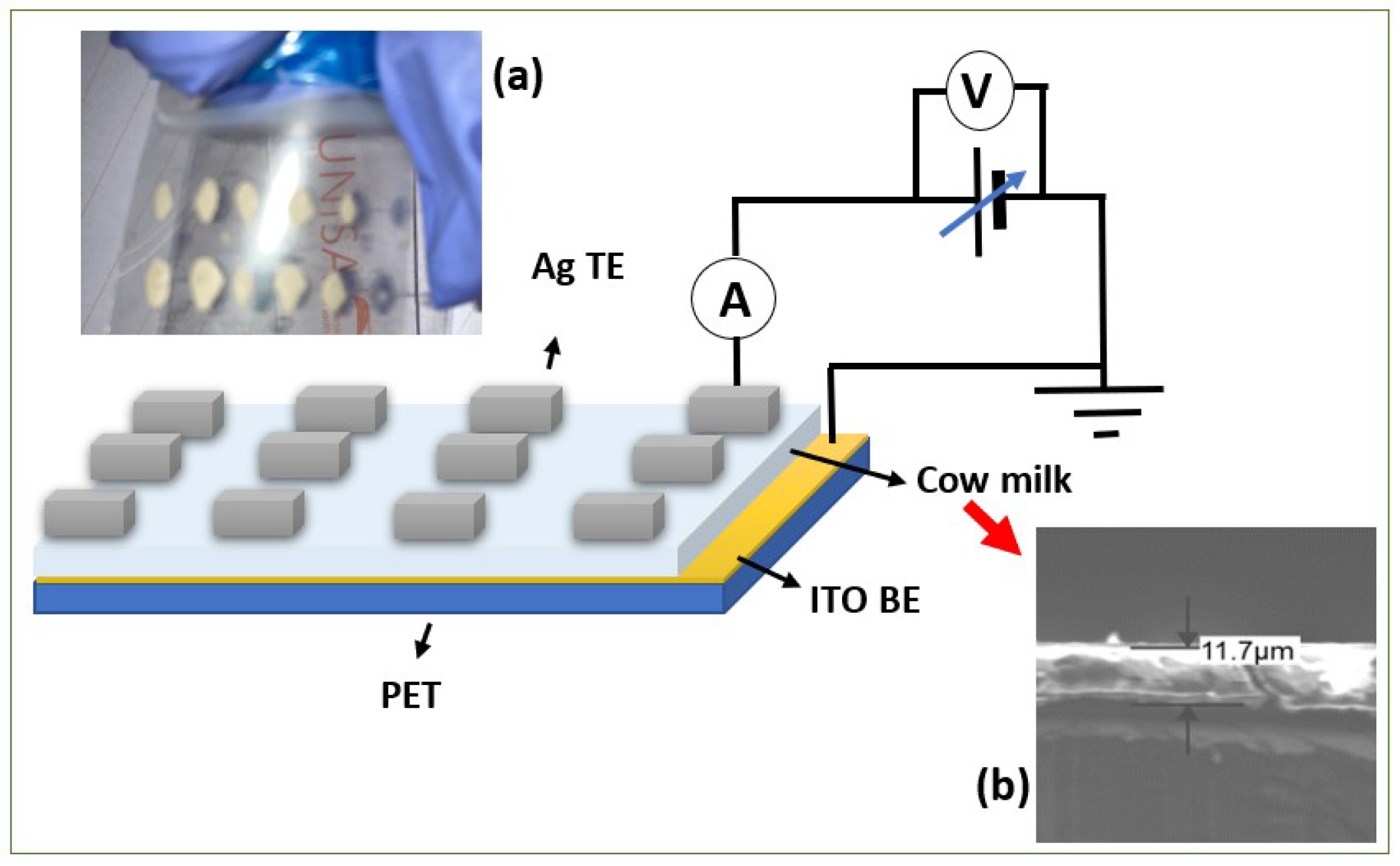
2. Materials and Methods

The organic homogenized cow milk used in this study was purchased from a local supermarket. The direct dipping (or dip-coat) method was used to create our milk films. First, rectangular pieces of polyethylene terephthalate (PET) coated with an indium-doped tin oxide conductive layer (ITO) (from Sigma-Aldrich, St. Louis, MO, USA) were used as substrates as well as the bottom electrodes (BE). The PET-ITO substrates were pre-cleaned for 5 min each with sonication in isopropyl alcohol, ethanol, and ultra-purified water. The substrates were then briefly immersed in fat-free (S1), medium-fat (S2), or full cream (S3) milk. Then, they were gently placed on a horizontal surface with the ITO sides facing up and left to dry at room temperature for 24 h. Then, on top of each milk film, silver paste (Ag) (Sigma-Aldrich, St. Louis, MO, USA) was applied to form electrodes. The devices were then dried at room temperature for 48 h. Three manufactured devices are labeled as follows:
  • PET-ITO/Cow-milk(S1)/Ag
  • PET-ITO/Cow-milk(S2)/Ag, and
  • PET-ITO/Cow-milk(S3)/Ag
The schematic diagram for the manufactured devices is shown in Figure 1, and the actual photograph of one of the devices and the cross-sectional image demonstrating the estimated thickness of 11.7 μ m are shown in Figure 1 insets (a) and (b), respectively.
The following techniques were used for the characterization of the milk film and the entire device. (1) The morphology of the active layers was studied using a field emission gun scanning electron microscope (FEG-SEM) (ZEISS Ultra Plus, Oberkochen, Germany). The thickness of the films was also estimated using this technique. (2) The element composition of the films was estimated using an energy-dispersive X-ray spectrometer (EDS, Oxford Aztoec 350 X-Max80, Concord, MA, USA). (3) The surface properties of the active layers were studied using an atomic force microscope (Nanosurf, FlexAFM, Liestal, Switzerland). Finally, at room temperature, the electric transport and switching study on all devices was carried out using the source/measure unit (SMU) (Keysight, Santa Rosa, CA, USA) series B2901A, which was connected as shown in the simplified circuit diagram in Figure 1 (Main figure).

3. Results

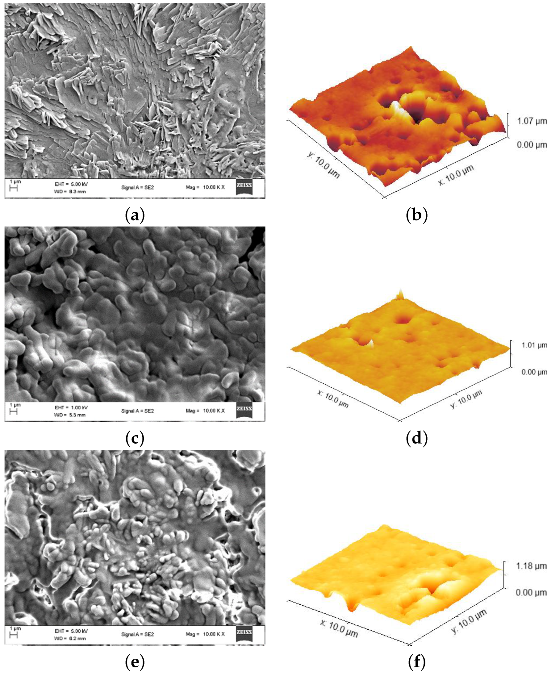
3.1. Morphology and Topography

As shown in Figure 1a, the cow milk-based film was strongly bonded to the ITO surface, forming a stable film even after bending. The element composition of each film was determined using EDS, and the results are shown in Figure 2. Sodium (Na), magnesium (Mg), phosphorus (P), potassium (K), chlorine (Cl), and calcium (Ca) were common elements in all films. There were no traces of contamination in the films, and elements such as carbon (C) and oxygen (O) are thought to occur due to organic compounds in the milk, and the high peak of carbon is due to the carbon coating used during the EDS sample preparation. The nitrogen atom detected is thought to be caused by the protein constituent of milk.
The micrographs presented in Figure 3a,c,e are the FEG-SEM microstructures of cow milk films with varying fat content, namely fat-free, medium fat, and full-cream. The dimensions of the microstructures are 1 μ m × 1 μ m. Based on the observed microstructures, it can be inferred that diminutive fat globules are discernible within the medium cream milk film. Furthermore, these fat globules exhibit greater salience in the micrograph of full cream cow milk. These fat microstructures are missing in fat-free cow milk, leaving only tiny void spaces visible. The AFM topography images for the fat-free, medium-fat, and full-cream milk films are illustrated in Figure 3b,d,f, respectively. The Atomic AFM results indicate notable variations in the surface properties of these films. The fat-free milk based film is characterized by the presence of cavities on all of its surfaces, with a maximum depth of 0.54 μ m. Relatively speaking, the presence of pits is comparatively less conspicuous in the medium cream and full cream milk-based films. The results of the roughness assessment indicate that the mean roughness values for the fat-free, medium fat, and full cream milk-based films were 87.7 nm, 28 nm, and 56 nm, respectively. Compared to other films, fat-free milk is believed to possess a significant proportion of water. During the drying process of the film, the water undergoes evaporation, resulting in the formation of voids that lead to a significant increase in roughness, as evidenced by the AFM findings. The film derived from full cream milk is characterized by a high fat content and low water content. Upon desiccation, the fat component of the film persists and determines its morphology. The optimal amount of water and fat in the medium cream cow milk film is responsible for its comparatively smoother surface.

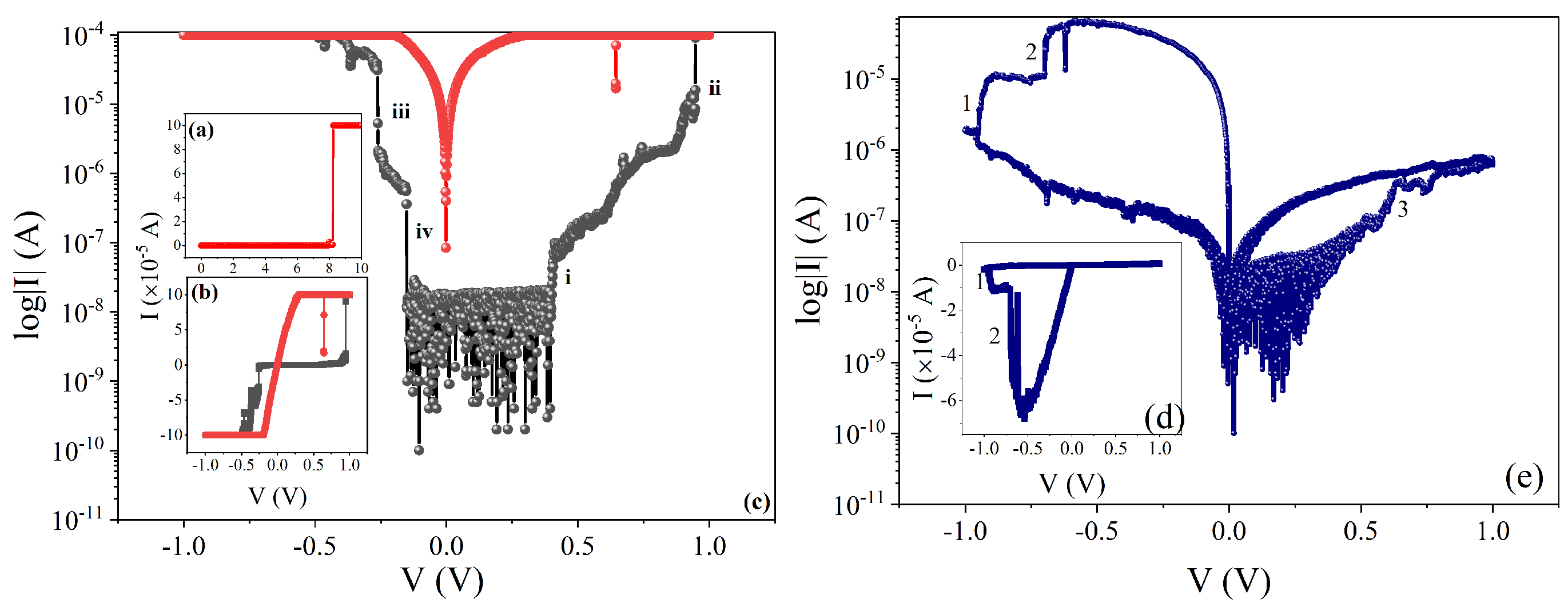
3.2. Transport and Memory Study

An electrical characterization study was conducted at ambient temperature. An applied voltage stress (V) was exerted on the Ag top electrode (TE) while the indium tin oxide (ITO) bottom electrode (BE) was grounded. To initiate the electroforming of each device, a series of single forward scans was performed. The scans consisted of 0 + V m a x voltage steps with a magnitude of 10 mV and a delay time of 2.5 ms. This was necessary because a pristine device is non-conductive. This was performed while measuring the current (I) of the device. A compliance current ( I C C ) of 10 4 A was programmed in order to safeguard the devices against dielectric breakdown. After conducting the electroforming scan, we proceeded to perform full cycle voltage scans ( 0 + V m a x 0 V m a x 0 ) in order to analyze the memory behavior of the devices. This methodology has been previously documented [6,12,13].
Figure 4 depicts the I-V variation of the PET-ITO/cow-milk(S1)/Ag device. For this device, increasing the voltage did not result in an increase in electric current until 8.22 V, when a jump (with ≥10 4 order of magnitude) in current is observed, indicating electroforming (Figure 4a). The I-V (Figure 4b) and l o g | I | V (Figure 4c) graphs depict the memory characteristic hysteresis for this device. Furthermore, these results show clear multilevel switching, namely the SET (write) process at points i and ii, as well as RESET (erase) at points iii and iv, establishing the somewhat asymmetric ‘S-type’ hysteresis with an overall I O N / I O F F 10 [14]. A high I O N / I O F F ratio is advantageous in memory applications because it allows clear readability of the ON (logic 1) and OFF (logic 0) device states. Furthermore, the presence of hysteresis between −1 and +1 V provides a relatively small (≤4 V) memory window for this device. However, the downfall of this device’s behavior was data noise at low (near zero) voltage, as well as a significant change in the I-V variation during the second scan, as depicted in the I-V (Figure 4d) and l o g | I | V (Figure 4e).
Figure 5 depicts the I-V characteristics of the PET-ITO/cow milk(S2)/Ag device. For this device, the current initially follows a linear path before abruptly dropping at 0.59 V . It stayed in the 2 × 10 5 A range for 0.59 0.93 V before abruptly jumping to > 10 4 A as shown in Figure 5a. The event at 0.93 V can be characterized as the electroforming process. The memory characteristics depicted in the I-V (Figure 5b) and log|I|-V (Figure 5c) reveals memory hysteresis with V S E T = + 0.48 V and V R E S E T = 0.25 V . As a result, this is an asymmetric ‘S-type’ bipolar memory behavior [14]. Furthermore, the memory behavior was stable for at least thirty write and read cycles, as shown in Figure 5d. Despite its low (≥10) I O N / I O F F ratio, this device has a lower switching voltage than other organic ReRAM devices, but its endurance of only 30 cycles is a drawback for non-volatile memory applications. Future electronic gadgets, on the other hand, appear to be flexible [15], transparent [15,16], and transient [17]. Yalagala et al. reported on the rapid (<4 s) dissolving of a ReRAM device with a MgO-PVP-Ge active layer and Ag and ITO electrodes [17]. We believe that because our device uses the same electrode materials and milk as the active layer, it will have good transient characteristics. Furthermore, the negligible fabrication costs and low operating voltage of our device make it suitable for short-term use and disposable memory devices.
Finally, Figure 6 depicts the I-V characteristics of the PET-ITO/cow milk(S3)/Ag device. The I-V graph of the electroforming process is shown in Figure 6a. Our data show no forming because the current follows an exponential trajectory and does not increase abruptly. The log|I|-V variation (Figure 6b) illustrating this device’s memory characteristics reveals a typical ‘O-type’ hysteresis [18] lying between 1.70 and + 0.70 V . This ‘O-type’ memory behavior has I O N / I O F F 10 and was sustained for more than 14 write/erase cycles, as shown in Figure 6c,d. As shown in Figure 6d, after the 14th cycle, the device’s resistance began to decrease exponentially, and the HRS and LRS states began to coincide at the 37th cycle. This decrease in the I O N / I O F F ratio indicates that memory behavior is deteriorating.
In comparison, our data show different forming and memory behavior in devices with S1, S2, and S3 active layers. This could be due to the fat content or different weight percentages of the metallic ions in these active layers. The conductive mechanism in each device will be examined in the following subsection.

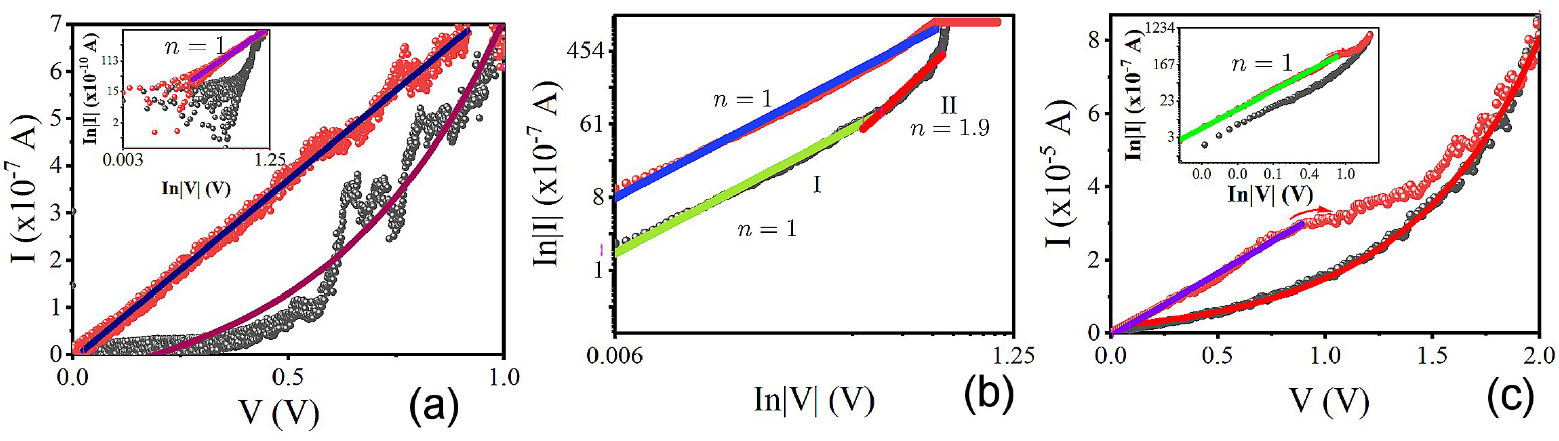
3.3. Conduction Mechanism Analysis

As shown in Figure 7, the I-V data for the PET-ITO/cow-milk(S1)/Ag device have been fitted (a). The OFF and ON state current curves fit the exponential and linear ( s l o p e = 8.0 × 10 7 Ω 1 ) functions very well, respectively. The data were re-plotted on the log-log scale to obtain the exact relationship of current density (J) and V in the linear state, as shown in the inset. The value of n for the relationship J V n was estimated to be 1 based on the slope of the l n I l n V graph (inset). This means that in the ON state, the current follows Ohm’s law ( J V ) given in Equation (1) [19]:
J = q μ n 0 V d
where q is the electronic charge, μ is the mobility, n 0 is the density of the mobile charge carriers and d is the thickness of the sample. Ohmic conduction, in this case, indicates that nanoscale conductive filaments (CFs) are formed in the sample as a result of the electric field application [20]. The current in the OFF state exhibits exponential behavior, indicating the hopping conduction mechanism given in Equation (2) as described in Ref. [18]:
I = I 0 + A exp [ ( V V a ) / k T ]
Here, I 0 is the residual current and A = q a n ν (a, n, and ν are, respectively, the mean hopping distance, the electronic concentration in the dielectric conduction band, and the frequency of thermal vibration at the trap sites; V a is the characteristic voltage relating to the activation energy, k is the Boltzmann constant and lastly, T is the temperature in Kelvin [18].
The conduction mechanism of the PET-ITO/cow-milk(S2)/Ag device is distinct. Figure 7b depicts the l n I l n V graph for this device. The current in the ON and OFF states fit well with the linear function, with n = 1 indicating the presence of CFs. However, the OFF-state current shows two distinct regions with n = 1 (region I) and then n = 1.9 2 (region II), indicating the space charge-limited conduction mechanism (SCLCM) [21,22]. The current in region II follows the Mott–Guyner equation (Equation (3)):
J = 9 μ ε θ V 2 8 D 3
where μ is the mobility, ε is the permittivity of the active layer, θ is the ratio of the free and trapped charge, and d is the thickness of the active layer [23].
Finally, we investigate the PET-ITO/cow-milk(S3)/Ag device’s conduction mechanism. This device’s I-V data fit is depicted in Figure 7c. Again, our data point to hopping conduction-driven CF formation. This is demonstrated by the exponential I-V relationship of the OFF-state current (Figure 7c (main)) and the linear relationship in the ON-state (Figure 7c (inset)).
Based on our research, it has been observed that the cream-based medium device exhibits distinct behavior in comparison to the fat-free and full-cream-based devices. We conducted a comparative analysis of the elemental composition of the three active layers, as presented in Table 1, in an effort to gain a deeper understanding of the matter. The data presented in Table 1 indicates that the S2 device exhibits the greatest weight percentage (wt.%) of Na, Cl, K, Ca, and Cu in comparison to both the S1 and S3 devices. Notably, the S1 device is deficient in certain elements, namely K and Cu. This phenomenon may have contributed to the observed behavioral aberration as indicated by our findings. The results of our investigation do not indicate the precise elements or ions accountable for the creation of CF in our devices. The presence of multiple ions within biological materials poses a challenge due to their potential impact on electronic properties, including electrical transport and switching behaviors. This is a subject that requires further investigation. It is of scientific merit to explore the function of C u 2 + cations in the reported devices. The C u 2 + ions have piqued scientific interest due to two distinct factors. Firstly, these ions are notably absent in the fat-free film, which exhibited suboptimal performance. Conversely, they are more abundant in the medium cream-based films as compared to the full cream-based films. Secondly, from an electrochemical standpoint, the C u 2 + ions exhibit a higher reduction potential in comparison to the other ions present in these films. The mechanism analysis results suggest a potential correlation between the formation of conductive filaments and C u 2 + ions. The application of a voltage across the device results in the production of charges with opposing polarities in the two electrodes. The electrons situated in the negative electrode exhibit a desire to permeate the film, however, they are impeded by the Schottky barrier that exists at the interface between the electrode and the film. The Schottky barrier possesses a barrier height denoted by the symbol Φ . As the voltage is augmented, the barrier height diminishes, thereby enabling the ingress of electrons into the film. The electrons present in the film exhibit interaction with C u 2 + ions and undergo absorption through a reduction reaction ( C u 2 + + 2 e C u ), leading to the creation of a Cu-atom. The subsequent electron has the ability to transition from the electrode to the conductive copper atom and undergo a “hopping” process into the adjacent C u 2 + ion. This sequence of events repeats until all C u 2 + ions in the arrangement have been transformed into copper atoms. This is the current scientific understanding of the mechanism behind hopping conduction. The copper atoms exhibit alignment along the direction of the electric field, resulting in a configuration that bears resemblance to the CF. The observed exponential line shape of the fat-free device is likely attributed to the involvement of ions other than C u 2 + in the conductive sites. The low concentration of these ions, as indicated by the EDS findings, leads to a significant increase in the hopping distance (a) between successive conductive sites. Consequently, more energy is required to overcome this distance. The linear behavior exhibited by the Medium-fat-based film may be ascribed to the high concentration of C u 2 + ions, which results in their close proximity. Due to the application of voltage, the ions undergo a slight drift and subsequently come into contact with the electrode and with each other. This leads to the formation of a more metallic CF following the reduction process. Despite our utmost endeavor, the existence of diverse ions (anionic or cationic), proteins, and organic molecules in milk cannot be entirely disregarded. This will require a comprehensive investigation.
In the end, we compared our findings to those that had been reported previously in the scientific literature; we offer (Table 2) a summary of the memory device parameters that were produced by using some of the raw biological components. Our Ag/cow milk(S2)/ITO device has the lowest ( 0.25 V) switching voltage, surpassing the 0.6 V of the lactose, which also employs Ag and ITO electrodes [9], and is getting close to the 0.1 V record set by the C H 3 N H 3 P b I 3 organic ReRAM [24]. We believe that the metallic ions that were already present in the milk film are responsible for the low operating voltage. The very same table reveals another important fact, namely that the raw bio-ReRAM devices in question utilize SCLCM as their primary switching mechanism.
Finally, we compared our findings to previously reported results in the literature; we present (Table 2) a summary of the memory device parameters achieved using some of the raw biological materials. Our Ag/cow milk(S2)/ITO device has the lowest ( 0.25 V ) switching voltage, surpassing the 0.6 V of the lactose, which also uses Ag and ITO electrodes [9], and approaching the ∼ 0.1 V record set by the C H 3 N H 3 P b I 3 organic ReRAM [24]. We attribute the low operating voltage to the metallic ions already present in the milk film. We can also see from the same table that the switching mechanism in these raw bio-ReRAM devices is primarily SCLCM.

4. Conclusions

Resistive switching memory devices were fabricated utilizing active layers of raw organic cow milk with varying fat content, including fat-free, medium-cream, and full-cream. The phenomenon of switching was detected in the medium cream milk-based apparatus at a minimal voltage of 0.25 V, thereby enabling its operation as a memory device with low power consumption. Devices with low power consumption are of utmost importance for the development of environmentally sustainable technology and electronics. The fat and metal element composition of cow milk has an impact on its physical structure, electrical transport, and resistive switching. The device utilizing medium-fat cow milk exhibited superior morphology and memory behavior compared to those utilizing fat-free and full-cream milk. The electric transport mechanism observed in both fat-free and full cream devices has been ascribed to conducting filaments driven by hopping conduction. The operational principle of the device based on medium-fat cow milk was ascribed to conductive filaments driven by space-charge limited conduction mechanism. The results of our study indicate that the functionality of the ReRAM device based on cow milk is significantly dependent on the inherent metallic ions present in milk. Consequently, the dispersion of conductive nanoparticles within milk can be utilized to customize its suitability in ReRAM technology, thereby facilitating additional optimization.

Author Contributions

Conceptualization, Z.W.D., S.V. and V.S.V.; Formal analysis, Z.W.D.; Investigation, Z.W.D. and S.V.; Methodology, Z.W.D., S.V. and V.S.V.; Supervision, V.S.V.; Writing—original draft, Z.W.D.; Writing—review & editing, Z.W.D. All authors have read and agreed to the published version of the manuscript.

Funding

This research was funded by National Research Foundation ZA grant number 134133.

Data Availability Statement

The data used in this study is available from the corresponding author upon reasonable request.

Acknowledgments

Zolile likes to acknowledge NRF-ZA for the financial support, and the South African Department of Higher education and training for granting me the Next Generation of Academics Program (nGAP) opportunity at CUT.

Conflicts of Interest

The authors declare no conflict of interest. The funders had no role in the design of the study; in the collection, analyses, or interpretation of data; in the writing of the manuscript; or in the decision to publish the results.

Abbreviations

The following abbreviations are used in this manuscript:
ReRAMResistive Switching Memory
TETop electrode
BEBottom electrode
SCLCMSpace charge-limited conduction mechanism
CBCMConductive bridge conduction mechanism

References

  1. Hickmott, T.W. Low-Frequency Negative Resistance in Thin Anodic Oxide Films. J. Appl. Phys. 1962, 33, 2669–2682. [Google Scholar] [CrossRef]
  2. Tseng, R.J.; Tsai, C.; Ma, L.; Ouyang, J.; Ozkan, C.S.; Yang, Y. Digital memory device based on tobacco mosaic virus conjugated with nanoparticles. Nat. Nanotechnol. 2006, 1, 72–77. [Google Scholar] [CrossRef] [PubMed]
  3. Li, Y.Y.; Qian, Q.; Zhu, X.; Li, Y.Y.; Zhang, M.; Li, J.; Ma, C.; Li, H.; Lu, J.; Zhang, Q. Recent advances in organic-based materials for resistive memory applications. InfoMat 2020, 2, 995–1033. [Google Scholar] [CrossRef]
  4. Jeong, D.S.; Thomas, R.; Katiyar, R.S.; Scott, J.F.; Kohlstedt, H.; Petraru, A.; Hwang, C.S. Emerging memories: Resistive switching mechanisms and current status. Rep. Prog. Phys. 2012, 75, 076502. [Google Scholar] [CrossRef]
  5. Vallabhapurapu, S.; Sangani, L.D.V.; Krishna, M.G.; Das, J.; Srinivasan, A.; Srinivasu, V.V. Optical and resistive switching properties of Chitosan-aluminum-doped zinc oxide composite thin films for transparent resistive random access memory application. J. Mater. Sci. Mater. Electron. 2021, 32, 3556–3565. [Google Scholar] [CrossRef]
  6. Dlamini, Z.W.; Vallabhapurapu, S.; Wu, S.; Mahule, T.S.; Srivivasan, A.; Vallabhapurapu, V.S. Resistive switching memory based on chitosan/polyvinylpyrrolidone blend as active layers. Solid State Commun. 2022, 345, 114677. [Google Scholar] [CrossRef]
  7. Hwang, S.W.; Song, J.K.; Huang, X.; Cheng, H.; Kang, S.K.; Kim, B.H.; Kim, J.H.; Yu, S.; Huang, Y.; Rogers, J.A. High-Performance Biodegradable/Transient Electronics on Biodegradable Polymers. Adv. Mater. 2014, 26, 3905–3911. [Google Scholar] [CrossRef]
  8. Hosseini, N.R.; Lee, J.S.S. Biocompatible and Flexible Chitosan-Based Resistive Switching Memory with Magnesium Electrodes. Adv. Funct. Mater. 2015, 25, 5586–5592. [Google Scholar] [CrossRef]
  9. Guo, Y.; Hu, W.; Zeng, F.; Zhang, C.; Peng, Y.; Guo, Y. Ultrafast degradable resistive switching memory based on α-lactose thin films. Org. Electron. 2020, 83, 105750. [Google Scholar] [CrossRef]
  10. Lv, F.; Ling, K.; Zhong, T.; Liu, F.; Liang, X.; Zhu, C.; Liu, J.; Kong, W. Multilevel Resistive Switching Memory Based on a CH3NH3PbI 3-xClx Film with Potassium Chloride Additives. Nanoscale Res. Lett. 2020, 15, 126. [Google Scholar] [CrossRef]
  11. Dlamini, Z.W.; Vallabhapurapu, S.; Mahule, T.S.; Vallabhapurapu, V.S. Electrical conduction and resistive switching in cow milk-based devices prepared using the spin-coat method. AIP Adv. 2022, 12, 095321. [Google Scholar] [CrossRef]
  12. Dlamini, Z.W.; Vallabhapurapu, S.; Daramola, O.A.; Tseki, P.F.; Krause, R.W.M.; Siwe-Noundou, X.; Mahule, T.S.; Vallabhapurapu, S.V. Conduction and Resistive Switching in Dropcast CdTe/CdSe Core-Shell Quantum Dots Embedded Chitosan Composite. Iran. J. Sci. Technol. Trans. A Sci. 2022, 46, 709–716. [Google Scholar] [CrossRef]
  13. Dlamini, Z.; Vallabhapurapu, S.; Srinivasan, A.; Wu, S.; Vallabhapurapu, V. Resistive Switching in Polyvinylpyrrolidone/Molybdenum Disulfide Composite-Based Memory Devices. Acta Phys. Pol. A 2022, 141, 439–444. [Google Scholar] [CrossRef]
  14. Prime, D.; Paul, S. Overview of organic memory devices. Philos. Trans. R. Soc. A Math. Phys. Eng. Sci. 2009, 367, 4141–4157. [Google Scholar] [CrossRef]
  15. Park, J.; Huh, D.; Son, S.; Kim, W.; Ju, S.; Lee, H. Transparent, Flexible, and Low-Operating-Voltage Resistive Switching Memory Based on Al2Ol3/IZO Multilayer. Glob. Challenges 2022, 6, 2100118. [Google Scholar] [CrossRef]
  16. Kim, J.; Park, J.; Kim, S. Bipolar Switching Characteristics of Transparent WOX-Based RRAM for Synaptic Application and Neuromorphic Engineering. Materials 2022, 15, 7185. [Google Scholar] [CrossRef]
  17. Yalagala, B.; Khandelwal, S.; Deepika, J.; Badhulika, S. Wirelessly destructible MgO-PVP-Graphene composite based flexible transient memristor for security applications. Mater. Sci. Semicond. Process. 2019, 104, 104673. [Google Scholar] [CrossRef]
  18. Vallabhapurapu, S.; Rohom, A.; Chaure, N.B.; Tu, C.; Du, S.; Srinivasu, V.V.; Srinivasan, A. Hopping conductivity-mediated O-shaped memory behaviour in gelatin–graphene oxide composite films. Appl. Phys. A 2018, 124, 1–5. [Google Scholar] [CrossRef]
  19. Shen, Z.; Zhao, C.; Qi, Y.; Xu, W.; Liu, Y.; Mitrovic, I.Z.; Yang, L.; Zhao, C. Advances of RRAM devices: Resistive switching mechanisms, materials and bionic synaptic application. Nanomaterials 2020, 10, 1437. [Google Scholar] [CrossRef]
  20. Yu, S. Resistive Random Access Memory (RRAM). Synth. Lect. Emerg. Eng. Technol. 2016, 2, 1–79. [Google Scholar]
  21. Dlamini, Z.W.; Vallabhapurapu, S.; Daramola, O.A.; Tseki, P.F.; Krause, R.W.M.; Siwe-Noundou, X.; Mahule, T.S.; Vallabhapurapu, S.V. Resistive Switching in CdTe/CdSe Core–Shell Quantum Dots Embedded Chitosan-Based Memory Devices. J. Circuits Syst. Comput. 2022, 31, 1–16. [Google Scholar] [CrossRef]
  22. Sun, T.; Tu, J.; Zhou, Z.; Sun, R.; Zhang, X.; Li, H.; Xu, Z.; Peng, Y.; Liu, X.; Wangyang, P.; et al. Resistive switching of self-assembly stacked h-BN polycrystal film. Cell Rep. Phys. Sci. 2022, 3, 100939. [Google Scholar] [CrossRef]
  23. Lim, E.W.; Ismail, R. Conduction mechanism of valence change resistive switching memory: A survey. Electronics 2015, 4, 586–613. [Google Scholar] [CrossRef]
  24. Choi, J.; Park, S.; Lee, J.; Hong, K.; Kim, D.H.; Moon, C.W.; Park, G.D.; Suh, J.; Hwang, J.; Kim, S.Y.; et al. Organolead Halide Perovskites for Low Operating Voltage Multilevel Resistive Switching. Adv. Mater. 2016, 28, 6562–6567. [Google Scholar] [CrossRef]
  25. Zhou, G.; Yao, Y.; Lu, Z.; Yang, X.; Han, J.; Wang, G.; Rao, X.; Li, P.; Liu, Q.; Song, Q. Hydrogen-peroxide-modified egg albumen for transparent and flexible resistive switching memory. Nanotechnology 2017, 28, 425202. [Google Scholar] [CrossRef] [PubMed]
  26. Zhou, G.; Sun, B.; Zhou, A.; Wu, B.; Huang, H. A larger nonvolatile bipolar resistive switching memory behaviour fabricated using eggshells. Curr. Appl. Phys. 2017, 17, 235–239. [Google Scholar] [CrossRef]
  27. Qin, S.; Dong, R.; Yan, X.; Du, Q. A reproducible write-(read)n-erase and multilevel bio-memristor based on DNA molecule. Org. Electron. 2015, 22, 147–153. [Google Scholar] [CrossRef]
  28. Liu, S.; Dong, S.; Wang, X.; Shi, L.; Xu, H.; Huang, S.; Luo, J. Flexible and fully biodegradable resistance random access memory based on a gelatin dielectric. Nanotechnology 2020, 31, 255204. [Google Scholar] [CrossRef]
  29. Wang, H.; Zhu, B.; Wang, H.; Ma, X.; Hao, Y.; Chen, X. Ultra-Lightweight Resistive Switching Memory Devices Based on Silk Fibroin. Small 2016, 12, 3360–3365. [Google Scholar] [CrossRef]
  30. Raeis-Hosseini, N.; Lee, J.S. Controlling the Resistive Switching Behavior in Starch-Based Flexible Biomemristors. ACS Appl. Mater. Interfaces 2016, 8, 7326–7332. [Google Scholar] [CrossRef]
  31. Sun, B.; Zhu, S.; Mao, S.; Zheng, P.; Xia, Y.; Yang, F.; Lei, M.; Zhao, Y. From dead leaves to sustainable organic resistive switching memory. J. Colloid Interface Sci. 2018, 513, 774–778. [Google Scholar] [CrossRef] [PubMed]
  32. Qi, Y.; Sun, B.; Fu, G.; Li, T.; Zhu, S.; Zheng, L.; Mao, S.; Kan, X.; Lei, M.; Chen, Y. A nonvolatile organic resistive switching memory based on lotus leaves. Chem. Phys. 2019, 516, 168–174. [Google Scholar] [CrossRef]
  33. Lim, Z.X.; Sreenivasan, S.; Wong, Y.H.; Zhao, F.; Cheong, K.Y. Filamentary Conduction in Aloe Vera Film for Memory Application. Procedia Eng. 2017, 184, 655–662. [Google Scholar] [CrossRef]
Figure 1. The main diagram depicts a typical PET-ITO/cow milk/Ag ReRAM device connected to a simplified current-voltage measurement circuit. The insets show (a) the actual PET-ITO/Cow milk(S2)/Ag ReRAM photograph and (b) a cross-sectional FESEM micrograph of the S2 active layer.
Sustainability 15 08250 g001
Figure 2. EDS spectrum of cow milk.
Sustainability 15 08250 g002
Figure 3. This figure shows FEG-SEM micrographs of (a) fat-free (S1), (c) medium cream (S2), and (e) full-cream (S3) cow milk films. On the same image, (b,d,f) show the AFM topography images of the fat-free, medium cream and full cream cow milk, respectively.
Sustainability 15 08250 g003
Figure 4. I-V characteristics of the PET-ITO/cow milk(S1)/Ag device, showing (a) the forming curve, the first full cycle voltage scan data in (b) linear and (c) semi-log scale (The black and red curves represent the forward and reverse voltage sweep, respectively). On the same figure, (d,e) are linear scale and semi-log graphs for the second full cycle voltage scan.
Sustainability 15 08250 g004
Figure 5. I-V characteristics of the PET-ITO/cow milk(S2)/Ag device, showing (a) the forming curve, the first cycle scan in I-V (b) and log|I|-V (c), as well as (d) the log|I|-V graphs for the first 30 sweeping cycles.
Sustainability 15 08250 g005
Figure 6. I-V characteristics of the PET-ITO/cow milk(S3)/Ag device, showing (a) the forming curve, (b) the first, and (c) the first 80 sweeping cycles. (d) on the other hand, shows the resistance-number of sweeping cycle.
Sustainability 15 08250 g006
Figure 7. (a) The I-V (main figure) and ln|I|-ln|V| (inset) curve fitting of the PET-ITO/cow milk(S1)/Ag device. (b) The ln|I|-ln|V| curve fitting of the PET-ITO/cow milk(S2)/Ag device. (c) The I-V (main figure) and ln|I|-ln|V| (inset) curve fitting of the PET-ITO/cow milk(S3)/Ag device.
Sustainability 15 08250 g007
Table 1. The comparative summary of metallic element content ( wt . % ) from the EDS data, switching type, and conduction mechanism of fat-free, medium fat, and full ream raw cow milk-based active layers.
Active Layer Estimated Element Content ( wt . % )Switching TypeConduction Mechanism
NaClKCaCu
Fat-free0.440.51-0.67-‘O-type’Hopping conduction
Medium cream2.374.727.425.071.08‘S-type’SCLC
Full-cream0.310.881.130.910.42‘O-type’Hopping conduction
Table 2. A synopsis of organic-ReRAMs, their memory parameters, and switching mechanisms.
DeviceOperating Voltage I ON / I OFF RatioRetention (s)Endurance (Cycles)Conduction MechanismRef.
Ag/cow milk(S2)/ITO0.25∼10no report>30SCLCMThis work
Ag/ α -lactose/ITO0.6No report5000100SCLCM[9]
Mg/albumen/W1 10 2 10 3 10 2 SCLCM[25]
Ag/eggshell/FTO1.12 10 3 10 3 100SCLCM[26]
Au/DNA/Au0.73∼10 10 6 10 2 SCLCM[27]
Mg/gelatin/W2.16 10 2 10 4 10 2 SCLCM[28]
Ag/fibroin/Au0.7 10 5 10 4 30SCLCM[29]
Au/starch/ITO0.9 10 3 10 4 No reportSCLCM[30]
Ag/Banyan leaves/Ti150 10 3 No reportSCLCM[31]
Ag/Lotus leaves/ITO340 10 3 >70CBCM 1[32]
Ag/Aloe Vera/ITO0.75 10 4 > 10 4 10 2 CBCM[33]
1 CBCM stands for conductive bridge conduction mechanism.
Disclaimer/Publisher’s Note: The statements, opinions and data contained in all publications are solely those of the individual author(s) and contributor(s) and not of MDPI and/or the editor(s). MDPI and/or the editor(s) disclaim responsibility for any injury to people or property resulting from any ideas, methods, instructions or products referred to in the content.

