Abstract
Multilevel inverters (MLIs) have recently attracted more attention in medium-voltage and high-power applications as they can provide an effective interface with photovoltaic (PV) systems. Conventional MLIs are used to generate higher voltage levels, which improve power quality and reduce the requirement for passive filters. However, recent research has focused on designing new MLI topologies using reduced switch counts and less voltage stress. This study, as such, proposes a new nine-level symmetric MLI for PV systems with a minimum number of switches. This decrease in the number of switches reduces the voltage stress across the switches and the number of driving circuits, which lowers the complexity of the control circuit and, as a result, lowers the cost and size of the system. This article compares the proposed MLI with other topologies based on the DC sources, switches count, gate driver circuits (Ngd), total standing voltage per unit (TSVPU), cost function (CF), and components count per level (CC/L). The proposed topology is integrated with the PV system. MATLAB software is used to evaluate the performance of MLI at step change in irradiance and under variable load conditions. The total harmonic distortion (THD) of the proposed topology is reduced with the implementation of phase disposition pulse width modulation (PD-PWM). In addition, PD-PWM is compared with phase opposition disposition pulse width modulation (POD-PWM) and alternative phase opposition disposition pulse width (APOD-PWM) modulation techniques. The simulation results reveal the improved performance of the proposed topology at variable irradiance and under varying load conditions. The comparison results reveal minimum (TSVPU), CC/L, CF, and switch count compared to existing topologies. Hence, the proposed topology of MLI is cost-effective and superior in all aspects compared to other topologies. In summary, it offers overall improved performance, and thus, it is feasible for the PV system.
1. Introduction
Due to the high cost and scarcity of fossil fuels, as well as the necessity to minimize greenhouse gas emissions, renewable resources are becoming more desirable in the field of research [1]. PV is a commonly used renewable energy source. PV energy has many advantages, such as a pollution-free energy resource with a low operating cost, low maintenance cost, and longer life [2]. Inverter is the main component of the PV system that converts DC power to AC, as required by the load [3]. Previously, 2-level inverters were used in a PV, but these are less efficient devices and generate more losses in the system [4].
Furthermore, two-level inverters are limited to low-voltage sectors [5]. In high-power and medium-voltage applications, MLI topologies are employed instead of two-level inverters [6]. The ability of MLIs to meet the demand for power quality and rating has led to their deployment in power systems [7]. MLIs have numerous advantages over 2-level inverters, such as high modularity, smaller common-mode voltage, and reduced electromagnetic compatibility [8]. However, with the increase in voltage levels, more switches are required in this topology, thus increasing the number of components, , and the cost of the system [9]. Therefore, great attention has been given to the new topologies of an MLI having a reduced device count structure with minimum switches, minimum and low CF [10].
Many topologies of MLIs have been discussed in this article. The topology in [11] examined the new topology of MLI, which has 11 switches for the nine-level inverter. This topology has high , high CF, and more CC/L. The author in [12] presents a symmetric MLI. It consists of 10 switches for the nine-level inverter, but the , CF, and CC/L are high. In [13], the author proposed a nine-level symmetric MLI, which uses 12 switches to enhance the voltage levels. In [14], the modified topology of the MLI is proposed. A nine-level MLI requires 11 switches for the nine-level inverter in this topology. In [15], a modified topology of MLI is presented. In this topology, a nine-level inverter requires 12 switches. In [16], a new nine-level cascaded MLI is designed, which consists of 12 switches. In [17],12 switches are required to design a modified nine-level symmetric MLI. In [18], the author presents a modified MLI topology. This topology consists of 12 switches for a nine-level output. In [19], a new single-phase cascaded MLI is designed. In this work, 11 switches are required to design a nine-level inverter. In [20], the author proposed a new topology of the nine-level symmetrical MLI. This topology needs 12 switches for the nine-level MLI. In this proposed work [21], a new topology of nine-level MLI of reduced devices is designed. This topology of nine-level MLI uses 14 switches. This topology has the disadvantage that it can withstand faults at least seven levels. In [22], the author studied an asymmetric UXE-single-source MLI. This topology proposed a nine-level inverter. This topology uses twelve switches for the nine-level inverter. In [23], a UXE-type inverter is proposed. This topology uses twelve switches for the MLI. This topology requires more switches with the increase in voltage levels. The author in [24], proposed a dependable five-level inverter topology. In this topology, nine switches are used for the five-level inverter. The drawback of this topology is that more switches are required with the voltage levels. In [25], the proposed MLI’s basic circuit produces eleven output voltage levels. This topology consists of 11 switches for nine-level inverters. The drawback of this topology is that more switches are required with the increase in voltage levels. In [26], the author proposed a nine-level inverter for a PV system which requires 12 switches.
In light of this, a new topology of MLI based on a reduced switch count, reduced components, low total standing voltage, and minimum system cost is proposed. The proposed topology consists of ten switches and four DC sources. Several parameters of the proposed topology, such as CC/L, , and CF, have been calculated to analyze the performance of the new topology of MLI. The proposed topology is compared with other existing topologies regarding DC sources, switches, diodes, capacitors, gate driver circuits, , CF, and CC/L. In this article, the proposed topology is integrated with the PV system. In this system, the PV arrays are connected to the proposed MLI’s input using DC-DC boost converters, and the PV array voltages are controlled using PI controllers. The performance of the new topology of MLI with has been analyzed at a step change in PV irradiance and is tested under different loads.
Furthermore, the modulation method is another crucial element of an inverter, closely related to THD. The commonly used PWM techniques are PD-PWM, POD-PWM and APOD multicarrier PWM techniques. Using PD-PWM, the carrier signals above and below zero have the same magnitude and phase angle. The carrier signals in the POD-PWM technique are 180 phases shifted between those above and below the reference voltage. The alternate carrier signals are 180 phases shifted in APOD-PWM. These produce low switching losses and low harmonic distortion [27]. In this research work, the PD-PWM technique is designed to reduce the harmonics in the output waveform of the new topology of MLI. This technique is also compared with the POD-PWM and APOD-PWM techniques.
This paper is prepared as the proposed topology of the new symmetric MLI is described in Section 2. This section describes the generalized arrangement, design equations, switching states, and modes of operation of the new topology of the MLI. This section proposed the complete diagram of the proposed topology and the diagram of the DC-DC boost converter with PV system with PI controllers. The control circuit of the new topology of MLI is described in Section 3. A comparative analysis of the proposed topology with existing topologies of the MLI is described in Section 4. Section 5 presents the simulation results of the proposed topology. Section 6 interprets the simulation results. Section 7 summarizes the paper.
2. Materials and Methods
2.1. Proposed New Multilevel Inverter Topology
Figure 1 shows the new topology of symmetric nine-level MLI. For simplification, the PV stages are replaced with DC sources. It consists of 10 switches and 4 DC sources. Symmetric MLI consists of an equal magnitude of voltage sources. The magnitude of the four voltage sources is selected in the ratio of 1:1:1:1 with voltage magnitude of 24 V.
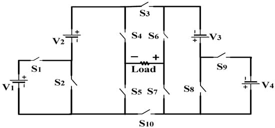
Figure 1.
New topology of the nine-level symmetric multilevel inverter.
The overall voltage magnitude of a symmetric MLI is given in Equation (1):
Or .
In symmetrical MLI, all voltage sources are equal in magnitude. Thus,
The number of effective output voltage levels is given in Equation (2):
where n is the number of voltage sources in each leg. In this topology, two sources are connected in each leg. Therefore, nine levels of output voltage are generated.
nlevel = 4n + 1
In the proposed MLI, several DC voltage sources, no. of switches, and no. of gate driver circuits can be found using Equations (3)–(5).
2.1.1. Switching States of New Multilevel Inverter
The switching states of the proposed nine-level MLI are presented in Table 1. This topology generates nine voltage levels which consist of 0, ±1, ±2, ±3, ±4. This switching scheme generates four positive voltage steps from +V to +4V, zero output voltage steps, and four negative voltage steps from −V to −4V.

Table 1.
Switching states of 9-Level Symmetric New MLI.
2.1.2. Modes of Operation of Proposed Topology
Figure 2 shows the operating modes of the new topology of MLI. To produce + mode 1 activates switches are shown in Figure 2a. Mode 2 activates switches to produce +2 are shown in Figure 2b. Figure 2c shows that mode three is activated to produce by turning on . Mode 4 activates switches to generate are shown in Figure 2d. Mode 5 is activated by turning on switches but cannot generate output voltage as shown in Figure 2e. In this manner, modes 6, 7, 8, and 9 generate negative polarity outputs according to the same operation phase as Modes 1 to 5, shown in Figure 2f–i.
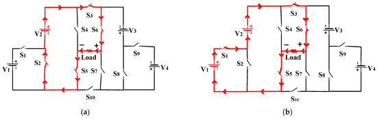
Figure 2.
Active stages of voltage generation level for different modes (a) + (b) +2 (c) +3 (d) +4 (e) 0 (f) (g) (h) (i) .
2.2. Total Standing Voltage (TSV)
In MLI, the TSV of the switch is one of the significant parameters determining the MLI’s cost-effectiveness. The cost of the inverter decreases with the decrease in stress across the semiconductor switches. Standing voltage is the highest voltage stress a power device can withstand while turning off. The sum of all maximum blocking voltages across the switches is the TSV [28]. The maximum blocking voltage (MBV) across each switch is given as follows:
The formula of total standing voltage is given in Equations (6) and (7):
TSV per unit can be calculated by using Equation (8):
where, is the total standing voltage, and is the maximum output voltage.
For the proposed nine-level MLI, is calculated as:
2.3. Cost Function (CF)
Another important parameter of MLI is the cost function (CF). The CF is crucial for selecting the MLI that is most appropriate for the application.CF can be calculated by considering the switches count , DC sources count , capacitors , , diodes count , and gate drivers count [29]. The cost function is given in Equation (9):
where, is the cost coefficient.
The is 0.5 (<1) and 1.5 (>1) for the usual operating state. For the nine-level MLI, the CF/level is calculated as:
For, the cost function is given as
For α = 1.5, the cost function per level is given as
2.4. Components Count per Level (CC/L)
Components count per level is a method used to calculate the number of components per level. The MLI needs more components for the desired voltage levels if the CC/L is high. Thus, the factor needs to be decreased. The CC/L is computed by using Equation (10) [30].
For the proposed nine-level MLI, is calculated as:
2.5. Boost Converter with PV System with PI Controller
The PV Panel is coupled with a DC/DC converter with PI controllers to enhance the performance of the PV system and obtain consistent output voltage at varying irradiance. Implementing PI controllers is the main advantage of irradiance change in the DC-DC converter. Therefore, this work uses a DC-DC boost converter with a PI controller to provide the optimum voltage for the proposed [31]. Figure 3 shows the complete proposed system for the new topology of a nine-level inverter with ten switches and four PV panels. Figure 4 shows the PV system, which includes a PV system and a boost converter with PI controllers.
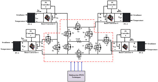
Figure 3.
Complete diagram of the proposed nine-level MLI topology.
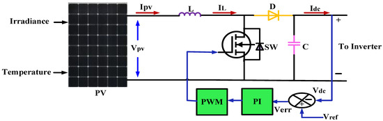
Figure 4.
Boost converter with PV input and PI voltage feedback controller.
The output voltage of the boost converter is given in Equation (11):
here, D is the duty ratio, is the input voltage, and is the output voltage.
The duty ratio is given in Equation (12):
here, is the turn-on time, is the switching time of the semiconductor Switch.
Inductance can be found by using Equation (13):
here, L is the inductance, and is the Switching frequency.
Capacitance can be found by using Equation (14):
here, C is the capacitance, Io is the output current, is a change in voltage i–e (1 to 5% of ).
3. Control Circuit of New Topology of MLI
For the nine-level output, PWM pulse generation is required. It is always necessary to determine which PWM best matches the new topology. Using phase disposition, the THD value of MLIs can be drastically decreased to the lowest possible percentage. By comparing the pulses produced by carrier-shifted signals to a sinusoidal wave, power switches can be turned on [27]. A control circuit for the voltage waveform associated with the carrier signals produced by the PD-PWM approach is shown in Figure 5a. The eight carrier signals required to modulate the reference signal using the PD-PWM approach are shown in Figure 5b. Figure 5c shows the control signals for each switch (.
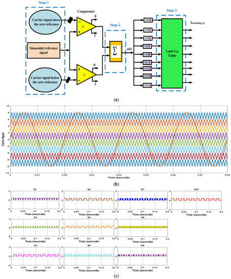
Figure 5.
Phasedisposition PWM for ten switches with nine levels. (a) PDPWM control circuit (b) Carrier signals with the reference signal (c) Control signals for ten-switch () of the proposed nine-level MLI.
The triangular carrier for the m level is given in Equation (15): [32].
Triangular carriers = m − 1
Upper triangular signals are given in Equation (16):
Lower triangular signals are given in Equation (17):
If the upper triangular signal is less than the reference signal, then the comparator generates.
If the lower triangular signal is less than the reference signal, then the comparator generates.
Modulation index ) is given in Equation (18): [33]
where, is the amplitude of the carrier signal, is the amplitude of the modulating signal, and m is the number of levels.
The frequency ratio is given in Equation (19):
where is modulating frequency, and is the carrier frequency.
4. Comparative Analysis
Table 2 compares the proposed topology with conventional and other modified topologies of MLIs based on the number of DC sources, switches, gate diver circuits, diodes, no. of capacitors, , CC/L, and CF. The DC sources in topology [11], the DC sources are 4, but the switches, gate driver circuits, , CF, and components count per level are high. In [12], the DC sources and switches are the same as the proposed topology, but CC/L, , and CF are high compared to the proposed topology. In the other topologies mentioned below, all parameters have been calculated as high except DC sources.
Table 2.
Comparison of proposed topology with other topologies of MLI.
Similarly, Table 3 compares the number of switches concerning the voltage levels, which shows that switches in other existing topologies of MLI are greater than the proposed topology of MLI.
Table 3.
Comparison of proposed topology with other topologies of MLI.
The graphical representation of respective comparisons is shown in Figure 6. Figure 6a compares the total standing voltage per unit ( of the proposed topology compared with other existing topologies. Figure 6b compares the number of gate driver circuits ( of the proposed topology with other existing topologies. Figure 6c shows the number of component counts per level (CC/L) in the proposed topology with other existing topologies. Figure 6d compares the cost function per level (CF/L) at 0.5 and 1.5 values of the cost coefficient of the proposed topology with other existing topologies. The comparison graph between no. of switches concerning voltage levels is shown in Figure 7. It shows that the proposed topology requires fewer switches with an increase in voltage levels compared to existing topologies of MLIs.
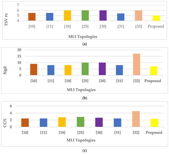
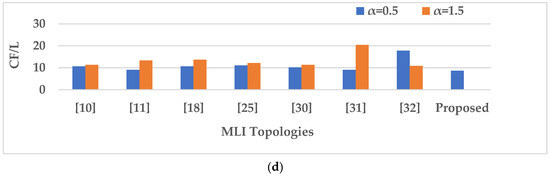
Figure 6.
Comparisons of the new topology of MLI with the existing topologies (a) (b) Ngd (c) CC/L (d) CF/L.
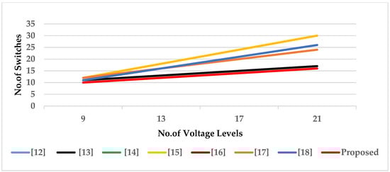
Figure 7.
Line graph between no. of voltage Levels versus no. of switches.
5. Results
The simulation was carried out using MATLAB/Simulink. The applied parameters and their values are given in Table 4. The output PV groups (DC sources) are 24 V, functioned as symmetric sources to verify the nine-level output voltage inverter. Investigations were conducted on a new topology of MLI circuit having a maximum output voltage of approximately 96 V, four DC voltage sources, and ten switches.
Table 4.
Simulation parameters of the proposed system.
In the first case, the resistive load is 12 Ω, and the PV irradiance varies from 1000 to 800 from 0.04 s to 0.14 s as shown in Figure 8a. The variation in PV voltage concerning irradiance is shown in Figure 8b. Figure 8c shows the variation in PV current. Since PI controllers are implemented with four PV arrays with boost converters to maintain the outputs of the proposed topology at variable irradiance. The constant DC voltage is shown in Figure 8d. Each produces a DC constant voltage of 24 V. The constant DC current is shown in Figure 8e. Figure 9 shows the load voltage and load current of the proposed topology nine-level MLI. Figure 10 shows the load current of the proposed topology. Fast Fourier Transform (FFT) spectrum of the load voltage and load current with PD-PWM are shown in Figure 11 and Figure 12.
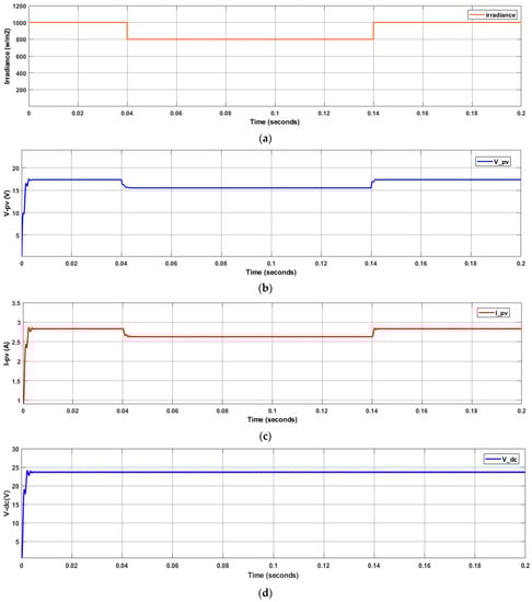
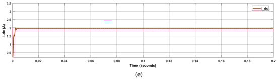
Figure 8.
(a) PV irradiance (b) PV voltage at variable irradiance (c) PV current at variable irradiance (d) DC voltage at variable irradiance (e) DC current at variable irradiance.
Figure 9.
Load voltage and load current of the proposed topology at variable irradiance.
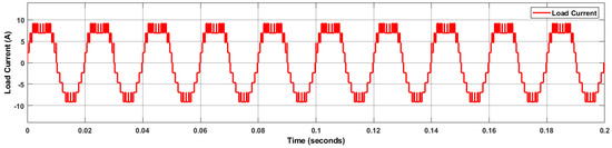
Figure 10.
The load current of the proposed topology at variable irradiance.
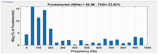
Figure 11.
FFT spectrum of the load voltage with PD-PWM at variable irradiance.
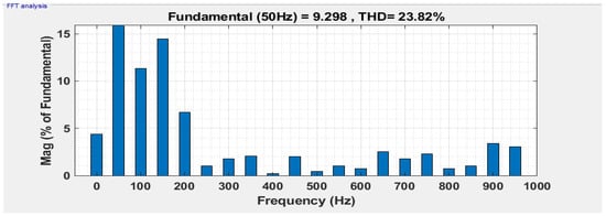
Figure 12.
FFT spectrum of the load current with PD-PWM at variable irradiance.
In the second simulation scenario, resistive-inductive load of R = 12 Ω, L = 1 mH is used to test the topology. Figure 13 displays the load voltage and current waveforms. The load current waveform under a resistive-inductive load behaves differently than a purely resistive load and differs from the voltage waveform. According to the inductor value utilized, the current is smoothed due to inductive load. The load current waveform is shown in Figure 14. FFT analysis of both waveforms is shown in Figure 15 and Figure 16.
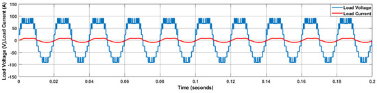
Figure 13.
Load voltage and load current of the proposed topology.
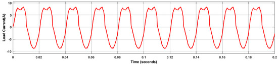
Figure 14.
The load current of the proposed topology.
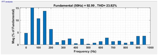
Figure 15.
FFT spectrum of the load voltage with PD-PWM.
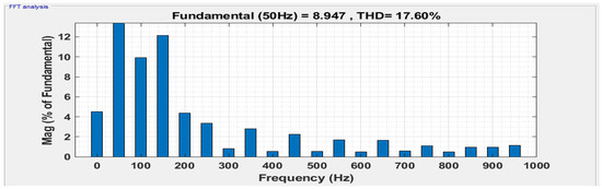
Figure 16.
FFT spectrum of the load current with PD-PWM.
Furthermore, the harmonic profile of load voltages with the POD-PWM and with the APOD-PWM technique are shown in Figure 17 and Figure 18. THD with POD-PWM is calculated as 24.93% and 24.56% with APOD-PWM techniques. The Comparison graph of the harmonic spectrum is shown in Figure 19. The obtained results of three PWM techniques have been compared. It is observed that minimum harmonics are obtained with the PD-PWM technique as of 23.82%.
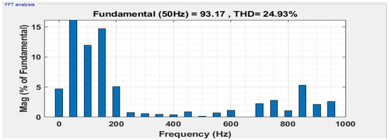
Figure 17.
FFT spectrum of the load voltage with POD-PWM.
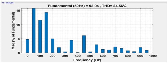
Figure 18.
FFT spectrum of the load voltage with APOD-PWM.
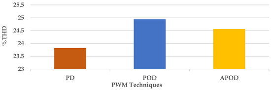
Figure 19.
Comparison graph of PD, POD, and APOD PWM techniques.
6. Discussion
It is evident from the simulation results contained in the precedent section that the proposed new topology of a symmetric nine-level inverter integrated with PV provides improved performance. In this study, PV irradiance varies from 1000 to 800 from 0.04 s to 0.14 s. It is observed that load voltage and load current remain constant with respect to irradiance. As such, PI controllers are implemented with boost converters to maintain the constant output, revealing the constant output of the MLI-fed PV. The THD under the proposed topology is 23.82% with PD-PWM. The THD under the proposed topology is 23.82% with PD-PWM. With a resistive-inductive load, the load current waveform differs from the voltage waveform. According to the inductor value utilized, the current is smoothed due to inductive load. The magnitude of the load current slightly decreases while the load voltage remains approximately constant. Since the current output waveform is closer to a purely sinusoidal, the THD has dropped to 17.60%. However, the THD for the voltage generally remains the same whether an inductive or resistive load is being powered. In addition, THD with POD-PWM is calculated as 24.93% and 24.56% with APOD-PWM techniques. The reduction of harmonics at the output of the new topology has been obtained with the PD-PWM technique. In addition, this new topology of MLI has also been compared with existing topologies. The comparison results reveal improved as of 5, CC/L as of 2.33, CF of 8.66 and 10.66, which are lesser than the existing topologies.
7. Conclusions
This study proposed a new topology of nine-level symmetric MLI for the PV system. The critical aspects addressed through this topology include high , high-cost function, and high components count per level, common problems associated with the existing MLI topologies. As such, this new topology of MLI with reduced device count, minimum , and less cost function has been designed. The proposed topology reveals a of 5, component count per level of 2.33, and a cost function of 8.66 for a cost coefficient of 0.5 and 10.66 for a cost coefficient of 1.5. These results are sufficiently better than the existing topologies. The new topology of MLI has been integrated with the PV system with PI controllers to maintain the constant output of the proposed topology of the MLI under variations in irradiance. The simulation results revealed constant load voltage and load current with respect to variation in irradiance. Implementing the PD-PWM techniques in the proposed topology of MLI has also helped to reduce the harmonics, which are calculated to be 23.82% with PD-PWM. When tested with resistive-inductive load, the proposed topology works decently under resistive-inductive load. The magnitude of the load current slightly decreases while the load voltage remains constant. Since the waveform of the load current is closer to a purely sinusoidal, the THD has dropped to 17.60%. However, whether an inductive or a resistive load is being driven, the THD for the load voltage remains the same. In addition, THD with POD-PWM is calculated as 24.93% and 24.56% with APOD-PWM. Minimum harmonics have been obtained with the PD-PWM technique. Hence, the overall performance of the new topology of MLI is better and more appropriate for PV systems.
Author Contributions
Conceptualization, methodology, investigation, writing—review and editing R.M.; data curation, formal analysis, and supervision, M.A.M.; validation and supervision. A.S.L.; validation and supervision, S.A.A.S. All authors have read and agreed to the published version of the manuscript.
Funding
This research received no external funding.
Institutional Review Board Statement
Not applicable.
Informed Consent Statement
Not applicable.
Data Availability Statement
All data are contained within the article.
Acknowledgments
The authors are thankful to the Mehran University of Engineering and Technology, Jamshoro, Pakistan for support to carry out this research work.
Conflicts of Interest
The authors declare no conflict of interest.
References
- Ellabban, O.; Abu-Rub, H.; Blaabjerg, F. Renewable energy resources: Current status, future prospects and their enabling technology. Renew. Sustain. Energy Rev. 2014, 39, 748–764. [Google Scholar] [CrossRef]
- Das, S.R.; Sahoo, A.K.; Dhiman, G.; Singh, K.K.; Singh, A. Photo voltaic integrated multilevel inverter based hybrid filter using spotted hyena optimizer. Comput. Electr. Eng. 2021, 96, 107510. [Google Scholar] [CrossRef]
- Bana, P.R.; Panda, K.P.; Naayagi, R.; Siano, P.; Panda, G. Recently developed reduced switch multilevel inverter for renewable energy integration and drives application: Topologies, comprehensive analysis and comparative evaluation. IEEE Access 2019, 7, 54888–54909. [Google Scholar] [CrossRef]
- Kumar, P.; Kour, M.; Goyal, S.K.; Singh, B.P. Multilevel inverter topologies in renewable energy applications. In Intelligent Computing Techniques for Smart Energy Systems; Springer: Berlin/Heidelberg, Germany, 2020; pp. 891–902. [Google Scholar]
- Das, S.R.; Ray, P.K.; Sahoo, A.K.; Dhiman, G. Application of optimisation technique in PV integrated multilevel inverter for power quality improvement. Comput. Electr. Eng. 2022, 97, 107606. [Google Scholar] [CrossRef]
- Rajalakshmi, S.; Rangarajan, P. Investigation of modified multilevel inverter topology for PV system. Microprocess. Microsyst. 2019, 71, 102870. [Google Scholar] [CrossRef]
- Bughneda, A.; Salem, M.; Richelli, A.; Ishak, D.; Alatai, S. Review of multilevel inverters for PV energy system applications. Energies 2021, 14, 1585. [Google Scholar] [CrossRef]
- Maheswari, K.; Bharanikumar, R.; Arjun, V.; Amrish, R.; Bhuvanesh, M. A comprehensive review on cascaded H-bridge multilevel inverter for medium voltage high power applications. Mater. Today Proc. 2021, 45, 2666–2670. [Google Scholar] [CrossRef]
- Tarassodi, P.; Siadatan, A.; Keshani, M. Single-Phase Multi-Level Inverter Suitable for Symmetrical and Asymmetrical Photovoltaic (PV) Applications. In Proceedings of the 2019 IEEE 28th International Symposium on Industrial Electronics (ISIE), Vancouver, BC, Canada, 12–14 June 2019; IEEE: New York, NY, USA, 2019; pp. 980–984. [Google Scholar]
- Sun, X.; Wang, B.; Zhou, Y.; Wang, W.; Du, H.; Lu, Z. A single DC source cascaded seven-level inverter integrating switched-capacitor techniques. IEEE Trans. Ind. Electron. 2016, 63, 7184–7194. [Google Scholar] [CrossRef]
- Yousofi-Darmian, S.; Barakati, S.M. A new asymmetric multilevel inverter with reduced number of components. IEEE J. Emerg. Sel. Top. Power Electron. 2019, 8, 4333–4342. [Google Scholar] [CrossRef]
- Ali, A.I.; Sayed, M.A.; Mohamed, E.E.; Azmy, A.M. Advanced single-phase nine-level converter for the integration of multiterminal DC supplies. IEEE J. Emerg. Sel. Top. Power Electron. 2018, 7, 1949–1958. [Google Scholar] [CrossRef]
- Booma, N.; Sridhar, N. Nine level cascaded H-bridge multilevel DC-link inverter. In Proceedings of the 2011 International Conference on Emerging Trends in Electrical and Computer Technology, Nagercoil, India, 23–24 March 2011; IEEE: New York, NY, USA, 2011; pp. 315–320. [Google Scholar]
- Nagarajan, R.; Saravanan, M. Performance analysis of a novel reduced switch cascaded multilevel inverter. J. Power Electron. 2014, 14, 48–60. [Google Scholar] [CrossRef]
- Babaei, E.; Laali, S.; Alilu, S. Cascaded multilevel inverter with series connection of novel H-bridge basic units. IEEE Trans. Ind. Electron. 2014, 61, 6664–6671. [Google Scholar] [CrossRef]
- Mokhberdoran, A.; Ajami, A. Symmetric and asymmetric design and implementation of new cascaded multilevel inverter topology. IEEE Trans. Power Electron. 2014, 29, 6712–6724. [Google Scholar] [CrossRef]
- Venkataramanaiah, J.; Suresh, Y.; Panda, A.K. A review on symmetric, asymmetric, hybrid and single DC sources based multilevel inverter topologies. Renew. Sustain. Energy Rev. 2017, 76, 788–812. [Google Scholar] [CrossRef]
- Venkatraman, T.; Periasamy, S. Multilevel inverter topology with modified pulse width modulation and reduced switch count. Acta Polytech. Hung. 2018, 15, 141–167. [Google Scholar]
- Alishah, R.S.; Hosseini, S.H.; Babaei, E.; Sabahi, M. A new general multilevel converter topology based on cascaded connection of submultilevel units with reduced switching components, DC sources, and blocked voltage by switches. IEEE Trans. Ind. Electron. 2016, 63, 7157–7164. [Google Scholar] [CrossRef]
- Sadanala, C.; Pattnaik, S.; Singh, V.P. A flying capacitor based multilevel inverter architecture with symmetrical and asymmetrical configurations. IEEE J. Emerg. Sel. Top. Power Electron. 2020, 10, 2210–2222. [Google Scholar] [CrossRef]
- Firdous, Z.; Rehman, H.; Tariq, M.; Sarwar, A. Investigation of Fault-Tolerant Capabilities of a Reduced Device Multilevel Inverter. In Proceedings of the 2022 2nd International Conference on Emerging Frontiers in Electrical and Electronic Technologies (ICEFEET), Patna, India, 24–25 June 2022; IEEE: New York, NY, USA, 2022; pp. 1–5. [Google Scholar]
- Ali, M.; Tariq, M.; Sarwar, A.; Alamri, B. A 13-, 11-, and 9-Level Boosted Operation of a Single-Source Asymmetrical Inverter with Hybrid PWM Scheme. IEEE Trans. Ind. Electron. 2022, 69, 12817–12828. [Google Scholar] [CrossRef]
- Upadhyay, D.; Ali, M.; Tariq, M.; Khan, S.A.; Alamri, B.; Alahmadi, A. Thirteen-level UXE-type inverter with 12-band hysteresis current control employing PSO based PI controller. IEEE Access 2022, 10, 29890–29902. [Google Scholar] [CrossRef]
- Asif, M.; Tariq, M.; Sarwar, A.; Hussan, M.R.; Ahmad, S.; Mihet-Popa, L.; Shah Noor Mohamed, A. A Robust Multilevel Inverter Topology for Operation under Fault Conditions. Electronics 2021, 10, 3099. [Google Scholar] [CrossRef]
- Wasiq, M.; Sarwar, A.; Sarwer, Z.; Tariq, M.; Ahmad, S.; Al-Shayea, A.M.; Hossain, J. Design and Validation of a Reduced Switching Components Step-Up Multilevel Inverter (RSCS-MLI). Processes 2021, 9, 1948. [Google Scholar] [CrossRef]
- Ponnusamy, P.; Sivaraman, P.; Almakhles, D.J.; Padmanaban, S.; Leonowicz, Z.; Alagu, M.; Ali, J.S.M. A new multilevel inverter topology with reduced power components for domestic solar PV applications. IEEE Access 2020, 8, 187483–187497. [Google Scholar] [CrossRef]
- Rubeena, A.; Paulose, S.; Thomas, M.; Joy, J. PWM control strategies for Switched-Capacitor inverters. Mater. Today Proc. 2022, 58, 516–522. [Google Scholar]
- Samadaei, E.; Sheikholeslami, A.; Gholamian, S.A.; Adabi, J. A square T-type (ST-Type) module for asymmetrical multilevel inverters. IEEE Trans. Power Electron. 2017, 33, 987–996. [Google Scholar] [CrossRef]
- Khasim, S.R.; Dhanamjayulu, C. Design and Implementation of Asymmetrical Multilevel Inverter with Reduced Components and Low Voltage Stress. IEEE Access 2022, 10, 3495–3511. [Google Scholar] [CrossRef]
- Prabaharan, N.; Palanisamy, K. Analysis of cascaded H-bridge multilevel inverter configuration with double level circuit. IET Power Electron. 2017, 10, 1023–1033. [Google Scholar] [CrossRef]
- Pradhan, A.; Panda, B. A simplified design and modeling of boost converter for photovoltaic sytem. Int. J. Electr. Comput. Eng. 2018, 8, 141. [Google Scholar] [CrossRef]
- Sarker, R. Phase Opposition Disposition PWM (POD-PWM) Strategy to Reduce WTHD Content from an NPC Inverter-Fed Electric Vehicle System. In Proceedings of the 2020 IEEE 17th India Council International Conference (INDICON), New Delhi, India, 10–13 December 2020; IEEE: New York, NY, USA, 2020; pp. 1–6. [Google Scholar]
- Thakre, K.; Mohanty, K.B. Performance improvement of multilevel inverter through trapezoidal triangular carrier based PWM. In Proceedings of the 2015 International Conference on Energy, Power and Environment: Towards Sustainable Growth (ICEPE), Shillong, India, 12–13 June 2015; IEEE: New York, NY, USA, 2015; pp. 1–6. [Google Scholar]
- Jagabar Sathik, M.A.; Abdel Aleem, S.H.E.; Kannan, R.; Zobaa, A.F. A new switched DC-link capacitor-based multi-level converter (SDC2MLC). Electr. Power Compon. Syst. 2017, 45, 1001–1015. [Google Scholar] [CrossRef]
- Alishah, R.S.; Hosseini, S.H.; Babaei, E.; Sabahi, M. Optimal design of new cascaded switch-ladder multilevel inverter structure. IEEE Trans. Ind. Electron. 2016, 64, 2072–2080. [Google Scholar] [CrossRef]
- Alishah, R.S.; Hosseini, S.H.; Babaei, E.; Sabahi, M.; Gharehpetian, G.B. New high step-up multilevel converter topology with self-voltage balancing ability and its optimization analysis. IEEE Trans. Ind. Electron. 2017, 64, 7060–7070. [Google Scholar] [CrossRef]


Disclaimer/Publisher’s Note: The statements, opinions and data contained in all publications are solely those of the individual author(s) and contributor(s) and not of MDPI and/or the editor(s). MDPI and/or the editor(s) disclaim responsibility for any injury to people or property resulting from any ideas, methods, instructions or products referred to in the content. |
© 2023 by the authors. Licensee MDPI, Basel, Switzerland. This article is an open access article distributed under the terms and conditions of the Creative Commons Attribution (CC BY) license (https://creativecommons.org/licenses/by/4.0/).