


An Efficacious Modulation Gambit Using Fewer Switches in a Multilevel Inverter


 ,
, 

Abstract
:1. Introduction
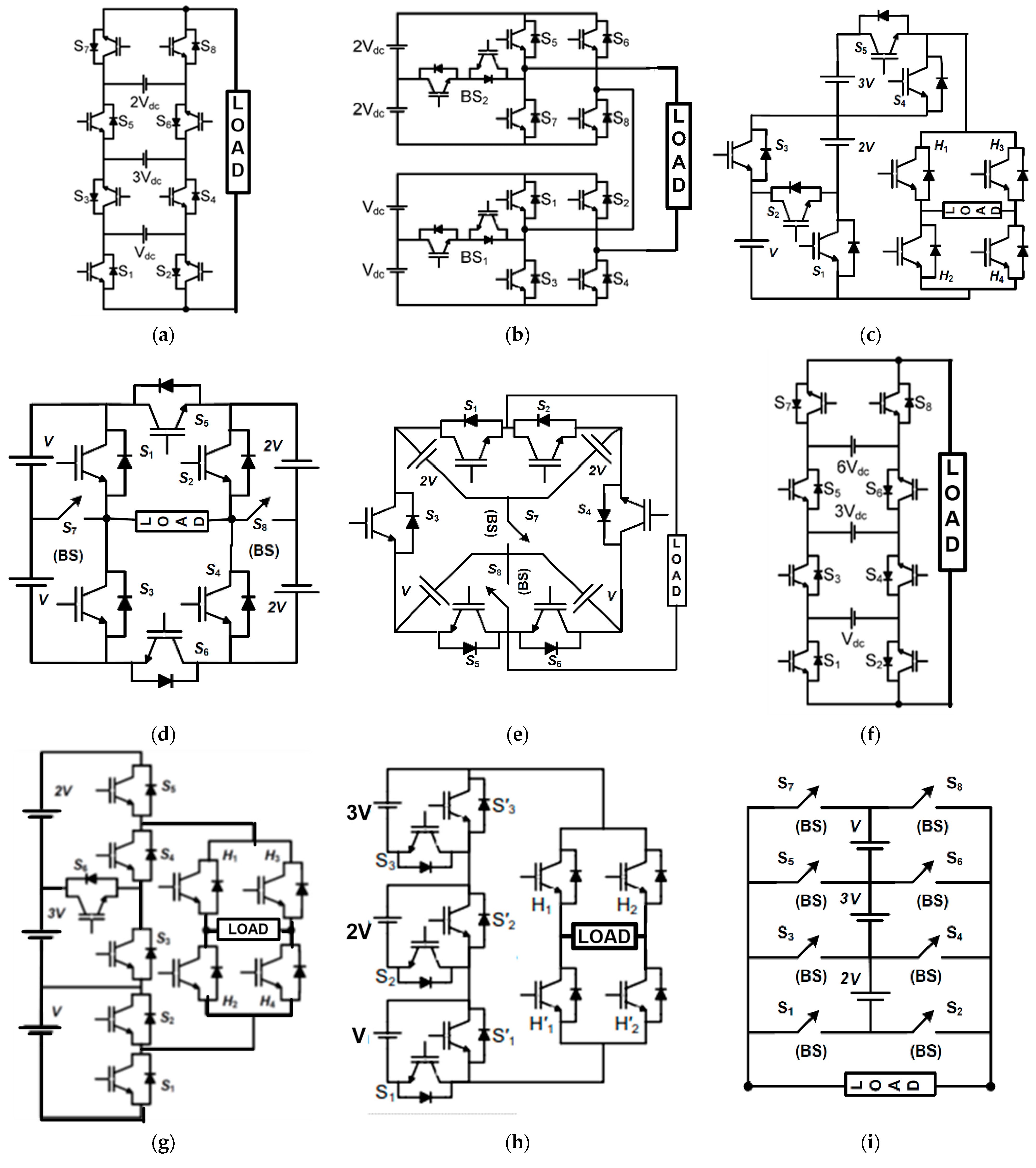
2. RSC MLI Topologies and Their Modulation Schemes
Limitation of Conventional LSPWM to RSC Configurations
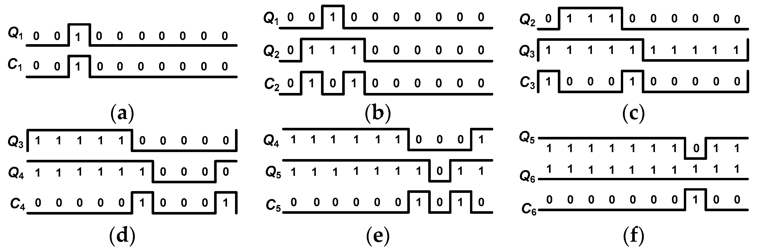
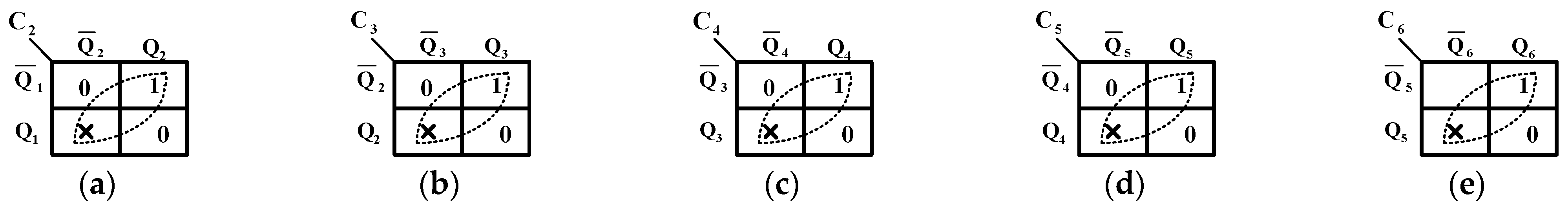
3. Proposed Generalized LSPWM Scheme
4. Implementation of Proposed Scheme to Various 13-Level RSC MLIs
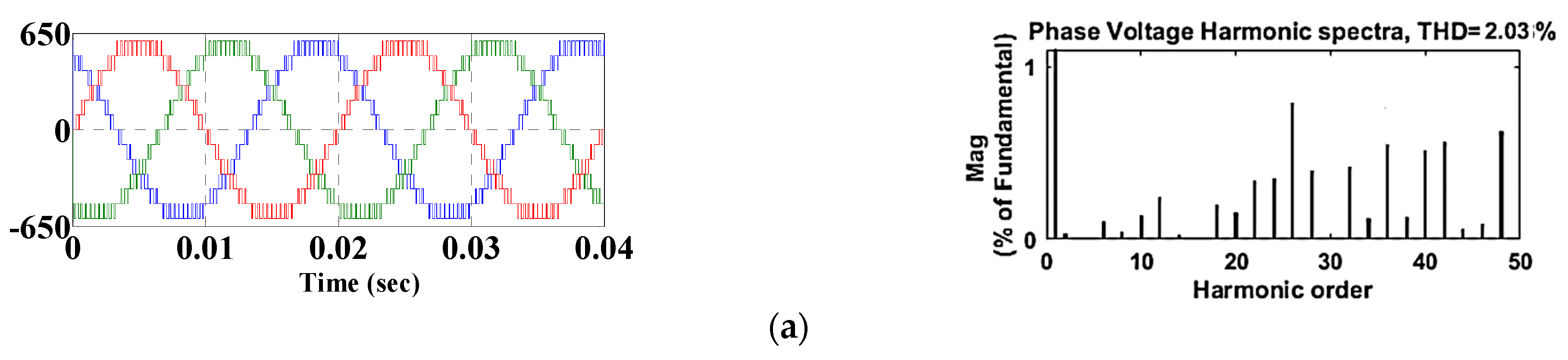
5. Experimental Results
6. Conclusions
Author Contributions
Funding
Institutional Review Board Statement
Informed Consent Statement
Conflicts of Interest
References
- Lai, J.S.; Peng, F.Z. Multilevel converters-a new breed of power converters. IEEE Trans. Ind. Appl. 1996, 32, 509–517. [Google Scholar]
- Kouro, S.; Malinowski, M.; Gopakumar, K.; Pou, J.; Franquelo, L.G.; Wu, B.; Rodriguez, J.; Pérez, M.A.; Leon, J.I. Recent advances and industrial applications of multilevel converters. IEEE Trans. Ind. Electron. 2010, 57, 2553–2580. [Google Scholar] [CrossRef]
- Rodriguez, J.; Lai, J.S.; Peng, F.Z. Multilevel inverters: A survey of topologies, controls, and applications. IEEE Trans. Ind. Electron. 2002, 49, 724–738. [Google Scholar] [CrossRef]
- Franquelo, L.G.; Rodriguez, J.; Leon, J.I.; Kouro, S.; Portillo, R.; Prats, M.A. The age of multilevel converters arrives. IEEE Ind. Electron. Mag. 2008, 2, 28–39. [Google Scholar] [CrossRef]
- Carrara, G.; Gardella, S.; Marchesoni, M.; Salutari, R.; Sciutto, G. A new multilevel PWM method: A theoretical analysis. IEEE Trans. Power Electron. 1992, 7, 497–505. [Google Scholar] [CrossRef]
- McGrath, B.P.; Holmes, D.G. Multicarrier PWM strategies for multilevel inverters. IEEE Trans. Ind. Electron. 2002, 49, 858–867. [Google Scholar] [CrossRef]
- Sreenivasarao, D.; Agarwal, P.; Das, B. Performance evaluation of carrier rotation strategy in level-shifted pulse-width modulation technique. IET Power Electron. 2014, 7, 667–680. [Google Scholar] [CrossRef]
- Bassi, H.M.; Salam, Z. A new hybrid multilevel inverter topology with reduced switch count and DC voltage sources. Energies 2019, 12, 977. [Google Scholar] [CrossRef]
- Omer, P.; Kumar, J.; Surjan, B.S. A Review on Reduced Switch Count Multilevel Inverter Topologies. IEEE Access 2020, 8, 22281–22302. [Google Scholar] [CrossRef]
- Vemuganti, H.P.; Sreenivasarao, D.; Ganjikunta, S.K.; Suryawanshi, H.M.; Abu-Rub, H. A survey on reduced switch count multilevel inverters. IEEE Open J. Ind. Electron. Soc. 2021, 2, 80–111. [Google Scholar] [CrossRef]
- Sunddararaj, S.P.; Srinivasarangan Rangarajan, S. An extensive review of multilevel inverters based on their multifaceted structural configuration, triggering methods and applications. Electronics 2020, 9, 433. [Google Scholar] [CrossRef]
- Kumawat, R.K.; Palwalia, D.K. A comprehensive analysis of reduced switch count multilevel inverter. Aust. J. Electr. Electron. Eng. 2020, 17, 13–27. [Google Scholar] [CrossRef]
- Sathik, M.J.; Sandeep, N.; Almakhles, D.; Blaabjerg, F. Cross Connected Compact Switched-Capacitor Multilevel Inverter (C3-SCMLI) Topology with Reduced Switch Count. IEEE Trans. Circuits Syst. II Express Briefs 2020, 67, 3287–3291. [Google Scholar]
- Taheri, A.; Rasulkhani, A.; Ren, H.-P. An asymmetric switched capacitor multilevel inverter with component reduction. IEEE Access 2019, 7, 127166–127176. [Google Scholar] [CrossRef]
- Su, G.-J. Multilevel DC-link inverter. IEEE Trans. Ind. Appl. 2005, 41, 848–854. [Google Scholar] [CrossRef]
- Sanjeevan, A.R.; Kaarthik, R.S.; Gopakumar, K.; Rajeevan, P.; Leon, J.I.; Franquelo, L.G. Reduced common-mode voltage operation of a new seven-level hybrid multilevel inverter topology with a single DC voltage source. IET Power Electron. 2016, 9, 519–528. [Google Scholar] [CrossRef]
- Babaei, E. A cascade multilevel converter topology with reduced number of switches. IEEE Trans. Power Electron. 2008, 23, 2657–2664. [Google Scholar] [CrossRef]
- Najafi, E.; Yatim, A.H.M. Design and implementation of a new multilevel inverter topology. IEEE Trans. Ind. Electron. 2012, 59, 4148–4154. [Google Scholar] [CrossRef]
- Gupta, K.K.; Jain, S. A novel multilevel inverter based on switched DC sources. IEEE Trans. Ind. Electron. 2014, 61, 3269–3278. [Google Scholar] [CrossRef]
- Babaei, E.; Laali, S.; Bayat, Z. A single-phase cascaded multilevel inverter based on a new basic unit with reduced number of power switches. IEEE Trans. Ind. Electron. 2015, 62, 922–929. [Google Scholar] [CrossRef]
- Samadaei, E.; Gholamian, S.A.; Sheikholeslami, A.; Adabi, J. An envelope type (E-Type) module: Asymmetric multilevel inverters with reduced components. IEEE Trans. Ind. Electron. 2016, 63, 7148–7156. [Google Scholar] [CrossRef]
- Park, S.-J.; Kang, F.-S.; Lee, M.H.; Kim, C.-U. A new single-phase five-level PWM inverter employing a deadbeat control scheme. IEEE Trans. Power Electron. 2003, 18, 831–843. [Google Scholar] [CrossRef]
- Choi, J.-S.; Kang, F.-S. Seven-level PWM inverter employing series-connected capacitors paralleled to a single DC voltage source. IEEE Trans. Ind. Electron. 2015, 62, 3448–3459. [Google Scholar]
- Rahim, N.A.; Chaniago, K.; Selvaraj, J. Single-phase seven-level grid-connected inverter for photovoltaic system. IEEE Trans. Ind. Electron. 2011, 58, 2435–2443. [Google Scholar] [CrossRef]
- Alishah, R.S.; Nazarpour, D.; Hosseini, S.H.; Sabahi, M. Reduction of power electronic elements in multilevel converters using a new cascade structure. IEEE Trans. Ind. Electron. 2015, 62, 256–269. [Google Scholar] [CrossRef]
- Rahim, N.A.; Elias, M.F.M.; Hew, W.P. Transistor-clamped H-bridge based cascaded multilevel inverter with new method of capacitor voltage balancing. IEEE Trans. Ind. Electron. 2013, 60, 2943–2956. [Google Scholar]
- Gautam, S.P.; Kumar, L.; Gupta, S. Hybrid topology of symmetrical multilevel inverter using less number of devices. IET Power Electron. 2015, 8, 2125–2135. [Google Scholar] [CrossRef]
- Gautam, S.P.; Sahu, L.K.; Gupta, S. Reduction in number of devices for symmetrical and asymmetrical multilevel inverters. IET Power Electron. 2016, 9, 698–709. [Google Scholar] [CrossRef]
- Choi, W.K.; Kang, F.S. H-bridge based multilevel inverter using PWM switching function. In Proceedings of the INTELEC 2009—31st International Telecommunications Energy Conference, Incheon, Republic of Korea, 18–22 October 2009; pp. 1–5. [Google Scholar]
- Hinago, Y.; Koizumi, H. A single-phase multilevel inverter using switched series/parallel DC voltage sources. IEEE Trans. Ind. Electron. 2010, 57, 2643–2650. [Google Scholar] [CrossRef]
- Hinago, Y.; Koizumi, H. A switched-capacitor inverter using series/parallel conversion with inductive load. IEEE Trans. Ind. Electron. 2012, 59, 878–887. [Google Scholar] [CrossRef]
- dos Santos, E.C.; Muniz, J.H.G.; da Silva, E.R.C.; Jacobina, C.B. Nested multilevel topologies. IEEE Trans. Power Electron. 2015, 30, 4058–4068. [Google Scholar] [CrossRef]
- Barzegarkhoo, R.; Zamiri, E.; Vosoughi, N.; Kojabadi, H.M.; Chang, L. Cascaded multilevel inverter using series connection of novel capacitor-based units with minimum switch count. IET Power Electron. 2016, 9, 2060–2075. [Google Scholar] [CrossRef]
- Babaei, E.; Gowgani, S.S. Hybrid multilevel inverter using switched capacitor units. IEEE Trans. Ind. Electron. 2014, 61, 4614–4621. [Google Scholar] [CrossRef]
- Babaei, E.; Kangarlu, M.F.; Hosseinzadeh, M.A. Asymmetrical multilevel converter topology with reduced number of components. IET Power Electron. 2013, 6, 1188–1196. [Google Scholar] [CrossRef]
- Odeh, C.I. A cascaded multi-level inverter topology with improved modulation scheme. Electr. Power Compon. Syst. 2014, 42, 768–777. [Google Scholar] [CrossRef]
- Babaei, E.; Laali, S.; Alilu, S. Cascaded multilevel inverter with series connection of novel H-bridge basic units. IEEE Trans. Ind. Electron. 2014, 61, 6664–6671. [Google Scholar] [CrossRef]
- Odeh, C.I.; Obe, E.S.; Ojo, O. Topology for cascaded multilevel inverter. IET Power Electron. 2016, 9, 921–929. [Google Scholar] [CrossRef]
- Masaoud, A.; Ping, H.W.; Mekhilef, S.; Taallah, A.S. New three-phase multilevel inverter with reduced number of power electronic components. IEEE Trans. Power Electron. 2014, 29, 6018–6029. [Google Scholar] [CrossRef]
- Salem, A.; Ahmed, E.M.; Orabi, M.; Ahmed, M. New three-phase symmetrical multilevel voltage source inverter. IEEE J. Emerg. Sel. Top. Circuits Syst. 2015, 5, 430–442. [Google Scholar] [CrossRef]
- Masaoud, A.; Ping, H.W.; Mekhilef, S.; Taallah, A. Novel configuration for multilevel DC-link three-phase five-level inverter. IET Power Electron. 2014, 7, 3052–3061. [Google Scholar] [CrossRef]
- Thiyagarajan, V. A New Symmetric and Asymmetric Multilevel Inverter Circuit with Reduced Number of Components. Mater. Proc. 2022, 10, 5. [Google Scholar]
- Srinivasan, G.K.; Rivera, M.; Loganathan, V.; Ravikumar, D.; Mohan, B. Trends and Challenges in Multi-Level Inverter with Reduced Switches. Electronics 2021, 10, 368. [Google Scholar] [CrossRef]
- Islam, M.T.; Fayek, H.H.; Rusu, E.; Rahman, M.F. A Novel Hexagonal-Shaped Multilevel Inverter with Reduced Switches for Grid-Integrated Photovoltaic System. Sustainability 2021, 13, 12018. [Google Scholar] [CrossRef]
- Azimi, E.; Khodaparast, A.; Rostami, M.J.; Adabi, J.; Adabi, M.E.; Rezanejad, M.; Rodrigues, E.M.G.; Pouresmaeil, E. X-Type Step-Up Multi-Level Inverter with Reduced Component Count Based on Switched-Capacitor Concept. Electronics 2020, 9, 1987. [Google Scholar] [CrossRef]
- Wasiq, M.; Sarwar, A.; Sarwer, Z.; Tariq, M.; Ahmad, S.; Al-Shayea, A.M.; Hossain, J. Design and Validation of a Reduced Switching Components Step-Up Multilevel Inverter (RSCS-MLI). Processes 2021, 9, 1948. [Google Scholar] [CrossRef]
- Andela, M.; Shaik, A.; Beemagoni, S.; Kurimilla, V.; Veramalla, R.; Kodakkal, A.; Salkuti, S.R. Solar Photovoltaic System-Based Reduced Switch Multilevel Inverter for Improved Power Quality. Clean Technol. 2022, 4, 1–13. [Google Scholar] [CrossRef]
- Rech, C.; Pinheiro, J.R. Hybrid multilevel converters: Unified analysis and design considerations. IEEE Trans. Ind. Electron. 2007, 54, 1092–1104. [Google Scholar] [CrossRef]
- Vemuganti, H.P.; Sreenivasarao, D.; Kumar, G.S.; Spandana, A.S. Reduced carrier PWM scheme with unified logical expressions for reduced switch count multilevel inverters. IET Power Electron. 2018, 11, 912–921. [Google Scholar] [CrossRef]
- Vemuganti, H.P.; Sreenivasarao, D.; Siva Kumar, G. Improved pulse-width modulation scheme for T-type multilevel inverter. IET Power Electron. 2017, 10, 968–976. [Google Scholar] [CrossRef]
- Faiz Minai, A.; Khan, A.A.; Pachauri, R.K.; Malik, H.; García Márquez, F.P.; Arcos Jiménez, A. Performance Evaluation of Solar PV-Based Z-Source Cascaded Multilevel Inverter with Optimized Switching Scheme. Electronics 2022, 11, 3706. [Google Scholar] [CrossRef]


| Topology | Topology Description | Symmetrical/ Asymmetrical | Modulation Schemes Reported in Literature | Demerits of the Modulation Scheme | |
|---|---|---|---|---|---|
| Symmetrical | Asymmetrical | ||||
| MLDCL [13] | Separate level and polarity generators | Both | Low-frequency switching scheme | Complicated at higher levels and poor THD | |
| PUC [14] | Can be extended with and without cascading | Both | SVPWM | Complicated at higher levels | |
| CBSC [15] | Can be extended with and without cascading | Both | Low-frequency switching scheme | Complicated at higher levels and poor THD | |
| RV [16] | Separate level and polarity generators | Symmetrical | Reduced carrier PWM | Poor THD in line voltage | |
| Switched DC sources [17] | Involves separate DC link for all phases | Both | Switching function PWM | Increased comparisons at higher levels | |
| SSPS [28,29] | Separate level and polarity generators | Both | LSPWM with maximum and minimum conditions [29] | Hybrid PWM [28] | Increased comparisons at higher levels [29] |
| SCSS [27] | Separate level and polarity generators | Symmetrical | Switching function PWM at low frequency | Complicated at higher levels | |
| T-type [20,21,22,23,24] | T-type: Extended without cascading [21,22] | Symmetrical | Multi reference PWM [22] Reduced carrier with logic gates [20,21] | Poor THD in line voltages [20,21,22] | |
| T-Type | Both | Modified reduced carrier PWM [50,51] | Synchronized PWM: Produces degraded line THD, if (fcr) ≠ 3n*fs fcr: carrier frequency & fs = modulating frequency | ||
| Cascaded T-type: Extended with and without cascading [23,24] | Both | Fundamental frequency switching [23] Phase shifted multi reference [24] | Complicated at higher levels [23] and poor THD [23,24] | ||
| Basic unit MLI [18] | Separate level and polarity generators | Both | An algorithm based PWM | Complicated at higher levels and poor THD | |
| Nested cell [30] | Common DC link to all phases | Both | SVPWM | Complicated at higher levels | |
| Hybrid T-type [25,26] | Can be extended with and without cascading | Both | Low-frequency carrier switching [25,26] | Low-frequency switching [26] | Complicated at higher levels and poor THD [25,26] |
| E-type [19] | Extended by cascading | Asymmetrical | SHE | Complicated at higher levels and slow dynamic response | |
| Reduced cascaded [33,34,35,36] | Extended to higher level by cascading | Both [33,35] | Hybrid PWM [33] | ||
| Symmetrical [34] | Multi-reference with logic gates [34] | Complicated at higher levels and poor THD | |||
| Asymmetrical [36] | Multi reference with low-frequency carrier [36] | Complicated at higher levels and poor THD | |||
| Switched capacitor hybrid MLI [32] | Extended by cascading or series connection of capacitor units | Symmetrical | Fundamental switching scheme | Complicated at higher levels and poor THD | |
| Basic capacitor unit MLI [31] | Extended by series connection of capacitor units | Both | Hybrid PWM | ||
| RSC MLI with three phases [37,38,39] | With common DC link to three phases [37,39] | Asymmetrical [37,39] | Low-frequency reduced carrier using logical operators [38] | SVPWM [37,39] | Complicated at higher levels [37,39] and poor THD [38] |
| Separate DC link to three-phases [38] | Symmetrical [38] | ||||
| Voltage Level | MLDCL | CBSC | PUC | Hybrid T-Type | E-Type | Switched DC Sources | Cascaded T-Type | SSPS | RV |
|---|---|---|---|---|---|---|---|---|---|
| 0 | S2-S4-S6-H1-H4 S2-S4-S6-H3-H2 H1-H3 H2-H4 | S1-S2 S3-S4 S5-S6 S7-S8 | S8-S6-S4-S2 S1-S3-S5-S7 | S3-S6-S4 S1-S5-S2 | S6-S4-S2 S5-S3-S1 | S4-S3-S2-S1 S5-S6-S7-S8 | H4-H2-H8-H6 H1-H7-H5-H3 | H1-H3 H3-H2 | S2-S3-S4-H1-H4 S2-S3-S4-H3-H2 H1-H3 H2-H4 |
| V | S4-S6-H1-H4-S1 | S7-S6 | S5-S3-S1-S8 | S7-S4-S6 | S4-S3-S8 | S3-S2-S1-S5 | S1-H8-H6-H4 | S3-S4-H1-H4 | S3-S4-H1-H4-S1 |
| 2 V | S6-H1-H4-S2-S3 | S3-S2 | S3-S1-S7-S6 | S1-S4-S6 S6-S3-S8 | S1-S8-S7 S4-S2-S5 | S1-S5-S6-S7 | H1-H8-H6-H4 S2-H4-H2-H8 | S4-H1-H4-S1 | S5-H1-H4-S2-S3-S6 |
| 3 V | S6-H1-H4-S1-S3 H1-H4-S2-S4-S5 | S5-S4 | S3-S1-S8-S6 | S7-S8-S6 | S5-S7-S1 | S7-S8-S4-S3 | S1-H8-S2-H4 | S4-H1-H4-S2 | S6-S4-H1-H4-S2 |
| 4 V | H1-H4-S1-S4-S5 | S7-S4 | S1-S8-S5-S4 | S1-S8-S6 | S1-S6-S4 | S7-S8-S5-S3 | H1-H8-S2-H4 S5-H4-H2-H8 | S5-H1-H4-S3 | S6-S4-H1-H4-S1 |
| 5 V | H1-H4-S2-S3-S5 | S5-S2 | S1-S7-S6-S4 | S7-S2-S6 | S1-S8-S4 | S1-S4-S3-S7 | S1-H8-H5-H4 | S5-H1-H4-S1 | S5-H1-H4-S2 |
| 6 V | H1-H4-S1-S3-S5 | S7-S2 | S1-S8-S6-S4 | S1-S2-S6 | S1-S5-S4 | S1-S5-S3-S7 | H1-H8-H5-H4 | S5-H1-H4-S2 | S5-H1-H4-S1 |
| −V | S4-S6-H2-H3-S1 | S8-S5 | S6-S4-S2-S7 | S5-S2-S7 | S3-S1-S8 | S6-S7-S8-S4 | H3-H5-H7-S1 | S3-S4-H3-H2 | S3-S4-H3-H2-S1 |
| −2 V | S6-H3-H2-S2-S3 | S4-S1 | S4-S2-S8-S5 | S5-S2-S3 S5-S1-S8 | S2-S8-S7 S3-S1-S6 | S8-S4-S3-S2 | H3-H5-H7-H2 H7-H1-H3-S2 | S4-H3-H2-S1 | S5-H3-H2-S2-S3-S6 |
| −3 V | S6-H3-H2-S1-S3 H3-H2-S2-S4-S5 | S6-S3 | S4-S2-S7-S5 | S5-S8-S7 | S2-S6-S7 | S2-S1-S5-S6 | H3-S2-H7-S1 | S4-H3-H2-S2 | S6-S4-H3-H2-S2 |
| −4 V | H3-H2-S1-S4-S5 | S8-S3 | S2-S7-S6-S3 | S4-S1-S5 | S2-S5-S3 | S2-S1-S4-S6 | H7-H1-H3-H6 H3-S2-H7-H2 | S5-H3-H2-S3 | S6-S4-H3-H2-S1 |
| −5 V | H3-H2-S2-S3-S5 | S6-S1 | S2-S8-S5-S3 | S7-S5-S4 | S2-S8-S3 | S8-S5-S6-S2 | H3-H6-H7-S1 | S5-H3-H2-S1 | S5-H3-H2-S2 |
| −6 V | H3-H2-S1-S3-S5 | S8-S1 | S2-S7-S5-S3 | S4-S3-S5 | S2-S6-S3 | S8-S4-S6-S2 | H3-H6-H7-H2 | S5-H3-H2-S2 | S5-H3-H2-S1 |
| Q1 | Q2 | Q3 | Q4 | Q5 | Q6 | Q7 | Q8 | Q9 | Q10 | Q11 | Q12 | C1 | C2 | C3 | C4 | C5 | C6 | C7 | C8 | C9 | C10 | C11 | C12 |
|---|---|---|---|---|---|---|---|---|---|---|---|---|---|---|---|---|---|---|---|---|---|---|---|
| 1 | 1 | 1 | 1 | 1 | 1 | 1 | 1 | 1 | 1 | 1 | 0 | 1 | 0 | 0 | 0 | 0 | 0 | 0 | 0 | 0 | 0 | 0 | 0 |
| 0 | 1 | 1 | 1 | 1 | 1 | 1 | 1 | 1 | 1 | 1 | 0 | 0 | 1 | 0 | 0 | 0 | 0 | 0 | 0 | 0 | 0 | 0 | 0 |
| 0 | 0 | 1 | 1 | 1 | 1 | 1 | 1 | 1 | 1 | 1 | 0 | 0 | 0 | 1 | 0 | 0 | 0 | 0 | 0 | 0 | 0 | 0 | 0 |
| 0 | 0 | 0 | 1 | 1 | 1 | 1 | 1 | 1 | 1 | 1 | 0 | 0 | 0 | 0 | 1 | 0 | 0 | 0 | 0 | 0 | 0 | 0 | 0 |
| 0 | 0 | 0 | 0 | 1 | 1 | 1 | 1 | 1 | 1 | 1 | 0 | 0 | 0 | 0 | 0 | 1 | 0 | 0 | 0 | 0 | 0 | 0 | 0 |
| 0 | 0 | 0 | 0 | 0 | 1 | 1 | 1 | 1 | 1 | 1 | 0 | 0 | 0 | 0 | 0 | 0 | 1 | 0 | 0 | 0 | 0 | 0 | 0 |
| 0 | 0 | 0 | 0 | 0 | 0 | 1 | 1 | 1 | 1 | 1 | 0 | 0 | 0 | 0 | 0 | 0 | 0 | 1 | 0 | 0 | 0 | 0 | 0 |
| 0 | 0 | 0 | 0 | 0 | 0 | 0 | 1 | 1 | 1 | 1 | 0 | 0 | 0 | 0 | 0 | 0 | 0 | 0 | 1 | 0 | 0 | 0 | 0 |
| 0 | 0 | 0 | 0 | 0 | 0 | 0 | 0 | 1 | 1 | 1 | 0 | 0 | 0 | 0 | 0 | 0 | 0 | 0 | 0 | 1 | 0 | 0 | 0 |
| 0 | 0 | 0 | 0 | 0 | 0 | 0 | 0 | 0 | 1 | 1 | 0 | 0 | 0 | 0 | 0 | 0 | 0 | 0 | 0 | 0 | 1 | 0 | 0 |
| 0 | 0 | 0 | 0 | 0 | 0 | 0 | 0 | 0 | 0 | 1 | 0 | 0 | 0 | 0 | 0 | 0 | 0 | 0 | 0 | 0 | 0 | 1 | 0 |
| 0 | 0 | 0 | 0 | 0 | 0 | 0 | 0 | 0 | 0 | 0 | 1 | 0 | 0 | 0 | 0 | 0 | 0 | 0 | 0 | 0 | 0 | 0 | 1 |
| Conduction Interval (Ci) | State of Switching Pulse (Pi) | Switching Devices to Be Selected to Obtain Required Voltage | ||||
|---|---|---|---|---|---|---|
| MLDCL | CBSC | PUC | Hybrid T-Type | E-Type | ||
| C1 = 1 (5 V to 6 V) band | P1 =1 (6 V state) | S3-S5-H1-H4-S1 | S7-S2 | S1-S8-S6-S4 | S1-S2-S6 | S1-S5-S4 |
| P1 =0 (5 V state) | S5-H1-H4-S2-S3 | S5-S2 | S1-S7-S6-S4 | S7-S2-S6 | S1-S8-S4 | |
| C2 = 1 (4 V to 5 V) band | P2 =1 (5 V state) | S5-H1-H4-S2-S3 | S5-S2 | S1-S7-S6-S4 | S7-S2-S6 | S1-S8-S4 |
| P2 = 0 (4 V state) | S4-S5-H1-H4-S1 | S7-S4 | S1-S8-S5-S4 | S1-S8-S6 | S1-S6-S4 | |
| C3 = 1 (3 V to 4 V) band | P3 = 1 (4 V state) | S4-S5-H1-H4-S1 | S7-S4 | S1-S8-S5-S4 | S1-S8-S6 | S1-S6-S4 |
| P3 = 0 (3 V state) | H1-H4-S2-S4-S5 | S5-S4 | S3-S1-S8-S6 | S7-S8-S6 | S5-S7-S1 | |
| C4 = 1 (2 V to 3 V) band | P4 = 1 (3 V state) | H1-H4-S2-S4-S5 | S5-S4 | S3-S1-S8-S6 | S7-S8-S6 | S5-S7-S1 |
| P4 = 0 (2 V state) | S6-H1-H4-S2-S3 | S3-S2 | S3-S1-S7-S6 | S1-S4-S6 | S1-S8-S7 | |
| C5 = 1 (V to 2 V) band | P5 = 1 (2 V state) | S6-H1-H4-S2-S3 | S3-S2 | S3-S1-S7-S6 | S1-S4-S6 | S1-S8-S7 |
| P5 = 0 (V state) | S4-S6-H1-H4-S1 | S7-S6 | S5-S3-S1-S8 | S7-S4-S6 | S4-S2-S8 | |
| C6 = 1 (0 to V) band | P6 = 1 (V state) | S4-S6-H1-H4-S1 | S7-S6 | S5-S3-S1-S8 | S7-S4-S6 | S4-S2-S8 |
| P6 = 0 (0 state) | S2-S4-S6-H1-H4 | S7-S8 | S1-S3-S5-S7 | S4-S6-S3 | S6-S4-S2 | |
| C7 = 1 (−V to 0) band | P7 = 1 (0 state) | S2-S4-S6-H3-H2 | S5-S6 | S1-S3-S5-S7 | S2-S1-S5 | S5-S3-S1 |
| P7 = 0 (−V state) | S4-S6-H3-H2-S1 | S8-S5 | S6-S4-S2-S7 | S5-S2-S7 | S3-S1-S8 | |
| C8 = 1 (−2 V to −V) band | P8 = 1 (−V state) | S4-S6-H3-H2-S1 | S8-S5 | S6-S4-S2-S7 | S5-S2-S7 | S3-S1-S8 |
| P8 = 0 (−2 V state) | S6-H3-H2-S2-S3 | S4-S1 | S4-S2-S8-S5 | S5-S2-S3 | S2-S8-S7 | |
| C9 = 1 (−3 V to −2 V) band | P9 = 1 (−2 V state) | S6-H3-H2-S2-S3 | S4-S1 | S4-S2-S8-S5 | S5-S2-S3 | S2-S8-S7 |
| P9 = 0 (−3 V state) | H3-H2-S2-S4-S5 | S6-S3 | S4-S2-S7-S5 | S5-S8-S7 | S2-S6-S7 | |
| C10 = 1 (−4 V to −3 V) band | P10 = 1 (−3 V state) | H3-H2-S2-S4-S5 | S6-S3 | S4-S2-S7-S5 | S5-S8-S7 | S2-S6-S7 |
| P10 = 0 (−4 V state) | S4-S5-H3-H2-S1 | S8-S3 | S2-S7-S6-S3 | S4-S1-S5 | S2-S5-S3 | |
| C11 = 1 (−5 V to −4 V) band | P11 = 1 (−4 V state) | S4-S5-H3-H2-S1 | S8-S3 | S2-S7-S6-S3 | S4-S1-S5 | S2-S5-S3 |
| P11 = 0 (−5 V state) | H3-H2-S2-S3-S5 | S6-S1 | S2-S8-S5-S3 | S7-S5-S4 | S2-S8-S3 | |
| C12 = 1 (−6 V to −5 V) band | P12 = 1 (−5 V state) | H3-H2-S2-S3-S5 | S6-S1 | S2-S8-S5-S3 | S7-S5-S4 | S2-S8-S3 |
| P12 = 0 (−6 V state) | H3-H2-S1-S3-S5 | S8-S1 | S2-S7-S5-S3 | S4-S3-S5 | S2-S6-S3 | |
| Comparative Harmonic Performance of Proposed Scheme on Various Thirteen Level RSC-MLI Configurations | ||||
|---|---|---|---|---|
| RSC MLI Topology [37,38,39] | Line-Voltage THD | Phase-Voltage THD | ||
| Experimental | Simulation | Experimental | Simulation | |
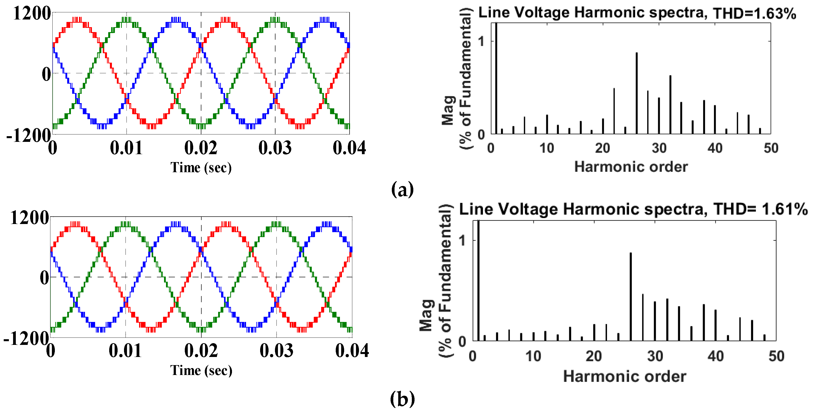
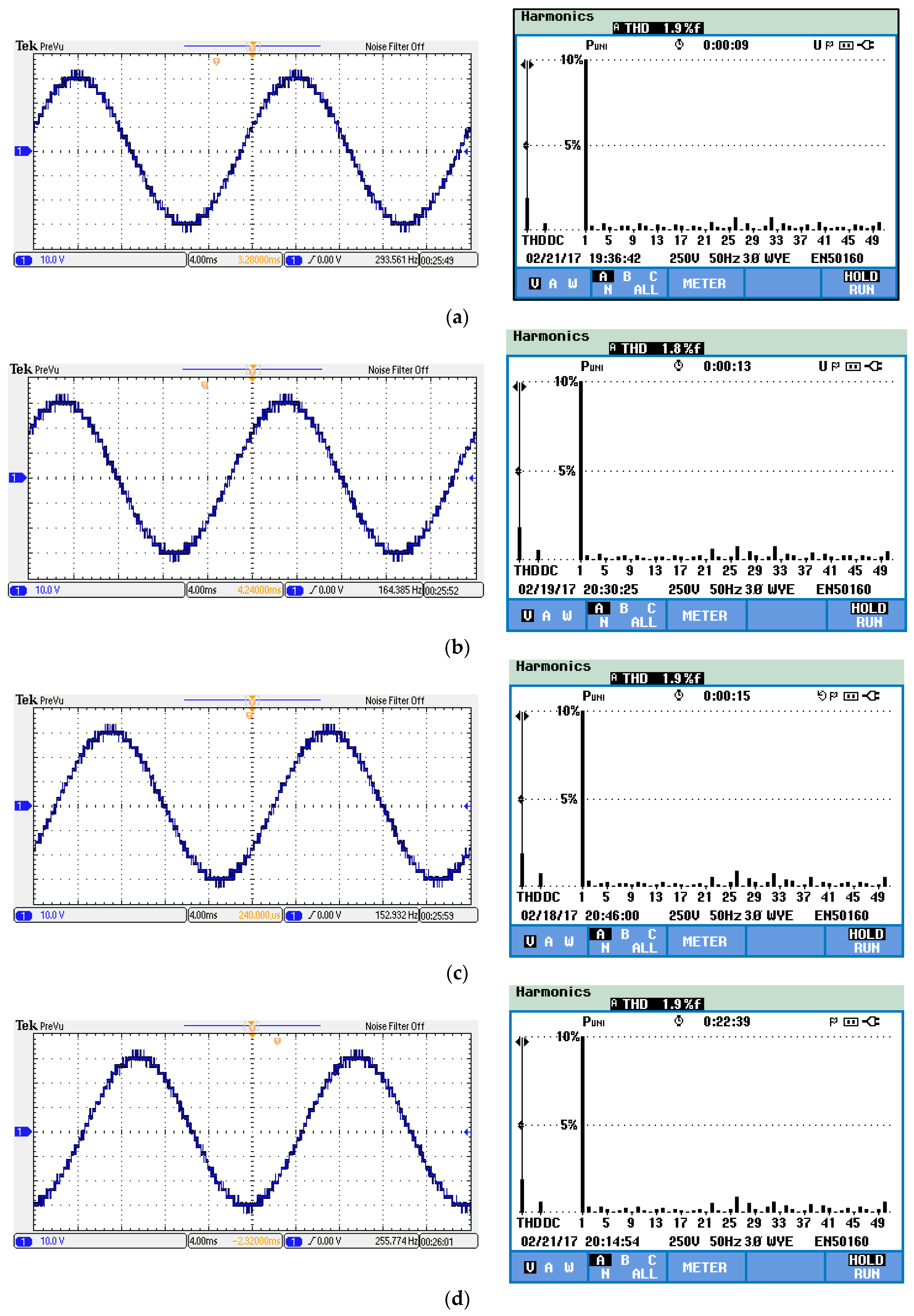
| MLDCL [13] | 1.9% | 1.63% | 2.3% | 2.03% |
| CBSC [15] | 1.8% | 1.61% | 2.3% | 2.13% |
| PUC [14] | 1.9% | 1.61% | 2.3% | 2.13% |
| Hybrid T-type [25,26] | 1.9% | 1.61% | 2.2% | 2.13% |
| E-type [19] | 1.8% | 1.63% | 2.4% | 2.03% |
| CHB [48] | 1.8% | 1.61% | 2.3% | 2.13% |
Disclaimer/Publisher’s Note: The statements, opinions and data contained in all publications are solely those of the individual author(s) and contributor(s) and not of MDPI and/or the editor(s). MDPI and/or the editor(s) disclaim responsibility for any injury to people or property resulting from any ideas, methods, instructions or products referred to in the content. |
© 2023 by the authors. Licensee MDPI, Basel, Switzerland. This article is an open access article distributed under the terms and conditions of the Creative Commons Attribution (CC BY) license (https://creativecommons.org/licenses/by/4.0/).
Share and Cite
Bandela, S.; Sandipamu, T.K.; Vemuganti, H.P.; Rangarajan, S.S.; Collins, E.R.; Senjyu, T. An Efficacious Modulation Gambit Using Fewer Switches in a Multilevel Inverter. Sustainability 2023, 15, 3326. https://doi.org/10.3390/su15043326
Bandela S, Sandipamu TK, Vemuganti HP, Rangarajan SS, Collins ER, Senjyu T. An Efficacious Modulation Gambit Using Fewer Switches in a Multilevel Inverter. Sustainability. 2023; 15(4):3326. https://doi.org/10.3390/su15043326
Chicago/Turabian StyleBandela, Sathyavani, Tara Kalyani Sandipamu, Hari Priya Vemuganti, Shriram S. Rangarajan, E. Randolph Collins, and Tomonobu Senjyu. 2023. "An Efficacious Modulation Gambit Using Fewer Switches in a Multilevel Inverter" Sustainability 15, no. 4: 3326. https://doi.org/10.3390/su15043326
APA StyleBandela, S., Sandipamu, T. K., Vemuganti, H. P., Rangarajan, S. S., Collins, E. R., & Senjyu, T. (2023). An Efficacious Modulation Gambit Using Fewer Switches in a Multilevel Inverter. Sustainability, 15(4), 3326. https://doi.org/10.3390/su15043326