
Analysis and Experimental Validation of Single-Phase Cascaded Boost AC–AC Converter with High Voltage Gain

Abstract
:1. Introduction
- A high-voltage-gain cascaded AC-to-AC boost converter is presented, which utilized low-voltage rating semiconductor devices and multiple cascaded boost units.
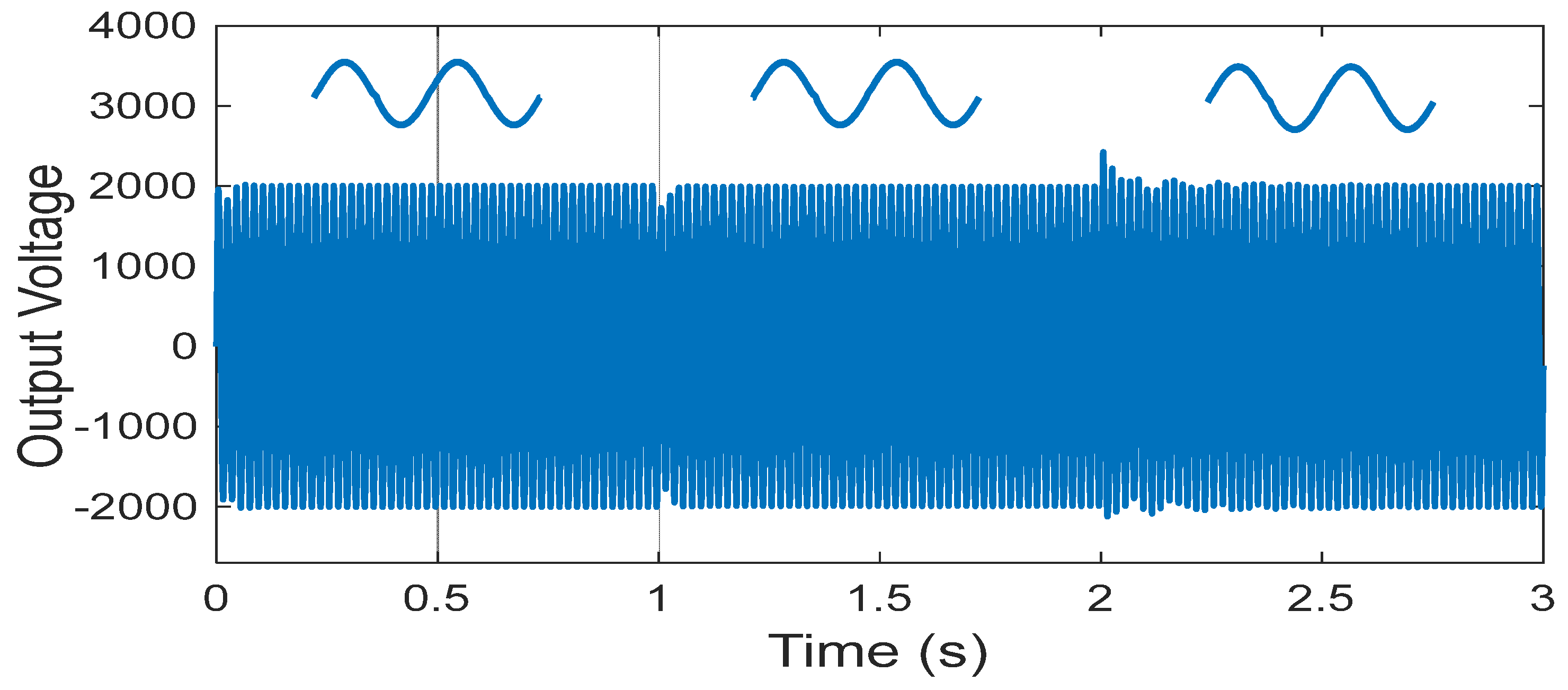
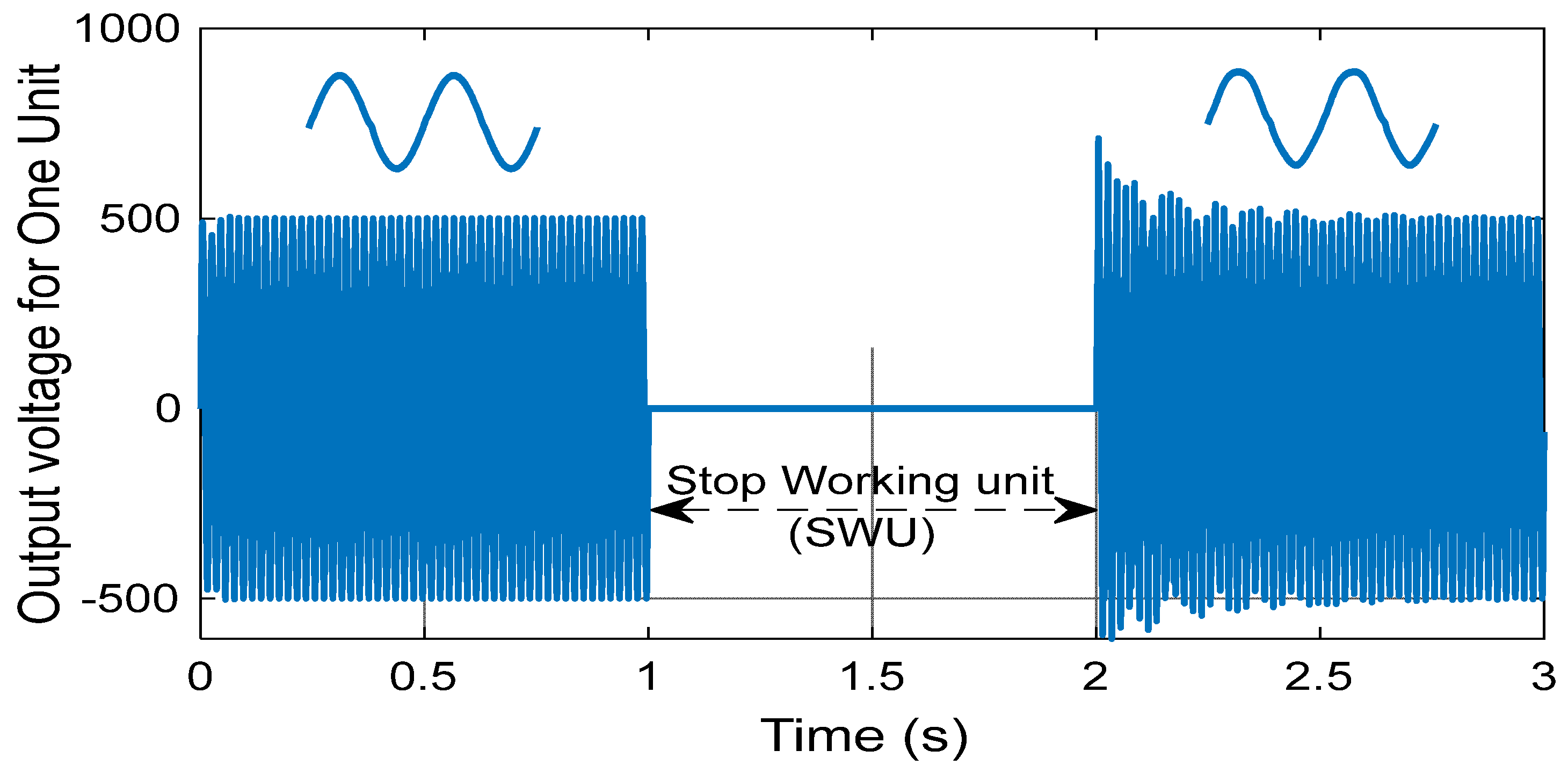
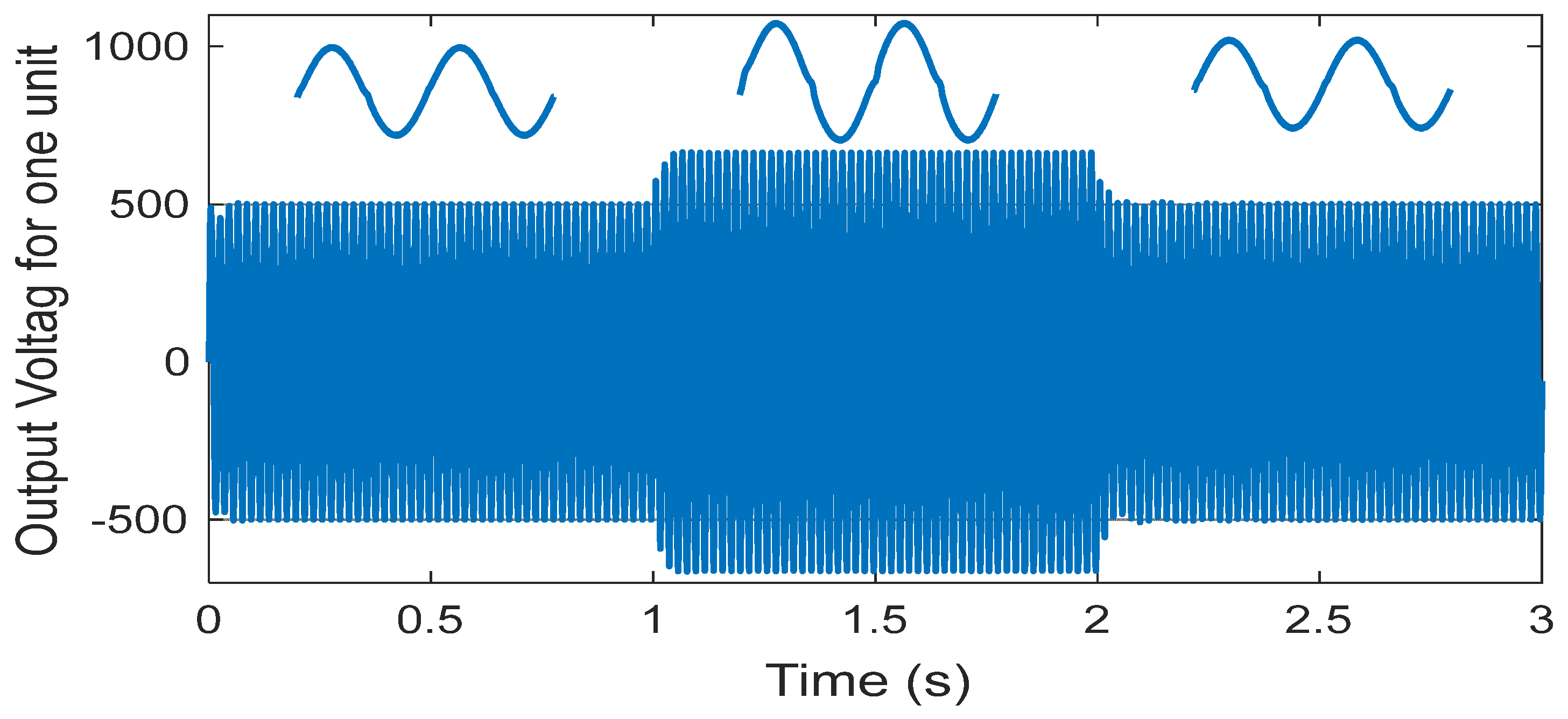
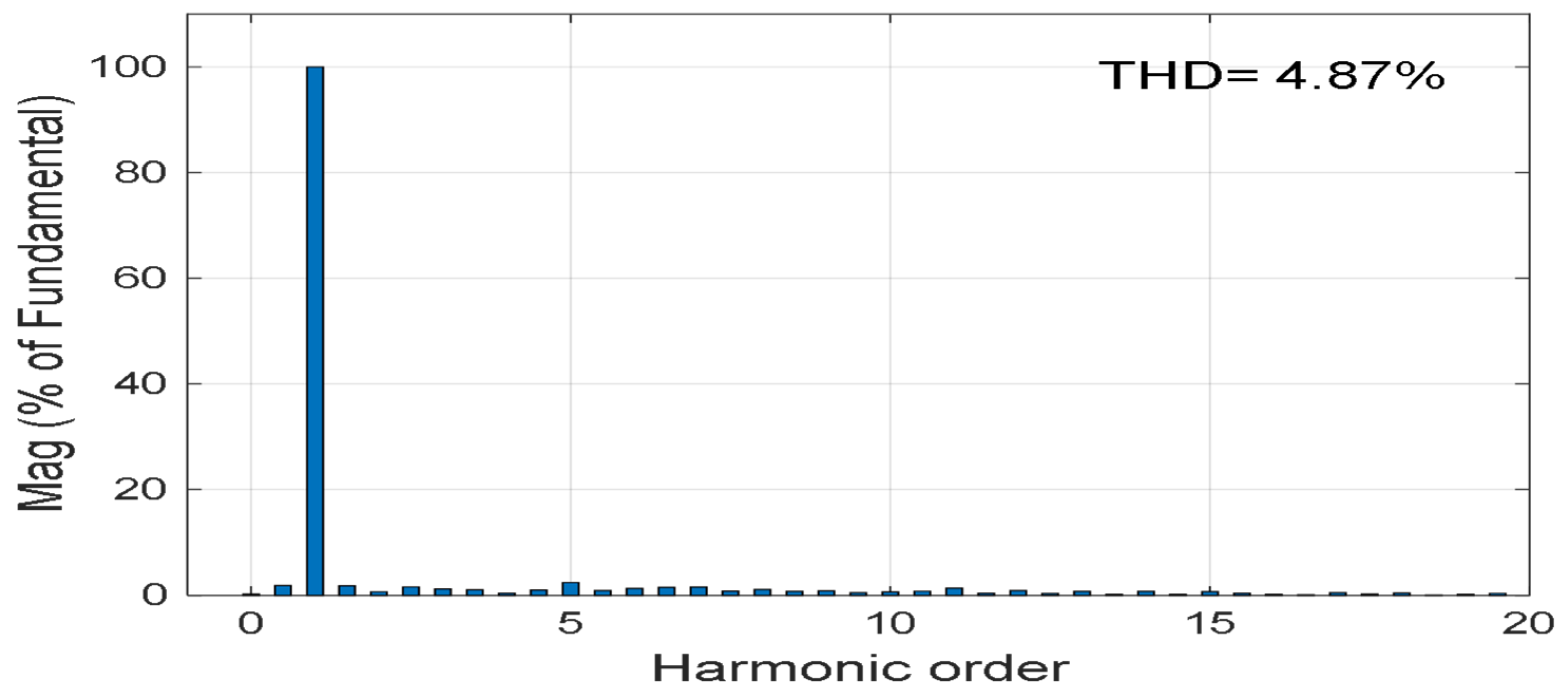
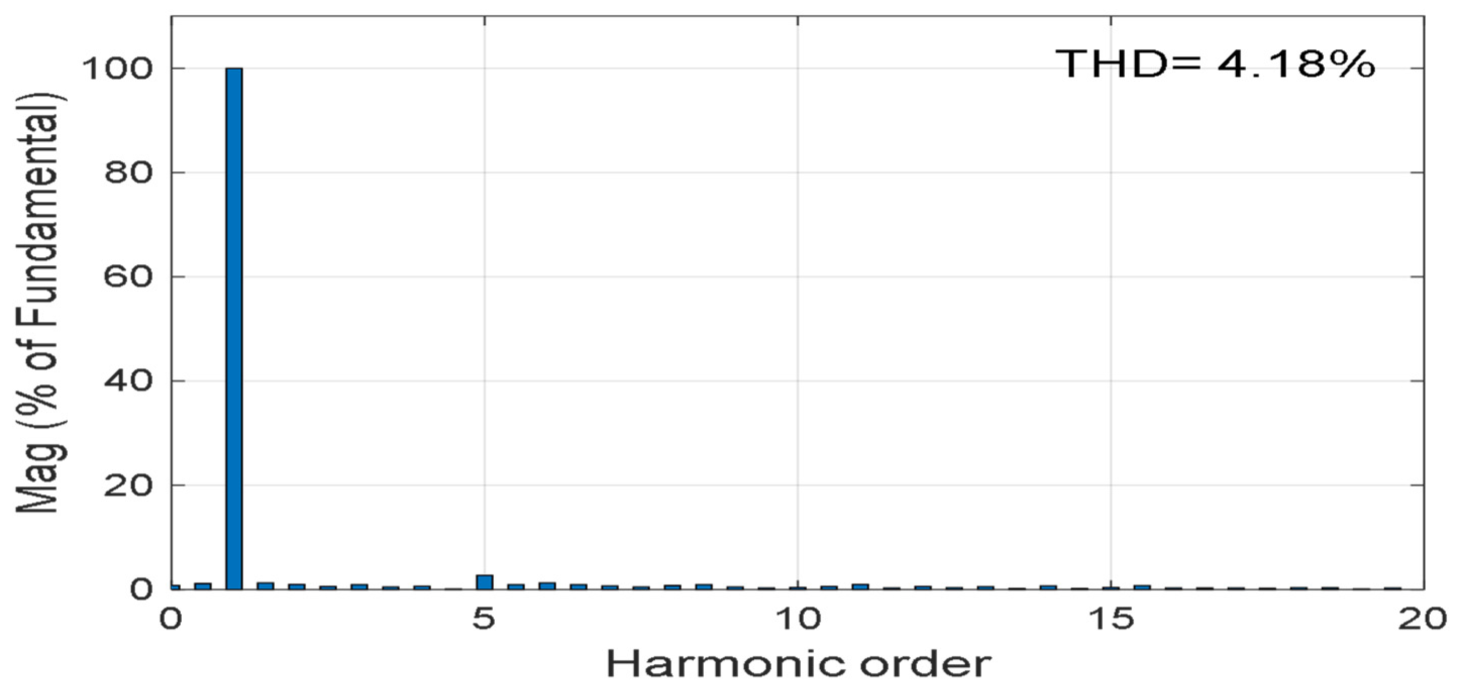
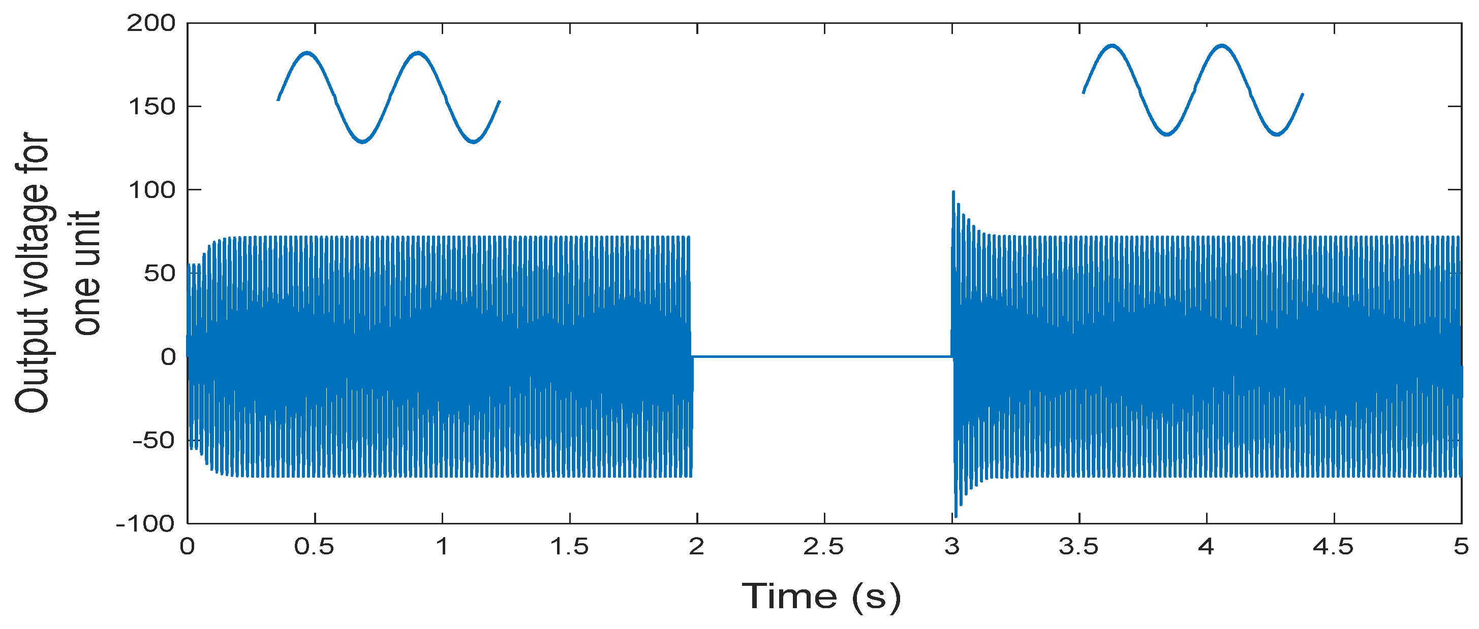
- The output voltage waveform was found to be a sine wave with low harmonics, and the robustness of the control system was confirmed through a case study in which a fault occurred at one unit.
- The control circuit’s ability to maintain the continuity of the output voltage after a fault occurs was confirmed.
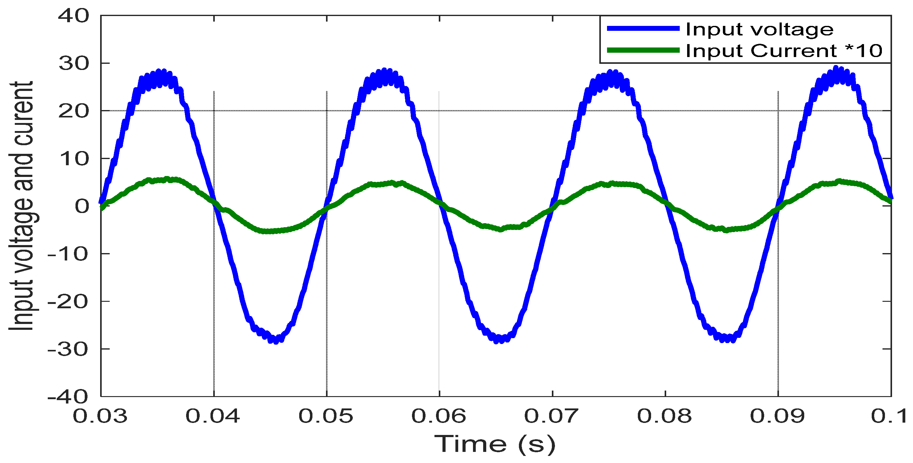
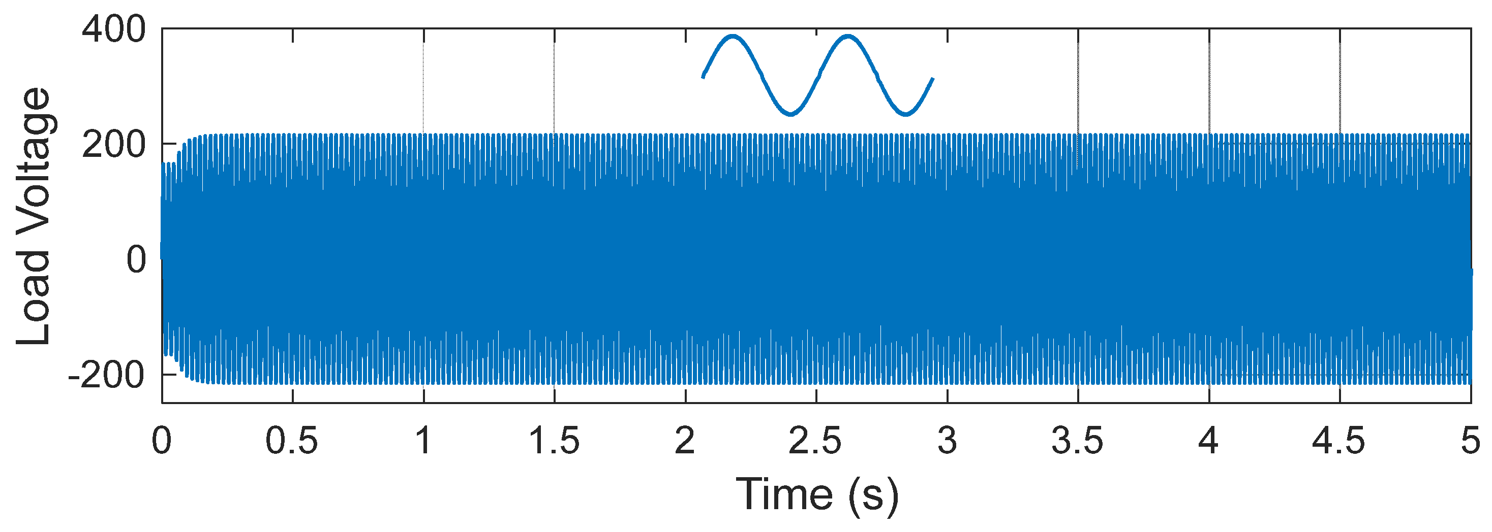
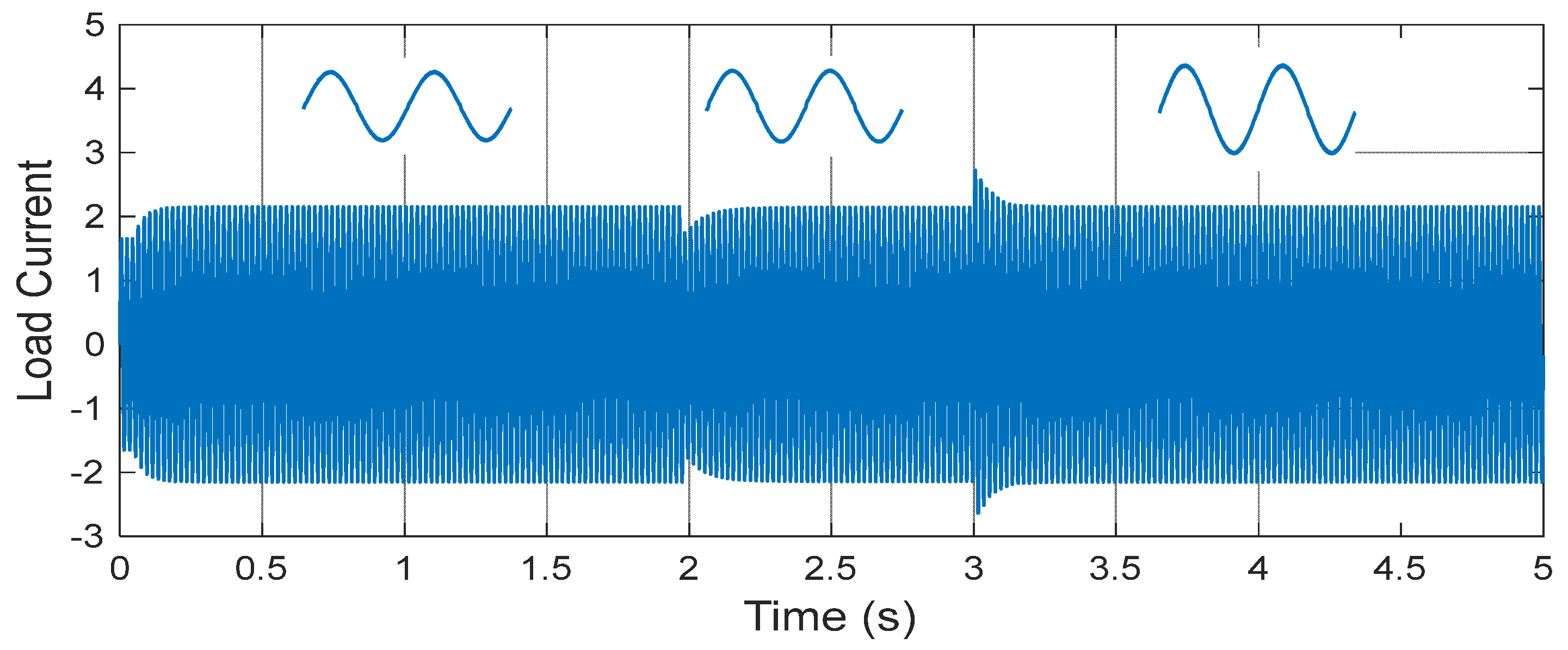
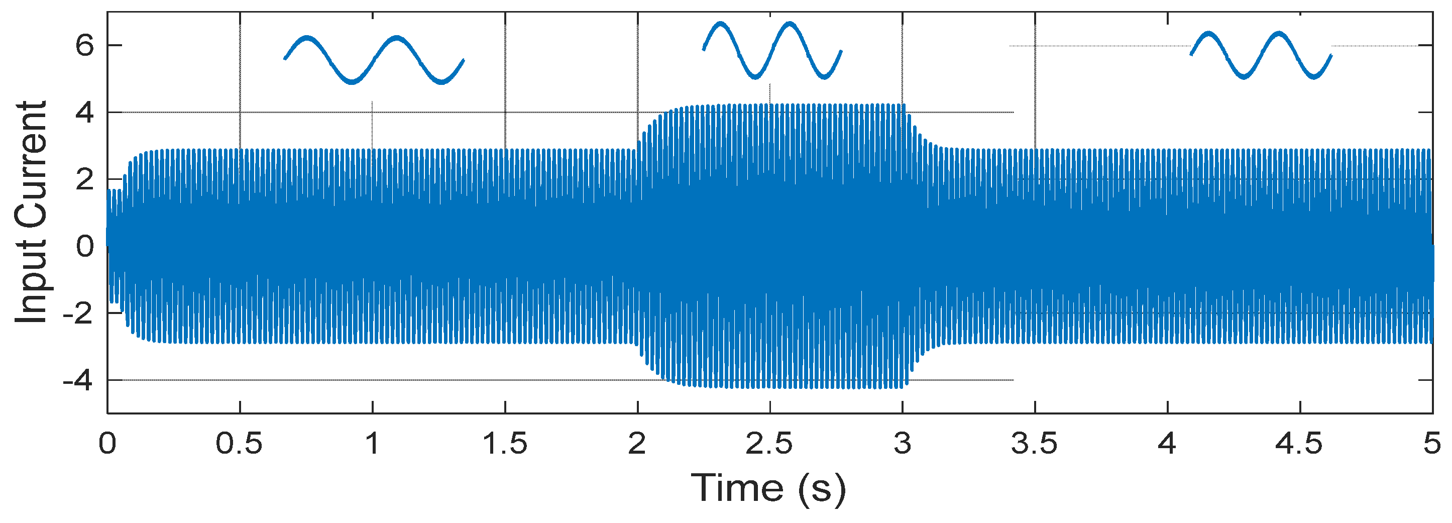
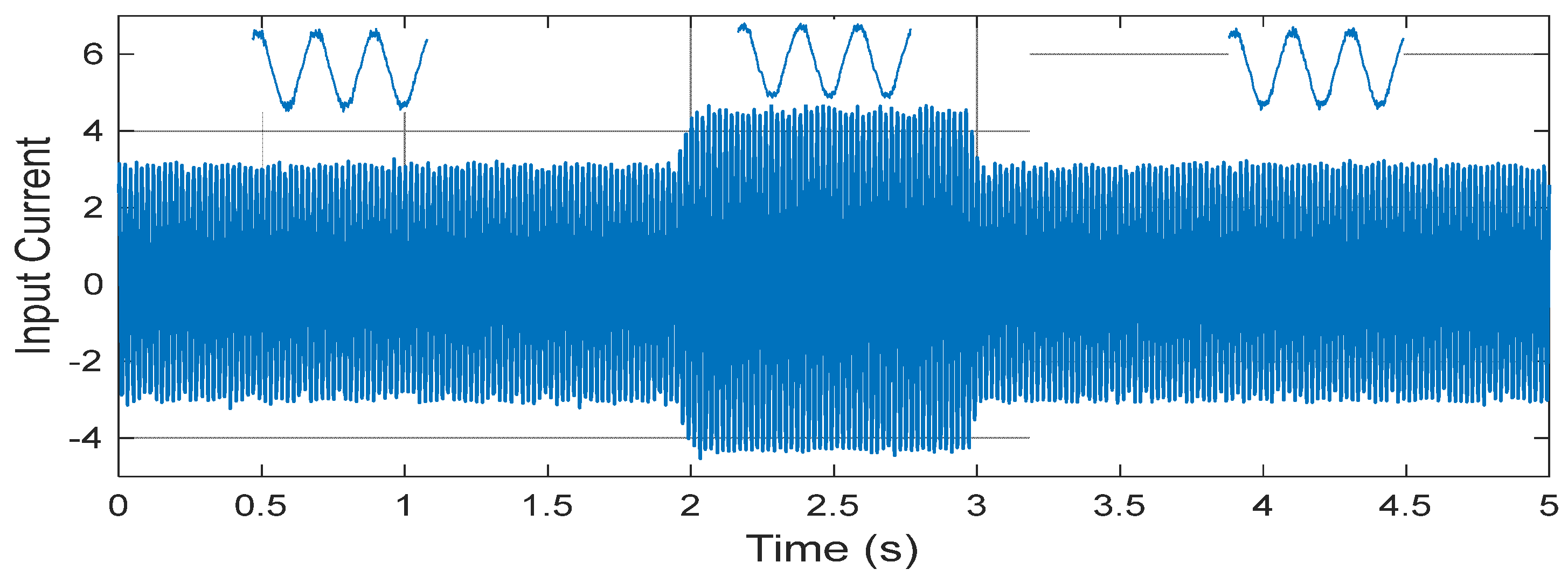
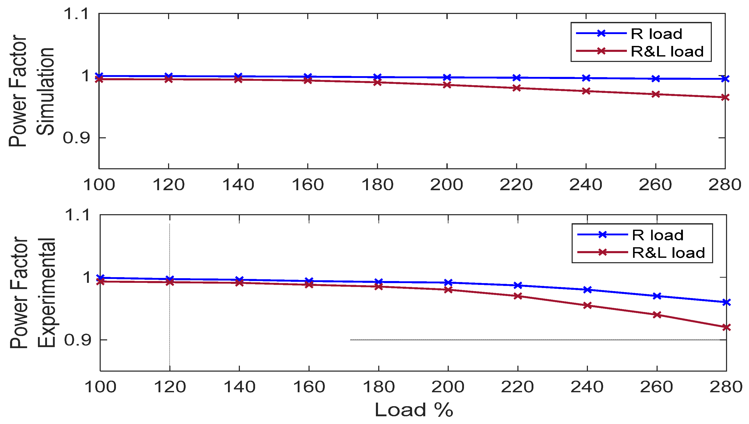
- The proposed circuit was verified through both the simulated and experimental results, which demonstrated an excellent dynamic response with a continuous input current and a power factor close to unity.
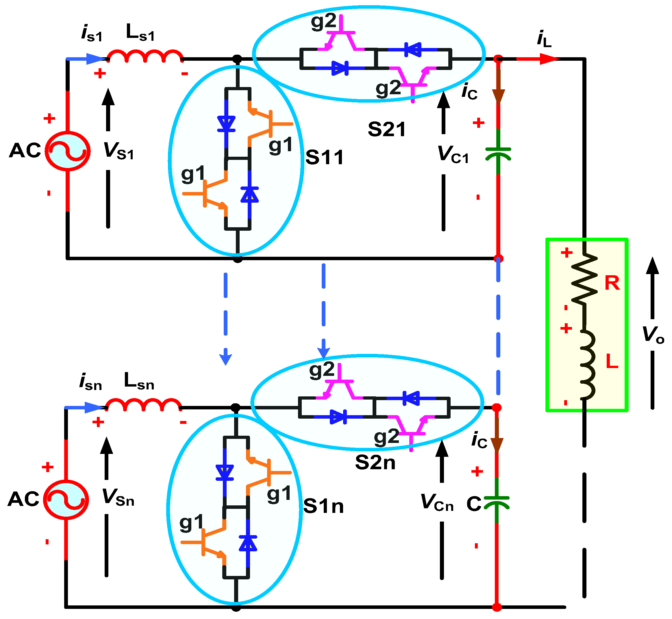
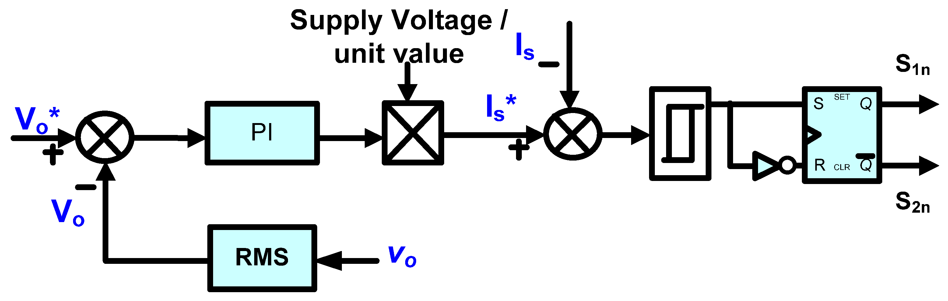
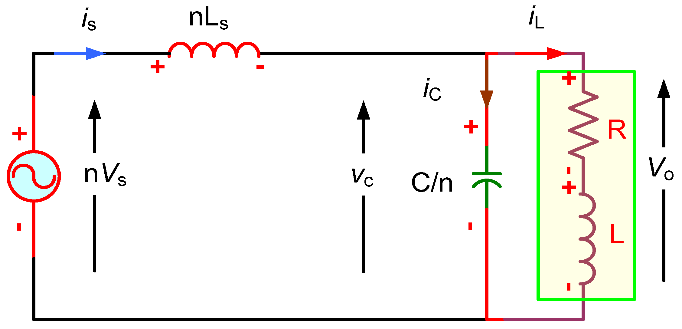
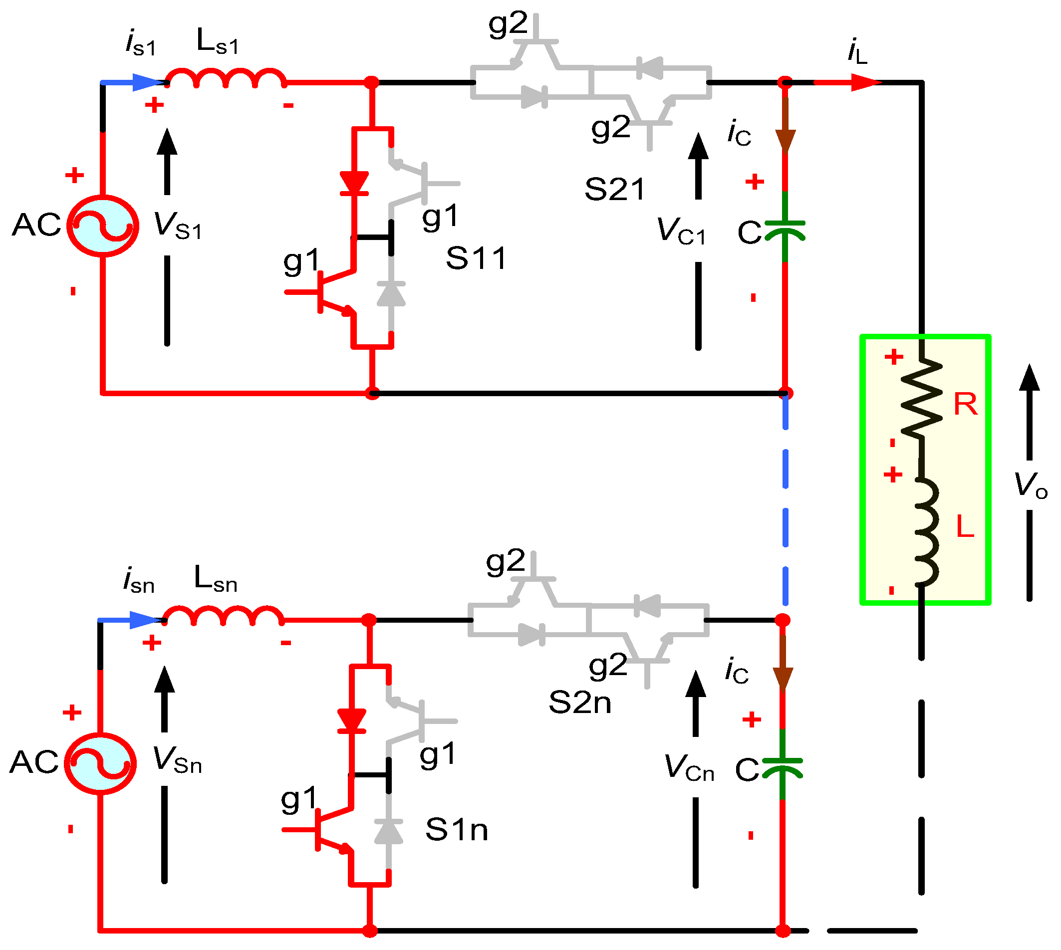
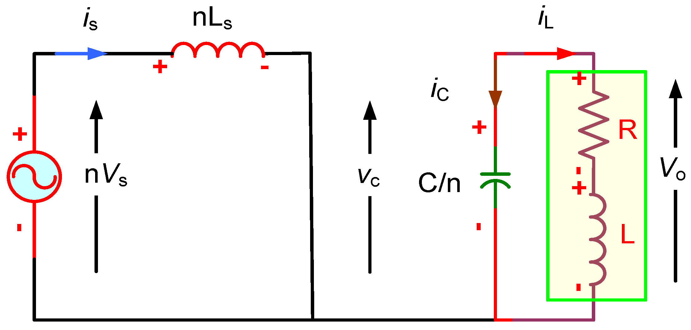
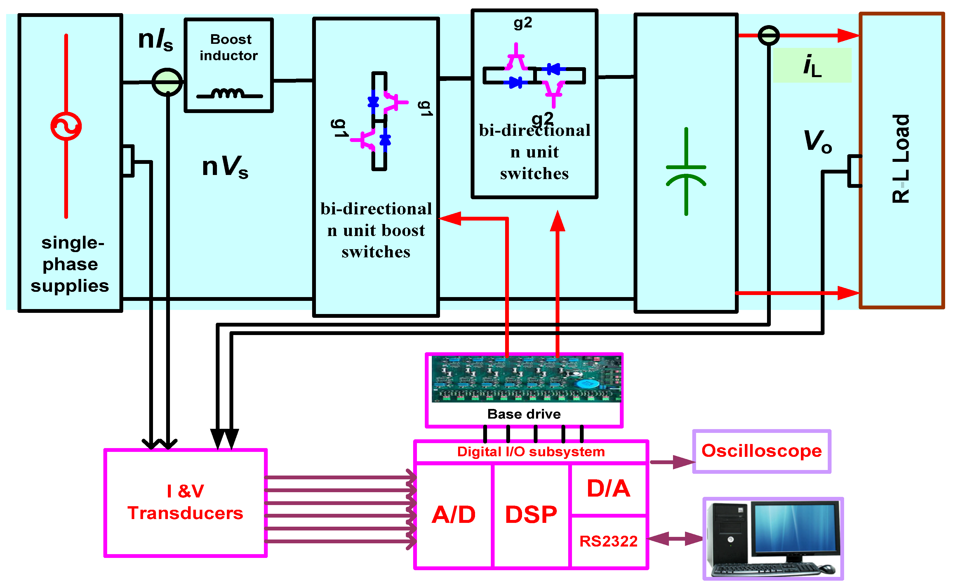
2. Power and Control Circuit
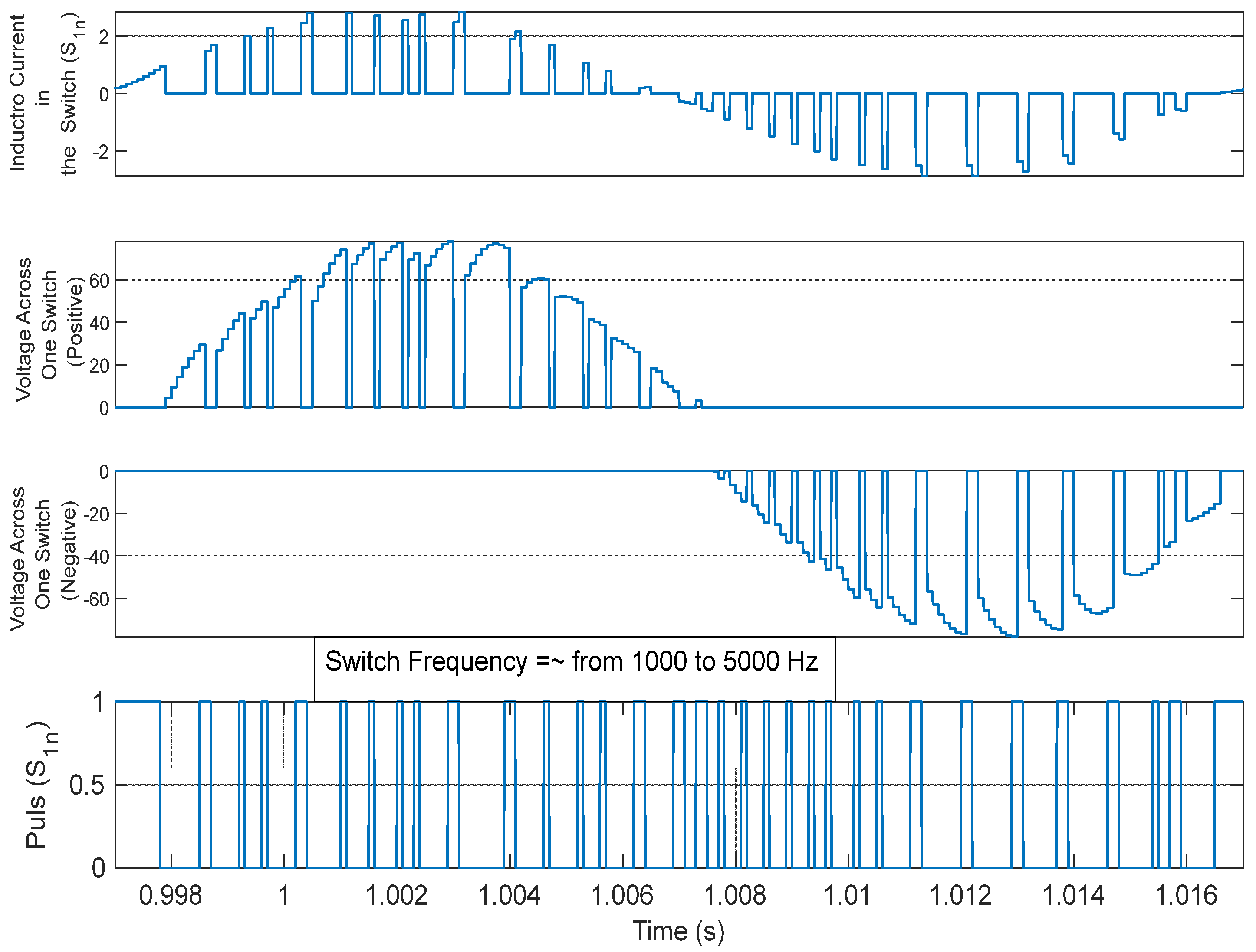
3. Mathematical Analysis and Operation Modes
3.1. Mode 1
3.2. Mode 2
3.3. Average State-Space Representation
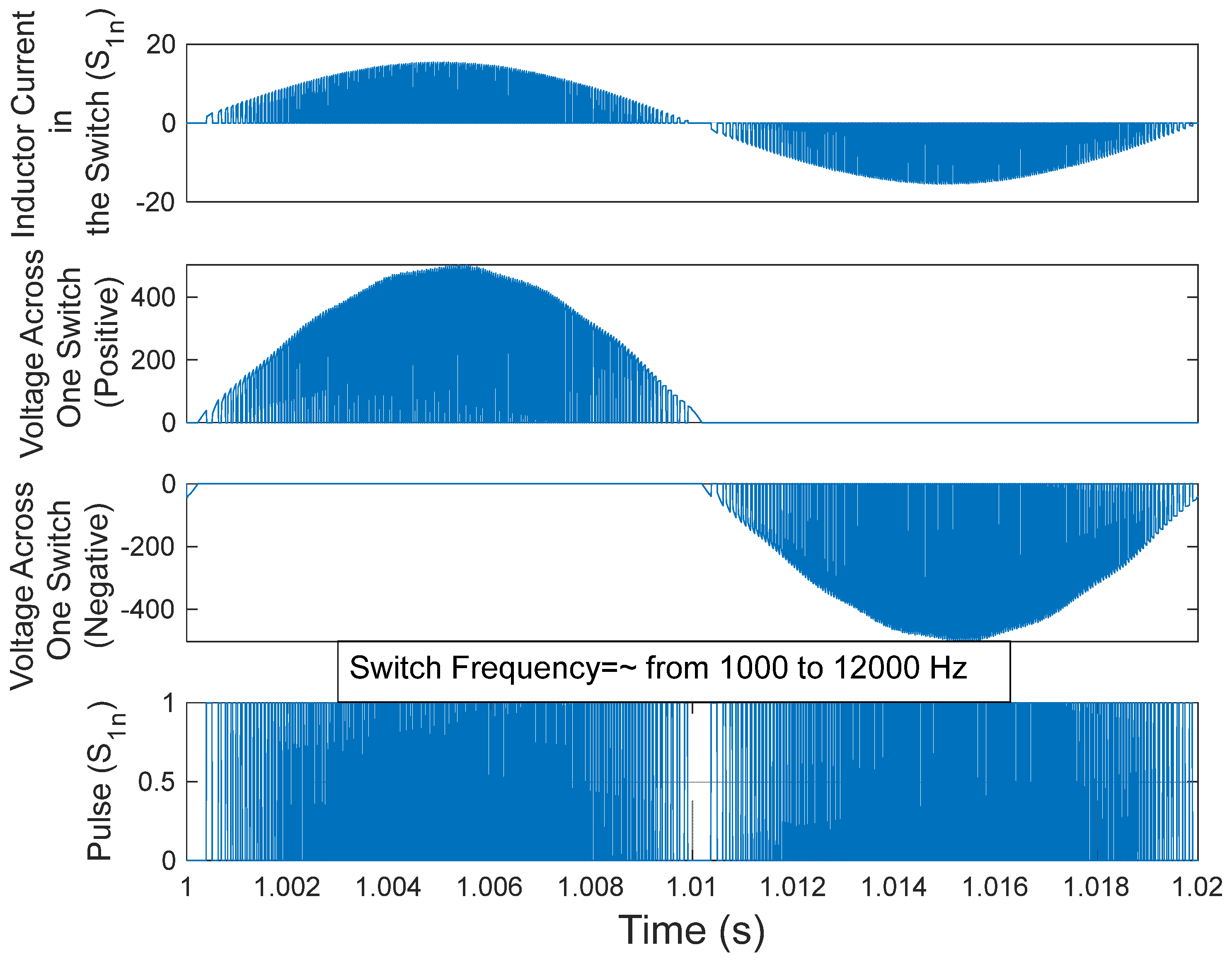
4. Simulated Results
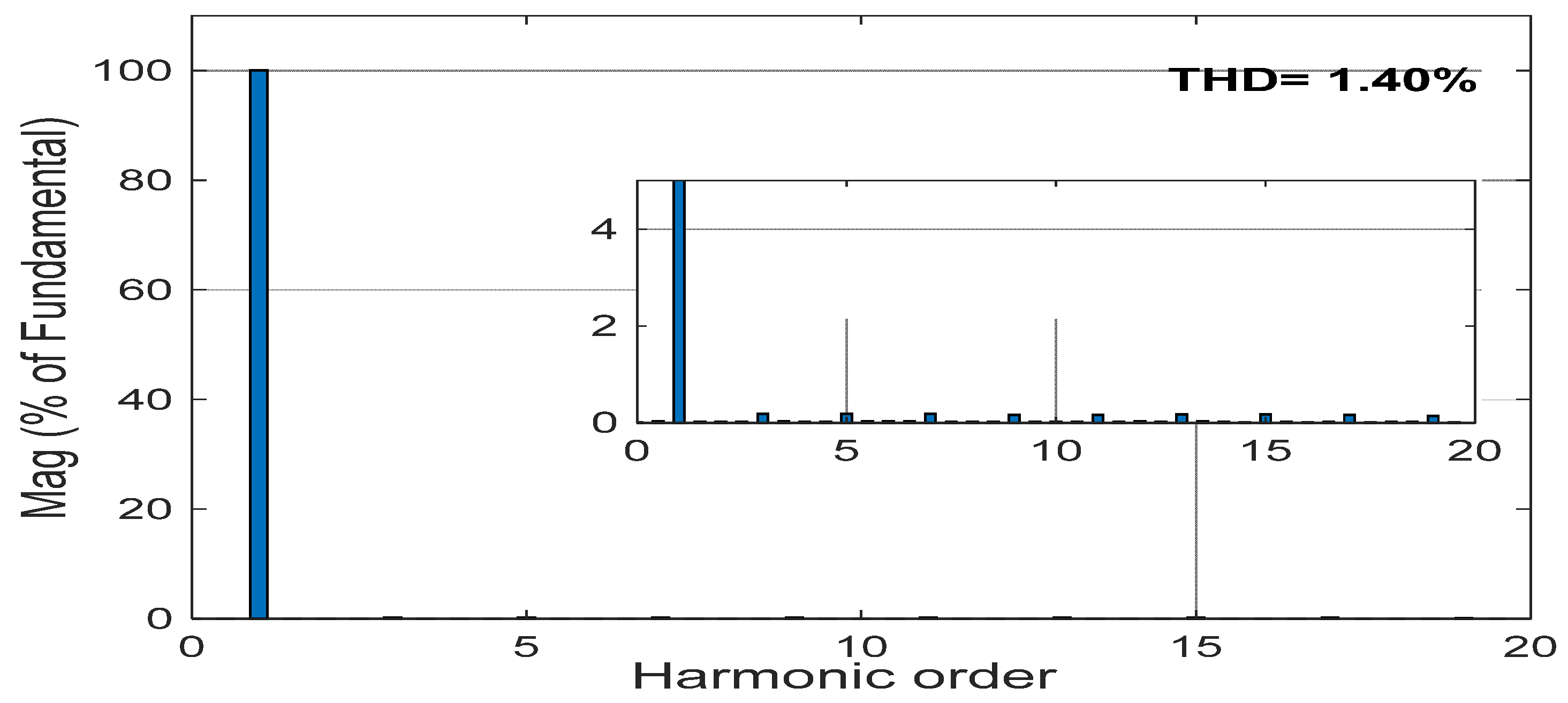
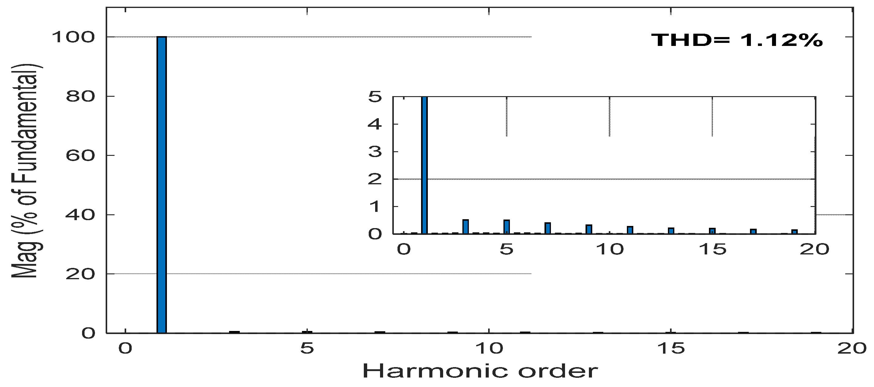
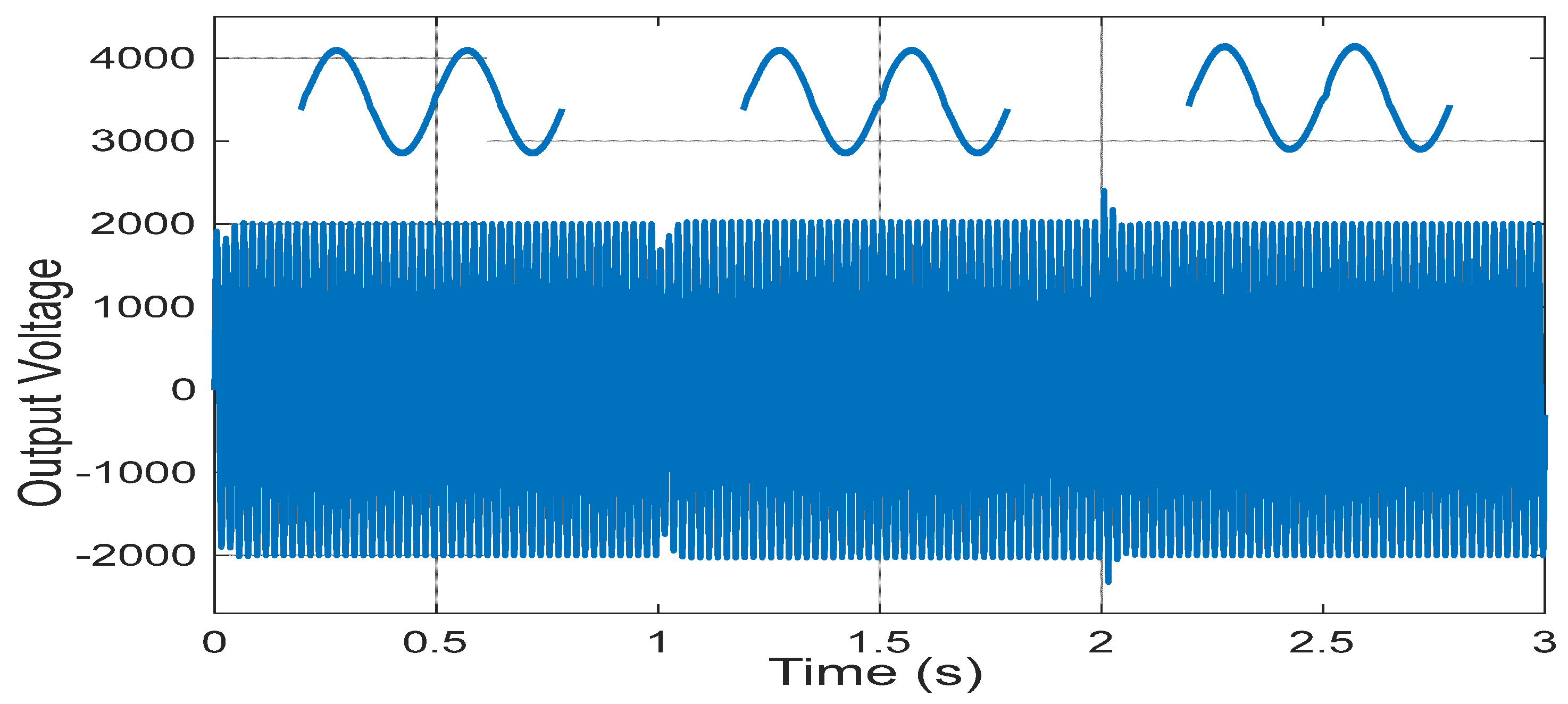
4.1. Steady-State Results Using Four Units
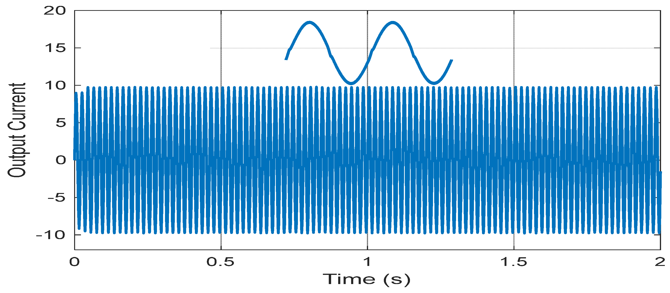
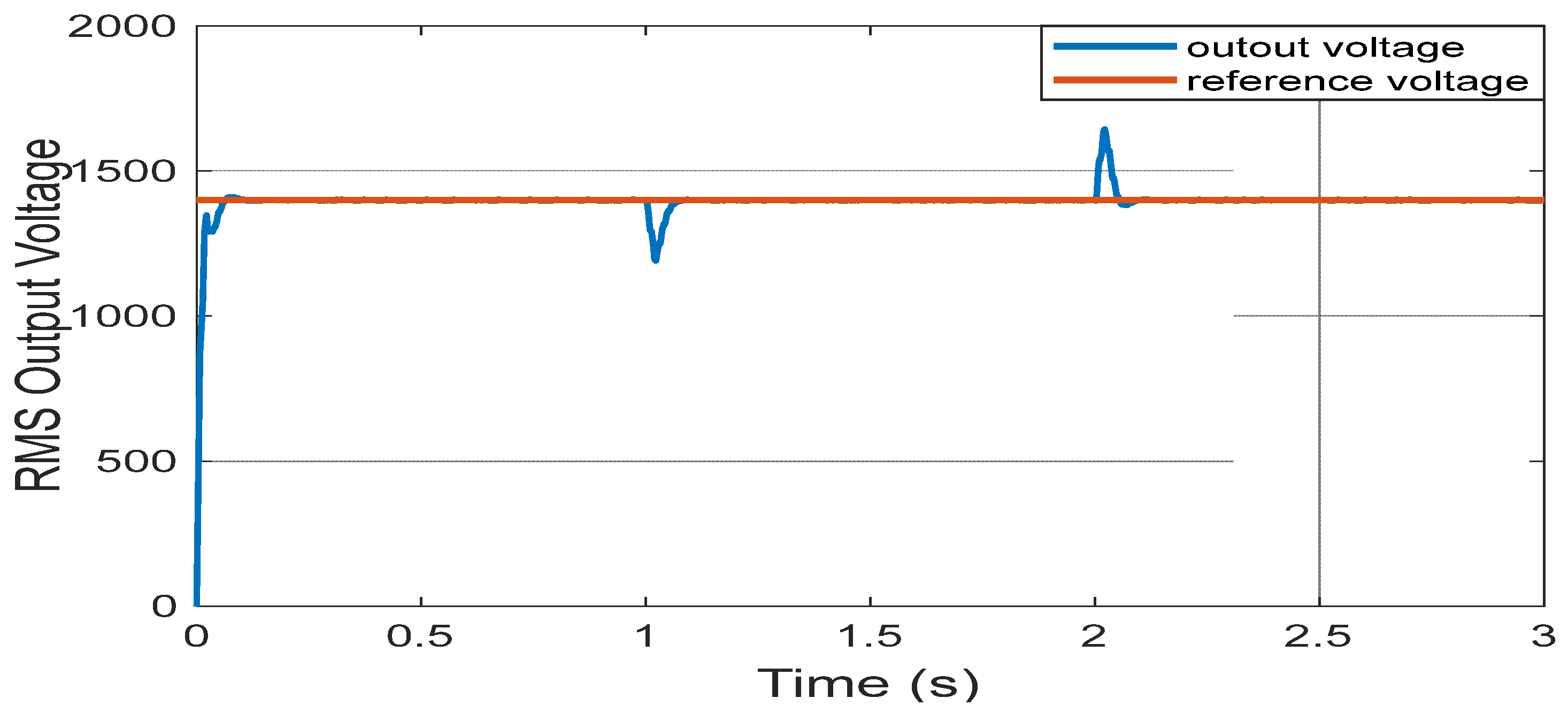
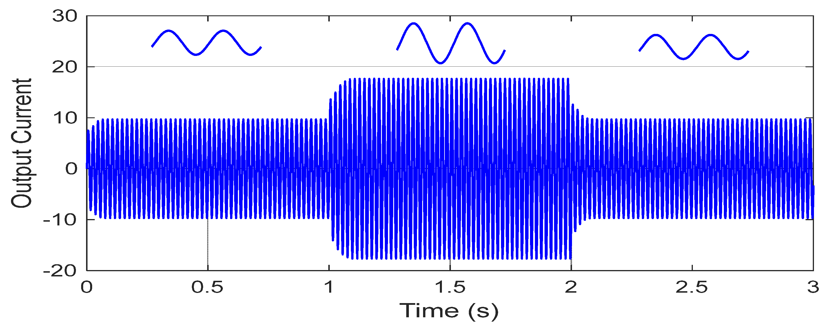
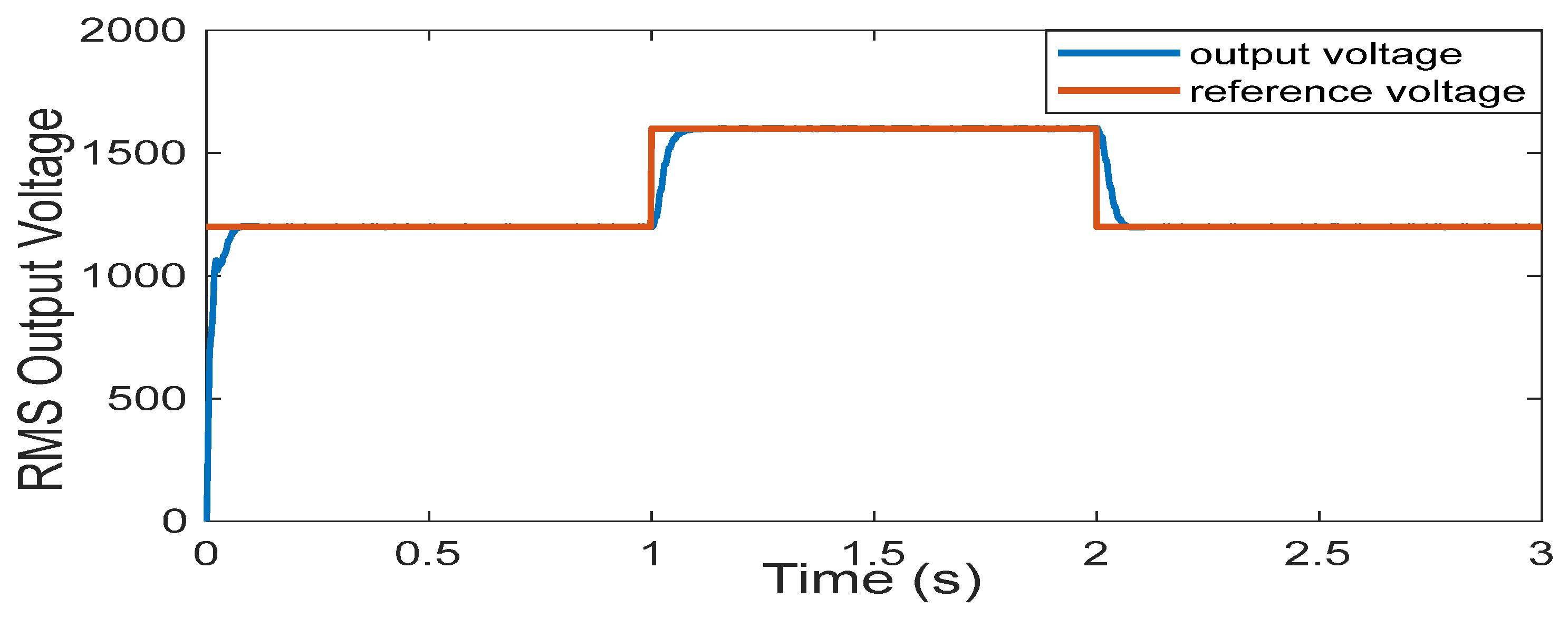
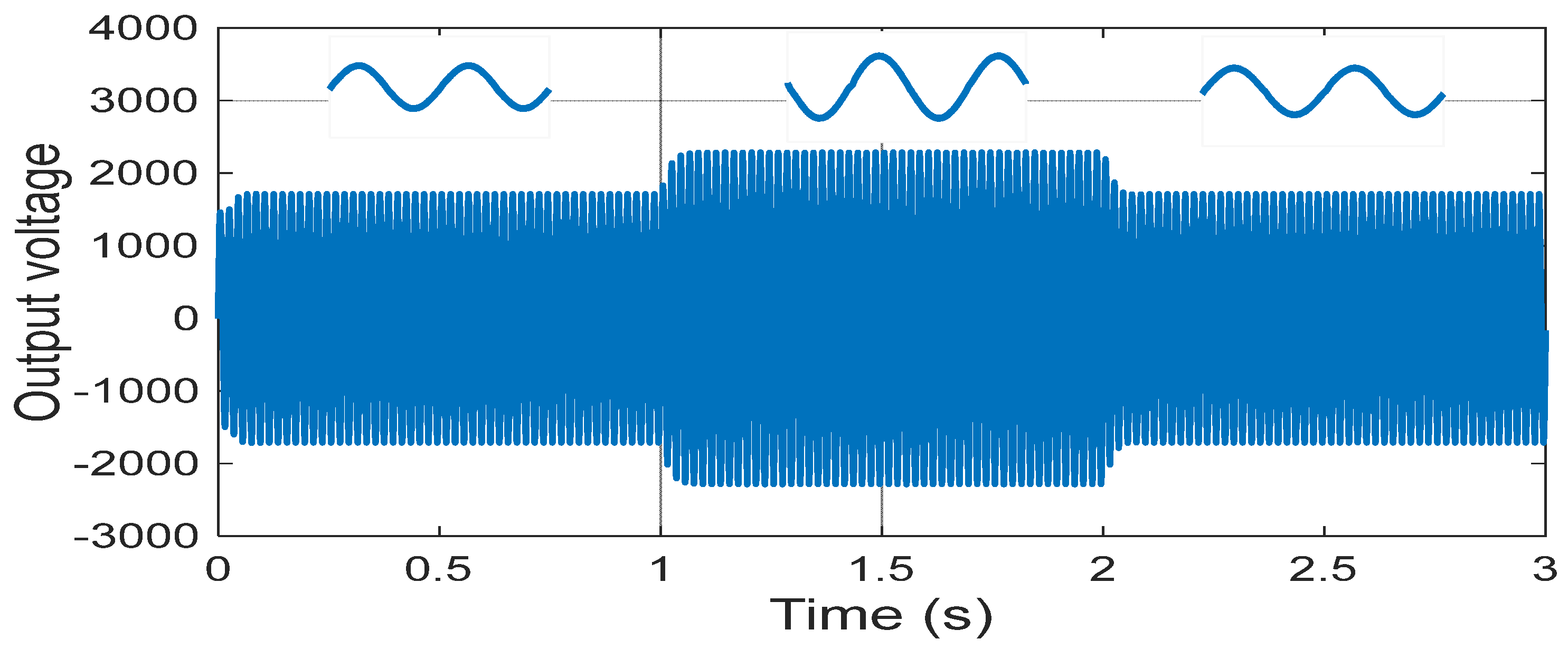
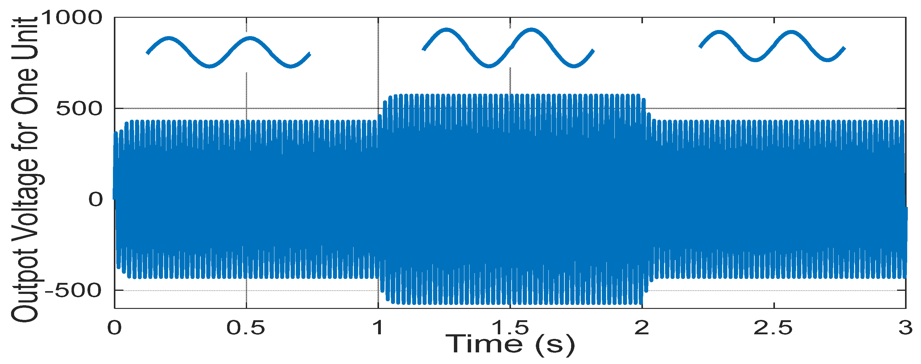
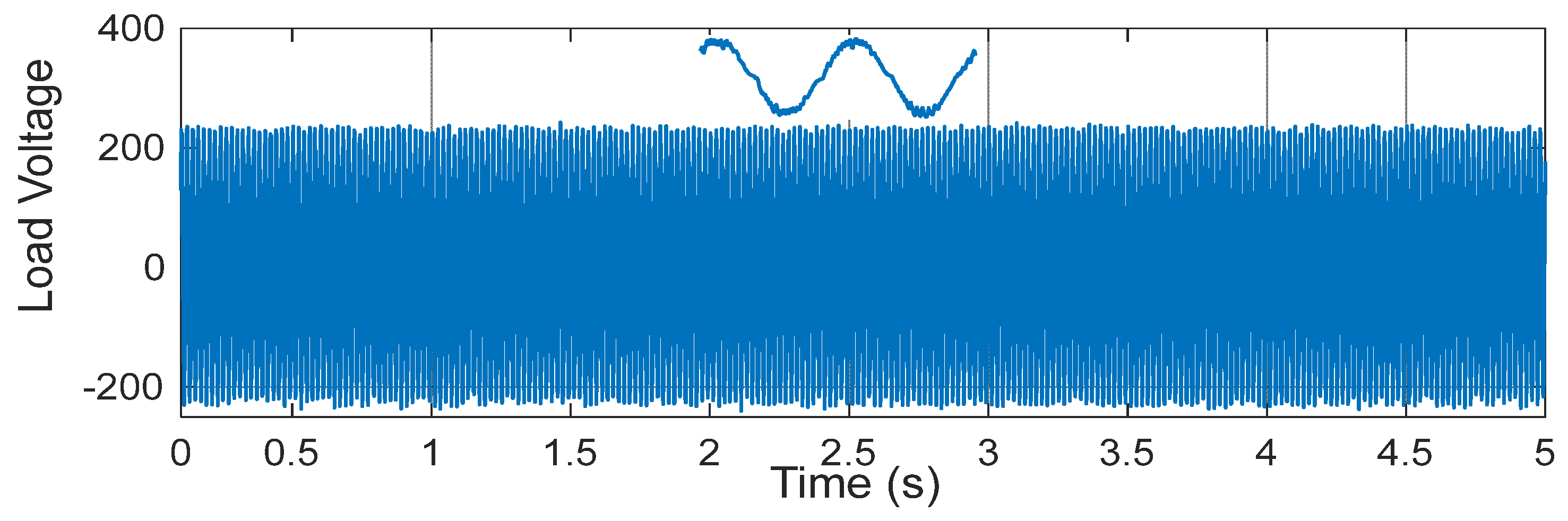
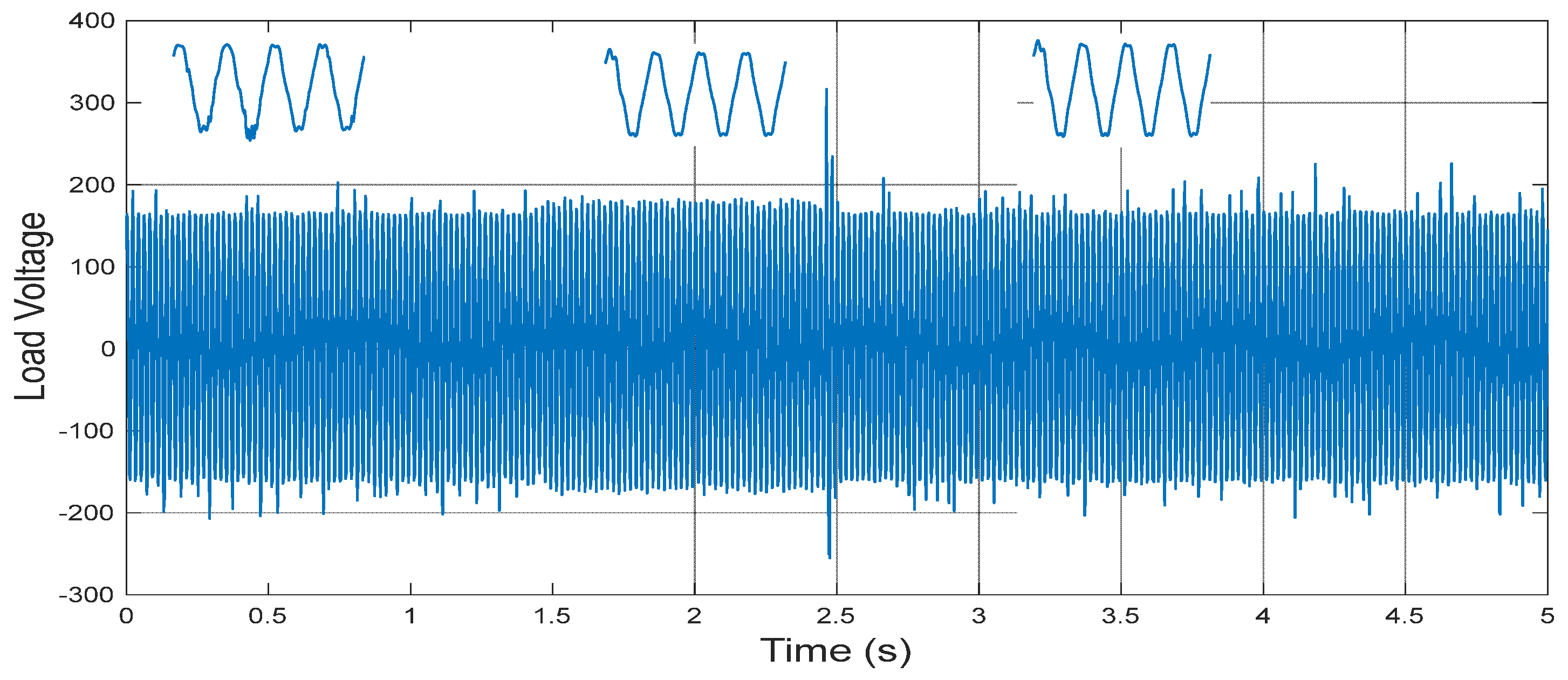
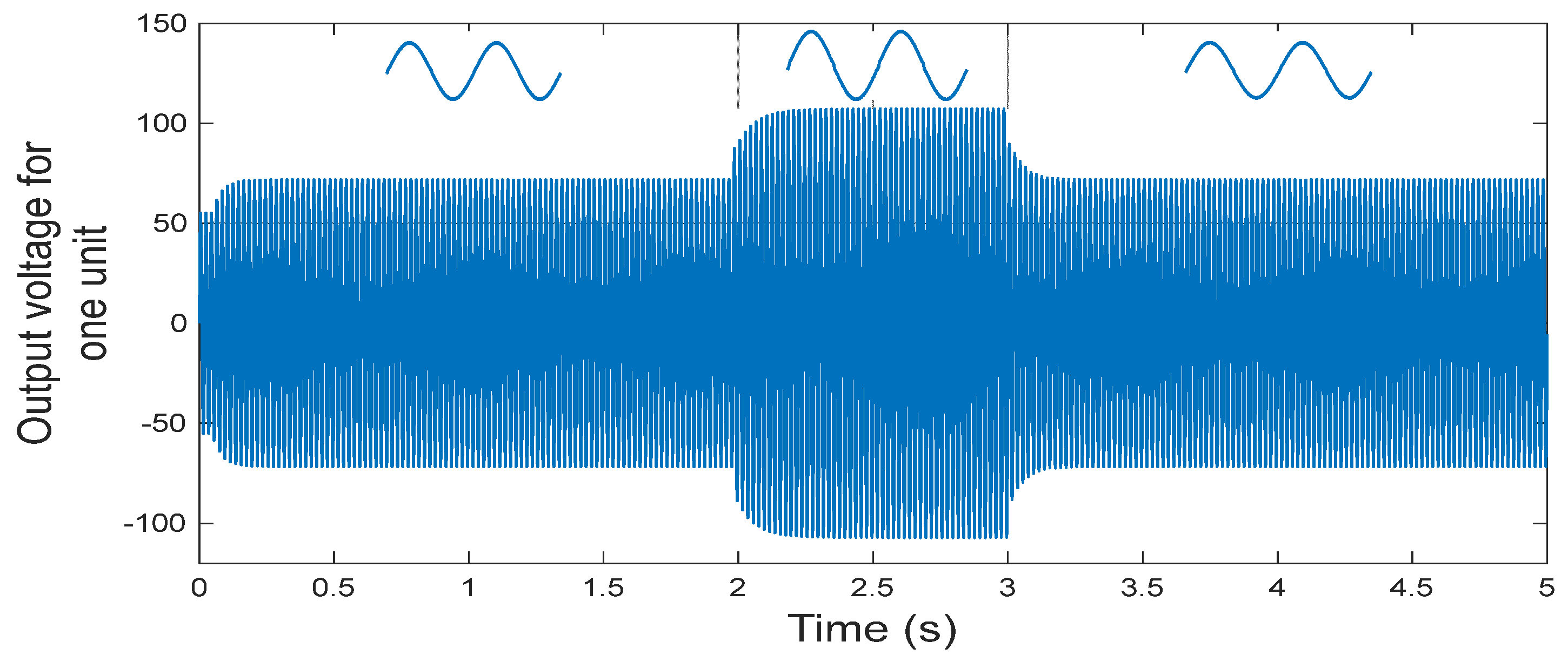
4.2. Transient Results Using Four Units
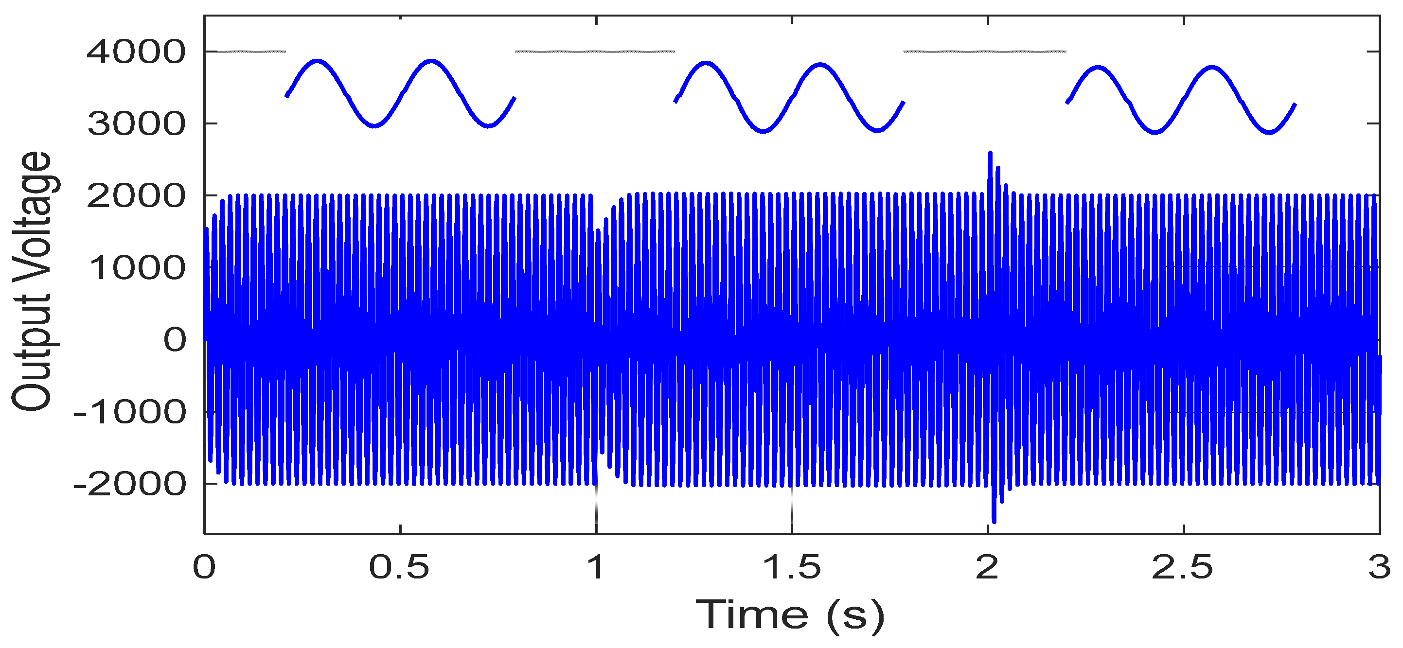
5. Experimental Results
Steady-State Results Using Two Units
6. Comparison between Simulated and Experimental Results Using Three Units
6.1. Steady-State Results Using Three Units
6.2. Transient Results Using Three Units
7. Conclusions
Author Contributions
Funding
Institutional Review Board Statement
Informed Consent Statement
Data Availability Statement
Conflicts of Interest
References
- Liu, C.; Guo, D.; Shan, R.; Cai, G.; Ge, W.; Hu, Z. Novel Bipolar-Type Direct AC–AC Converter Topology Based on Non-Differential AC Choppers. IEEE Trans. Power Electron. 2019, 34, 9585–9599. [Google Scholar] [CrossRef]
- Kaniewski, J.; Szczesniak, P.; Jarnut, M.; Benysek, G. Hybrid Voltage Sag\/Swell Compensators: A Review of Hybrid AC\/AC Converters. IEEE Ind. Electron. Mag. 2015, 9, 37–48. [Google Scholar] [CrossRef]
- Radwan, T.S.; Lashine, A.E.; Rahman, M.A. A novel ac-ac buck-boost voltage regulator with unity input power factor. Int. J. Electron. 2010, 87, 199–210. [Google Scholar] [CrossRef]
- da Silva Filho, O.C.; Tofoli, F.L.; Barreto, L.H.S.C.; de Souza Oliveira, D. Single-Phase Isolated AC–AC Symmetrical Full-Bridge Converter. IEEE J. Emerg. Sel. Top. Power Electron. 2022, 10, 846–855. [Google Scholar] [CrossRef]
- Banerjee, P.K.; Raahemifar, K. AC-AC Voltage Regulation by Switch mode PWM Voltage Controller with Improved performance. Int. J. Eng. Res. Technol. 2013, 2, 2613–2619. [Google Scholar]
- Zahra, S.; Hussainet, J.; Akram, M.M.; Siddique, M. A single-stage AC-DC-AC buck-boost converter with variable frequency operations for power quality. Int. J. Electron. Lett. 2021, 9, 355–369. [Google Scholar] [CrossRef]
- Lee, D.; Kim, Y. Control of Single-Phase-to-Three-Phase AC/DC/AC PWM Converters for Induction Motor Drives. IEEE Trans. Ind. Electron. 2007, 54, 797–804. [Google Scholar] [CrossRef]
- da Silva Filho, O.C.; de Almeida, B.R.; de Souza Oliveira Júnior, D.; Neto, T.R.F. High-Frequency Isolated AC–DC–AC Interleaved Converter for Power Quality Applications. IEEE Trans. Ind. Appl. 2018, 54, 4594–4602. [Google Scholar] [CrossRef]
- Wang, Y.; Wang, P.; Cai, G.; Liu, C.; Guo, D.; Zh, H. An Improved Bipolar-Type AC–AC Converter Topology Based on Nondifferential Dual-Buck PWM AC Choppers. IEEE Trans. Power Electron. 2021, 36, 4052–4065. [Google Scholar] [CrossRef]
- Wen, B.; Zhang, X.; Wang, Q.; Burgos, R.; Mattavelli, P.; Boroyevich, D. Comparison of three-phase ac-ac matrix converter and voltage dc-link back-to-back converter topologies based on EMI filter. In Proceedings of the 2013 IEEE Energy Conversion Congress and Exposition, Denver, CO, USA, 15–19 September 2013; pp. 2698–2706. [Google Scholar] [CrossRef]
- Ellabban, O.; Abu-Rub, H.; Bayhan, S. Z-Source Matrix Converter: An Overview. IEEE Trans. Power Electron. 2016, 31, 7436–7450. [Google Scholar] [CrossRef]
- Sun, Y.; Li, X.; Su, M.; Wang, H.; Dan, H.; Xiong, W. Indirect Matrix Converter-Based Topology and Modulation Schemes for Enhancing Input Reactive Power Capability. IEEE Trans. Power Electron. 2015, 30, 4669–4681. [Google Scholar] [CrossRef]
- Nguyen, T.D.; Lee, H.-H. Dual Three-Phase Indirect Matrix Converter with Carrier-Based PWM Method. IEEE Trans. Power Electron. 2014, 29, 569–581. [Google Scholar] [CrossRef]
- Sharifi, S.; Monfared, M.; Nikbahar, A. Highly Efficient Single-Phase Direct AC-to-AC Converter with Reduced Semiconductor Count. IEEE Trans. Ind. Electron. 2021, 68, 1130–1138. [Google Scholar] [CrossRef]
- Ashraf, N.; Izhaet, T.; Abbas, G.; Balas, V.E.; Balas, M.M.; Lin, T.; Asad, M.U.; Farooq, U.; Gu, J. A Single-Phase Buck and Boost AC-to-AC Converter with Bipolar Voltage Gain: Analysis, Design, and Implementation. Energies 2019, 12, 1376. [Google Scholar] [CrossRef]
- Kolar, J.W.; Friedli, T.; Rodriguez, J.; Wheeler, P.W. Review of Three-Phase PWM AC–AC Converter Topologies. IEEE Trans. Ind. Electron. 2011, 58, 4988–5006. [Google Scholar] [CrossRef]
- Peng, F.Z.; Chen, L.; Zhang, F. Simple topologies of PWM AC-AC converters. IEEE Power Electron. Lett. 2003, 1, 10–13. [Google Scholar] [CrossRef]
- Ursaru, O.; Lucanu, M.; Aghion, C.; Lucanu, N. Single-Phase Direct Boost AC-AC Converter. Adv. Electr. Comput. Eng. 2017, 17, 43–48. [Google Scholar] [CrossRef]
- Lucanu, M.; Ursaru, O.; Aghion, C.; Lucanu, N. Single-Phase Direct AC-AC Boost Converter. Adv. Electr. Comput. Eng. 2014, 14, 107–112. [Google Scholar] [CrossRef]
- Kabir, M.A.; Abedin, A.H.; Mustafiz, R.B.; Islam, M.K.; Choudhury, M.A. A single phase AC-AC boost converter with improved input power factor and THD. In Proceedings of the International Aegean Conference on Electrical Machines and Power Electronics and Electromotion, Joint Conference, Istanbul, Turkey, 8–10 September 2011; pp. 764–767. [Google Scholar] [CrossRef]
- Khan, U.A.; Lee, J.; Park, J.-W. An Improved Cascaded Dual-Buck AC-AC Converter. In Proceedings of the 2020 IEEE 9th International Power Electronics and Motion Control Conference (IPEMC2020-ECCE Asia), Nanjing, China, 29 November–2 December 2020; pp. 1248–1253. [Google Scholar] [CrossRef]
- Li, L.; Tang, D. Cascade Three-Level AC/AC Direct Converter. IEEE Trans. Ind. Electron. 2012, 59, 27–34. [Google Scholar] [CrossRef]
- Kim, S.; Kim, H.-G.; Cha, H. A novel single-phase cascaded multilevel AC-AC converter without commutation problem. In Proceedings of the 2014 IEEE Energy Conversion Congress and Exposition (ECCE), Pittsburgh, PA, USA, 14–18 September 2014; pp. 556–562. [Google Scholar] [CrossRef]
- Khan, A.A.; Cha, H.; Baek, J.; Kim, J.; Cho, J. Cascaded Dual-Buck AC–AC Converter with Reduced Number of Inductors. IEEE Trans. Power Electron. 2017, 32, 7509–7520. [Google Scholar] [CrossRef]
- Ahmed, H.F.; El Moursi, M.S.; Zahawi, B.; Al Hosani, K. A High-Frequency Isolated Multilevel Cascaded-Type Bipolar Direct PWM AC–AC Converter for Utility Voltage Compensation. IEEE Trans. Ind. Appl. 2021, 57, 3188–3201. [Google Scholar] [CrossRef]
- Ahmed, H.; Çelik, D. Sliding mode based adaptive linear neuron proportional resonant control of Vienna rectifier for performance improvement of electric vehicle charging system. J. Power Sources 2022, 542, 231788. [Google Scholar] [CrossRef]
- Middlebrook, R.D.; Cuk, S. A general unified approach to modelling switching-converter power stages. In Proceedings of the 1976 IEEE Power Electronics Specialists Conference, Cleveland, OH, USA, 8–10 June 1976; pp. 18–34. [Google Scholar] [CrossRef]
- Sun, J.; Grotstollen, H. Averaged modelling of switching power converters: Reformulation and theoretical basis. In Proceedings of the PESC’92 Record. 23rd Annual IEEE Power Electronics Specialists Conference, Toledo, Spain, 29 June–3 July 1992; Volume 2, pp. 1165–1172. [Google Scholar] [CrossRef]
- Sun, J.; Grotstollen, H. Symbolic analysis methods for averaged modeling of switching power converters. IEEE Trans. Power Electron. 1997, 12, 537–546. [Google Scholar] [CrossRef]
- Lashine, A.E.; Osheba, M.S.; Mansour, A.S. Stability Analysis and Performance Evaluation of a Multifunction Converter. Eng. Res. J. 2021, 44, 125–134. [Google Scholar] [CrossRef]


| Parameter | Symbol | Value |
|---|---|---|
| Supply phase voltage | = = | 220 V |
| System frequency | 50 Hz | |
| Coil inductance | 15 mH | |
| Capacitor | 15 µF | |
| Load resistance | 200 Ω | |
| Load inductance | 200 mH |
| Topology | No. of Units | Inductors | Coupled Inductors | Capacitors | Switches | Diodes | Total Components | Voltage Gain (Vo/Vin) | Output Voltage Gain | Function Unit |
|---|---|---|---|---|---|---|---|---|---|---|
| 24 | 2 | 2 | 2 | 4 | 8 | 8 | 24 | 2D | 1 * Vin | buck |
| 25 | 3 | - | - | 2 | 12 | 12 | 26 | (D + D’)/(2(1 − D)) | 1 * Vin | buck |
| 26 | 4 | 1 | 8 | 8 | 16 | 16 | 49 | 4D | 2 * Vin | buck |
| 27 | 4 | 1 | 8 | 9 | 16 | 16 | 50 | n * D | 2 * Vin | buck |
| Proposed | 4 | 4 | - | 4 | 16 | - | 32 | n/(1-D) | 8 * Vin | boost |
| Parameter | Symbol | Value |
|---|---|---|
| Supply phase voltage | Vs1 = Vs2 = Vsn | 30 V |
| System frequency | F | 50 Hz |
| Coil inductance | Ls1 = Ls2 = ⋯Lsn | 15 mH |
| Coil resistance | Rls1 = ⋯Rls2 | 1.4 Ω |
| Capacitor | 5 µF | |
| Load resistance | R | 100 Ω |
| Load inductance | L | 80 mH |
| IGBT (model number) | CM100DY-24 H | |
| Solid-state relays | SSR | SSR-60 VA |
Disclaimer/Publisher’s Note: The statements, opinions and data contained in all publications are solely those of the individual author(s) and contributor(s) and not of MDPI and/or the editor(s). MDPI and/or the editor(s) disclaim responsibility for any injury to people or property resulting from any ideas, methods, instructions or products referred to in the content. |
© 2023 by the authors. Licensee MDPI, Basel, Switzerland. This article is an open access article distributed under the terms and conditions of the Creative Commons Attribution (CC BY) license (https://creativecommons.org/licenses/by/4.0/).
Share and Cite
Osheba, D.S.M.; Ahmed, S.M.; Lashine, A.E. Analysis and Experimental Validation of Single-Phase Cascaded Boost AC–AC Converter with High Voltage Gain. Sustainability 2023, 15, 3353. https://doi.org/10.3390/su15043353
Osheba DSM, Ahmed SM, Lashine AE. Analysis and Experimental Validation of Single-Phase Cascaded Boost AC–AC Converter with High Voltage Gain. Sustainability. 2023; 15(4):3353. https://doi.org/10.3390/su15043353
Chicago/Turabian StyleOsheba, Dina S. M., Sayed M. Ahmed, and Azza E. Lashine. 2023. "Analysis and Experimental Validation of Single-Phase Cascaded Boost AC–AC Converter with High Voltage Gain" Sustainability 15, no. 4: 3353. https://doi.org/10.3390/su15043353