Article

Design and Control of Two-Stage DC-AC Solid-State Transformer for Remote Area and Microgrid Applications

1
Electrical Engineering Department, King Fahd University of Petroleum & Minerals, Dhahran 31261, Saudi Arabia
2
Interdisciplinary Research Center for Renewable Energy and Power Systems (IRC-REPS), King Fahd University of Petroleum & Minerals, Dhahran 31261, Saudi Arabia
3
Electrical and Computer Engineering Department, WVU-Tech, Beckley, WV 25801, USA
4
K.A. CARE, Energy Research & Innovation Center, Dhahran 31261, Saudi Arabia
*
Author to whom correspondence should be addressed.
Sustainability 2023, 15(9), 7345; https://doi.org/10.3390/su15097345
Submission received: 12 March 2023 / Revised: 19 April 2023 / Accepted: 23 April 2023 / Published: 28 April 2023

Abstract

:
The critical challenges with integrating renewable energy into the grid are smooth power flow control, isolation between the high-voltage and low-voltage networks, voltage regulation, harmonic isolation, and power quality regulation. This paper considers the design and construction of a two-stage DC-AC solid-state transformer based on wide bandgap (WBG) semiconductor technologies, an optimized medium-frequency transformer, and PI and dq controllers for supplying urban area electric drive systems and microgrid applications. The designed SST consists of a dual active bridge (DAB) DC-DC converter followed by a DC-AC three-phase inverter. Each stage of the SST was simulated with independent controllers. The proposed system was initially developed in MATLAB/Simulink and a laboratory prototype was constructed to verify the results experimentally. Resistive and inductive load were used to test the load disturbance to evaluate the voltage regulation performance. This work has comprehensively provided the performance of a double stage (DC-DC and DC-AC converter) by taking into consideration input voltage, load disturbance, and voltage tracking both in simulation and experiment. The dual active bridge with its controller is able to maintain the desired output reference voltage with minimal voltage ripples under input voltage fluctuations and load variations. Similarly, the three-phase DC-AC converter’s controller exhibits better performance in tracking the desired reference voltage and producing well-regulated AC voltage with low harmonic distortion.

1. Introduction

The increasing share of renewable energy is gradually reducing the fossil-fuel-based power generation, which decreases the carbon dioxide (CO2) gas emission into the environment [1]. The present-day distribution networks are changing to integrate distributed generations, such as renewable energy resources, and to connect sizable new loads, such as electric vehicles (EVs). These changes increase the complexity of the power networks and promote the need for a smart grid (SG). A fully controlled electrical grid with generation, transmission, and distribution networks and bi-directional power flow are considered important features in the SG concept. Additionally, the renewable energy integration, such as photovoltaic (PV) systems, which produce a DC source, can be used directly in the DC microgrid, which is an important item in an SG. One of the issues in DC microgrids is the transmission between low voltage and medium voltage or high voltage levels with high gains (greater than 10 times). This is where a smart transformer, or a solid-state transformer (SST) comes in. This device is simply an alternative to the traditional power transformer for DC-DC networks.
The SST is a highly efficient technology integrating two or more converters paired with a high/medium-frequency transformer and control circuitry [2,3]. It has been proposed as an emerging technology that can replace the conventional transformer while providing additional features for distribution systems. The HF/MF transformer in the DC-DC stage of an SST serves the same purpose as a conventional low-frequency transformer: voltage conversion and electrical isolation between the HV and LV sides. Compared to the conventional transformer (line frequency transformer), SSTs are called “smart transformers”, as they offer different features for various applications [2,3,4]:
  • Management of bi-directional power flow.
  • Mitigate harmonics and transients.
  • Good voltage-regulating capabilities.
  • Facilitate direct integration of distributed renewable energy resources and distributed energy storage devices.
  • Power quality control.
In addition to the advantages described above, the reduced size and weight due to the medium-frequency transformer make this technology a highly efficient key element for applications demanding high power density, such as charging systems of electric vehicles and electric locomotives, and more importantly in inconvenient areas, such as offshore wind farms [5].
The technology of the SST has fascinated researchers from the time when smart grid initiatives commenced. The evolution of SST technology has been driven by many major factors, such as advances in wide bandgap semiconductor devices, continuous improvements in soft magnetic materials, robust control system schemes, and real-time communication technologies [5,6]. The authors in [7] discussed several technological, implementation, and economic challenges for grid applications. Such challenges include reliability, cost, protection, efficiency, and electrical insulation. The researchers in [8] present a comprehensive systematical study for the development of solid-state transformers in the distribution system from components to field applications. De Silva et al. [9] concentrated on existing and possible SST-based microgrid architectures and analyzed their related functionalities.
There are numerous SST configurations reported in the literature, with different capabilities, design considerations, performances, and circuit complexities. These architectures have been categorized based on the number of conversion stages as adopted in [8]. The architectures are grouped into four types (see Figure 1): single-stage SST, named type A, two stages with an LVDC link as type B, two stages with an HVDC link as type C, and three stages with an MV and LVDC link as type D. In a two-stage design with an HVDC link, power converters are used to convert AC to DC before implementing the HVDC link [10,11]. The high-frequency transformer is used in the second stage to change DC into LVAC and step it down. In HVDC transmission, the HVDC link can be used. By implementing soft switching, this two-stage architecture provides more efficiency and greater dependability.
The features and drawbacks of each structure are discussed in detail in [12]. Different converter topologies for each stage of an SST are employed in the literature for several applications. Researchers in [13] proposed single-stage-SST-based bi-directional cycloconverter switches for heating applications. A 20 kVA single-stage SST prototype with the use of matrix converter topology for adjustable speed drive and high-power applications is presented in [14]. The authors in [15] developed a two-stage SST based on an AC-DC version of the DAB and a full-bridge DC-AC with functional capabilities of bi-directional power flow, input current regulation, and output current limiting for smart distribution grids. A cascaded H-bridge converter with a dual active bridge was constructed in [16] for high-power traction applications, achieving high efficiency improvements during the operation on the traction systems. In [17], a three-stage SST based on three-level neutral point clamped topology was developed, and its performance in the distribution grid was analyzed with extensive tests using various linear and nonlinear loads under different conditions.
Control plays a significant role in SST operation, where each SST stage has its independent controller. The isolation stage controller is responsible for controlling the power flow [2]. Normally, a scheme consisting of a current control loop followed by a voltage control loop is used for both LV and HV side converters, where a linear controller such as a Proportional Integral (PI) controller is commonly implemented either in a synchronous rotating reference frame or stationary frame [18]. Other advanced control techniques such as sliding mode control and model predictive control have also been reported [19,20]. The authors in [21] developed a control scheme of a three-stage SST based on a fuzzy neural system to investigate the dynamic performance under different disturbances and uncertainties, and the proposed scheme realized the SST functionalities with superior performance. Houshmand et al. [22] designed a sliding mode control (SMC) logarithm for a three-stage electronic-based transformer in the distribution network, and the simulation results guaranteed an improvement in the quality power factor and faster dynamic response when compared to the PI and linear quadratic regulator (LQR) controllers. In [23], a control strategy based on intermediate voltage control was developed for a PV-connected SST. Based on the frequency domain, a general loss model for DAB was established, and accordingly, an efficient modulation scheme was developed. The SST prototype rating was selected to be 10 KV/1 MW, where the proposed control strategy showed a low harmonic distortion in addition to improving the SST efficiency.
The investigation of the literature reveals that four topologies are preferable and commonly used for the DC-DC stage of an SST. These are dual active bridge (DAB), dual half bridge (DHB), LLC resonant converter, and asymmetrical quadrable active bridge (AQAB). Dual active bride topology is chosen for the DC-DC stage in this paper due to its simple structure, zero-voltage switching capability, high power density, bi-directional power flow capability, and small number of passive components. It consists of a full-bridge converter on the primary and the secondary side, with an MF isolation transformer in between. This topology demands a specific leakage inductance for optimal power transfer [24]. Therefore, the desired leakage inductance needs to be integrated in the designed transformer, otherwise an external inductor is required, leading to increased overall volume. In ref [5], the state of the art of solid-state transformers was presented, including advanced topologies, implementation issues, recent progress, and improvements, and these aspects were summarized in detailed.
Most of the works in the literature concentrated only on the isolation-stage DC-DC SST and have not considered the second-stage SST (DC to three-phase AC conversion stage) comprehensively. However, this work is comprehensive and multistage, and provides the following:
  • A detailed performance of double-stage DC-DC and DC/three-phase AC converters is provided.
  • Circuit analysis and operation of the converters, optimization of a medium-frequency transformer, passive component design, and controller modeling of converters for each stage are considered.
  • Experimental setup (medium-voltage prototype) of the proposed two-stage SST was developed for testing and validation of the simulated control techniques.
  • Performance under load variation, input voltage variation, and reference voltage tracking is evaluated.
In summary, the proposed research work results in the following contributions:
  • Detailed and multidimensional design of an SST considering the high-frequency transformer optimization, power converter design, and developing a controller for different SST stages.
  • Comprehensive presentation of high-power and high-voltage double-stage converter with experimental results, which is not widely addressed in literature.
  • Both simulation and experimental performance are provided.
The remainder of this paper is arranged as follows: Section 2 considers the development and design of an isolated two-stage DC-AC SST. This part looks at the constructional design and prototyping of an MFT and the required filters. In addition, each stage of the SST is designed with simple, independent, and robust controllers. Section 3 simulates the proposed controllers using MATLAB. Each stage of the SST is tested under three conditions: voltage reference tracking, voltage regulation under input voltage disturbances, and voltage regulation under load changes. The experimental devices and tools are detailed in Section 4 and the proposed controllers are validated experimentally. Finally, the work conclusion is presented in Section 5.

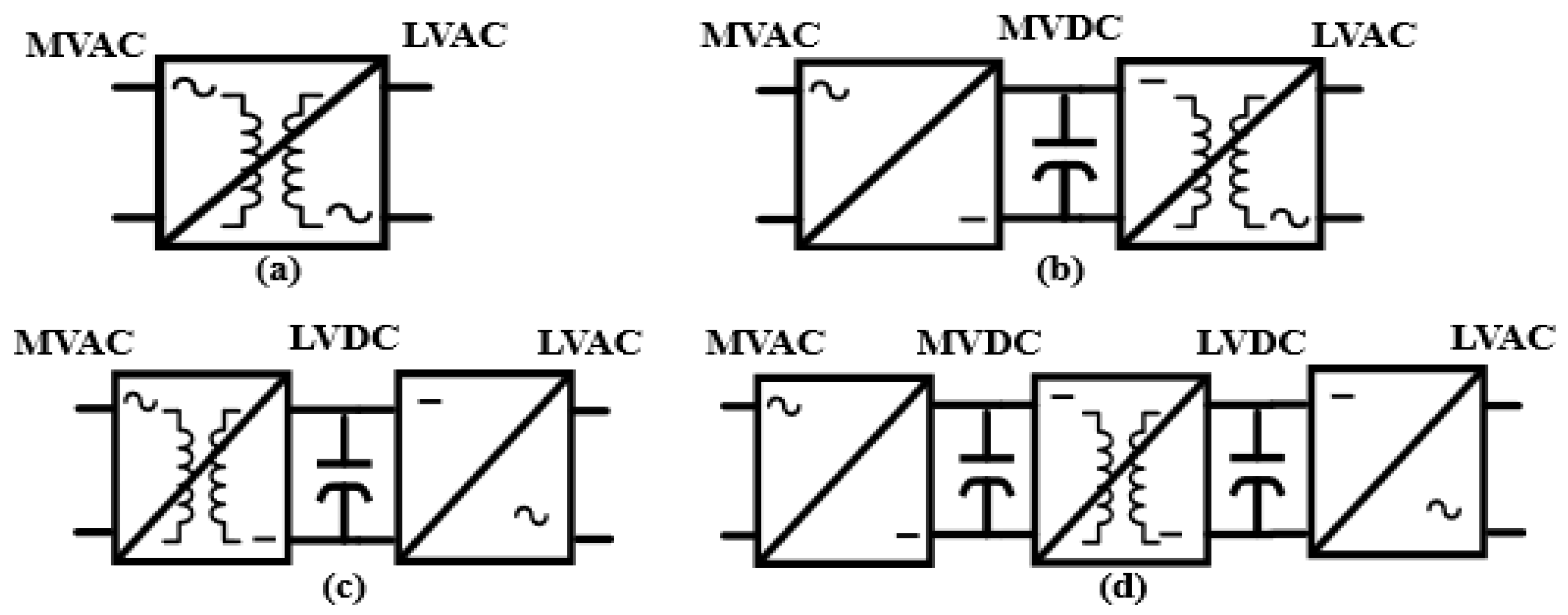
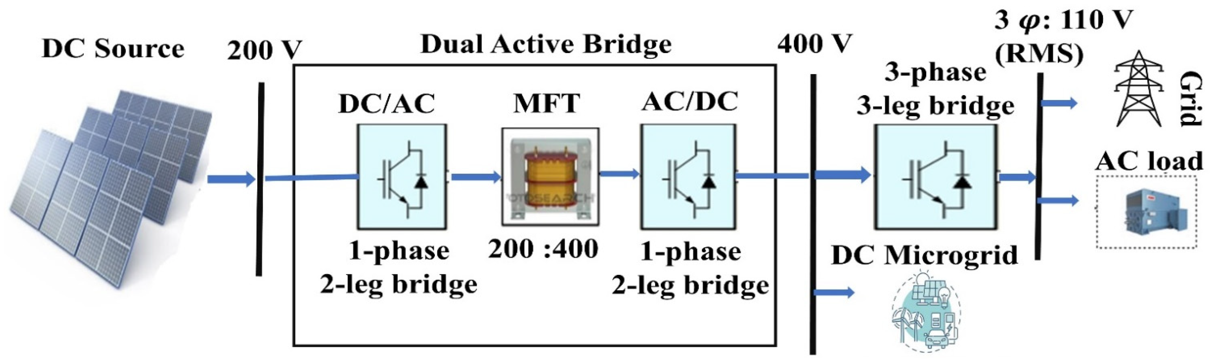
2. Proposed Two-Stage DC-AC SST

The block diagram of the proposed two-stage DC-AC solid-state transformer is illustrated in Figure 2. The designed SST consists of a dual active bridge (DAB) DC-DC converter, followed by a three-phase DC/AC inverter to produce an AC waveform with a desired nominal amplitude and frequency. The specifications of the proposed system are listed in Table 1. The turn ratio of the transformer is chosen to be 1:2 to demonstrate the voltage scaling capability using a DAB. The HV side is chosen to be 400 V to produce a three-phase AC waveform at customer distribution utilization voltages of 120.
Power electronic converters are essential components in the SST. The conventional silicon semiconductor switches consume more power losses compared to the advanced wide bandgap (WBG) semiconductors, i.e., silicon carbide (SiC) and gallium nitrate (GAN) [25]. In this work, the SiC MOSFET is used, as the on/off transition periods are extremely smaller compared to that of silicon-based IGBTs. Therefore, lower switching losses are attained by using SiC MOSFETs [26].

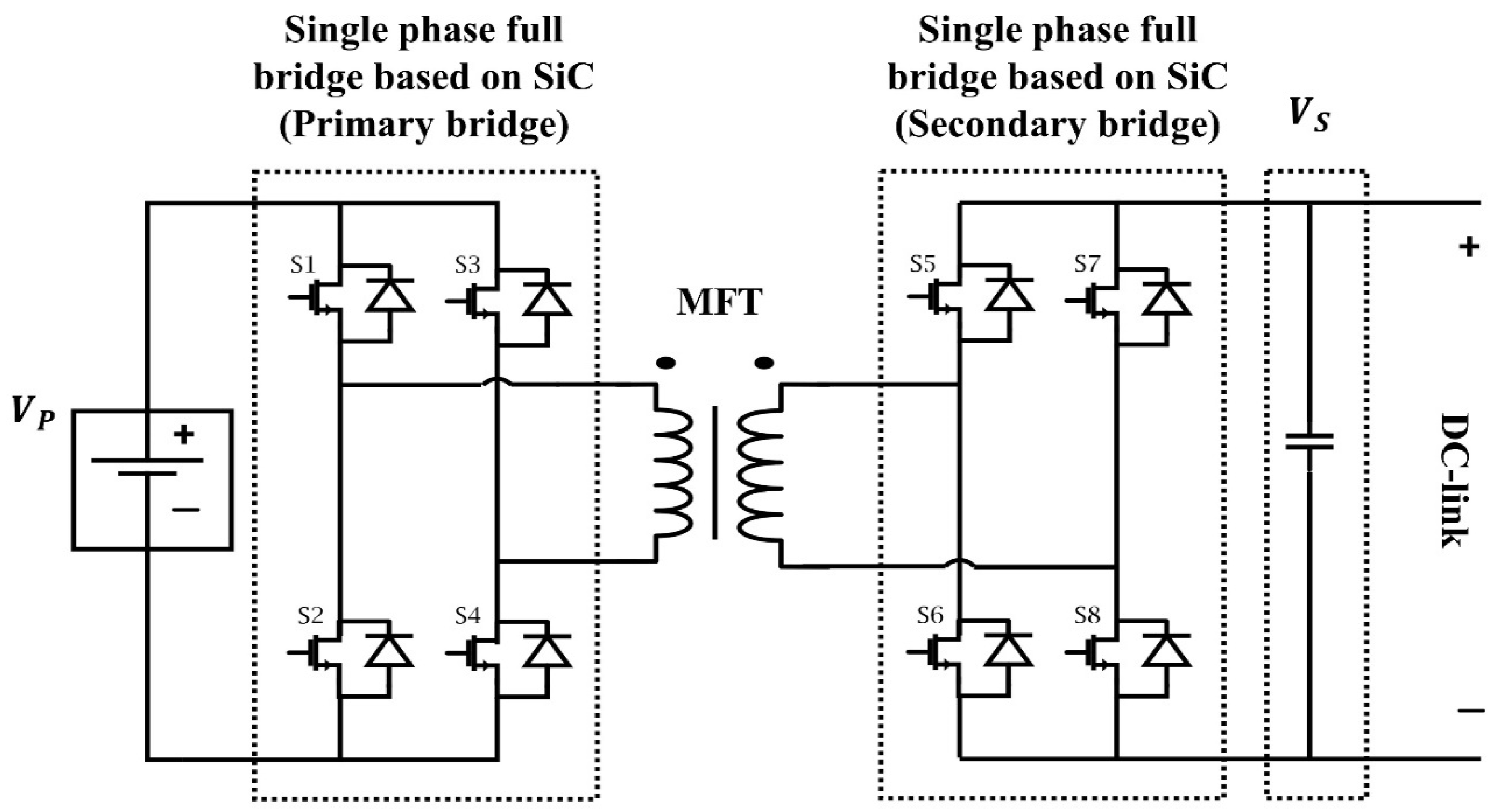
2.1. Dual Active Bridge DC-DC Stage Design

The dual active bridge (DAB) is utilized for the DC-DC stage of the SST in this paper. It consists of a full-bridge converter on the primary and the secondary side with an MF isolation transformer in between, as illustrated in Figure 3.

2.1.1. Operation of DAB

The dual active bridge converter performs three transformations: a DC-AC at the primary input bridge, an AC-AC with the high/medium-frequency transformer in the middle, and an AC-DC at the output bridge. This topology utilizes leakage inductance of the transformer as the main energy transfer element [24]. Several modulation techniques are applied to the DAB, such as single-phase shift modulation, trapezoidal modulation, and triangular modulation [27]. Single-phase shift modulation, also named rectangular modulation, is selected in this paper owing to its low control complexity, lowest RMS current through the transformer, and highest power transfer capability among the prospective contenders [28]. This technique works by commuting the primary and the secondary side switches using square waveforms (duty ratio of 50%) with the diagonal switches in the same bridge turning on/off at the same.
To simplify the steady-state operation analysis, the small series resistances of the equivalent model of the transformer and large magnetizing inductance are neglected. The simplified equivalent circuit of the DAB is shown in Figure 4. The transformer is substituted by the primary-referred equivalent leakage inductance, which is calculated as
  L D A B = L 1 +   L 2 N w 2
where L 1   is the primary inductance of the transformer, L 2   is the secondary inductance of the transformer, N w is the transformer turns ratio, and V S is secondary voltage referred to primary (Figure 4).
The phase shift between the primary and secondary is adjusted to control the power transfer from the leading bridge to lagging bridge. The output average power based on the phase shift can be calculated as [25]
P = V P   · V S   ω   ·   L   ·   N w   · φ   φ 2 π           0 φ   π
This equation expresses the amount of the power delivered from the leading bridge to the lagging bridge as a function of the phase shift, as shown in Figure 5. For a reverse power flow situation, the power transferred is given as [29]
P = V P · V S   ω   ·   L   ·   N w   · φ +   φ 2 π           π φ   0

2.1.2. Transformer Turns Ratio

Assuming that the input voltage of the DAB can vary for a small operating range, the turns ratio is designed based on the nominal input voltage, which is selected in the middle of the input voltage range and the desired output voltage.
N w = V S   V P n o m
One of the main operating parameters is the DC voltage transfer ratio. This ratio defines the mode of operation, and it is calculated as
g = V S N w · V P  
The DAB is operating in buck mode when ( V P > V S )   and in boost mode if ( V P < V S ) . Figure 6 displays the transformer current waveform of the DAP in buck and boost modes.

2.1.3. DC Link Capacitor Design

With the proposed SST rated at 2 kW, the full load output DC current is computed as 5 A. The switching frequency of the DAB is selected to be 20 kHz. The required filter capacitor for the DAB on the HV side can be approximated by (8), assuming that the capacitor voltage ripple and inductor current ripple are 10% and 20%, respectively:
C M V =   Δ I 8 ·   f · Δ V = 380   μ F  
However, its value is chosen 470 μF for the sake of fair comparison with the experimental setup, which consists of full-bridge converters with film capacitors with a 470 μF fixed capacitance, as discussed in Section 4.

2.1.4. Controller Design
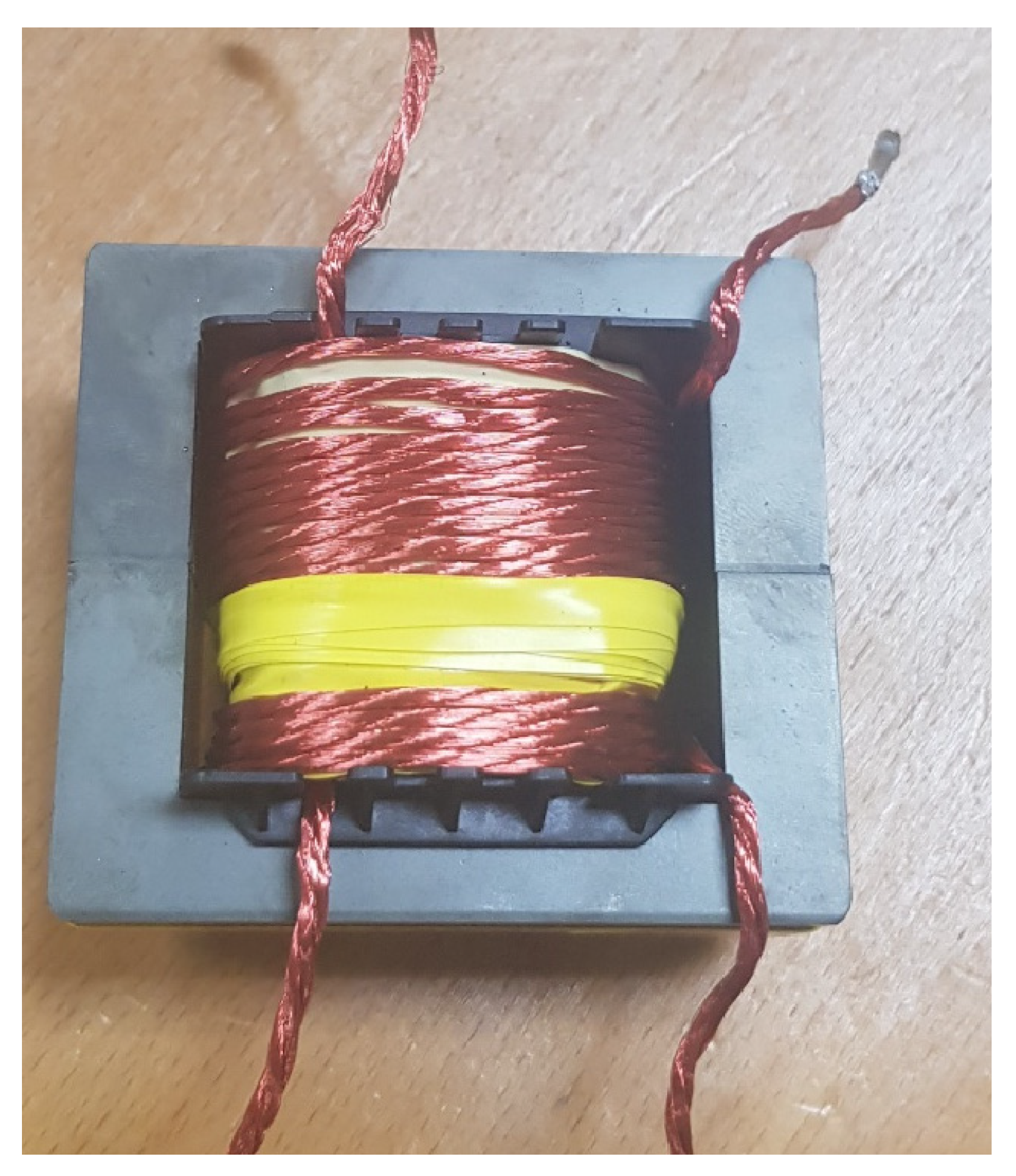
The dual active bridge converter is modeled with closed-loop control based on a simple, independent voltage control loop, as displayed in Figure 7. The control design is based on a full-order continuous time model proposed by [30] using the generalized average modeling technique. MATLAB SISOTOOL was used to tune the controller PI values for better dynamic response. The controller parameters are listed in Table 2.

2.2. MFT Design

The isolation stage contains the HF/MF transformer, which represents the main part of the SST. As mentioned above, each topology in the DC-DC stage of the SST demands a specific leakage inductance for optimal power transfer. Therefore, the desired leakage inductance needs to be integrated in the designed transformer, otherwise an external inductor is required, leading to increased overall volume. For the DAB, the minimum required leakage inductance can be obtained as [27]
L k d =   V P m i n ·   V S   ·   φ m a x   · π φ m a x   2   ·   P m a x   ·   f s ·   π 2 ·   N w
where V P m i n   is the minimum of the primary input voltage range, V S is the desired secondary output voltage, and φ m a x is the maximum operating phase shift.
In general, transformer size, losses, and temperature rise are the main parameters to be optimized in transformer design approaches. However, these characteristics are inter-related, and modifying one can have an impact on the others. Reduced core volume, for example, can reduce core losses while also raising the temperature of the core hot spot. Due to the vast number of design factors, the complexity of the loss model, and the variety of magnetic core shapes, transformer manual design becomes challenging and time-consuming, thus optimization techniques need to be used in the design problem. The MFT optimization aims at maximizing the efficiency, minimizing the total transformer volume, and constructing a transformer with less error between the desired and achieved leakage inductance. Therefore, the optimization problem has three objective functions ( N o b j = 3 ):
f m i n   x = f 1 x   m i n   + f 2 x   m i n   + f 3 x   m i n
where
f 1 x = m a x x   η x = m i n x   P c x + P w x
f 2 x = m i n x   V t x = m i n x   V c x + V w x
f 3 x = m i n x   [   L k d L k c x L k d ]
where η is the efficiency, which is the sum of the core ( P c ) and copper losses ( P w ) .
V t is the total volume, which consists of the core volume ( V c ) and winding volume ( V w ) . The detailed parameters of P c , P w , V c , and V w are given in ref [31,32]. The last objective, as stated above, is that each topology in the DC-DC stage demands a specific leakage inductance for optimal power transfer. Therefore, the desired leakage inductance needs to be integrated in the designed transformer. L k d   and   L k c are the desired and calculated leakage inductance, respectively.
According to the required converter specification of the DC-DC stage in Table 1 and the calculated desired leakage inductance in (6), all specifications needed for an MFT design are presented in Table 3. In this paper, the MFT used with the DAB converter is optimized based on multi-objective transformer design optimization to minimize the volume, maximize the efficiency, and construct a transformer with desired leakage inductance for the operation of the dual active bridge converter (DAB), which are all solved using the nondominated genetic algorithm (NSGA II). Generally, there is no one optimal solution to the multi-objective optimization problem. Instead, a set of optimal solutions (known as Pareto fronts) is generated. Each point of these Pareto fronts represents an optimal medium-frequency transformer design that satisfies all the constraints. One specific solution of these Pareto fronts needs to be chosen for a practical design. Therefore, it is left for the designer to select the best solution that fits their needs based on the targeted application.
For the required maximum power transfer in DAB operation, the leakage inductance is a priority [33]. Therefore, the accurate calculated leakage inductance solution is selected for the design of the transformer. This solution can achieve a leakage inductance of 73.96 μH, substituting the need for an additional inductor for the operation of the proposed dual active bridge. Table 4 presents the main characteristics of the optimized transformer parameters of an accurate leakage inductance solution.
The transformer prototype was built using precast components. These components are an EE core, a former, litz wire, polyester tape, and mounting components. The final constructed transformer prototype is illustrated in Figure 8. The DC resistances and inductances of transformer windings are measured by an LCR meter from PK Precision (Model 889A) and the results are shown in Table 5.

2.3. Three-Phase Inverter DC-AC Stage Design

The DC-AC stage performs the conversion from DC voltage to AC voltage. The function of this stage is the transformation and control of the output to a sinusoidal waveform with a desired amplitude and frequency free from any disturbances. The three-phase full-bridge topology maintains superior performance in the DC-AC stage, and it is mainly selected to interface AC microgrids along with supplying an urban area variable speed electrical drive system. The circuit diagram of the simulated three-phase inverter is shown in Figure 9. The HV side of the DAB (400 V) is the input of the three-phase inverter. Assuming a modulation index ( M a ) of 0.8, the RMS value of the AC output phase voltage is given by
V L N   , r m s = M a · V d c 2 · 2 110   V  
which represents the AC phase waveform at customer distribution utilization voltages. Therefore, the proposed SST can generate a low-frequency (50 Hz) three-phase sinusoidal AC output of 110   V r m s . The switching frequency of the inverter is assumed to be 10 kHz, which is reasonable for the SST applications.

2.3.1. LC Filter Design

With the proposed SST rated at 2 kW, the full load AC output current is calculated as 8.6 A. The LC filter is used to keep the inverter output voltage within a limited range. The filter components are computed with a maximum output current ripple of 20% [34]:
L =   V d c 4 ·   f s w · Δ   I p p , m a x   3   mH    
The cut-off frequency is assumed to be one tenth the switching frequency, thus the required capacitor value is given by
C =   ( 1 2 · π ·   f c ) 2 · 1 L   8.4   μ F
For a fair comparison with the experimental results, the values of the LC filter for the simulation part are chosen to be 2.5   mH ,   8   μ F , based on the components available in the power laboratory. All specifications of the three-phase inverter with LC filters are listed in Table 6.

2.3.2. Controller Design

The three-phase inverter is modeled with a closed-loop control strategy based on the synchronous reference frame (SRF). The capacitor voltage dynamics in the dq frame is given by the following equation [35,36]:
C d V d d t = C ω V q + I d I L d
C d V q d t = C ω V d + I q I L q
These led to the following reference current after replacing the derivative part with the PI controller:
I d r e f = U d C ω V q + I L d
I q r e f = U q + C ω V d + I L q
where U d   and   U q are the output of PI controller.
The inner current dynamics of the three-phase DC-AC converter in the steady state is denoted by the following equations [37,38,39]:
L d i d d t = L ω I q + V T d
L d i q d t = L ω I d + V T q
These led to the following converter voltages after replacing the derivative part with the PI controller:
V T d = U U d L ω I q
V T q = U U q + L ω I d
U U d   and   U U q are the output of PI controller.
Finally, the modulated signals produce the pulse width modulated gate signals after comparing with the triangular carrier signal. The controller block diagram is described in Figure 10, while the controller parameters are summarized in Table 7. The controller parameters were designed based on ref [36,37].

3. Simulation Results

The proposed SST was developed in MATLAB Simulink. The designed controllers of each stage of the SST were tested under three conditions:
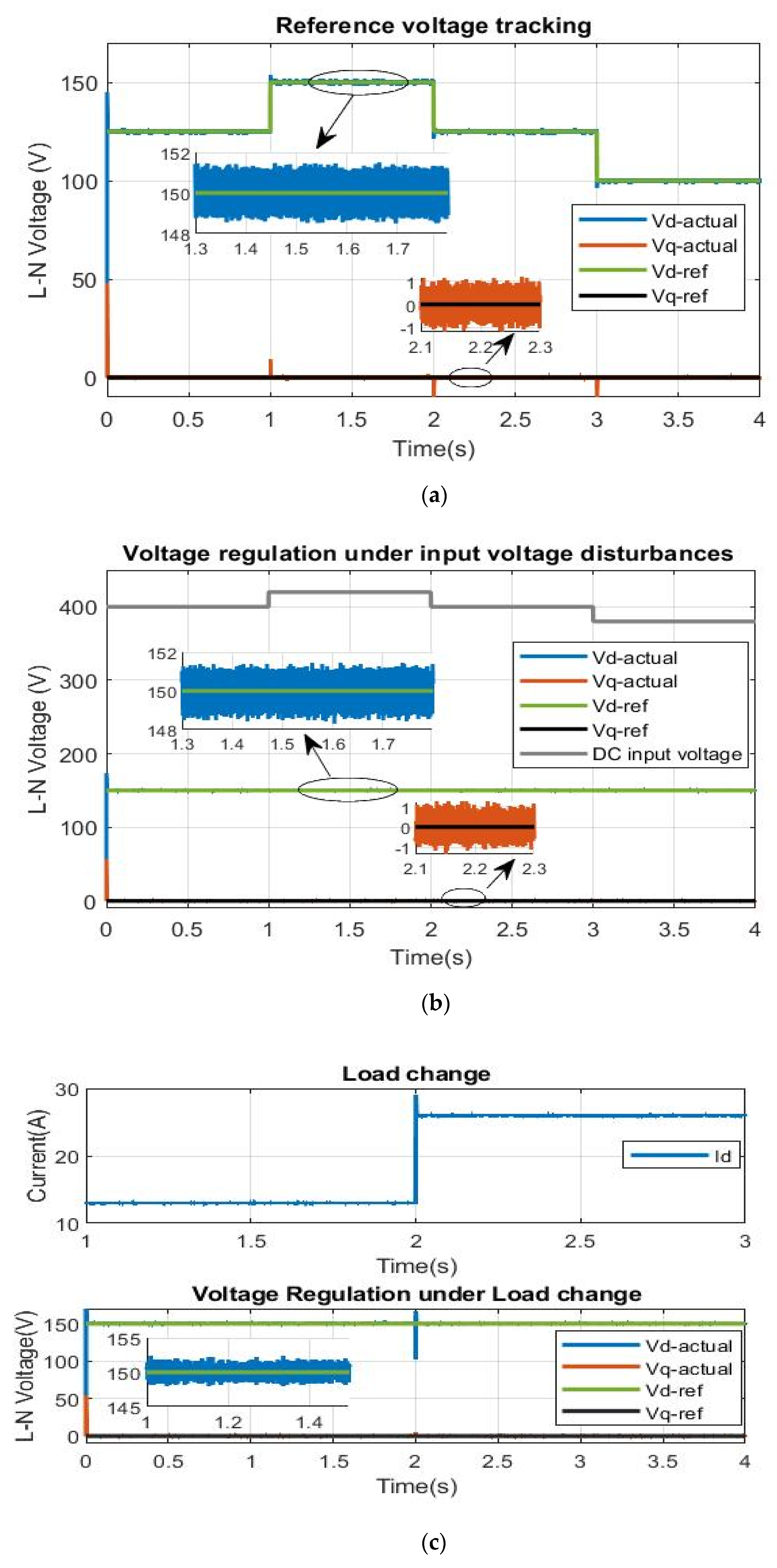
  • Voltage reference tracking.
  • Voltage regulation under input voltage disturbances.
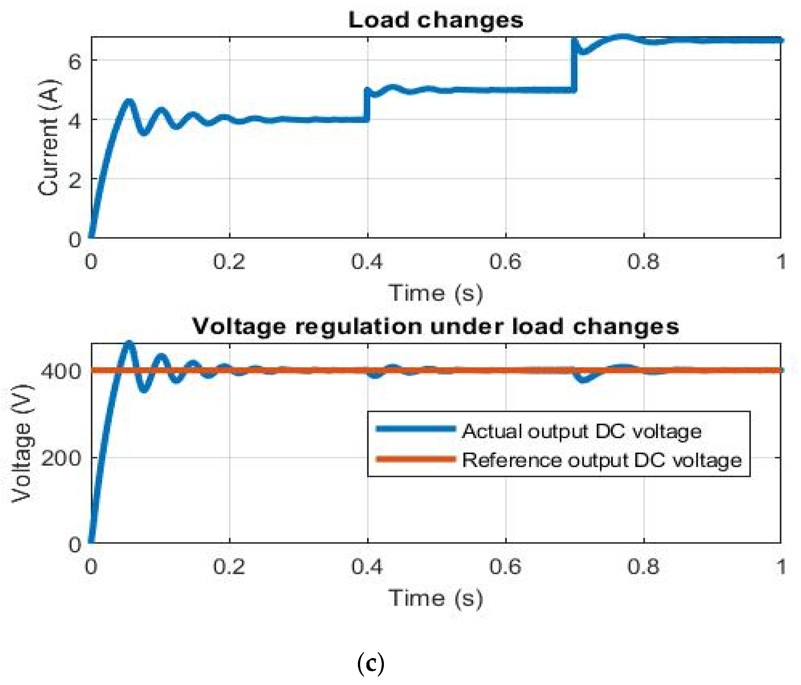
  • Voltage regulation under load changes.

3.1. Dual Active Bridge DC-DC Stage Results

The simulated parameters of the equivalent model of the transformer were set based on the constructed transformer measured by the LCR meter, as inserted in Table 5. The test parameters are tabulated in Table 8 for the three scenarios. The results are displayed in Figure 11. Ultimately, the dual active bridge with its simple PI controller is able to maintain the desired output reference voltage with a stable regulated waveform under the three cases. In addition, the DC outputs have a low ripple voltage, which is in accordance with the design.

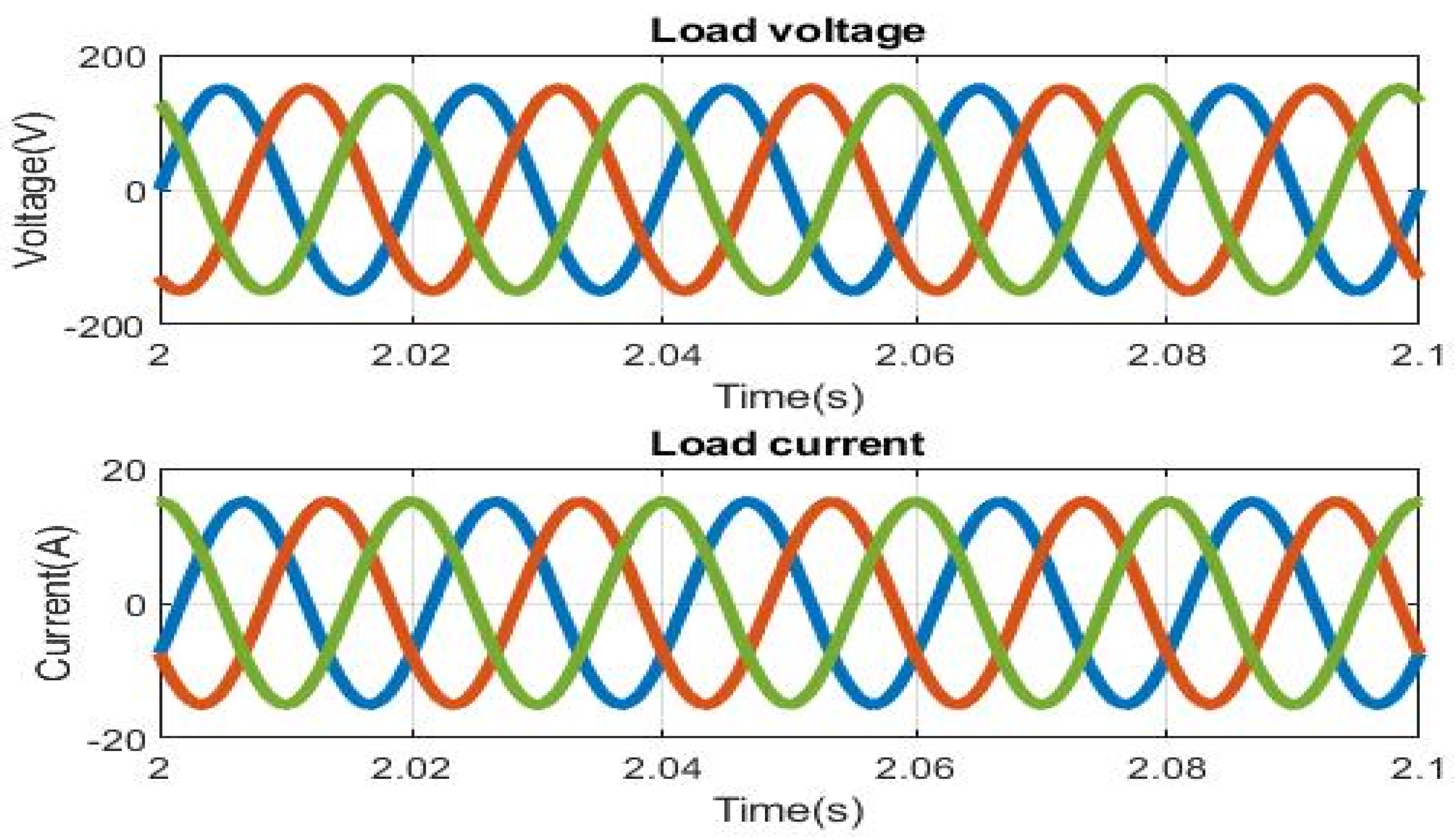
3.2. Three-Phase Inverter DC-AC Stage Results

The results of the simulation model for the three conditions under consideration are displayed in the following figures based on dq components. The test parameters are tabulated in Table 9 for the three scenarios. The results are displayed in Figure 12. The results of the three cases presented above prove that the designed controller exhibits superior performance. In addition, the controllers developed are effective in tracking the desired reference voltage with minimal settling time and rise time. It is clear from Figure 13 that the controller produces a well-regulated, stable sinusoidal waveform. Further, the harmonic spectrum of the output current is analyzed, and the total harmonic distortion (THD) is recorded to be 0.49%.

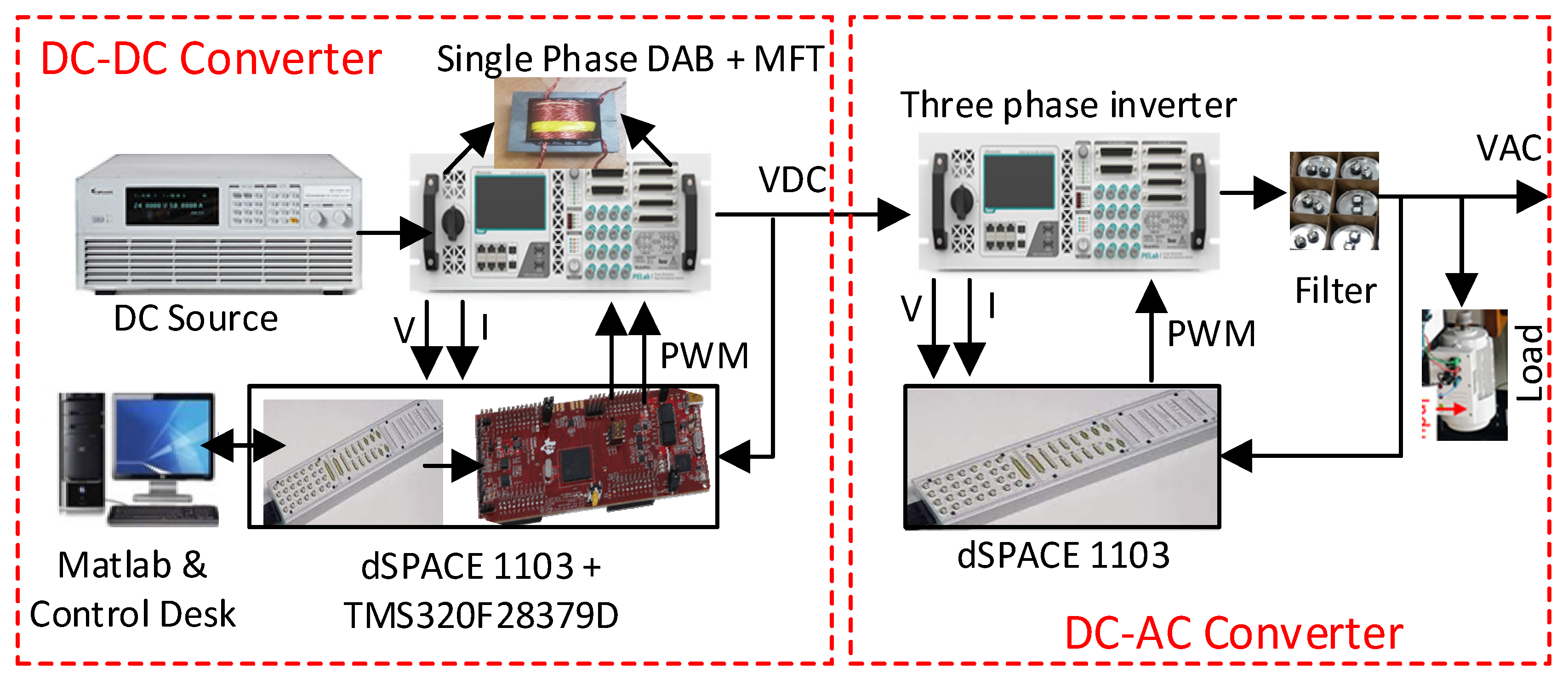
4. Experimental Results

Additionally, in order to validate the designed controllers in the previous section, the same three cases depicted in the simulation study were repeated using the developed experimental setup in real-time implementation. The block diagram of the experimental setup for closed-loop control of the DC link voltage of the DAB and DC-AC voltage regulator are shown in Figure 14.
This section also provides a detailed description of the developed experimental setup. Figure 15 demonstrates the main devices in the physical setup bench.
The dual active bridge topology was modeled by two full-bridge converters based on SiC switches from Taraz technologies (Model # PElab-MMC), whereas the DC-AC stage was constructed by a three-phase inverter (Model Pelab-6PH). The Pelab system is a modular power electronics development. It has a built-in AC inductor, DC capacitors, gate driver circuits, and measurement sensors. The AC inductors were used for LC filters in the DC-AC stage experiment, and the DC capacitors were employed for the DC link in the DAB. The proposed control algorithm requires the measurements of the DC link voltage for the DC-DC dual active bridge, while the DC-AC stage controller is fed by three-phase inductor currents and three-phase output voltage signals. All measurements circuits were designed based on high slew-rate instrumentation amplifiers to attain accurate feedback signals.

4.1. Converters

The control scheme was implemented in real time using the dSPACE 1103 platform. dSPACE is equipped with A/D converters for processing the measured signals and transmitting them to the DSP board where the control algorithm is executed. The digital outputs of dSPACE are connected to drive the converters (0/5 V logic). Similarly, the measured voltage and current are feedbacked to dSPACE for the corresponding control action. The control action (phase shift) of the DAB converter is sent as a 64-bit digital output from dSPACE to the TMS320F28379D controller platform (digital inputs). The task of generating 20 kHz pulses with phase-shifted pulses to drive the DAB is performed by TMS320F28379D, as captured by the Digilent digital discovery kit in Figure 16. The upper four pulses are for the first full-bridge converter, whereas the lower four phase-shifted pulses are for the second full-bridge converter.
The code generation was performed by MATLAB after the control algorithm was designed in MATLAB Simulink. The measured signals were monitored and recorded using the dSPACE Control Desk 6.4 program on the host PC. The simulated control algorithm was configured with same sampling time in a real-time environment.

4.2. Load

Adjustable resistive load was used for the DC-DC stage experiment. On the other side, the three-phase induction motor was connected in parallel with the resistive load when conducting the DC-AC inverter test.

4.3. Dual Active Bridge DC-DC Stage Results

The same control scheme and parameters in the simulation were implemented in real time. The same three tests described in the simulation study were repeated. The results of the experimental model for the three cases are displayed in Figure 17. The test parameters are tabulated in Table 10 for the three scenarios.
As shown in the figures of the three cases, the developed controllers for the dual active bridge topology are autonomous and effective in tracking the desired output reference voltage experimentally. In addition, the test results presented above show that the DC outputs have a low ripple voltage. The AC transformer primary current is measured and plotted in Figure 18, which is consistent with the theoretical waveform of the dual active bridge in Figure 6.

4.4. Three-Phase Inverter DC-AC Stage Results

The results of the experimental test for the three considered transient cases are displayed in Figure 19 based on the same controller designed for the simulation part. The test parameters are tabulated in Table 11 for the three scenarios.
It is clear from the above figures that the three-phase inverter exhibits a better dynamic response with fast tracking capability in all three cases. Therefore, the controller scheme proves its superior performance experimentally and the slower response compared with the simulation is due to the delay, the error introduced by the measurement tools, and how the measured signals were recorded. It can be noted from Figure 20 that the controller produces a well-regulated, stable sinusoidal voltage and current waveforms in a steady-state response. In the experimental part, the three-phase inverter was loaded by a three-phase induction motor, which initiates small harmonics in the load current.

5. Conclusions

The solid-state transformer (SST) is an emerging technology that has the potential to promote advances in a variety of fields, including smart grids, traction systems, and renewable energy systems (RESs). Compared with a low-frequency transformer, an SST has the advantages of volume reduction, portability, controllability, and the synergy of AC and DC systems. First, the converter’s specifications, including an optimized transformer, were selected based on demonstrating the DAB’s capability to scale voltage to deliver a high DC link voltage, which was then converted to distribution-level voltage via a DC-AC converter. The PI and dq controllers were simulated and validated experimentally for the DC-DC and DC-AC conversion. For both stages, lower ripple voltage, less overshoot, and almost zero steady-state error were achieved during the reference voltage tracking. In addition, the AC output voltage from the DC-AC converter was found to be regulated under DC link voltage disturbances and inductive load changes. The two-stage DC-AC converter can be used to integrate solar or battery energy with the grid. It can also operate as a grid-forming converter, which was conducted in this work by controlling voltage. Similarly, the SST based DC-DC converter can be utilized to form a battery-based DC microgrid.

Author Contributions

Conceptualization, A.B. and A.S.; Methodology, A.B. and M.A.A.; Software, A.B., M.I.H. and H.B.; Validation, A.B., M.I.H. and H.B.; Formal analysis, A.B., M.I.H. and M.A.A.; Investigation, A.B., M.I.H. and H.B.; Resources, A.S. and M.A.A.; Writing—original draft, A.B.; Writing—review & editing, M.I.H., H.B., A.S. and M.A.A.; Supervision, M.A.A.; Project administration, M.A.A.; Funding acquisition, M.A.A. All authors have read and agreed to the published version of the manuscript.

Funding

This research received no external funding.

Acknowledgments

The authors acknowledge the research support received from the Interdisciplinary Research Center for Renewable Energy and Power Systems (IRC-REPS), Research Institute, King Fahd University of Petroleum & Minerals (KFUPM), Saudi Arabia through Grant No. INRE2314. Furthermore, the authors acknowledge the support of the K.A. CARE Energy Research & Innovation Center (ERIC) at KFUPM.

Conflicts of Interest

The authors declare no conflict of interest.

Nomenclature

SST based DC-DC converter:
L 1   The primary inductance of the transformer
L 2 The secondary inductance of the transformer
N w The transformer turns ratio
V S Secondary voltage referred to primary
φ Phase shift between the primary and secondary voltage
C M V DC link capacitance
f Switching frequency of DC-DC converter
Δ I Ripple current
Δ V Ripple voltage
V P m i n The minimum of the primary input voltage range
V S The desired secondary output voltage
φ m a x The maximum operating phase shift
P m a x   The maximum transferred power
f s Switching frequency of DC-DC converter
Three-phase DC-AC inverter:
V L N ,   r m s Line to neutral RMS voltage
V d c DC link voltage
M a Modulation index
U U d ,   U U q The output of PI controller of current controller
V T d ,   V T q Converter output voltage in dq frame
R, LArm reactor resistance and inductance
ω Converter angular frequency
V d   &   V q d-q axis voltage
i d   &   i q d-q axis inductor current
I L d ,   I L q d-q axis loads current
CAC side filter capacitance
V d   &   V q d-q axis voltage
U d ,   U q The output of PI controller of voltage controller
  f c Line frequency
  f s w Switching frequency of three-phase inverter
Δ   I p p , m a x Inductor ripple current.

References

  1. Hossain, M.I.; Shafiullah, M.; Abido, M.A. Battery Power Control Strategy for Intermittent Renewable Energy Integrated Modular Multilevel Converter-Based High-Voltage Direct Current Network. Sustainability 2023, 15, 2626. [Google Scholar] [CrossRef]
  2. Liserre, M.; Buticchi, G.; Andresen, M.; De Carne, G.; Costa, L.F.; Zou, Z.X. The Smart Transformer: Impact on the Electric Grid and Technology Challenges. IEEE Ind. Electron. Mag. 2016, 10, 46–58. [Google Scholar] [CrossRef]
  3. Khan, S.; Rahman, K.; Tariq, M.; Hameed, S.; Alamri, B.; Babu, T.S. Solid-State Transformers: Fundamentals, Topologies, Applications, and Future Challenges. Sustainability 2021, 14, 319. [Google Scholar] [CrossRef]
  4. She, X.; Huang, A.Q.; Burgos, R. Review of solid-state transformer technologies and their application in power distribution systems. IEEE J. Emerg. Sel. Top. Power Electron. 2013, 1, 186–198. [Google Scholar] [CrossRef]
  5. Hannan, M.A.; Ker, P.J.; Lipu, M.S.H.; Choi, Z.H.; Rahman, M.S.A.; Muttaqi, K.M.; Blaabjerg, F. State of the art of solid-state transformers: Aadvanced topologies, implementation issues, recent progress and improvements. IEEE Access 2020, 8, 19113–19132. [Google Scholar] [CrossRef]
  6. Shamshuddin, M.A.; Rojas, F.; Cardenas, R.; Pereda, J.; Diaz, M.; Kennel, R. Solid state transformers: Concepts, classification, and control. Energies 2020, 13, 2319. [Google Scholar] [CrossRef]
  7. Adabi, M.E.; de Catalunya, B.U.P.; Martinez-Velasco, J.A. Solid state transformer technologies and applications: A bibliographical survey. AIMS Energy 2018, 6, 291–338. [Google Scholar] [CrossRef]
  8. She, X.; Burgos, R.; Wang, G.; Wang, F.; Huang, A.Q. Review of solid state transformer in the distribution system: From components to field application. In Proceedings of the 2012 IEEE Energy Conversion Congress and Exposition (ECCE), Raleigh, NC, USA, 15–20 September 2012; pp. 4077–4084. [Google Scholar] [CrossRef]
  9. De Silva, H.H.H.; Jayamaha, D.K.J.S.; Lidula, N.W.A. Review on design and control of solid state transformer based microgrids. AIMS Energy 2019, 7, 901–923. [Google Scholar] [CrossRef]
  10. Hossain, I.; Abido, M.A. Active Power Control of PV-Battery Connected MMC-HVDC System for FRT Support. Appl. Sci. 2020, 10, 7186. [Google Scholar] [CrossRef]
  11. Hossain, I.; Abido, M.A. Positive-Negative Sequence Current Controller for LVRT Improvement of Wind Farms Integrated MMC-HVDC Network. IEEE Access 2020, 8, 193314–193339. [Google Scholar] [CrossRef]
  12. Falcones, S.; Mao, X.; Ayyanar, R. Topology comparison for Solid State Transformer implementation. In Proceedings of the IEEE PES General Meeting, Minneapolis, MN, USA, 25–29 July 2010; pp. 1–8. [Google Scholar]
  13. Sabahi, M.; Hosseini, S.H.; Sharifian, M.B.; Goharrizi, A.Y.; Gharehpetian, G.B. Bi-directional power electronic transformer with maximum power-point tracking capability for induction heating applications. IET Power Electron. 2010, 3, 724–731. [Google Scholar] [CrossRef]
  14. Liu, Y.; Liu, Y.; Abu-Rub, H.; Ge, B. Model predictive control of matrix converter based solid state transformer. Proc. IEEE Int. Conf. Ind. Technol. 2016, 2016, 1248–1253. [Google Scholar]
  15. Bhaskar, R.; Agarwal, V. Dual pid loop controller for HF link inverter in two-stage SST. In Proceedings of the 2016 IEEE 7th Power India International Conference (PIICON), Bikaner, India, 25–27 November 2016; pp. 54–57. [Google Scholar]
  16. Besselmann, T.; Mester, A.; Dujic, D. Power Electronic Traction Transformer: Efficiency Improvements Under Light-Load Conditions. IEEE Trans. Power Electron. 2013, 29, 3971–3981. [Google Scholar] [CrossRef]
  17. Lai, J.-S.; Maitra, A.; Goodman, F. Performance of a Distribution Intelligent Universal Transformer under Source and Load Disturbances. In Proceedings of the Conference Record of the 2006 IEEE Industry Applications Conference Forty-First IAS Annual Meeting, Tampa, FL, USA, 8–12 October 2006; pp. 719–725. [Google Scholar]
  18. Ruiz, F.; Perez, M.A.; Espinosa, J.R.; Gajowik, T.; Stynski, S.; Malinowski, M. Surveying solid-state transformer structures and controls: Providing highly efficient and controllable power flow in distribution grids. IEEE Ind. Electron. Mag. 2020, 14, 56–70. [Google Scholar] [CrossRef]
  19. Bifaretti, S.; Zanchetta, P.; Watson, A.; Tarisciotti, L.; Clare, J.C. Advanced Power Electronic Conversion and Control System for Universal and Flexible Power Management. IEEE Trans. Smart Grid 2011, 2, 231–243. [Google Scholar] [CrossRef]
  20. Acikgoz, H.; Kececioglu, O.F.; Karadol, I.; Gani, A.; Sekkeli, M. Adaptive Control of Solid State Transformer Using Type-2 Fuzzy Neural System. Stud. Informatics Control 2017, 26, 171–181. [Google Scholar] [CrossRef]
  21. Acikgoz, H.; Kececioglu, O.F.; Yildiz, C.; Gani, A.; Sekkeli, M. Performance analysis of electronic power transformer based on neuro-fuzzy controller. SpringerPlus 2016, 5, 1350. [Google Scholar] [CrossRef] [PubMed]
  22. Hooshmand, R.A.; Ataei, M.; Rezaei, M.H. Improving the dynamic performance of distribution electronic power transformers using sliding mode control. J. Power Electron. 2012, 12, 145–156. [Google Scholar] [CrossRef]
  23. Sahoo, B.; Routray, S.K.; Rout, P.K. Artificial Neural Network-Based PI-Controlled Reduced Switch Cascaded Multilevel Inverter Operation in Wind Energy Conversion System with Solid-State Transformer. Iran. J. Sci. Technol. Trans. Electr. Eng. 2019, 43, 1053–1073. [Google Scholar] [CrossRef]
  24. Segaran, D.S. Dynamic Modelling and Control of Dual Active Bridge Bi-Directional DC-DC Converters for Smart Grid Applications. Ph.D. Thesis, Monash University, Melbourne, Australia, 2006. [Google Scholar]
  25. Wang, J.; Huang, A.Q.; Sung, W.; Liu, Y.; Baliga, J. Development of 15-kV SiC IGBTs and Their Impact on Utility Applications. IEEE Ind. Mag. 2009, 3, 16–23. [Google Scholar] [CrossRef]
  26. Huber, J.E.; Kolar, J.W. Solid-State Transformers: On the Origins and Evolution of Key Concepts. IEEE Ind. Electron. Mag. 2016, 10, 19–28. [Google Scholar] [CrossRef]
  27. Seyezhai, R. Performance Evaluation of Modulation strategies for Dual Active Bridge Multiport DC-DC Converter. IOSR J. Eng. 2011, 1, 77–83. [Google Scholar] [CrossRef]
  28. Guo, Z. Modulation Scheme of Dual Active Bridge Converter for Seamless Transitions in Multiworking Modes Compromising ZVS and Conduction Loss. IEEE Trans. Ind. Electron. 2020, 67, 7399–7409. [Google Scholar] [CrossRef]
  29. Fan, H.; Li, H. High-Frequency Transformer Isolated Bidirectional DC–DC Converter Modules with High Efficiency Over Wide Load Range for 20 kVA Solid-State Transformer. IEEE Trans. Power Electron. 2011, 26, 3599–3608. [Google Scholar] [CrossRef]
  30. Qin, H.; Kimball, J.W. Closed-loop control of DC-DC dual active bridge converters driving single-phase inverters. In Proceedings of the 2012 IEEE Energy Conversion Congress and Exposition (ECCE), Raleigh, NC, USA, 15–20 September 2012; pp. 173–179. [Google Scholar]
  31. Hurley, W.G.; Wölfle, W.H. Transformers and Inductors for Power Electronics: Theory, Design and Applications; John Wiley & Sons: Hoboken, NJ, USA, 2013. [Google Scholar]
  32. McLyman, C.W.T. Transformer and Inductor Design Handbook, 3rd ed.; CRC Press: Boca Raton, FL, USA, 2004. [Google Scholar] [CrossRef]
  33. Zhao, B.; Song, Q.; Liu, W.; Sun, Y. Overview of Dual-Active-Bridge Isolated Bidirectional DC–DC Converter for High-Frequency-Link Power-Conversion System. IEEE Trans. Power Electron. 2013, 29, 4091–4106. [Google Scholar] [CrossRef]
  34. Shri, A. A Solid-State Transformer for Interconnection between the Medium- and the Low-Voltage Grid Design, Control and Behavior Analysis Challenge the Future. Master’s Thesis, DELFT University, Delft, The Netherlands, 2013. [Google Scholar]
  35. Hossain, M.I.; Abido, M.A.; Pathan, M.I. PMSG Based Wind Energy Integration into MMC Based HVDC Transmission Network in RTDS. In Proceedings of the 2020 IEEE Electric Power and Energy Conference, EPEC, Edmonton, AB, Canada, 9–10 November 2020. [Google Scholar] [CrossRef]
  36. Liu, Z.; Liu, J.; Zhao, Y. A Unified Control Strategy for Three-Phase Inverter in Distributed Generation. IEEE Trans. Power Electron. 2013, 29, 1176–1191. [Google Scholar]
  37. Yazdani, A.; Iravani, R. Voltage-Sourced Converters in Power systems: Modeling, Control, and Applications; IEEE Press: Piscataway, NJ, USA; John Wiley: Hoboken, NJ, USA, 2010. [Google Scholar]
  38. Hossain, I.; Shafiullah; Abido, M. VSC Controllers for Multiterminal HVDC Transmission System: A Comparative Study. Arab. J. Sci. Eng. 2020, 45, 6411–6422. [Google Scholar] [CrossRef]
  39. Hossain, I.; Shafiullah; Al-Sulaiman, F.A.; Abido, M.A. Comprehensive Analysis of PV and Wind Energy Integration into MMC-HVDC Transmission Network. Sustainability 2022, 15, 253. [Google Scholar] [CrossRef]
Figure 1. SST architectures: (a) single-stage SST; (b) two-stage SST with MVDC link; (c) two-stage SST with LVDC link; and (d) three-stage SST.
Sustainability 15 07345 g001
Figure 2. Block diagram of the proposed two-stage DC-AC solid-state transformer.
Sustainability 15 07345 g002
Figure 3. Dual active bridge DC-DC converter.
Sustainability 15 07345 g003
Figure 4. An equivalent approximated model of the DAB referred to primary side.
Sustainability 15 07345 g004
Figure 5. Dual active bridge power transfer characteristic.
Sustainability 15 07345 g005
Figure 6. Voltage and flux density operating waveforms of DAB in buck and boost modes.
Sustainability 15 07345 g006
Figure 7. Controller block diagram for dual active bridge converter.
Sustainability 15 07345 g007
Figure 8. Final constructed MFT 2 kW prototype.
Sustainability 15 07345 g008
Figure 9. Three-phase full-bridge inverter.
Sustainability 15 07345 g009
Figure 10. Controller block diagram for three-phase inverter.
Sustainability 15 07345 g010
Figure 11. Simulation results of dual active bridge DC-DC stage for the three cases: (a) voltage reference tracking; (b) voltage regulation under input voltage disturbances; (c) voltage regulation under load changes.
Sustainability 15 07345 g011aSustainability 15 07345 g011b
Figure 12. Simulation results of DC-AC stage control for the three cases: (a) voltage reference tracking; (b) voltage regulation under input voltage disturbances; (c) voltage regulation under load changes.
Sustainability 15 07345 g012
Figure 13. Voltage and current waveforms of load for the simulation DC-AC stage control.
Sustainability 15 07345 g013
Figure 14. Experimental setup for closed-loop control of DC link voltage of DAB and AC voltage regulator.
Sustainability 15 07345 g014
Figure 15. Main devices in the experimental setup.
Sustainability 15 07345 g015
Figure 16. Generating 20 kHz pulses through TMS320F28379D.
Sustainability 15 07345 g016
Figure 17. Experimental results of DC-DC stage control for the three cases: (a) voltage reference tracking; (b) voltage regulation under input voltage disturbances; (c) voltage regulation under load changes.
Sustainability 15 07345 g017
Figure 18. Transformer primary AC waveform current (experimental).
Sustainability 15 07345 g018
Figure 19. Experimental results of DC-AC stage control for the three cases: (a) voltage reference tracking; (b) voltage regulation under input voltage disturbances; (c) voltage regulation under load changes.
Sustainability 15 07345 g019aSustainability 15 07345 g019b
Figure 20. Voltage and current waveforms of load for the experimental DC-AC stage control: (a) voltage waveform; (b) current waveform.
Sustainability 15 07345 g020
Table 1. Specifications of the proposed two-stage DC-AC SST.
ParameterSymbolValue
Power rating P o 2 kW
DC-DC stage (using dual active bridge topology)
Input voltage (primary input side) V P d a b 200 V
Output voltage (secondary output side) V S d a b 400 V
DC-AC stage (using 3-leg converter topology)
Input voltage V i n i n v 400 V
Output line voltage V o i n v 110 V RMS
Table 2. Dual active bridge controller parameters.
ParameterSymbolValue
Sampling time T s 1 μ sec
Proportional gain k p 0.306
Integral gain k i 90
Maximum phase shift φ m a x 72 o
Table 3. Typical specifications of DAB converter.
ParameterSymbolValue
Switching frequency f s d a b 20 kHz
Apparent power S n d a b 2585 VA
Output power P o d a b 2 kW
Primary DC link voltage V L V d a b 175–200 V
Secondary DC link voltage V H V d a b 400 V
Transformer primary RMS rated current I r 1 13.9 A
Transformer secondary RMS rated current I r 2 5.64 A
Desired leakage inductance L k d 78.8 μH
Table 4. The main characteristics and parameters for the prototype transformer.
ParameterChoice
Core materialFerrite
Material seriesN87
Core structureShell-type
Core dataEE 70/33/32
Core cross sectional area ( A c )6.83 cm2
Window area ( A w ) 5.69 cm2
Core mean length ( l c ) 149 mm
Wire typeRound litz wire
Wire designation3/54/38
Winding dataSplit geometry
Table 5. Transformer equivalent model paraments.
ParameterSymbolValue
Primary wire resistance R 1 0.023 Ω
Secondary wire resistance R 2 0.023 Ω
Leakage inductance referred to primary L k 75.16 μH
Magnetizing inductance referred to primary L m 113.3 μH
Table 6. Three-phase inverter specifications.
ParameterSymbolValue
Switching frequency f s i n v 10 kHz
Maximum output power P o i n v 2 kW
Input voltage V i n i n v 400 V
Output filter inductor L 2.5 mH
Output filter capacitor C 8 μF
Output line voltage V L L 190 V RMS
Table 7. Three-phase inverter controller parameters.
ParameterSymbolValue
Sampling time T s 20 μ sec
Voltage control loop, PI1
Proportional gain k p 0.1
Integral gain k i 100
Current control loop, PI2
Proportional gain k p 30
Integral gain k i 200
Table 8. Test parameters for the simulation of dual active bridge DC-DC stage.
Case StudiesTest Parameters
Input VoltageLoad ResistanceOutput Reference Voltage
Case 1: Voltage
reference tracking
200 V80 Ω350 V, 370 V,
380 V, and 400 V
Case 2: Voltage
regulation under
input voltage
disturbances
150 V, 170 V,
180 V, and 200 V
80 Ω400 V
Case 3: Voltage
regulation under load changes
200 V100 Ω, 80 Ω, and
60 Ω
400 V
Table 9. Test parameters for the simulation of three-phase inverter DC-AC stage.
Case StudiesTest Parameters
Input VoltageLoad ResistanceOutput Reference Phase Voltage
Case 1: Voltage
reference tracking
400 V15 Ω125 V, 150 V,
125 V, and 100 V
Case 2: Voltage
regulation under
input voltage
disturbances
375 V, 400 V, and
425 V
15 Ω150 V
Case 3: Voltage
regulation under load changes
400 V10 Ω, 5 Ω,150 V
Table 10. Test parameters for the experiment of dual active bridge DC-DC stage.
Case StudiesTest Parameters
Input VoltageLoad ResistanceOutput Reference Voltage
Case 1: Voltage
reference tracking
120 V200 Ω250 V, 260 V, 270 V,
280 V, 290 V, and 300V
Case 2: Voltage
regulation under
input voltage
disturbances
85–125 V200 Ω300 V
Case 3: Voltage
regulation under load changes
120 VGradually decrease 3000–300 Ω300 V
Table 11. Test parameters for the experimental of three-phase inverter DC-AC stage.
Case StudiesTest Parameters
Input VoltageLoadingOutput Reference Phase Voltage
Case 1: Voltage
reference tracking
400 V50 Ω125 V, 150 V,
125 V, and 100 V
Case 2: Voltage
regulation under
input voltage
disturbances
375 V, 400 V, and
420 V
50 Ω150 V
Case 3: Voltage
regulation under load changes
400 V0.75 kW, 220 V, and 60 Hz
Induction
motor
150 V
Disclaimer/Publisher’s Note: The statements, opinions and data contained in all publications are solely those of the individual author(s) and contributor(s) and not of MDPI and/or the editor(s). MDPI and/or the editor(s) disclaim responsibility for any injury to people or property resulting from any ideas, methods, instructions or products referred to in the content.

