Abstract
The semiconductor industry is essential to information technology and the ongoing artificial intelligence transformation but also poses significant environmental challenges, including greenhouse gas emissions, air pollution, solid waste, and high water and energy consumption. This review identifies key emission sources in semiconductor manufacturing, focusing on the release of fluorinated gases from chemical-intensive processes and the sector’s substantial energy demands. We evaluate the effectiveness and limitations of current mitigation strategies, such as process optimization, clean energy adoption, and material substitution. We also examine supply chain interventions, including green procurement, logistics optimization, and intelligent management systems. While technological innovation is crucial for the sustainable transition of the global semiconductor industry, the high cost of upgrading to greener production processes remains a major obstacle. Despite progress in clean energy integration and material alternatives, significant challenges persist in reducing emissions across the entire value chain. This review underscores an urgent need for collaborative, integrated approaches to drive the sustainable transition of the semiconductor sector and its upstream supply chain.
1. Introduction
The semiconductor industry is fundamental to contemporary technological advancement, powering everything from mobile phones and computers to electric vehicles and artificial intelligence applications. Driven by surging global demand, the semiconductor market has nearly doubled over the past decade, reaching USD 573 billion in 2022 [1]. Major production hubs include China, the United States, Japan, South Korea, and Europe, each contributing distinct strengths in manufacturing and innovation [2]. Despite rapid growth, this industry faces significant sustainability challenges, particularly due to its substantial environmental impact.
Semiconductor manufacturing is resource-intensive, involving high energy consumption, extensive chemical use, and significant emissions of greenhouse gases, notably fluorinated gases, which possess a high global warming potential. The sector emitted approximately 64.24 million tons of CO2-equivalent gases in 2020 alone [3], accounting for a significant portion of emissions from the broader ICT industry [4]. Emissions in the semiconductor sector are typically classified into three categories: direct emissions from manufacturing processes (Scope 1), indirect emissions from electricity and steam use (Scope 2), and upstream emissions from the supply chain (Scope 3), with a recent study revealing that just 15 major global semiconductor market entities are responsible for 39,763.4 kt of CO2e from Scope 1 and Scope 2 emissions (Figure 1) [2]. Addressing these emissions, particularly the often-overlooked Scope 3 emissions from the supply chain, is crucial for the industry’s sustainable transition.
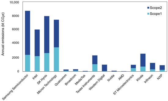
Figure 1.
Scope 1 and Scope 2 emissions of the 15 main semiconductor market entities in 2021.
With growing attention on climate change, industries worldwide are exploring ways to reduce their carbon footprint to address escalating environmental challenges. Indeed, various greenhouse gas (GHG) emissions are present in fuels, feedstocks, heat, and throughout semiconductor production processes, with the most critical emissions arising from process gases such as perfluorocarbons (PFCs), hydrofluorocarbons (HFCs), nitrogen trifluoride (NF3), and sulfur hexafluoride (SF6), all of which possess high global warming potentials. Moreover, certain semiconductor chemicals can contribute to ozone depletion, exhibit exceptionally long atmospheric lifetimes, and pose potential health risks under high-concentration exposures, further exacerbating their overall environmental and human health impacts [5]. Nevertheless, global semiconductor demand is expected to keep growing in the coming decades, driven by the rapid expansion of technologies such as artificial intelligence, electric vehicles, 5G, and the IoT. In light of this, the semiconductor industry faces a significant challenge: how to meet the rising demand for semiconductor products while reducing its environmental impact and addressing the industry’s high energy consumption and GHG emissions.
Despite some studies having significantly advanced our understanding of GHG emissions in the semiconductor industry, a comprehensive global decarbonization framework for semiconductor production has yet to be established. Moreover, while most studies focus narrowly on specific technologies or regional case studies, they often lack an integrated, multi-scale perspective that links process-level innovations with supply chain-wide mitigation and policy-level coordination. Critical dimensions such as Scope 3 emissions, trade-offs between air pollutant abatement and carbon reduction, and the cross-regional scalability of solutions remain underexplored. In addition, the local environmental and health impacts of semiconductor production—particularly air and water pollution and soil contamination—are often overlooked in current decarbonization discussions. In addition, semiconductors are produced and traded globally and exhibit significant regional disparities. These variations require careful consideration of broader implications for national strategies, cost competitiveness, and geopolitical factors in decarbonization efforts. Moreover, some strategies, such as biogas technologies for waste-to-energy conversion and chemical waste stream separation and repurification, remain underexplored and may be incompatible across regions, facilities, and types of environmental impacts. These gaps highlight the urgent need for a systematic and up-to-date review of decarbonization strategies tailored to the unique complexities of the semiconductor industry.
This review aims to systematically examine the environmental impacts of semiconductor manufacturing, including greenhouse gas emissions, air and water pollution, waste generation, and health consequences. It evaluates existing and emerging technologies for emission mitigation, covering chemical processes, production methods, and plant operations. Furthermore, this review explores broader systemic strategies such as circular economy practices, sustainable trade policies, and international cooperation, presenting a comprehensive roadmap to facilitate the sustainable transformation of the global semiconductor industry.
2. Environmental Impacts of Semiconductor Production
Semiconductor production involves substantial resource and energy consumption, leading to significant environmental and human health impacts. First, semiconductor manufacturing generally relies on electricity generated from fossil fuels, resulting in considerable GHG emissions. Additionally, the process involves the use of perfluorocarbons, which have long atmospheric lifetimes and high global warming potentials (GWPs), further exacerbating climate change risks. In addition, semiconductor manufacturing demands large quantities of ultrapure water, placing significant pressure on water resources, especially in water-scarce areas. Meanwhile, untreated wastewater can release toxic chemicals such as heavy metals and volatile organic compounds into local ecosystems, causing water and soil contamination. Moreover, the manufacturing process emits various air pollutants such as VOCs, NOx, SOx, and PM, which negatively impact local air quality and human health.
2.1. Carbon Emissions and Their Sources
To understand the environmental footprint of the semiconductor industry, it is essential to identify the main sources of GHG emissions. Semiconductor production, fundamental to sectors such as electronics, transportation, and communication, involves complex, energy-intensive processes that contribute significantly to carbon emissions (Figure 2a) [6]. Semiconductor manufacturing is generally divided into two stages: the front end of the line, where transistors are created, and the back end of the line, where interconnections are established [7]. The front-end processes, especially wafer fabrication activities such as photolithography, etching, and chemical vapor deposition, are the primary sources of emissions [8]. These processes heavily utilize fluorinated gases such as SF6, NF3, and PFCs, all of which have long atmospheric lifetimes and high global warming potentials. For instance, fluorinated gases account for over 19% of the total semiconductor industry emissions in Taiwan, China (hereafter Taiwan for short) [9,10,11,12].
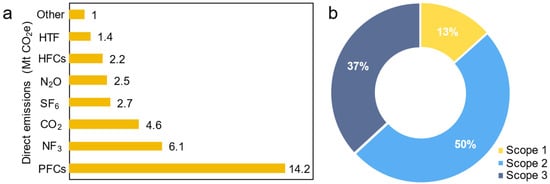
Figure 2.
(a) Different pollutants from the direct emissions of semiconductor manufacturing in 2021; (b) the proportion of Scope 1, Scope 2, and Scope 3 GHG emissions from semiconductor manufacturing companies in Taiwan in 2020.
Indirect emissions from electricity consumption (Scope 2 emissions) also significantly contribute to the industry’s carbon footprint. Wafer fabrication equipment operates under continuous high loads, requiring controlled cleanroom environments and energy-intensive processes such as maintaining high temperatures and pressures, as well as high-volume air conditioning. These processes are typically powered by fossil fuel-generated electricity, substantially adding to the industry’s overall emissions. In Taiwan, Scope 2 emissions alone constitute approximately half of the annual greenhouse gas emissions attributed to semiconductor manufacturing (Figure 2b) [11].
In addition to direct and indirect emissions, emissions from the semiconductor industry’s supply chain (Scope 3 emissions) are significant yet challenging to manage due to their complexity. Scope 3 emissions originate from upstream activities such as manufacturing high-purity chemicals, producing specialized semiconductor equipment, and extracting raw materials such as silicon and rare metals. Each step of the supply chain involves energy-intensive operations, leading to considerable carbon emissions. In Taiwan, for example, upstream supply chain activities contribute about 37% of the industry’s total emissions [12]. Effectively mitigating these emissions requires collaboration among suppliers, enhanced energy efficiency, and the adoption of sustainable, low-carbon materials and processes.
Technological advancements in semiconductor manufacturing also influence emission levels. Research indicates that as semiconductor production technology advances towards smaller, nanometer-scale chips, emissions and resource use per chip can decrease. For example, manufacturing processes for smaller chip sizes (20 nm) typically result in lower greenhouse gas emissions and reduced water use compared to older technologies (30 nm and 40 nm) [13]. As demand continues to grow for enhanced chip performance, lower power consumption, smaller sizes, and faster signal transmission, smaller-node technologies are being further designed and developed, offering additional potential for mitigating the environmental impact of chip production [14,15]. Furthermore, Liu et al. assessed the environmental impacts of various production stages in the DRAM process using the Eco-indicator 95 and IMPACT 2002+ methods. They found that the primary contributor was the diffusion process (19.31–26.52%), followed by photolithography (12.37–25.30%), thin film (23.43–36.54%), etching (20.01–26.48%), and CMP (4.74–5.31%) processes [16]. In addition, the semiconductor packaging process also generates a modest amount of greenhouse gas emissions, in which extensive energy use is the primary source, as operating factories and equipment consumes a large amount of electricity, leading to hundreds of thousands to over a million tons of CO2 emissions per year [8]. Auxiliary materials such as lead frames, substrates, and bonding wires also drive emissions—notably, gold wire bonding has a high carbon cost, so the industry’s shift to copper wires has lowered packaging GHG footprints [17,18].
Overall, addressing semiconductor industry emissions requires a comprehensive approach spanning manufacturing stages, supply chain activities, and technological improvements, highlighting the importance of coordinated strategies for sustainable industry practices (Figure 3).

Figure 3.
The lifecycle of semiconductors.
2.2. Air Pollution and Health Impacts
Semiconductor manufacturing generates a variety of air pollutants beyond greenhouse gases, notably VOCs, acidic gases, and particulate matter (primarily PM10 and smaller), each posing distinct environmental and health risks. Due to the diverse manufacturing processes and production technologies used in the semiconductor industry, the source profiles of different pollutants differ significantly. VOC emissions, for instance, primarily include acetone and isopropanol, which are widely used as cleaning agents, along with smaller amounts of benzene, ethyl acetate, and styrene. These compounds contribute to the formation of photochemical smog and can react with NOx to produce secondary organic aerosols and ozone. Exposure to VOCs can lead to inflammation, respiratory problems, nausea, and damage to the central nervous system and other organs, with potential carcinogenic risks [19]. As a result, reducing VOCs has become a key focus of environmental initiatives in the semiconductor industry [20,21].
Acidic gases primarily originate from etching and cleaning processes, during which chemical reactions release sulfur- and fluorine-based compounds (e.g., H2SO4, HF, HCl, and HNO3). Before being released into the atmosphere, these gases must be treated using scrubbers to mitigate their impact [19]. Acidic gases are highly corrosive and toxic, posing serious health risks such as respiratory and digestive disorders. Environmentally, they contribute to acid rain and soil and water acidification, causing long-lasting ecological harm and altering atmospheric chemical conditions, which may further intensify climate change [19,22,23].
Particulate matter emissions from semiconductor manufacturing typically originate from etching and deposition processes at high temperatures. These operations generate small airborne particles, including metal oxides and other residues, that can linger in the air, increasing risks for workers and nearby communities. Inhalation of PM, especially fine particles with aerodynamic diameters of 2.5 microns or less (PM2.5), has been linked to respiratory and cardiovascular diseases, as well as potential carcinogenic effects depending on particle composition [24]. Additionally, these fine particles can act as carriers for toxic substances such as heavy metals, further exacerbating their health impacts [25,26].
The wafer fabrication stage is particularly intensive in terms of resource use and is the main source of air pollution within semiconductor manufacturing [13]. Etching and deposition processes emit persistent, highly toxic fluorinated gases, while chemical vapor deposition and plasma etching release particulate matter and other hazardous byproducts [27]. In comparison, back-end processes such as chip packaging and testing contribute comparatively lower emissions but still release significant quantities of VOCs and heat-related pollutants [28,29]. This diversity of pollutants across different manufacturing stages underscores the importance of implementing targeted mitigation strategies tailored to each step.
Recent data illustrate trends in emissions from major semiconductor producers, such as the Taiwan Semiconductor Manufacturing Company (TSMC, Hsinchu, Taiwan, China). In 2023, the TSMC reported significant emissions of VOCs, SOx, and NOx, totaling 94.4 metric tons, 40.7 metric tons, and 185.42 metric tons, respectively (Figure 4) [30]. These reports also highlight the historical trends in emissions: VOC emissions remained relatively steady in the mid-2010s, then experienced a sharp drop in 2019 and stabilized at a lower level thereafter. In contrast, NOx emissions increased gradually in the early years and surged substantially between 2019 and 2022, before showing signs of stabilization in 2023. Meanwhile, SOx emissions stayed low throughout this period, with only minor fluctuations. This significant decrease in VOC emissions around 2019 reflects the deployment of more effective VOC abatement measures and the substitution of high-VOC process chemicals at that time, possibly in response to stricter environmental regulations and technology upgrades. For instance, the TSMC implemented advanced emission control technologies (e.g., zeolite rotor concentrators combined with thermal oxidizers) that greatly improved VOC capture efficiency [31]. However, the increased use of high-temperature combustion to destroy VOCs had the side effect of forming more NOx pollutants, as the nitrogen in the air is oxidized at burner temperatures [32]. Additionally, rapid production expansion and greater on-site energy use contributed to the rise in NOx after 2019. By 2023, mitigation steps such as low-NOx burners and optimized scrubbers were introduced to address the elevated NOx [32], highlighting how continuous process improvements are needed to balance multi-pollutant emissions in semiconductor manufacturing.
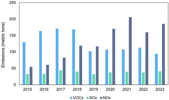
Figure 4.
The changes in VOC, SOx, and NOx emissions from the TSMC in 2015–2023.
2.3. Water Use and Solid Waste Impact
Semiconductor manufacturing is both water-intensive and a major generator of solid waste, emphasizing the need for effective resource management and recycling strategies. The semiconductor production process is highly water-intensive, with manufacturing being the largest consumer of water in the semiconductor lifecycle. Key drivers include cooling systems, the production of ultrapure water (UPW) for wafer rinsing, and HVAC systems in cleanrooms [33,34]. Globally, the industry consumes approximately 210 trillion liters of water annually, with nearly half of this usage occurring in regions already experiencing above-average water scarcity [35].
Between 2017 and 2021, total water consumption across 27 major semiconductor companies increased by over 50%, driven by expanded production capacity and more advanced manufacturing processes [36]. Ultrapure water alone accounts for 87% of total water use in the industry, reaching 551 million cubic meters in 2022 [36]. To optimize water recovery and reuse, it is critical to classify wastewater and apply appropriate water treatment technologies. Numerous advanced technologies have been developed to recycle and reuse wastewater in semiconductor manufacturing, including chemical precipitation for the removal of metals and fluoride, membrane separation and reverse osmosis for fine purification, and evaporation processes for brine concentration. However, the large-scale implementation of these measures remains challenging. The complex composition of wastewater often requires multiple sequential treatments and stringent quality control, while the high energy and cost demands present significant operational barriers. Some leading semiconductor manufacturers have made notable efforts in wastewater recovery. For example, the TSMC has set a target of 90% for water recycling, as well as near-zero liquid discharge systems; Intel has partnered with municipal authorities to build on-site water reclamation facilities; and Samsung is converting municipal wastewater into ultrapure water for chip production [37,38,39]. These initiatives have substantially reduced water waste, mitigated chemical pollution, and lowered the carbon footprint associated with water supply and treatment.
In addition to water use, semiconductor production generates large volumes of solid waste, including hazardous materials. Core materials such as silicon (Si), gallium arsenide (GaAs), cadmium telluride (CdTe), and gallium nitride (GaN) are essential to modern electronics but create byproducts in various forms—solid, liquid, semi-solid, and gaseous [40]. A notable example is an Intel facility in Arizona, which produced about 15,000 tons of waste in just three months, with hazardous materials comprising 60% of the total [41]. These include per- and polyfluoroalkyl substances (PFAS) and slurry from chemical mechanical polishing, which pose serious environmental and health risks if not properly handled [42]. Electronic waste (e-waste) is a growing concern, with 53 million metric tons generated globally in 2019 and only 17% being recycled [43]. This highlights the untapped potential for recovering valuable materials from discarded semiconductors. Increasingly, manufacturers are treating waste as a resource. For instance, the TSMC recovered 10,000 metric tons of copper sulfate waste by reusing semiconductor-grade copper to produce copper tubes, generating both environmental and financial benefits [42]. These practices demonstrate the importance of shifting from a disposal mindset to one focused on resource recovery and circular economy principles, which can support both sustainability and long-term industry viability. The next section will explore technologies enabling semiconductor material recycling in greater detail.
3. Mitigation Technologies and Strategies
GHG emissions in semiconductor manufacturing are mainly categorized into three scopes: Scope 1 (direct emissions), Scope 2 (electricity-related emissions), and Scope 3 (upstream supply chain emissions). Scope 1 emissions mostly consist of process gases, and the primary strategies for mitigating these emissions involve process improvements, material substitution, and gas control systems. Scope 2 emissions mainly result from electricity use, with key mitigation strategies focusing on switching to renewable energy and improving energy efficiency. Scope 3 emissions from the upstream supply chain are challenging to directly mitigate due to the complexity of the supply chain, as even first-tier suppliers may involve hundreds of suppliers, each of which has dozens or even hundreds of second-tier suppliers. Moreover, semiconductor companies often face difficulties in directly requiring or supervising their suppliers’ GHG mitigation efforts. As a result, emissions mitigation strategies specific to each supplier’s industry or government-mandated mitigation requirements are necessary. Many semiconductor manufacturers are exploring ways to mitigate emissions across their supply chains. One notable example is Apple Inc., which has committed to sourcing from over 300 upstream manufacturers that plan to use 100% clean energy by 2030 [44]. These efforts underscore the growing emphasis on renewable energy adoption throughout the supply chain. Furthermore, chemicals—particularly the production of original ultrapure chemicals and materials, which represent a significant component of Scope 3 emissions in semiconductor manufacturing—can reduce their environmental impact through material substitution, recycling, and the adoption of cleaner production methods. The table that follows (Table 1) outlines various technologies and measures that have been implemented or proposed to enhance manufacturing efficiency, reduce emissions, and support material recovery in the semiconductor industry.

Table 1.
Mitigation technologies for GHG emissions and material recycling strategies in the semiconductor industry.
Regarding air pollution from semiconductor manufacturing, several strategies have been developed to mitigate pollutants and health impacts, but potential trade-offs exist and must be carefully managed, as many air pollutants are generated during the same process stages as F-gases. These pollutants can often be treated simultaneously through gas collection and treatment systems, making it essential to consider this synergy. Additionally, as previously mentioned, semiconductor manufacturing consumes significant amounts of water, and water recovery and reuse is a primary solution. However, the current water recovery rate remains relatively low, offering opportunities to reduce water use, particularly in areas where semiconductor production faces water scarcity. The improper disposal of solid waste has caused severe ecological harm, while proper recycling can reduce environmental and health impacts and offer economic benefits [42]. Therefore, incorporating circular economy principles is essential for the semiconductor industry.
3.1. Optimization and Technological Innovations
As global focus on sustainable development and GHG emissions grows, the semiconductor industry must balance efficient production with environmental sustainability. Process optimization and technological innovation are key drivers of carbon mitigation in the semiconductor industry, enabling the sector to meet growing demand while minimizing its environmental impact. With the progression to smaller, faster, and more energy-efficient integrated circuits, material and energy demands during production have increased substantially. However, sustainability considerations have not always kept pace. For instance, energy consumption in DRAM manufacturing nearly doubled between 2004 and 2020 as node sizes shrank from 110 nm to 14 nm [65]. This underscores the urgent need to develop more sustainable manufacturing and recycling approaches that align with the pace of technological change.
Process optimization plays a central role in mitigating direct emissions, particularly those from fluorinated gases used in fabrication. By modifying key process variables, including chamber pressure, temperature, plasma power, cleaning gas flow, gas duration, and the ratios of gas mixtures, the semiconductor industry can achieve significant reductions in its carbon footprint [66]. Artificial intelligence technologies offer significant potential for enabling real-time monitoring and dynamic process optimization in semiconductor manufacturing. For instance, in CVD chamber cleaning processes, AI-enabled plasma-based techniques can serve as an alternative to traditional endpoint detection in etching procedures involving fluorinated gases [67]. This technique enables precise monitoring of operation endpoints, helping companies terminate processes at the optimal moment to minimize waste and GHG emissions [68]. Through ongoing refinements in process controls and parameter adjustments, the semiconductor sector can contribute substantially to reducing emissions, advancing sustainability, and addressing climate change challenges (Figure 5). Through the installation of process gas treatment systems, optimization of process formulations, and adoption of clean energy sources, Samsung’s semiconductor division reduced approximately 10,059 kilotons of CO2-equivalent GHG emissions in 2023 [69].
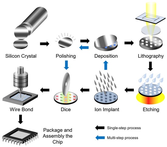
Figure 5.
Semiconductor manufacturing process flow.
In addition to optimization, substituting gases with high global warming potentials with lower-impact alternatives is an effective mitigation strategy [66,70]. C2F6 chamber cleaning technology, a widely used CVD process, involves the decomposition of inert fluorocarbon gases in the plasma region, releasing active fluorine species that react to vaporize silicon residues into compounds such as SiF4, with the non-reactive and non-toxic nature of fluorocarbon compounds providing significant safety and handling advantages [71]. However, this process may release gases such as PFCs, which could have an impact on climate change. By optimizing the chamber cleaning process, PFC emissions can be reduced. Using C4F8 as an alternative cleaning gas is a viable solution, as it significantly reduces the amount of gas required. The combination of the low flow rates and high utilization efficiency of C4F8 helps minimize total PFC emissions while also lowering gas consumption and, ultimately, costs [72]. Although substituting high-GWP gases with low-GWP substitutes is preferable, it is often impractical in numerous plasma etching processes [73,74]. Therefore, when assessing alternative chemicals, it is crucial to consider more than just their environmental impact. A thorough evaluation must include safety and health risks related to factory operations, employee protection, and the surrounding environment. This systemic method guarantees that the selected alternatives successfully cut GHG emissions, meet safety regulations, and support the long-term health and stability of the semiconductor manufacturing ecosystem [68]. Developing more sustainable CVD processes is vital, while ensuring no adverse effects on the performance of deposited films.
Advancements in lithography technologies also present significant sustainability opportunities. Extreme ultraviolet (EUV) lithography, now gaining traction in advanced chip production, allows for smaller transistors with fewer process steps, reducing material use and energy consumption [75]. Although EUV equipment involves substantial initial investments, it significantly reduces the multiple exposures, reticle requirements, and processing steps traditionally needed with longer-wavelength lithography. These operational advantages translate into considerable long-term reductions in production time, costs, and material consumption, making EUV lithography a critical technology for achieving low-carbon and cost-effective semiconductor manufacturing [76,77]. As EUV technology becomes increasingly widespread, it is expected to offer semiconductor manufacturers more energy-efficient and effective solutions in the years ahead [78]. Adopting advanced emission reduction systems offers an innovative solution for cutting GHG emissions in the semiconductor industry, significantly reducing FC and N2O emissions [46]. Additionally, remote plasma cleaning has shown to be an effective and sustainable method for removing residual materials from CVD chambers after deposition [79]. Polymer brushes and BCP photolithography technologies hold significant potential for industrial semiconductor manufacturing [80]. These lithography techniques have the potential to provide cost-effective and environmentally sustainable alternatives to conventional nanomanufacturing processes.
Beyond fabrication, design innovations in low-power integrated circuits are helping to reduce the energy consumption of semiconductor devices themselves. Techniques such as dynamic voltage scaling and power gating are increasingly used to maintain performance while lowering operational energy use [81,82]. These strategies contribute to the growing field of “green semiconductors”, which aim to reduce the lifecycle environmental footprint of electronic products [83,84]. Furthermore, waste heat recovery and reuse technologies have become widely adopted in the semiconductor industry [85,86]. High-temperature equipment and processes in semiconductor manufacturing produce considerable amounts of waste heat, which is often released into the environment, leading to significant energy waste [87,88]. Recently, some prominent semiconductor manufacturers have begun implementing waste heat recovery systems, converting excess heat from production into usable energy for heating or other manufacturing processes [89,90,91]. By recovering this waste heat, companies can notably cut energy costs and decrease carbon dioxide emissions.
3.2. Clean Energy and Energy Efficiency
Beyond production-level improvements, transitioning to low-carbon energy sources and enhancing energy efficiency are essential levers for achieving medium- to long-term emissions reduction goals. As a key industrial sector, the semiconductor industry must prioritize the adoption of clean energy solutions and enhance energy efficiency throughout its production processes to achieve future decarbonization goals [92]. Currently, most semiconductor manufacturing relies on traditional energy, particularly in regions where fossil fuels are the dominant energy source. Numerous studies have highlighted that carbon emissions from energy consumption are a major contributor to the semiconductor industry’s GHG emissions [36,93,94,95]. As a result, an increasing number of studies have focused on integrating clean energy solutions and developing energy-efficient technologies to reduce the environmental impact of energy-related emissions within the sector.
The shift to renewable energy is a key trend in the semiconductor industry. As climate change intensifies, manufacturers are gradually replacing fossil fuels with cleaner alternatives such as solar, wind, and hydropower. China’s non-fossil power share rose to over one-third by 2024, with coal’s share falling below 60% [96]. In the United States, wind and solar power are expected to account for 18% of electricity generation, with coal’s share declining to 17% [97]. Japan and South Korea have also raised their clean power output while curbing coal use [98,99]. This shift will reduce Scope 2 GHG emissions and lower long-term operational costs, supporting both environmental and economic sustainability [100,101]. Major manufacturers are responding through green power purchases and RE100 commitments. For instance, industry leaders such as the TSMC and Intel have committed to running their manufacturing plants entirely on renewable energy [102,103]. By incorporating renewable energy into their operations, semiconductor manufacturers can reduce dependence on carbon-intensive power grids, ultimately lowering their overall carbon footprint. Furthermore, adopting renewable energy enhances a company’s sustainability profile, attracting environmentally conscious investors and consumers. Furthermore, energy efficiency has become a primary focus in the semiconductor industry. As demand for more advanced and smaller chips grows, the industry is increasingly innovating to optimize energy use in manufacturing processes. Semiconductor production requires precise control of environmental factors such as temperature and pressure, which are typically energy-intensive [104,105]. To improve energy efficiency, semiconductor companies have invested heavily in energy-saving technologies. Many companies are now utilizing advanced cooling systems to reduce the energy required to maintain optimal operating conditions [106]. Some studies indicate that liquid cooling systems and advanced heat exchangers are being increasingly deployed to minimize energy consumption during manufacturing [101,107,108].
Smart manufacturing has become a crucial strategy for optimizing energy use. By utilizing artificial intelligence (AI) and the IoT, manufacturers can track production processes and energy consumption in real time [109,110,111]. AI-powered systems are capable of predicting energy usage, identifying inefficiencies, and providing real-time optimization recommendations, ensuring more efficient energy use and minimizing waste [112,113]. The TSMC has leveraged artificial intelligence to improve energy efficiency across its facilities, developing an AI-driven chiller system optimization platform that achieved a reduction of approximately 1000 tons of CO2 emissions [114]. These smart systems not only enhance energy efficiency but also improve flexibility in managing variable energy demands, further reducing the environmental footprint of semiconductor production [115,116]. Energy recovery technologies are also crucial for improving energy efficiency. Semiconductor manufacturing produces significant waste heat, which can be recovered and reused [117,118]. Advanced heat recovery systems enable manufacturers to convert waste heat into usable energy, decreasing reliance on external energy sources [118,119].
3.3. Supply Chain Management and Optimization
Supply chain management and optimization are crucial for carbon reduction in the semiconductor industry. The supply chain spans multiple stages, from raw material procurement to product delivery, with emissions generated at each step. Due to the complexity and multi-tiered nature of the supply chain, effectively reducing its carbon footprint requires comprehensive optimization from upstream to downstream, particularly in green procurement, logistics optimization, and intelligent supply chain management.
Green procurement is a critical aspect of semiconductor supply chain optimization. Semiconductor manufacturing relies heavily on rare earth metals and chemicals, with traditional extraction and transportation processes often linked to GHG emissions [42,120]. Consequently, more semiconductor companies are partnering with suppliers to encourage the use of low-carbon materials [121]. For instance, the sourcing of silicon materials and rare earth metals is gradually shifting from traditional mining to more environmentally friendly recycling and reuse practices, effectively reducing carbon emissions from resource extraction [122,123,124]. Additionally, semiconductor manufacturers are implementing green procurement policies, requiring suppliers to adopt renewable energy and provide low-carbon production solutions, thereby reducing the GHG emissions of the supply chain from source [125,126,127]. In this way, semiconductor companies can not only ensure a more sustainable and green supply chain but also raise environmental standards across the entire supply chain.
Logistics optimization is crucial in the semiconductor supply chain, which often involves international transportation. The associated GHG emissions are significant and should not be overlooked. As the semiconductor sector continues to expand globally, energy consumption and carbon emissions during transportation have become key drivers of the overall carbon footprint. Semiconductor companies are therefore increasingly prioritizing logistics optimization by adopting more efficient transportation modes, such as electric trucks and low-carbon shipping, substantially reducing transit-related carbon emissions [128,129]. Recent studies further highlight the importance of incorporating carbon emission taxation policies into logistics models, demonstrating that such integration can effectively optimize vehicle routing and selection, thereby reducing greenhouse gas emissions throughout the supply chain [130]. Moreover, adopting stochastic planning models that consider environmental factors and potential future risks can enhance decision-making robustness in locating product collection centers, ultimately supporting sustainable supply chain management practices [131]. Additionally, optimizing transportation routes to minimize unnecessary air freight and empty-haul transport through precise logistics data analysis helps companies streamline delivery schedules and reduce energy waste [132,133]. Overall, logistics optimization not only reduces operational costs but also significantly lowers transportation-related carbon emissions, positioning it as a critical strategy for decreasing the supply chain’s carbon footprints [134,135].
Smart supply chain management is crucial for reducing carbon emissions. By utilizing AI, the IoT, and big data analytics, semiconductor companies can effectively monitor and optimize energy usage throughout the entire supply chain [136,137]. For instance, AI can forecast raw material demand, helping to avoid unnecessary energy consumption and carbon emissions caused by overstocking or excessive production [138,139,140]. Real-time energy monitoring during production and transportation enables companies to identify high-energy-consuming areas and implement optimization measures, enhancing energy efficiency, reducing waste, and ultimately lowering carbon emissions [141,142].
Accurately tracking and quantifying Scope 3 emissions is essential for advancing decarbonization across the semiconductor supply chain. An increasing number of companies are adopting carbon footprint calculation tools and environmental performance databases—such as the CDP and the GHG Protocol Supply Chain Module—to estimate indirect emission sources [143,144]. In addition, lifecycle assessment (LCA) and environmentally extended input–output (EEIO) models are widely used to evaluate embedded emissions across various stages of production [8,13,145]. Meanwhile, some leading firms are developing end-to-end carbon traceability systems, leveraging technologies such as the IoT and blockchain to facilitate real-time tracking and data sharing across the supply chain [146,147,148]. The application of these methods is highly significant for GHG emissions mitigation, as they not only help companies identify carbon-intensive processes and emission hotspots but also provide a data-driven foundation for setting science-based emissions mitigation targets.
Finally, supply chain collaboration and standardization are effective strategies for driving overall carbon reduction in the semiconductor industry. To address the challenges of global climate change, many semiconductor companies are working with upstream and downstream partners in their supply chains to set carbon reduction targets and promote green transformation within the industry. For example, the Semiconductor Industry Association (SIA) and other relevant industry organizations are establishing unified emission reduction standards and encouraging green collaboration among companies [149,150]. By sharing technologies, experiences, and best practices, all parties in the supply chain can collectively improve energy efficiency and reduce carbon emissions [151,152]. Furthermore, collaboration between semiconductor raw material suppliers and waste recovery and remanufacturing companies is essential, particularly for the high-purity recycling of chemical waste. Semiconductor manufacturing relies on various chemicals, the extraction and production of which impose significant environmental impacts and require substantial costs. However, recovering and reusing chemical waste from the production process can significantly mitigate these influences. For example, since 2018, Intel has been sending sulfuric acid wastewater from one of its factories to a third-party factory for recovery and remanufacturing into industrial-grade sulfuric acid [153]. Moreover, Intel has repurposed a portion of this treated wastewater for semiconductor production across multiple facilities [153]. By adopting this strategy, the company expects to save over USD 700,000 in waste treatment costs within three years [42,153]. Such strategies play a key role in minimizing material waste and reducing the reliance on raw materials in manufacturing processes, delivering both environmental and economic benefits. Additionally, some companies are advocating for the establishment of carbon emissions trading and reporting mechanisms within the industry, ensuring that each stage adheres to standardized environmental criteria, thus enhancing the overall sustainability of the supply chain [154,155,156,157]. This standardized collaboration not only accelerates the adoption of environmentally friendly technologies but also helps guide the semiconductor industry toward a greener, more sustainable future.
4. Conclusions
Decarbonizing the semiconductor industry is an urgent and multifaceted challenge that demands coordinated, systemic solutions. This review has explored the industry’s broad environmental footprint, including greenhouse gas emissions, air and water pollution, and solid waste generation. Both front-end and back-end manufacturing processes contribute significantly to emissions, particularly through the use of fluorinated gases and high electricity consumption. In addition, upstream supply chain activities remain a major, often under-addressed, source of emissions, further complicating efforts to reduce the sector’s overall impact.
Effective mitigation requires a combination of technological innovation and process optimization. Key strategies include replacing gases with high global warming potentials, improving plasma and chemical vapor deposition techniques, advancing next-generation lithography, and deploying intelligent control systems. The adoption of renewable energy, implementation of waste heat recovery, and investments in energy efficiency have shown promising results, especially in lowering Scope 2 emissions. Similarly, chemical recycling and material recovery present viable pathways for reducing resource use and environmental harm. However, barriers such as high capital costs, technological limitations, and regional disparities continue to restrict the widespread adoption of these solutions.
Addressing emissions across the supply chain calls for a broader, system-level perspective. Measures such as green procurement, optimized logistics, and supplier collaboration are essential to support decarbonization beyond production facilities. However, the global and highly fragmented nature of the semiconductor supply network poses challenges to standardizing and scaling these efforts. While some industry leaders have taken proactive steps, such as sourcing renewable energy and embracing circular economy principles, sector-wide progress will require more robust regulatory frameworks, shared environmental standards, and coordinated action across regions and tiers.
Ultimately, technological progress alone will not be sufficient. A successful transition demands collaborative engagement from all stakeholders, including manufacturers, suppliers, policymakers, and researchers. Policies that incentivize low-carbon innovation must be coupled with mechanisms that promote transparency, data sharing, and the adoption of consistent performance metrics. Emerging digital technologies, particularly artificial intelligence and real-time emissions monitoring, can further support these efforts by enabling more precise control, informed decision-making, and streamlined emissions tracking throughout the semiconductor lifecycle.
5. Future Perspectives
While recent advancements have contributed to decarbonization efforts in the semiconductor industry, significant gaps remain that require further research and action. Current mitigation technologies and strategies are often limited to isolated production processes and are not yet integrated across the entire value chain. Differences in manufacturing techniques, material requirements, and equipment configurations hinder the scalability of existing solutions. High capital costs and the inertia of legacy infrastructure further discourage companies from transitioning to advanced, low-emission technologies. Moreover, although some overlap exists between the sources of greenhouse gas emissions and air pollutants, few studies have explored how to address both simultaneously. Most efforts remain fragmented, lacking a coordinated, system-level approach that spans the full lifecycle of semiconductor products.
Research to date has largely concentrated on process gas optimization and energy efficiency, with less attention given to supply chain emissions, material reuse, and waste recycling. While significant progress has been made in certain production stages with technologies such as material substitution, clean energy adoption, and waste heat recovery, these solutions have yet to be widely implemented across the entire production system, particularly in establishing a green supply chain to achieve system-wide decarbonization goals. Due to the complexity and multi-tier nature of the semiconductor supply chain, the lack of standardized emission mitigation frameworks across different suppliers makes it challenging for individual companies to meet decarbonization targets. A notable example of chemical waste recovery is its repurposing for other industries, with existing solutions often redirecting recovered chemicals, such as ammonium sulfate byproducts, for fertilizer production. However, if reprocessing technologies for chemical waste could achieve the high-purity standards required for semiconductor manufacturing, semiconductor producers could incorporate a greater proportion of recycled chemicals into their processes, further reducing production costs while minimizing environmental impacts. Achieving this requires not only more advanced waste recovery and reprocessing technologies but also close collaboration between chemical waste recyclers, remanufacturers, and raw material suppliers. Many studies emphasize that supply chain emissions contribute the most to the overall carbon footprint [13,47,80,158], yet few companies have taken steps to reduce emissions within their supply chains, and even those have primarily focused on energy efficiency. While reducing Scope 2 emissions from suppliers can help achieve short-term mitigation goals, long-term strategies are needed to further address emissions from supplier production processes and transportation.
Moreover, although some leading companies such as the TSMC, Intel, and Apple have committed to fully relying on renewable energy for their manufacturing processes, there is still insufficient policy support and a lack of industry standards to promote the global adoption of this practice. The differences in energy policies between countries and regions, especially in developing countries where renewable energy adoption is limited, pose challenges to achieving balanced decarbonization across the global semiconductor industry. Addressing this challenge requires stronger industry collaboration and guidance from policymakers. It is also worth noting that regional differences exist in the semiconductor industry’s decarbonization efforts, as various countries and regions play distinct roles across different stages of the semiconductor lifecycle (Figure 6). For instance, the United States, with its strong leadership in semiconductor design, bears the primary responsibility of developing more sustainable chips. Meanwhile, China (including Taiwan), as the world’s largest center for semiconductor manufacturing, is expected to focus its decarbonization efforts on mitigating GHG emissions in production processes. Governments and local enterprises should adapt their emission mitigation strategies to align with the specific characteristics of their semiconductor industries. This presents both challenges and opportunities. The challenge lies in accurately identifying the primary emission sources within different regions, ensuring that mitigation efforts are effectively targeted. On the other hand, the opportunity lies in the ability to implement lifecycle-specific emission mitigation strategies, which can achieve substantial environmental benefits at lower costs. By adopting regionally optimized approaches, certain areas may achieve a more rapid and cost-effective transition toward sustainability in the semiconductor industry. Furthermore, intense cross-border competition tends to drive production costs and product pricing to their lowest possible levels, inadvertently discouraging investments in recovery, repurification, and sustainable production practices. Therefore, achieving sustainability in semiconductor manufacturing and recycling through technological innovation and process optimization urgently requires stronger international coordination and global policy agreements.
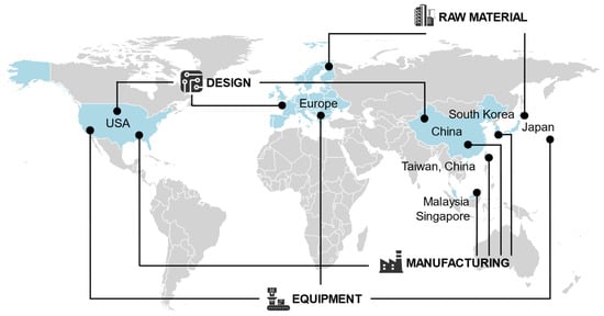
Figure 6.
Key regions for semiconductor design, raw materials, equipment, and manufacturing.
Future studies should focus on achieving green transformation across the entire value chain of the semiconductor industry. Semiconductor factories need to further apply advanced clean production technologies, and developing more cost-effective alternatives should be a key research focus to minimize the additional emissions and costs associated with process upgrades. Additionally, further exploration is needed on how to integrate clean energy and energy optimization technologies while accelerating the transition of semiconductor factories’ power systems to renewable energy sources. In the short term, while additional emissions from new renewable energy generation facilities are inevitable, achieving zero emissions in electricity-related emissions is the most achievable goal in the near future compared to reducing process gases and supply chain emissions. Moreover, the integration of smart manufacturing and artificial intelligence technologies will be crucial for mitigating environmental impacts. This approach offers multiple benefits. First, real-time emissions monitoring at the production level enables precise control of GHG emissions and pollutant leaks. Second, intelligent control systems can optimize energy efficiency in production equipment and facilities, ensuring more accurate management of energy consumption. Third, building an intelligent supply chain will enable semiconductor companies to clearly track emissions from each supplier. Fourth, water and solid waste management in semiconductor production can be automated through smart systems, enabling efficient sorting, recycling, and reuse, further reducing waste resources while shortening the recycling process, with both environmental and economic benefits.
A comprehensive transition toward sustainability in the semiconductor industry requires not only technological innovation but also active collaboration across the entire value chain. A call to action is urgently needed for all stakeholders—including manufacturers, suppliers, policymakers, and researchers—to collectively pursue more integrated and coordinated decarbonization strategies. Given the complex and globalized nature of semiconductor production, isolated efforts are insufficient to achieve meaningful progress. Upstream suppliers must work closely with downstream manufacturers to implement low-carbon materials and cleaner production techniques, while policymakers should provide regulatory incentives and frameworks that support these collaborations. Research institutions and industry associations can facilitate the sharing of best practices, data transparency, and standardized environmental metrics to ensure that sustainability efforts are aligned across regions and sectors. Moreover, the integration of digital tools, such as AI-based emissions monitoring and intelligent supply chain platforms, can enable more precise decision-making and optimize emissions reductions at each stage of production. By fostering systemic cooperation and shared responsibility, the industry can overcome fragmentation and accelerate the development and adoption of scalable low-carbon solutions. Such collective action is essential to reduce the environmental footprint of semiconductors while maintaining their vital role in driving technological progress and global economic growth.
Furthermore, future research should further explore the differences in cost-effectiveness and scalability across various decarbonization strategies. Although multiple technological pathways, such as process optimization, material substitution, clean energy substitution, and smart manufacturing, have been proposed, their implementation costs, levels of technological maturity, and scalability vary significantly across countries and enterprises. The absence of a unified assessment framework and the limited availability of transparent data currently hinder the development of a comprehensive cost–scalability comparison matrix. Therefore, there is an urgent need for evidence-based comparative studies to evaluate the economic viability and large-scale applicability of different mitigation technologies under real-world conditions, especially in regions with limited resources or insufficient policy support. Developing regionally adaptive and economically viable decarbonization pathways will help guide a differentiated and phased green transition across the semiconductor sector. We recommend that future policies and industrial research place greater emphasis on systematic assessments in this area to support more precise and context-specific emission reduction strategies.
Finally, policy support and industry standards are essential. Governments and international organizations should establish stricter emission standards and environmental regulations to encourage semiconductor companies to adopt cleaner technologies and reduce GHG emissions in production. By offering incentives and subsidies, governments can drive investment in green technologies and clean energy. In addition, collaboration and information sharing within the industries are crucial. Industry associations, standardization organizations, and research institutions should strengthen cooperation to develop environmental standards for the semiconductor industry, ensuring that green transformation is implemented across the entire value chain. Furthermore, semiconductor companies should foster collaboration with upstream and downstream suppliers to collectively advance emissions mitigation efforts. To meet global decarbonization goals, transparent supply chain management systems must be established, enabling companies to accurately assess and reduce GHG emissions at each stage. While the semiconductor industry’s path to zero emissions presents significant challenges, it also holds considerable potential for emissions mitigation. Although there may be short-term costs and technical barriers, the long-term green transformation of the semiconductor industry will not only mitigate environmental impacts but also enhance competitiveness and economic benefits for companies. Therefore, the decarbonization of the semiconductor industry is not only a critical response to climate change but also a vital step toward advancing global sustainable development.
Author Contributions
Conceptualization, Y.Y. (Yi Yang); writing—original draft preparation, Y.Y. (Yilong Yin); writing—review and editing, Y.Y. (Yilong Yin) and Y.Y. (Yi Yang); visualization, Y.Y. (Yilong Yin); supervision, Y.Y. (Yi Yang). All authors have read and agreed to the published version of the manuscript.
Funding
This research received no external funding.
Institutional Review Board Statement
Not applicable.
Informed Consent Statement
Not applicable.
Data Availability Statement
No new data were created or analyzed in this study. Data sharing is not applicable to this article.
Conflicts of Interest
The authors declare no conflicts of interest.
Abbreviations
The following abbreviations are used in this manuscript:
| AI | Artificial Intelligence |
| USD | US Dollar |
| GHG | Greenhouse Gas |
| PFCs | Perfluorocarbons |
| HFCs | Hydrofluorocarbons |
| NF3 | Nitrogen Trifluoride |
| SF6 | Sulfur Hexafluoride |
| CO2 | Carbon Dioxide |
| IoT | Internet of Things |
| 5G | Fifth generation |
| GWP | Global Warming Potential |
| VOCs | Volatile Organic Compounds |
| NOx | Nitrogen Oxides |
| SOx | Sulfur Oxides |
| PM | Particulate Matter |
| BEOL | Back end of the line |
| FEOL | Front end of the line |
| CVD | Chemical Vapor Deposition |
| CMP | Chemical Mechanical Polishing |
| BGA | Ball Grid Array |
| FC | Flip-Chip |
| LF | Lead Frame |
| H2SO4 | Sulfuric Acid |
| HF | Hydrofluoric Acid |
| HCl | Hydrochloric Acid |
| HNO3 | Nitric Acid |
| TSMC | Taiwan Semiconductor Manufacturing Company |
| UPW | Ultrapure water |
| Si | Silicon |
| GaAs | Gallium Arsenide |
| CdTe | Cadmium Telluride |
| GaN | Gallium Nitride |
| PFAS | Per- and Polyfluoroalkyl Substances |
| E-waste | Electronic Waste |
| DRAM | Dynamic Random Access Memory |
| C4F8 | Octafluorocyclobutane |
| EUV | Extreme ultraviolet |
| N2O | Nitrous Oxide |
| BCP | Block Copolymer |
| CCS | Carbon Capture and Storage |
| ALD | Atomic Layer Deposition |
| SOD | Spin-On Dielectrics |
References
- Statista Semiconductors—Worldwide|Statista Market Forecast. Available online: https://www.statista.com/outlook/tmo/semiconductors/worldwide (accessed on 24 May 2024).
- McKinsey Company Semiconductors in China: Brave New World or Same Old Story?|McKinsey. Available online: https://www.mckinsey.com/industries/semiconductors/our-insights/semiconductors-in-china-brave-new-world-or-same-old-story#/ (accessed on 26 January 2025).
- Pelcat, M. GHG Emissions of Semiconductor Manufacturing in 2021. Ph.D. Thesis, University of Rennes, Rennes, France, 2023. [Google Scholar]
- Malmodin, J.; Lövehagen, N.; Bergmark, P.; Lundén, D. ICT Sector Electricity Consumption and Greenhouse Gas Emissions—2020 Outcome. Telecommun. Policy 2024, 48, 102701. [Google Scholar] [CrossRef]
- Ruberti, M. The Chip Manufacturing Industry: Environmental Impacts and Eco-Efficiency Analysis. Sci. Total Environ. 2023, 858, 159873. [Google Scholar] [CrossRef] [PubMed]
- SEMI. Semiconductor Climate Consortium; BCG. A White Paper on Transparency, Ambition, and Collaboration. Available online: https://discover.semi.org/transparency-ambition-and-collaboration-white-paper-download-registration.html (accessed on 23 January 2025).
- Richard, C. Semiconductor Manufacturing. In Understanding Semiconductors: A Technical Guide for Non-Technical People; Richard, C., Ed.; Apress: Berkeley, CA, USA, 2023; pp. 57–80. ISBN 978-1-4842-8847-4. [Google Scholar]
- Vauche, L.; Guillemaud, G.; Lopes Barbosa, J.-C.; Di Cioccio, L. Cradle-to-Gate Life Cycle Assessment (LCA) of GaN Power Semiconductor Device. Sustainability 2024, 16, 901. [Google Scholar] [CrossRef]
- Tsai, W.-T.; Tsai, C.-H. A Survey on Fluorinated Greenhouse Gases in Taiwan: Emission Trends, Regulatory Strategies, and Abatement Technologies. Environments 2023, 10, 113. [Google Scholar] [CrossRef]
- Statista TSMC: Volume of Scope 1 GHG Emissions by Emitter. 2023. Available online: https://www.statista.com/statistics/1312928/tsmc-volume-of-scope-1-ghg-emissions-by-emitter/ (accessed on 24 January 2025).
- Statista TSMC: Volume of Scope 2 GHG Emissions by Emitter. 2023. Available online: https://www.statista.com/statistics/1312938/tsmc-volume-of-scope-2-ghg-emissions-by-emitter/ (accessed on 24 January 2025).
- Statista TSMC: Volume of Scope 3 GHG Emissions by Origin. 2022. Available online: https://www.statista.com/statistics/1312955/tsmc-volume-of-scope-3-ghg-emissions-by-origin/ (accessed on 24 January 2025).
- Kuo, T.-C.; Kuo, C.-Y.; Chen, L.-W. Assessing Environmental Impacts of Nanoscale Semi-Conductor Manufacturing from the Life Cycle Assessment Perspective. Resour. Conserv. Recycl. 2022, 182, 106289. [Google Scholar] [CrossRef]
- Li, T.; Hou, J.; Yan, J.; Liu, R.; Yang, H.; Sun, Z. Chiplet Heterogeneous Integration Technology—Status and Challenges. Electronics 2020, 9, 670. [Google Scholar] [CrossRef]
- Maitra, V.; Su, Y.; Shi, J. Virtual Metrology in Semiconductor Manufacturing: Current Status and Future Prospects. Expert Syst. Appl. 2024, 249, 123559. [Google Scholar] [CrossRef]
- Liu, C.H.; Lin, S.J.; Lewis, C. Life Cycle Assessment of DRAM in Taiwan’s Semiconductor Industry. J. Clean. Prod. 2010, 18, 419–425. [Google Scholar] [CrossRef]
- Kuo, C.-H.; Hu, A.H.; Hung, L.H.; Yang, K.-T.; Wu, C.-H. Life Cycle Impact Assessment of Semiconductor Packaging Technologies with Emphasis on Ball Grid Array. J. Clean. Prod. 2020, 276, 124301. [Google Scholar] [CrossRef]
- Alim, M.A.; Abdullah, M.Z.; Aziz, M.S.A.; Kamarudin, R. Die Attachment, Wire Bonding, and Encapsulation Process in LED Packaging: A Review. Sens. Actuators A Phys. 2021, 329, 112817. [Google Scholar] [CrossRef]
- Nguyen, M.T.N.; Lee, J.S. Development of a Chemical Sensor Device for Monitoring Hazardous Gases Generated in the Semiconductor Manufacturing Process. Chemosensors 2024, 12, 233. [Google Scholar] [CrossRef]
- Zhang, H.; Dai, L.; Feng, Y.; Xu, Y.; Liu, Y.; Guo, G.; Dai, H.; Wang, C.; Wang, C.; Hsi, H.-C.; et al. A Resource Utilization Method for Volatile Organic Compounds Emission from the Semiconductor Industry: Selective Catalytic Oxidation of Isopropanol to Acetone Over Au/α-Fe2O3 Nanosheets. Appl. Catal. B Environ. 2020, 275, 119011. [Google Scholar] [CrossRef]
- Hsieh, S.; Lin, P.-Y.; Lin, I.-H.; Beck, D.E.; Lin, C.-H. Assessing the Contribution of Semiconductors to the Sustainable Development Goals (SDGs) from 2017 to 2022. Heliyon 2023, 9, e21306. [Google Scholar] [CrossRef] [PubMed]
- Liu, W.; Fang, J.; Liang, Y.; Wang, X.; Zhang, Q.; Wang, J.; He, M.; Wang, W.; Deng, J.; Ren, C.; et al. Acid Rain Reduced Soil Carbon Emissions and Increased the Temperature Sensitivity of Soil Respiration: A Comprehensive Meta-Analysis. Sci. Total Environ. 2024, 923, 171370. [Google Scholar] [CrossRef]
- Kok, J.F.; Storelvmo, T.; Karydis, V.A.; Adebiyi, A.A.; Mahowald, N.M.; Evan, A.T.; He, C.; Leung, D.M. Mineral Dust Aerosol Impacts on Global Climate and Climate Change. Nat. Rev. Earth Environ. 2023, 4, 71–86. [Google Scholar] [CrossRef]
- Schraufnagel, D.E. The Health Effects of Ultrafine Particles. Exp. Mol. Med. 2020, 52, 311–317. [Google Scholar] [CrossRef]
- Ali, M.U.; Liu, G.; Yousaf, B.; Ullah, H.; Abbas, Q.; Munir, M.A.M. A Systematic Review on Global Pollution Status of Particulate Matter-Associated Potential Toxic Elements and Health Perspectives in Urban Environment. Environ. Geochem. Health 2019, 41, 1131–1162. [Google Scholar] [CrossRef]
- Zhou, Q.; Chen, J.; Zhang, J.; Zhou, F.; Zhao, J.; Wei, X.; Zheng, K.; Wu, J.; Li, B.; Pan, B. Toxicity and Endocrine-Disrupting Potential of PM2.5: Association with Particulate Polycyclic Aromatic Hydrocarbons, Phthalate Esters, and Heavy Metals. Environ. Pollut. 2022, 292, 118349. [Google Scholar] [CrossRef]
- Lu, H.-H.; Lu, M.-C.; Le, T.-C.; An, Z.; Pui, D.Y.H.; Tsai, C.-J. Continuous Improvements and Future Challenges of Air Pollution Control at an Advanced Semiconductor Fab. Aerosol Air Qual. Res. 2023, 23, 230034. [Google Scholar] [CrossRef]
- Villard, A.; Lelah, A.; Brissaud, D. Drawing a Chip Environmental Profile: Environmental Indicators for the Semiconductor Industry. J. Clean. Prod. 2015, 86, 98–109. [Google Scholar] [CrossRef]
- Mai, J.-L.; Cai, X.-C.; Luo, D.-Y.; Zeng, Y.; Guan, Y.-F.; Gao, W.; Chen, S.-J. Spatiotemporal Variations, Sources, and Atmospheric Transformation Potential of Volatile Organic Compounds in an Industrial Zone Based on High-Resolution Measurements in Three Plants. Sci. Total Environ. 2024, 923, 171352. [Google Scholar] [CrossRef]
- TSMC. Resources: Sustainability Reports and Documents—TSMC Corporate Social Responsibility. Available online: https://esg.tsmc.com/en/resources/documents.html (accessed on 25 January 2025).
- TSMC. TSMC ESG—TSMC Leads the Industry to Develop Dual-Rotor Zeolite Concentrators. Reduction Rate of Volatile Organic Gas Emissions Achieves 99.5%. Available online: https://esg.tsmc.com/en-US/articles/31 (accessed on 26 March 2025).
- TSMC. TSMC ESG—TSMC Optimizes Air Pollution Control Equipment, Reducing Nitrogen Oxide Emissions by 65%. Available online: https://esg.tsmc.com/en-US/articles/272 (accessed on 26 March 2025).
- Boyd, S.B. Life-Cycle Assessment of Semiconductors; Springer Science & Business Media: Berlin/Heidelberg, Germany, 2011; ISBN 978-1-4419-9988-7. [Google Scholar]
- Den, W.; Chen, C.-H.; Luo, Y.-C. Revisiting the Water-Use Efficiency Performance for Microelectronics Manufacturing Facilities: Using Taiwan’s Science Parks as a Case Study. Water-Energy Nexus 2018, 1, 116–133. [Google Scholar] [CrossRef]
- Frost, K.; Hua, I. Quantifying Spatiotemporal Impacts of the Interaction of Water Scarcity and Water Use by the Global Semiconductor Manufacturing Industry. Water Resour. Ind. 2019, 22, 100115. [Google Scholar] [CrossRef]
- Wang, Q.; Huang, N.; Chen, Z.; Chen, X.; Cai, H.; Wu, Y. Environmental Data and Facts in the Semiconductor Manufacturing Industry: An Unexpected High Water and Energy Consumption Situation. Water Cycle 2023, 4, 47–54. [Google Scholar] [CrossRef]
- TSMC. TSMC Arizona and U.S. Department of Commerce Announce Up to US$6.6 Billion in Proposed CHIPS Act Direct Funding, the Company Plans Third Leading-Edge Fab in Phoenix. Available online: https://pr.tsmc.com/schinese/news/3122 (accessed on 26 March 2025).
- Intel. Intel and the Environment—Water Restoration in Arizona. Available online: https://www.intel.com/content/www/us/en/environment/water-restoration-arizona.html (accessed on 26 March 2025).
- Team S.E. Samsung Semiconductor Will Use Wastewater for Chip Production. Available online: https://smartwatermagazine.com/news/smart-water-magazine/samsung-semiconductor-will-use-wastewater-chip-production (accessed on 26 March 2025).
- NIST Waste Management in Semiconductor Facilities. Available online: https://www.nist.gov/chips/chips-incentives-funding-opportunities/environmental-division/waste-management-semiconductor (accessed on 25 January 2025).
- Platzer, M.D.; Sargent, J.F. US Semiconductor Manufacturing: Industry Trends, Global Competition, Federal Policy; Congressional Research Service: New York, NY, USA, 2016.
- Kumar, A.; Thorbole, A.; Gupta, R.K. Sustaining the Future: Semiconductor Materials and Their Recovery. Mater. Sci. Semicond. Process. 2025, 185, 108943. [Google Scholar] [CrossRef]
- Forti, V.; Balde, C.P.; Kuehr, R.; Bel, G. The Global E-Waste Monitor 2020: Quantities, Flows and the Circular Economy Potential; United Nations University/United Nations Institute for Training and Research, International Telecommunication Union, and International Solid Waste Association: Bonn, Germany; Geneva, Switzerland; Rotterdam, The Netherlands, 2020; ISBN 9789280891140. [Google Scholar]
- Apple. Apple Commits to Be 100 Percent Carbon Neutral for Its Supply Chain and Products by 2030. Available online: https://www.apple.com/newsroom/2020/07/apple-commits-to-be-100-percent-carbon-neutral-for-its-supply-chain-and-products-by-2030/ (accessed on 10 June 2024).
- Zhang, X.; Xiao, H.; Hu, X.; Zhang, Y. Effects of Reduced Electric Field on Sulfur Hexafluoride Removal for a Double Dielectric Barrier Discharge Reactor. IEEE Trans. Plasma Sci. 2018, 46, 563–570. [Google Scholar] [CrossRef]
- Zhou, Y.; Li, Y.; Ong, E. Advancements in Greenhouse Gas Emission Reduction Methodology for Fluorinated Compounds and N2O in the Semiconductor Industry via Abatement Systems. Front. Energy Res. 2024, 11, 1234486. [Google Scholar] [CrossRef]
- Nagapurkar, P.; Nandy, P.; Nimbalkar, S. Cleaner Chips: Decarbonization in Semiconductor Manufacturing. Sustainability 2024, 16, 218. [Google Scholar] [CrossRef]
- Shin, D.; Kim, J.; Lee, C.S. Evaluation of V2O5 Film-Based Electrochromic Device with Dry-Deposited Ion Storage Layer. Int. J. Precis. Eng. Manuf. 2023, 24, 119–128. [Google Scholar] [CrossRef]
- Lee, Y.; Seo, S.; Oh, I.-K.; Lee, S.; Kim, H. Effects of O2 Plasma Treatment on Moisture Barrier Properties of SiO2 Grown by Plasma-Enhanced Atomic Layer Deposition. Ceram. Int. 2019, 45, 17662–17668. [Google Scholar] [CrossRef]
- Baek, S.Y.; Park, J.; Koh, T.; Kim, D.; Woo, J.; Jung, J.; Park, S.J.; Lee, C.; Choi, C. Achievement of Green and Sustainable CVD Through Process, Equipment and Systematic Optimization in Semiconductor Fabrication. Int. J. Precis. Eng. Manuf.-Green Tech. 2024, 11, 1295–1316. [Google Scholar] [CrossRef]
- Zhang, Y.; Chen, A.; Kim, M.-W.; Alaei, A.; Lee, S.S. Nanoconfining Solution-Processed Organic Semiconductors for Emerging Optoelectronics. Chem. Soc. Rev. 2021, 50, 9375–9390. [Google Scholar] [CrossRef] [PubMed]
- Sharma, E.; Rathi, R.; Misharwal, J.; Sinhmar, B.; Kumari, S.; Dalal, J.; Kumar, A. Evolution in Lithography Techniques: Microlithography to Nanolithography. Nanomaterials 2022, 12, 2754. [Google Scholar] [CrossRef] [PubMed]
- Kwon, S.; Park, Y.; Ban, W.; Youn, C.; Lee, S.; Yang, J.; Jung, D.; Choi, T. Effect of Plasma Power on Properties of Hydrogenated Amorphous Silicon Carbide Hardmask Films Deposited by PECVD. Vacuum 2020, 174, 109187. [Google Scholar] [CrossRef]
- Sinioros, P.; Haidari, A.A.; Manousakis, N.; Lasithiotakis, M.; Tzoraki, O. Renovation and Reuse of Waste Electrical and Electronic Equipment in the Direction of Eco-Design. In Product Design; IntechOpen: Rijeka, Croatia, 2020. [Google Scholar]
- Rene, E.R.; Sethurajan, M.; Kumar Ponnusamy, V.; Kumar, G.; Bao Dung, T.N.; Brindhadevi, K.; Pugazhendhi, A. Electronic Waste Generation, Recycling and Resource Recovery: Technological Perspectives and Trends. J. Hazard. Mater. 2021, 416, 125664. [Google Scholar] [CrossRef]
- Hsu, E.; Barmak, K.; West, A.C.; Park, A.-H.A. Advancements in the Treatment and Processing of Electronic Waste with Sustainability: A Review of Metal Extraction and Recovery Technologies. Green Chem. 2019, 21, 919–936. [Google Scholar] [CrossRef]
- Lunardi, M.M.; Alvarez-Gaitan, J.P.; Bilbao, J.I.; Corkish, R. A Review of Recycling Processes for Photovoltaic Modules. In Solar Panels and Photovoltaic Materials; IntechOpen: Rijeka, Croatia, 2018; Volume 30. [Google Scholar]
- Bradwell, D.J.; Osswald, S.; Wei, W.; Barriga, S.A.; Ceder, G.; Sadoway, D.R. Recycling ZnTe, CdTe, and Other Compound Semiconductors by Ambipolar Electrolysis. J. Am. Chem. Soc. 2011, 133, 19971–19975. [Google Scholar] [CrossRef]
- Mishra, G.; Jha, R.; Meshram, A.; Singh, K.K. A Review on Recycling of Lithium-Ion Batteries to Recover Critical Metals. J. Environ. Chem. Eng. 2022, 10, 108534. [Google Scholar] [CrossRef]
- Bahaloo-Horeh, N.; Vakilchap, F.; Mousavi, S.M. Bio-Hydrometallurgical Methods for Recycling Spent Lithium-Ion Batteries. In Recycling of Spent Lithium-Ion Batteries: Processing Methods and Environmental Impacts; An, L., Ed.; Springer International Publishing: Cham, Switzerland, 2019; pp. 161–197. ISBN 978-3-030-31834-5. [Google Scholar]
- Zhan, L.; Xia, F.; Ye, Q.; Xiang, X.; Xie, B. Novel Recycle Technology for Recovering Rare Metals (Ga, In) from Waste Light-Emitting Diodes. J. Hazard. Mater. 2015, 299, 388–394. [Google Scholar] [CrossRef]
- Shen, C.; Tran, P.P.; Minh Ly, P.T. Chemical Waste Management in the U.S. Semiconductor Industry. Sustainability 2018, 10, 1545. [Google Scholar] [CrossRef]
- Saravanan, A.; Senthil Kumar, P.; Jeevanantham, S.; Karishma, S.; Tajsabreen, B.; Yaashikaa, P.R.; Reshma, B. Effective Water/Wastewater Treatment Methodologies for Toxic Pollutants Removal: Processes and Applications towards Sustainable Development. Chemosphere 2021, 280, 130595. [Google Scholar] [CrossRef] [PubMed]
- Rochlitz, L.; Steinberger, M.; Oechsner, R.; Weber, A.; Schmitz, S.; Schillinger, K.; Wolff, M.; Bayler, A. Second Use or Recycling of Hydrogen Waste Gas from the Semiconductor Industry—Economic Analysis and Technical Demonstration of Possible Pathways. Int. J. Hydrogen Energy 2019, 44, 17168–17184. [Google Scholar] [CrossRef]
- Nagapurkar, P.; Das, S. Economic and Embodied Energy Analysis of Integrated Circuit Manufacturing Processes. Sustain. Comput. Inform. Syst. 2022, 35, 100771. [Google Scholar] [CrossRef]
- Sovacool, B.K.; Griffiths, S.; Kim, J.; Bazilian, M. Climate Change and Industrial F-Gases: A Critical and Systematic Review of Developments, Sociotechnical Systems and Policy Options for Reducing Synthetic Greenhouse Gas Emissions. Renew. Sustain. Energy Rev. 2021, 141, 110759. [Google Scholar] [CrossRef]
- Choi, J.; Kim, B.; Im, S.; Yoo, G. Supervised Multivariate Kernel Density Estimation for Enhanced Plasma Etching Endpoint Detection. IEEE Access 2022, 10, 25580–25590. [Google Scholar] [CrossRef]
- Liang, Y.; Tan, K.; Li, Y. Implementation Principles of Optimal Control Technology for the Reduction of Greenhouse Gases in Semiconductor Industry. In E3S Web of Conferences; EDP Sciences: Ulis, France, 2023; Volume 394, p. 01031. [Google Scholar]
- Minimizing Greenhouse Gases—Samsung. Available online: https://semiconductor.samsung.com/emea/sustainability/environment/climate-action/we-are-minimizing-greenhouse-gases-until-we-hit-zero (accessed on 26 March 2025).
- Raoux, S. Fluorinated Greenhouse Gas and Net-Zero Emissions from the Electronics Industry: The Proof Is in the Pudding. Carbon Manag. 2023, 14, 2179941. [Google Scholar] [CrossRef]
- Lee, S.; Park, G.; Kim, D.; Kim, K. Analysis of Plasma and Gas Characteristics According to the Recovery Process Using a New Alternative Gas. Sci. Adv. Mater. 2024, 16, 280–285. [Google Scholar] [CrossRef]
- Allgood, C.C. Fluorinated Gases for Semiconductor Manufacture: Process Advances in Chemical Vapor Deposition Chamber Cleaning. J. Fluor. Chem. 2003, 122, 105–112. [Google Scholar] [CrossRef]
- Pedersen, H.; Barry, S.T.; Sundqvist, J. Green CVD—Toward a Sustainable Philosophy for Thin Film Deposition by Chemical Vapor Deposition. J. Vac. Sci. Technol. A 2021, 39, 051001. [Google Scholar] [CrossRef]
- Illuzzi, F.; Thewissen, H. Perfluorocompounds Emission Reduction by the Semiconductor Industry. J. Integr. Environ. Sci. 2010, 7, 201–210. [Google Scholar] [CrossRef]
- Kazazis, D.; Santaclara, J.G.; van Schoot, J.; Mochi, I.; Ekinci, Y. Extreme Ultraviolet Lithography. Nat. Rev. Methods Primers 2024, 4, 1–15. [Google Scholar] [CrossRef]
- Zhang, Y.; Yu, H.; Wang, L.; Wu, X.; He, J.; Huang, W.; Ouyang, C.; Chen, D.; Keshta, B.E. Advanced Lithography Materials: From Fundamentals to Applications. Adv. Colloid Interface Sci. 2024, 329, 103197. [Google Scholar] [CrossRef]
- Fu, N.; Liu, Y.; Ma, X.; Chen, Z. EUV Lithography: State-of-the-Art Review. J. Microelectron. Manuf. 2019, 2, 19020202. [Google Scholar] [CrossRef]
- Ober, C.K.; Käfer, F.; Yuan, C. Recent Developments in Photoresists for Extreme-Ultraviolet Lithography. Polymer 2023, 280, 126020. [Google Scholar] [CrossRef]
- Jadwiszczak, J.; Kelly, D.J.; Guo, J.; Zhou, Y.; Zhang, H. Plasma Treatment of Ultrathin Layered Semiconductors for Electronic Device Applications. ACS Appl. Electron. Mater. 2021, 3, 1505–1529. [Google Scholar] [CrossRef]
- Mullen, E.; Morris, M.A. Green Nanofabrication Opportunities in the Semiconductor Industry: A Life Cycle Perspective. Nanomaterials 2021, 11, 1085. [Google Scholar] [CrossRef] [PubMed]
- Tang, J.; Wang, Q.; Tian, J.; Li, X.; Li, N.; Peng, Y.; Li, X.; Zhao, Y.; He, C.; Wu, S.; et al. Low Power Flexible Monolayer MoS2 Integrated Circuits. Nat. Commun. 2023, 14, 3633. [Google Scholar] [CrossRef]
- Song, C.; Zhao, G.; Wu, B. Applications of Low-Power Design in Semiconductor Chips. J. Ind. Eng. Appl. Sci. 2024, 2, 54–59. [Google Scholar] [CrossRef]
- Yuvaraja, S.; Khandelwal, V.; Tang, X.; Li, X. Wide Bandgap Semiconductor-Based Integrated Circuits. Chip 2023, 2, 100072. [Google Scholar] [CrossRef]
- Peng, Y.; Cui, C.; Li, L.; Wang, Y.; Wang, Q.; Tian, J.; Huang, Z.; Huang, B.; Zhang, Y.; Li, X.; et al. Medium-Scale Flexible Integrated Circuits Based on 2D Semiconductors. Nat. Commun. 2024, 15, 10833. [Google Scholar] [CrossRef]
- Lee, A.; Naquash, A.; Lee, M.; Chaniago, Y.D.; Lim, H. Exploitation of Distillation for Energy-Efficient and Cost-Effective Environmentally Benign Process of Waste Solvents Recovery from Semiconductor Industry. Sci. Total Environ. 2022, 841, 156743. [Google Scholar] [CrossRef]
- Zhao, W.; Li, H.; Wang, S. A Generic Design Optimization Framework for Semiconductor Cleanroom Air-Conditioning Systems Integrating Heat Recovery and Free Cooling for Enhanced Energy Performance. Energy 2024, 286, 129600. [Google Scholar] [CrossRef]
- Yuan, X.; Liang, Y.; Hu, X.; Xu, Y.; Chen, Y.; Kosonen, R. Waste Heat Recoveries in Data Centers: A Review. Renew. Sustain. Energy Rev. 2023, 188, 113777. [Google Scholar] [CrossRef]
- Walden, D.S. Semiconductors in Industrial Waste Heat Collection Improvements. Ph.D. Thesis, West Texas A&M University, Canyon, TX, USA, 2021. [Google Scholar]
- Farhat, O.; Faraj, J.; Hachem, F.; Castelain, C.; Khaled, M. A Recent Review on Waste Heat Recovery Methodologies and Applications: Comprehensive Review, Critical Analysis and Potential Recommendations. Clean. Eng. Technol. 2022, 6, 100387. [Google Scholar] [CrossRef]
- Oyedepo, S.O.; Fakeye, B.A. Waste heat recovery technologies: Pathway to sustainable energy development. J. Therm. Eng. 2021, 7, 324–348. [Google Scholar] [CrossRef]
- Chen, W.-H.; Chiou, Y.-B.; Chein, R.-Y.; Uan, J.-Y.; Wang, X.-D. Power Generation of Thermoelectric Generator with Plate Fins for Recovering Low-Temperature Waste Heat. Appl. Energy 2022, 306, 118012. [Google Scholar] [CrossRef]
- Cresko, J.; Rightor, E.; Carpenter, A.; Peretti, K.; Elliott, N.; Nimbalkar, S.; Morrow, W.R., III; Hasanbeigi, A.; Hedman, B.; Supekar, S.; et al. U.S. Department of Energy’s Industrial Decarbonization Roadmap; USDOE Office of Energy Efficiency and Renewable Energy (EERE): Washington, DC, USA, 2022.
- Gallagher, E.; Ragnarsson, L.-Å.; Rolin, C. Sustainable Semiconductor Manufacturing: The Role of Lithography. IEEE Trans. Semicond. Manuf. 2024, 37, 440–444. [Google Scholar] [CrossRef]
- Pirson, T.; Delhaye, T.P.; Pip, A.G.; Le Brun, G.; Raskin, J.-P.; Bol, D. The Environmental Footprint of IC Production: Review, Analysis, and Lessons from Historical Trends. IEEE Trans. Semicond. Manuf. 2023, 36, 56–67. [Google Scholar] [CrossRef]
- Li, Y.; Wang, Y.; Chong, D.; Xu, Z.; Li, L.; Hu, Y. Carbon Taxation in Singapore’s Semiconductor Sector: A Mini-Review on GHG Emission Metrics and Reporting. Carbon Res. 2023, 2, 49. [Google Scholar] [CrossRef]
- U.S. Energy Information Administration (EIA). EIA China Increased Electricity Generation Annually from 2000 to 2020. Available online: https://www.eia.gov/todayinenergy/detail.php?id=53959 (accessed on 26 March 2025).
- U.S. Energy Information Administration (EIA). Short-Term Energy Outlook—U.S. Energy Information Administration (EIA); U.S. Energy Information Administration (EIA): Washington, DC, USA, 2025.
- U.S. Energy Information Administration (EIA). EIA Japan’s Energy Policies Aim for Increased Zero-Carbon Electricity Generation. Available online: https://www.eia.gov/todayinenergy/detail.php?id=61944 (accessed on 26 March 2025).
- Renewable Energy Institute South Korea. Low Renewable Energy Ambitions Result in High Nuclear and Fossil Power Dependencies; Renewable Energy Institute: Daejeon, Republic of Korea, 2024. [Google Scholar]
- Tang, Z.; Yang, Y.; Blaabjerg, F. Power Electronics: The Enabling Technology for Renewable Energy Integration. CSEE J. Power Energy Syst. 2022, 8, 39–52. [Google Scholar] [CrossRef]
- Liu, Y.-Z.; Lu, W.-M.; Tran, P.P.; Pham, T.A.K. Sustainable Energy and Semiconductors: A Bibliometric Investigation. Sustainability 2024, 16, 6548. [Google Scholar] [CrossRef]
- TSMC. TSMC Becomes the World’s First Semiconductor Company to Join RE100, Committed to 100% Renewable Energy Usage. Available online: https://esg.tsmc.com/en/update/greenManufacturing/caseStudy/37/index.html (accessed on 26 January 2025).
- Intel Renewable Electricity White Paper. Available online: https://www.intel.com/content/www/us/en/environment/renewable-electricity-white-paper.html (accessed on 26 January 2025).
- Lin, F.; Lin, S.-W.; Lu, W.-M. Dynamic Eco-Efficiency Evaluation of the Semiconductor Industry: A Sustainable Development Perspective. Environ. Monit. Assess. 2019, 191, 435. [Google Scholar] [CrossRef]
- Ni, H.-P.; Chong, W.O.; Chou, J.-S. Optimizing HVAC Systems for Semiconductor Fabrication: A Data-Intensive Framework for Energy Efficiency and Sustainability. J. Build. Eng. 2024, 89, 109397. [Google Scholar] [CrossRef]
- Chien, C.-F.; Chen, Y.-J.; Han, Y.-T.; Wu, Y.-C. Industry 3.5 for Optimizing Chiller Configuration for Energy Saving and an Empirical Study for Semiconductor Manufacturing. Resour. Conserv. Recycl. 2021, 168, 105247. [Google Scholar] [CrossRef]
- Chang, K.-H.; Tsai, C.-C.; Wang, C.-H.; Chen, C.-J.; Lin, C.-M. Optimizing the Energy Efficiency of Chiller Systems in the Semiconductor Industry through Big Data Analytics and an Empirical Study. J. Manuf. Syst. 2021, 60, 652–661. [Google Scholar] [CrossRef]
- Zhao, W.; Li, H.; Wang, S. Energy Performance and Energy Conservation Technologies for High-Tech Cleanrooms: State of the Art and Future Perspectives. Renew. Sustain. Energy Rev. 2023, 183, 113532. [Google Scholar] [CrossRef]
- Chen, Y.-Q.; Zhou, B.; Zhang, M.; Chen, C.-M. Using IoT Technology for Computer-Integrated Manufacturing Systems in the Semiconductor Industry. Appl. Soft Comput. 2020, 89, 106065. [Google Scholar] [CrossRef]
- Bauer, H.; Patel, M.; Veira, J. Internet of Things: Opportunities and Challenges for Semiconductor Companies; McKinsey Insights: New York, NY, USA, 2015. [Google Scholar]
- Jang, S.-W.; Kim, G.-Y. A Monitoring Method of Semiconductor Manufacturing Processes Using Internet of Things–Based Big Data Analysis. Int. J. Distrib. Sens. Netw. 2017, 13, 1550147717721810. [Google Scholar] [CrossRef]
- Nižetić, S.; Šolić, P.; López-de-Ipiña González-de-Artaza, D.; Patrono, L. Internet of Things (IoT): Opportunities, Issues and Challenges towards a Smart and Sustainable Future. J. Clean. Prod. 2020, 274, 122877. [Google Scholar] [CrossRef] [PubMed]
- Yanambaka, V.P.; Mohanty, S.P.; Kougianos, E. Making Use of Semiconductor Manufacturing Process Variations: FinFET-Based Physical Unclonable Functions for Efficient Security Integration in the IoT. Analog. Integr. Circuits Signal Process. 2017, 93, 429–441. [Google Scholar] [CrossRef]
- TSMC. TSMC ESG—Three Innovations of TSMC AI-Powered Water Chiller System Improve Energy-Efficiency. Available online: https://esg.tsmc.com/en-US/e-paper/202211 (accessed on 26 March 2025).
- Tareq, A.A.; Rana, M.J.; Mostofa, M.R.; Rahman, M.S. Impact of IoT and Embedded System on Semiconductor Industry A Case Study. Control Syst. Optim. Lett. 2024, 2, 211–216. [Google Scholar] [CrossRef]
- Li, B.; Chen, R.-S.; Liu, C.-Y. Using Intelligent Technology and Real-Time Feedback Algorithm to Improve Manufacturing Process in IoT Semiconductor Industry. J. Supercomput. 2021, 77, 4639–4658. [Google Scholar] [CrossRef]
- Fitriani, R.O.; Long, B.D.; Barma, M.C.; Riaz, M.; Sabri, M.F.M.; Said, S.M.; Saidur, R. A Review on Nanostructures of High-Temperature Thermoelectric Materials for Waste Heat Recovery. Renew. Sustain. Energy Rev. 2016, 64, 635–659. [Google Scholar] [CrossRef]
- Savani, I.; Waage, M.H.; Børset, M.; Kjelstrup, S.; Wilhelmsen, Ø. Harnessing Thermoelectric Power from Transient Heat Sources: Waste Heat Recovery from Silicon Production. Energy Convers. Manag. 2017, 138, 171–182. [Google Scholar] [CrossRef]
- Ononogbo, C.; Nwosu, E.C.; Nwakuba, N.R.; Nwaji, G.N.; Nwufo, O.C.; Chukwuezie, O.C.; Chukwu, M.M.; Anyanwu, E.E. Opportunities of Waste Heat Recovery from Various Sources: Review of Technologies and Implementation. Heliyon 2023, 9, e13590. [Google Scholar] [CrossRef] [PubMed]
- Patil, A.S.; Patil, A.V.; Dighavkar, C.G.; Adole, V.A.; Tupe, U.J. Synthesis Techniques and Applications of Rare Earth Metal Oxides Semiconductors: A Review. Chem. Phys. Lett. 2022, 796, 139555. [Google Scholar] [CrossRef]
- TSMC. TSMC ESG—TSMC’s New Business Collaboration Standards: Carbon Reduction Performance as a Key Supplier Selection Criterion. Available online: https://esg.tsmc.com/en-US/articles/340 (accessed on 26 January 2025).
- Xu, T.; Zheng, X.; Ji, B.; Xu, Z.; Bao, S.; Zhang, X.; Li, G.; Mei, J.; Li, Z. Green Recovery of Rare Earth Elements under Sustainability and Low Carbon: A Review of Current Challenges and Opportunities. Sep. Purif. Technol. 2024, 330, 125501. [Google Scholar] [CrossRef]
- Dutta, T.; Kim, K.-H.; Uchimiya, M.; Kwon, E.E.; Jeon, B.-H.; Deep, A.; Yun, S.-T. Global Demand for Rare Earth Resources and Strategies for Green Mining. Environ. Res. 2016, 150, 182–190. [Google Scholar] [CrossRef] [PubMed]
- Stratiotou Efstratiadis, V.; Michailidis, N. Sustainable Recovery, Recycle of Critical Metals and Rare Earth Elements from Waste Electric and Electronic Equipment (Circuits, Solar, Wind) and Their Reusability in Additive Manufacturing Applications: A Review. Metals 2022, 12, 794. [Google Scholar] [CrossRef]
- Hwang, B.-N.; Huang, C.-Y.; Wu, C.-H. A TOE Approach to Establish a Green Supply Chain Adoption Decision Model in the Semiconductor Industry. Sustainability 2016, 8, 168. [Google Scholar] [CrossRef]
- Lee, K.-H.; Kim, J.-W. Integrating Suppliers into Green Product Innovation Development: An Empirical Case Study in the Semiconductor Industry. Bus. Strategy Environ. 2011, 20, 527–538. [Google Scholar] [CrossRef]
- Chen, P.-K.; Ye, Y.; Wen, M.-H. Efficiency of Metaverse on the Improvement of the Green Procurement Policy of Semiconductor Supply Chain—Based on Behaviour Perspective. Resour. Policy 2023, 86, 104213. [Google Scholar] [CrossRef]
- Bui, T.-D. Assessing Sustainable Supply Chain Transparency Practices in Taiwan Semiconductor Industry: A Hierarchical Interdependence Approach. Int. J. Prod. Econ. 2024, 272, 109245. [Google Scholar] [CrossRef]
- Son, Y.; Ko, W.-J.; Ulrich, P.; Sarilmis, R.; Ehm, H. Transportation Product Carbon Footprint: A Framework for Semiconductor Supply Chain. In Proceedings of the 2024 Winter Simulation Conference (WSC), Orlando, FL, USA, 15–18 December 2024; pp. 1841–1852. [Google Scholar]
- Eslamipoor, R. An Optimization Model for Green Supply Chain by Regarding Emission Tax Rate in Incongruous Vehicles. Model. Earth Syst. Environ. 2023, 9, 227–238. [Google Scholar] [CrossRef]
- Eslamipoor, R. A Two-Stage Stochastic Planning Model for Locating Product Collection Centers in Green Logistics Networks. Clean. Logist. Supply Chain 2023, 6, 100091. [Google Scholar] [CrossRef]
- Wang, Y.; Zhang, H.; Yuan, C.; Li, X.; Jiang, Z. A Network Flow Approach to Optimal Scheduling in Supply Chain Logistics. arXiv 2024, arXiv:2411.17544. [Google Scholar]
- Hwang, B.-N.; Shen, Y.-C. Decision Making for Third Party Logistics Supplier Selection in Semiconductor Manufacturing Industry: A Nonadditive Fuzzy Integral Approach. Math. Probl. Eng. 2015, 2015, 918602. [Google Scholar] [CrossRef]
- Ullah, M. Impact of Transportation and Carbon Emissions on Reverse Channel Selection in Closed-Loop Supply Chain Management. J. Clean. Prod. 2023, 394, 136370. [Google Scholar] [CrossRef]
- Mönch, L.; Uzsoy, R.; Fowler, J.W. A Survey of Semiconductor Supply Chain Models Part I: Semiconductor Supply Chains, Strategic Network Design, and Supply Chain Simulation. Int. J. Prod. Res. 2018, 56, 4524–4545. [Google Scholar]
- Chien, C.-F.; Kuo, H.-A.; Lin, Y.-S. Smart Semiconductor Manufacturing for Pricing, Demand Planning, Capacity Portfolio and Cost for Sustainable Supply Chain Management. Int. J. Logist. Res. Appl. 2024, 27, 193–216. [Google Scholar]
- Lerman, L.V.; Benitez, G.B.; Müller, J.M.; de Sousa, P.R.; Frank, A.G. Smart Green Supply Chain Management: A Configurational Approach to Enhance Green Performance through Digital Transformation. Supply Chain Manag. Int. J. 2022, 27, 147–176. [Google Scholar] [CrossRef]
- Fore, V.; Khanna, A.; Tomar, R.; Mishra, A. Intelligent Supply Chain Management System. In Proceedings of the 2016 International Conference on Advances in Computing and Communication Engineering (ICACCE), Durban, South Africa, 28–29 November 2016; pp. 296–302. [Google Scholar]
- Evtodieva, T.E.; Chernova, D.V.; Ivanova, N.V.; Wirth, J. The Internet of Things: Possibilities of Application in Intelligent Supply Chain Management. In Digital Transformation of the Economy: Challenges, Trends and New Opportunities; Ashmarina, S., Mesquita, A., Vochozka, M., Eds.; Springer International Publishing: Cham, Switzerland, 2020; pp. 395–403. [Google Scholar]
- Yan, J.; Xin, S.; Liu, Q.; Xu, W.; Yang, L.; Fan, L.; Chen, B.; Wang, Q. Intelligent Supply Chain Integration and Management Based on Cloud of Things. Int. J. Distrib. Sens. Netw. 2014, 10, 624839. [Google Scholar] [CrossRef]
- Wu, L.; Yue, X.; Jin, A.; Yen, D.C. Smart Supply Chain Management: A Review and Implications for Future Research. Int. J. Logist. Manag. 2016, 27, 395–417. [Google Scholar] [CrossRef]
- Pournader, M.; Ghaderi, H.; Hassanzadegan, A.; Fahimnia, B. Artificial Intelligence Applications in Supply Chain Management. Int. J. Prod. Econ. 2021, 241, 108250. [Google Scholar] [CrossRef]
- Blanco, C.; Caro, F.; Corbett, C.J. The State of Supply Chain Carbon Footprinting: Analysis of CDP Disclosures by US Firms. J. Clean. Prod. 2016, 135, 1189–1197. [Google Scholar] [CrossRef]
- Blanco, C.C. Supply Chain Carbon Footprinting and Climate Change Disclosures of Global Firms. Prod. Oper. Manag. 2021, 30, 3143–3160. [Google Scholar] [CrossRef]
- Yang, Y.; Park, Y.; Smith, T.M.; Kim, T.; Park, H.-S. High-Resolution Environmentally Extended Input–Output Model to Assess the Greenhouse Gas Impact of Electronics in South Korea. Environ. Sci. Technol. 2022, 56, 2107–2114. [Google Scholar] [CrossRef] [PubMed]
- Rejeb, A.; Keogh, J.G.; Treiblmaier, H. Leveraging the Internet of Things and Blockchain Technology in Supply Chain Management. Future Internet 2019, 11, 161. [Google Scholar] [CrossRef]
- Sallam, K.; Mohamed, M.; Mohamed, A.W. Internet of Things (IoT) in Supply Chain Management: Challenges, Opportunities, and Best Practices. Sustain. Mach. Intell. J. 2023, 2, 1–32. [Google Scholar] [CrossRef]
- Rejeb, A.; Keogh, J.G.; Simske, S.J.; Stafford, T.; Treiblmaier, H. Potentials of Blockchain Technologies for Supply Chain Collaboration: A Conceptual Framework. Int. J. Logist. Manag. 2021, 32, 973–994. [Google Scholar] [CrossRef]
- SIA. SIA Comments on EPA Revisions to Subpart I of the GHG Reporting Rule. Available online: https://www.semiconductors.org/wp-content/uploads/2022/10/SIA-comments-on-EPA-revisions-to-Subpart-I-of-the-GHG-Reporting-Rule-10.5.2022.pdf (accessed on 26 January 2025).
- SIA Semiconductor PFAS Consortium. Available online: https://www.semiconductors.org/pfas/ (accessed on 26 January 2025).
- Dahlmann, F.; Roehrich, J.K. Sustainable Supply Chain Management and Partner Engagement to Manage Climate Change Information. Bus. Strategy Environ. 2019, 28, 1632–1647. [Google Scholar] [CrossRef]
- Saberi, S.; Kouhizadeh, M.; Sarkis, J.; Shen, L. Blockchain Technology and Its Relationships to Sustainable Supply Chain Management. Int. J. Prod. Res. 2019, 57, 2117–2135. [Google Scholar] [CrossRef]
- Fiehrer, K.; Esparza, A.; Burki, T.; Qian, L. Circularity in Intel’s Semiconductor Manufacturing: Recovery and Reuse; Intel: Santa Clara, CA, USA, 2019. [Google Scholar]
- Mo, J.Y. Technological Innovation and Its Impact on Carbon Emissions: Evidence from Korea Manufacturing Firms Participating Emission Trading Scheme. Technol. Anal. Strateg. Manag. 2022, 34, 47–57. [Google Scholar] [CrossRef]
- Zhang, Y.-J.; Liang, T.; Jin, Y.-L.; Shen, B. The Impact of Carbon Trading on Economic Output and Carbon Emissions Reduction in China’s Industrial Sectors. Appl. Energy 2020, 260, 114290. [Google Scholar] [CrossRef]
- Zhang, M.; Yang, W.; Zhao, Z.; Wang, S.; Huang, G.Q. Do Fairness Concerns Matter for ESG Decision-Making? Strategic Interactions in Digital Twin-Enabled Sustainable Semiconductor Supply Chain. Int. J. Prod. Econ. 2024, 276, 109370. [Google Scholar] [CrossRef]
- Ahmad, R.A.R.; Palaniappan, T.; Azmi, N.A. Environmental, social, and governance (ESG) disclosure and firms financial indicators: Analysis of semiconductor industry. Insight J. 2023, 10, 221–241. [Google Scholar]
- Nikolka, M.; Göke, S.; Burkacky, O.; Spiller, P.; Patel, M. Unlocking Net-Zero in Semiconductor Manufacturing. Nat. Rev. Electr. Eng. 2024, 1, 487–488. [Google Scholar] [CrossRef]
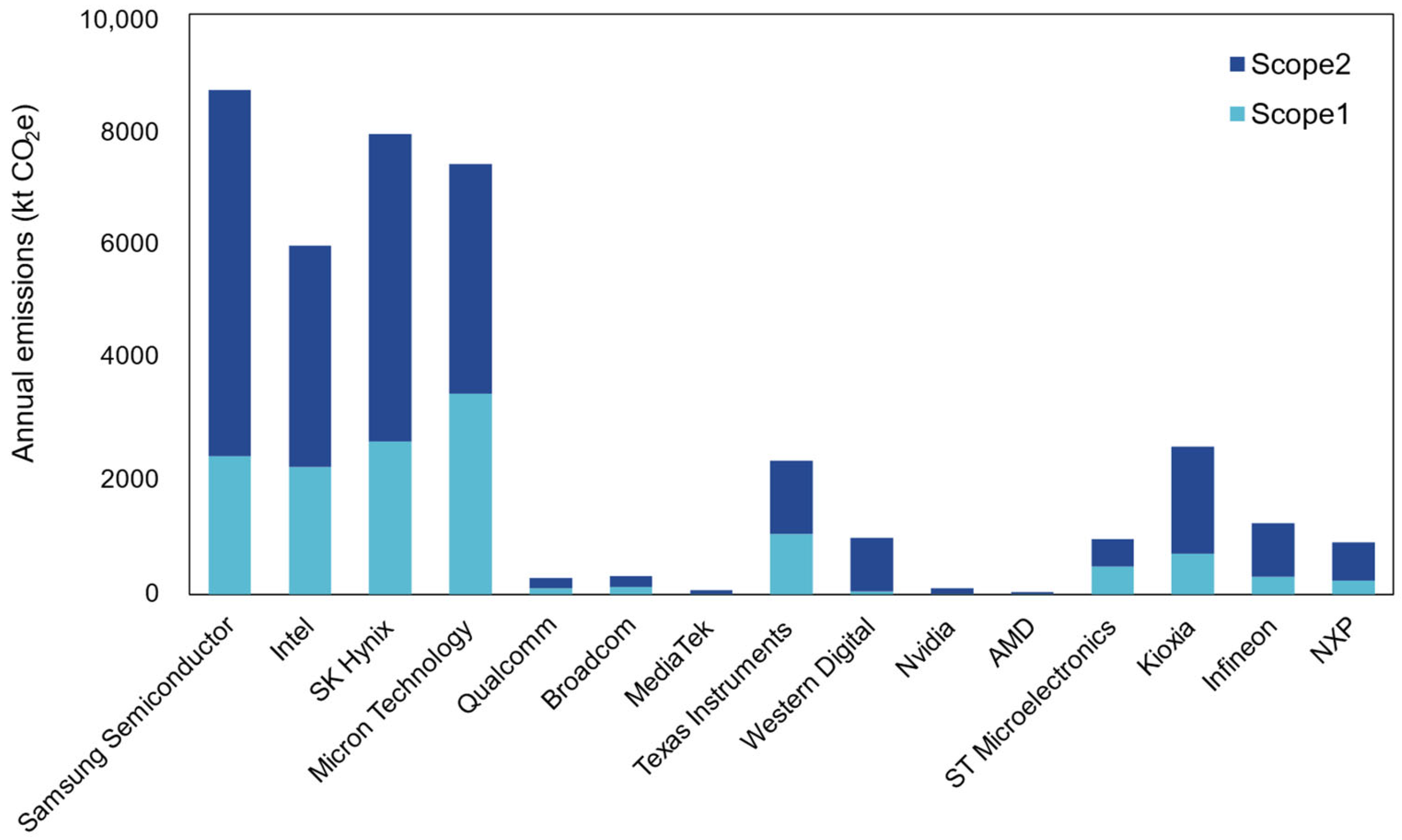

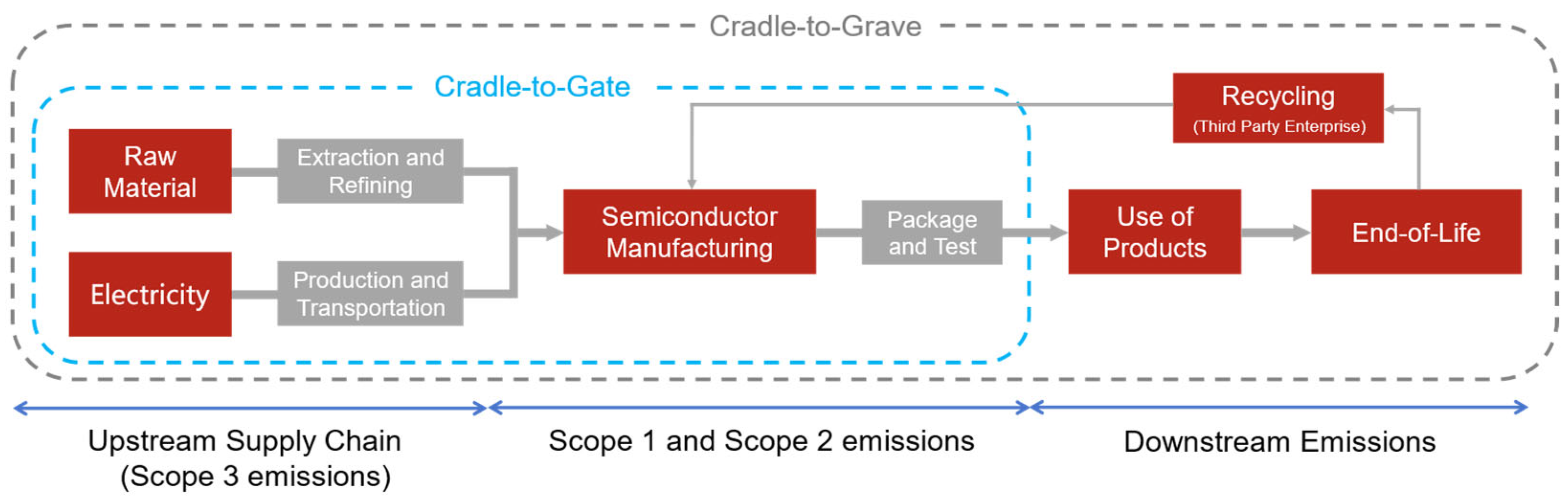
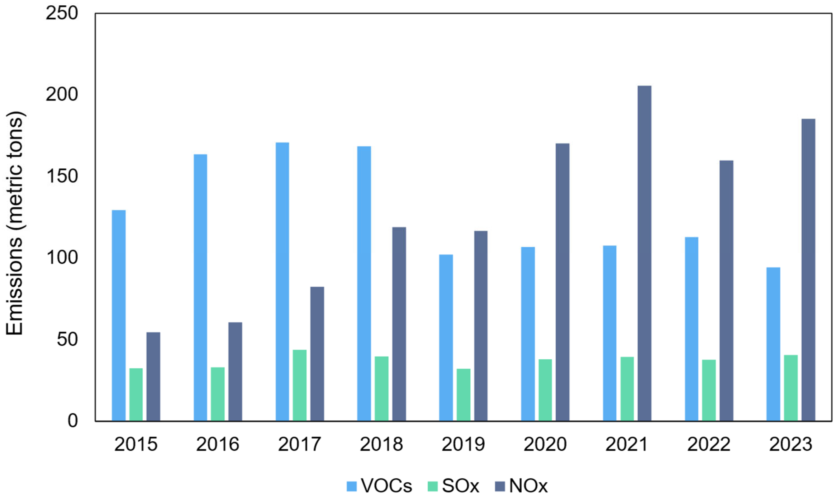


Disclaimer/Publisher’s Note: The statements, opinions and data contained in all publications are solely those of the individual author(s) and contributor(s) and not of MDPI and/or the editor(s). MDPI and/or the editor(s) disclaim responsibility for any injury to people or property resulting from any ideas, methods, instructions or products referred to in the content. |
© 2025 by the authors. Licensee MDPI, Basel, Switzerland. This article is an open access article distributed under the terms and conditions of the Creative Commons Attribution (CC BY) license (https://creativecommons.org/licenses/by/4.0/).