Abstract
A high-precision time reference is fundamental to the positioning, navigation, and timing (PNT) of global navigation satellite systems (GNSS). The precision of clock steering determines the accuracy of practical applications that rely on the time–frequency reference. With the invention of direct digital synthesizer (DDS) technology, digital clock steering (DCS) has gradually become a mainstream technology. However, the key factor limiting DCS accuracy is the system quantization noise, which leads to a low frequency and phase adjustment accuracy. Here we propose a DCS method based on - modulation to address the issue of low resolution of DAC through shaping the quantization noise. A simulated GNSS time–frequency reference system experimental platform is constructed to validate the effectiveness of the proposed method. The experimental results demonstrate that this method achieves a phase adjustment accuracy of 0.48 ps and a frequency adjustment accuracy better than 0.48 pHz, which is two orders of magnitude higher than that of existing GNSS time–frequency reference systems. Thus, the proposed method offers a significant improvement in time–frequency reference systems, leading to better performance, reliability, and accuracy in a wide range of practical applications.
1. Introduction
High-precision positioning, navigation, and timing (PNT) services are provided by global navigation satellite systems (GNSS), which rely on a high-precision time–frequency reference [1,2]. The time–frequency reference sources of major navigation satellites commonly comprise multiple long-term stable onboard atomic clocks and short-term stable high-quality crystal oscillators. The generation of the atomic timescale (ATS) and clock steering are the two main components of a time–frequency reference system. The global positioning system (GPS) time–frequency reference is produced by a timekeeping system (TKS). A TKS operates by comparing the phase difference between the reference atomic clock and the output of a highly stable crystal oscillator, it then adjusts the frequency by using a loop filtering algorithm. Next, the signal is converted to a voltage-controlled voltage by a digital-to-analog converter (DAC) to ensure that the output time–frequency signal is locked to the reference frequency source. The phase measurement accuracy of the TKS is 0.8 ps, whereas the frequency adjustment accuracy is 1 µHz [3]. The Galileo satellite, which is based on GPS TKS technology, employs a clock monitoring and control unit (CMCU) with a phase measurement accuracy of 24 ps and a frequency adjustment accuracy of 0.056 µHz as its onboard time–frequency reference equipment [4]. The time–frequency reference equipment for the Beidou-3 satellite is designed considering the advantages of a TKS and CMCU. Thus, the satellite achieves a phase measurement accuracy of 0.4 ps, frequency adjustment accuracy better than 30 nHz, and phase adjustment accuracy better than 0.1 ns [5]. Currently, the phase measurement accuracy of mainstream GNSS time–frequency reference equipment has reached the subpicosecond level. However, the phase adjustment accuracy of clock steering is only 0.1 ns, constituting a difference of two orders of magnitude.
To further enhance the PNT service capabilities of navigation satellites, GPS-Block-IIIA, Galileo-CMCU+, and other mainstream GNSS have implemented several improvements to their time–frequency reference systems. For instance, the performance and robustness of clock exception handling can be improved by improving the exception handling algorithm [6], and the phase-hopping problem of traditional primary and standby clocks can be solved by using the working mode of composite atomic clocks [7]. To meet the requirements of the new-generation Beidou navigation satellite time–frequency reference system, Yi et al. [8] conducted research on the ATS production algorithm and clock steering technology and provided solutions to improve frequency stability and enable reliable applications of single-star autonomous timekeeping. However, current improvements in the time–frequency reference system primarily focus on enhancing reliability and robustness; there is a lack of research on improving steering accuracy. Nevertheless, improving the steering accuracy of the time–frequency reference is crucial not only for providing higher precision PNT services but also for solving fundamental scientific research problems, such as local Lorentz invariance [9] and gravitational redshift verification [10]. Therefore, this study focuses on a high-precision digital clock steering (DCS) method.
The role of clock steering is to convert the local paper time into physical time–frequency reference signals to achieve fine adjustments in frequency and phase. Traditional clock steering is performed using analog circuits, which suffer from long adjustment time, large size, and poor programmability. With the rapid development of digital integrated circuits, direct digital synthesizer (DDS) technology has emerged [11]. Although DDS can achieve frequency and phase adjustment, its output time–frequency signal often exhibits discontinuities that fail to meet the requirements of a high-precision time–frequency reference system. Currently, DCS technology typically comprises a combination of a digital phase-locked loop (DPLL) and DDS. Most studies on DCS technology have focused on reducing the noise of the DPLL and DDS. For instance, Chimakurthy et al. [12] proposed a nonlinear addressing scheme that adaptively varies the number of interpolation points to reduce the size of the read-only memory (ROM) and optimize the quantization noise of the DDS. Stevanovic et al. [13] derived an enhanced model for a GPS PLL using the reference deviation of the tracking error as the phase-jitter index to optimize the effect of PLL noise. In addition, Zhao et al. [14] introduced a sinusoidal encoder phase discrimination method based on the Kalman filter to enhance the noise suppression capability of digital phase-locked loop phase discrimination and eliminate phase errors related to acceleration. Cardenas Olaya et al. [15] provided a phase noise function based on the power and frequency of an external reference voltage source to aid in the prediction of the stability of a PLL with respect to the frequency and power of the external reference. Furthermore, Murphy et al. [16] used multiple phase discriminators (PDs) and a linear DAC for overclocking counting to eliminate quantization noise in the PLL. Dartizio et al. [17] proposed a bang-bang fractional-N PLL with quantization noise shaping to overcome the noise limitations of the PD. The analysis of the DPLL primarily focuses on reducing the noise from the PD and loop filter (LPF). However, the low resolution of the DAC results in high quantization noise, which is the primary reason for the lack of high accuracy in frequency and phase adjustments by DCS.
Using a DPLL alone in DCS is impractical, as it would require significant time to manually adjust the phase by changing the frequency. Similarly, traditional phase shifters cannot be used independently [18], owing to issues such as sudden phase hopping and discontinuous phase tracking. To address these challenges, this study proposes a DCS method based on discrete - modulation. This study aims to resolve the quantization noise resulting from the low resolution of the DAC while enabling high-precision and continuous frequency and phase adjustments. We offer important insights into the enhancement of the steering accuracy of time–frequency reference signals, which is of significant research value for high-performance time–frequency reference systems in the next generation of GNSS.
2. Methodology
In this section, we present the transfer function of the DCS noise model and analyze the noise in each component of the model. The results of the analysis revealed that the most significant factor affecting the phase adjustment accuracy was the quantization noise resulting from the low resolution of the DAC. To address this issue, we proposed a DCS method based on discrete - modulation. Furthermore, a method based on augmented Lagrangian optimization was designed to ensure the best performance of the - modulator. Finally, we designed a loop filter to ensure clock steering speed while maintaining steer accuracy.
2.1. Noise Analysis
Noise analysis is a crucial step for understanding the precision of DCS. The noise model of DCS can be treated as a linear system, with each component introducing independent and uncorrelated random noise. The total phase noise was calculated, and the power spectral density of the output phase noise was analyzed. Figure 1 illustrates the noise transfer model of the DCS model, comprising the DDS, PD, LPF, DAC, and voltage-controlled oscillator (VCO), each of which contributes to the introduced noise.
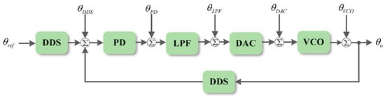
Figure 1.
Digital clock steering noise transfer function model.
The noise transfer function of the output signal is expressed as follows:
where z is a complex variable, is the PD gain, is the LPF gain, N is the allocation coefficient of the frequency divider, is the transfer function of the LPF, and is the transfer function of the VCO.
The phase noise power spectrum of the output signal can be generated by employing the superposition theorem. The obtained phase noise power spectral density of the output signal is expressed as follows:
where f is the frequency.
Based on noise theory analysis, the main sources of noise are the DDS, DAC, frequency source, and PD. The level of noise introduced by a DDS depends on its frequency control word (FCW) and phase control word (PCW). The quantization noise can be reduced by increasing the number of bits in the FCW and PCW. Similarly, it can be minimized in a purely digital PD by increasing the number of bits. Thus, the quantization noise can be characterized as independent and uniformly distributed white noise, with the quantizer power spectral density given by
where is the sampling rate and is the quantization noise range.
Frequency source noise is inevitable and is often represented as a linear combination of five independent noises [19]. To mitigate this noise, selecting a clock with a higher accuracy can be beneficial. The power spectral density of the frequency source noise is given by
where f is the Fourier frequency, is the amplitude, and is the power-law spectral index.
The quantization noise introduced by the DAC can be mitigated by increasing its resolution. However, it is currently challenging to fulfill the requirements of a time–frequency reference system. Moreover, a higher-resolution DAC is often associated with a higher cost. Consequently, upgrading the hardware to address the issue of a low-resolution DAC and the resulting quantization noise may not be the most effective solution.
2.2. Discrete - Modulator Design
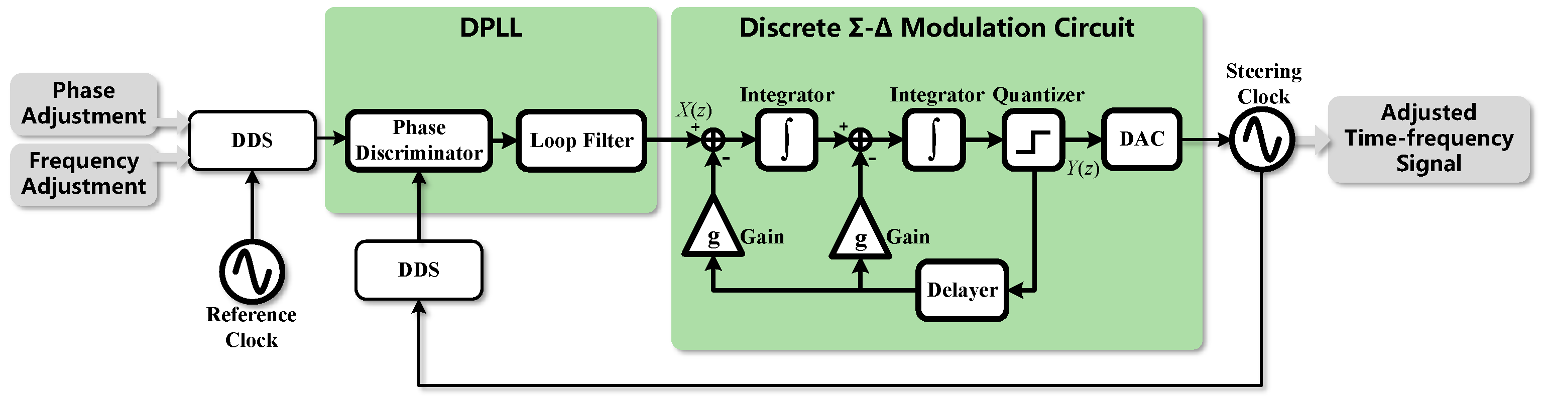
We designed a discrete - modulator to shape the quantization noise caused by insufficient resolution of the DAC. Figure 2 depicts the DCS model based on discrete - modulation. In this model, the reference and steering clocks function as sampling clocks for the two DDSs. Frequency and phase adjustments of the DDSs were achieved by varying the FCW and PCW. The phase discrimination of the output time–frequency signals from the two DDSs were carried out by the DPLL. The resulting phase difference is converted into digital frequency adjustment signals via loop filtering; it is then converted into an analog voltage-controlled voltage by the discrete - modulator. Ultimately, this voltage regulates the steering clock, thereby enabling the accurate output of the time–frequency signal after frequency and phase adjustments. The system transfer function of the DCS based on discrete - modulation can be represented as follows:
where is the transfer function of the DCS system and is the transfer function of the discrete - modulator.
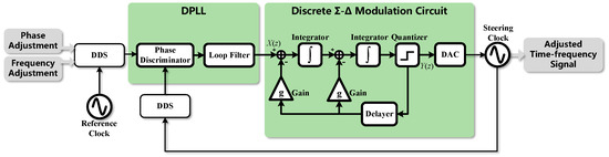
Figure 2.
DCS model based on discrete - modulation.
In the DCS model, the phase adjustment is accomplished by integrating the frequency adjustment. After the phase difference signal passes through a high-order loop filter, the output includes not only the filtered result of the phase difference but also high-order information such as the speed and acceleration of phase difference changes [20]. In a discrete - modulator, the input is a frequency-adjusted signal, which is the integral of the phase signal. Therefore, can be represented as:
where is frequency step amplitude, is frequency increment magnitude, and is unit step sequence. Its z-transform is:
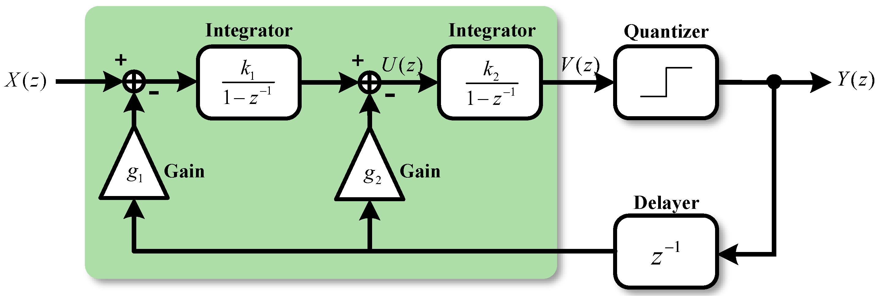
According to the final value theorem, we need to design a second-order - modulator to ensure that the steady-state error of the system is 0. Figure 3 shows the transfer function model of a second-order discrete - modulator.
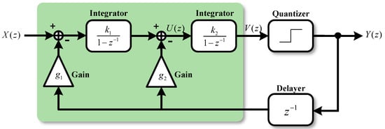
Figure 3.
Transfer function model of a second-order discrete - modulator.
Based on the system block diagram of the second-order discrete - modulator, the noise transfer function can be defined as follows:
where is the noise transfer function of the discrete - modulator, and are the gain of the integrator, and are the loop gain, and is the noise transfer function introduced by the quantizer, which can be seen as a type of uniformly distributed noise. The noise transfer function of can be defined as follows:
where is the resolution of the DAC.
To achieve system convergence, with all zeros and poles of the system transfer function inside the unit circle, we provide constrains as follows:
where , , , and are functions for finding zeros and poles.
The frequency adjustment resolution is primarily influenced by the DAC reference voltage and DAC resolution. Equation (11) represents the calculation formula for the frequency-adjustment resolution.
where is the frequency-adjustment resolution, is the DAC reference voltage, and N is the DAC bit.
The minimum resolution of the voltage-controlled voltage output of the DAC is directly proportional to the frequency-adjustment resolution, which differs from the frequency adjustment accuracy. The frequency adjustment resolution refers to the minimum resolution of the actual tuning frequency of the VCO output, which is determined by the hardware parameters.
To enhance the accuracy of frequency and phase adjustments, it is important to analyze the relationship between the DCS frequency and phase and the loop update period, while also designing the gains for the - modulator. Additionally, increasing the value of g provides a loop with sufficient gain, improves the tracking capabilities, and reduces the steady-state error in the DCS model. Moreover, decreasing the value of k helps to control the range of .
The objective function can be represented as follows:
where is the frequency adjustment deviation between the actual value and the ideal value, with minimax values reducing quantization errors.
Combining Equations (10) and (12), the - modulator design problem can be posed as follows:
Equation (13) represents a minimax optimization problem with constraints. We solve it using the augmented Lagrangian method [21]. The augmented Lagrangian function is as follows:
where is the penalty parameter, , , , and are Lagrangian multipliers, and , , , and are slack variables.
The algorithm is implemented as follows:
- (1)
- Update , , , and , by solving Equation (14), we find the optimal value of , , , and .Variables , , , and appear only in the two terms of Equation (14), which is actually a convex quadratic function of each relaxation variable. We take the partial derivative of . The unconstrained minimum of Equation (14) with respect to occurs when the partial derivative equals 0. If this is an unconstrained minimum, which has a lower bound less than 0, then it is convex in Equation (14). The optimal solution for in Equation (13) is 0. Therefore, the solution to Equation (13) is:
- (2)
- Update , , , and by:
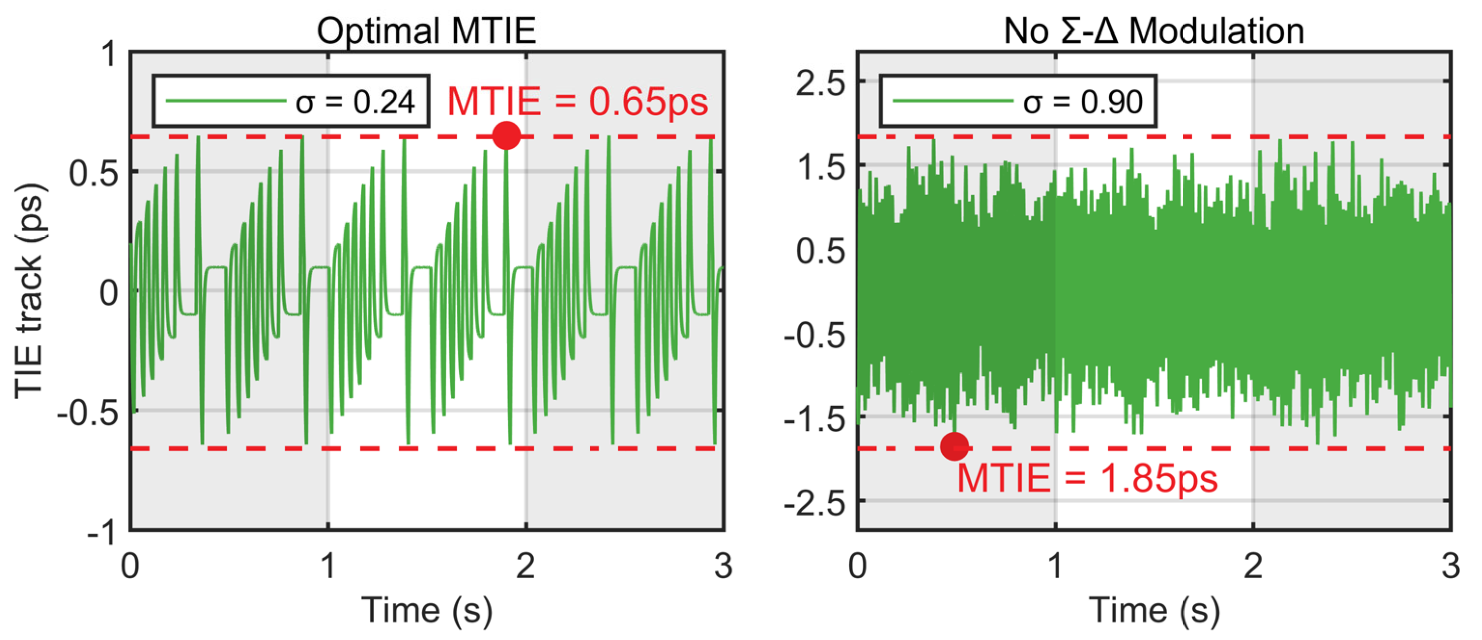
Then, continuously repeat steps 1 and 2. Upon meeting the termination conditions, the optimal - modulation gain is obtained. Figure 4 shows the TIE trace of the optimal MTIE and without the use of - modulation.
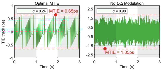
Figure 4.
TIE trace of optimal MTIE and without the use of - modulation. The green line represents TIE. The left part of the figure illustrates the optimal MTIE situation, and the right part shows TIE tracking of the no - modulation situation.
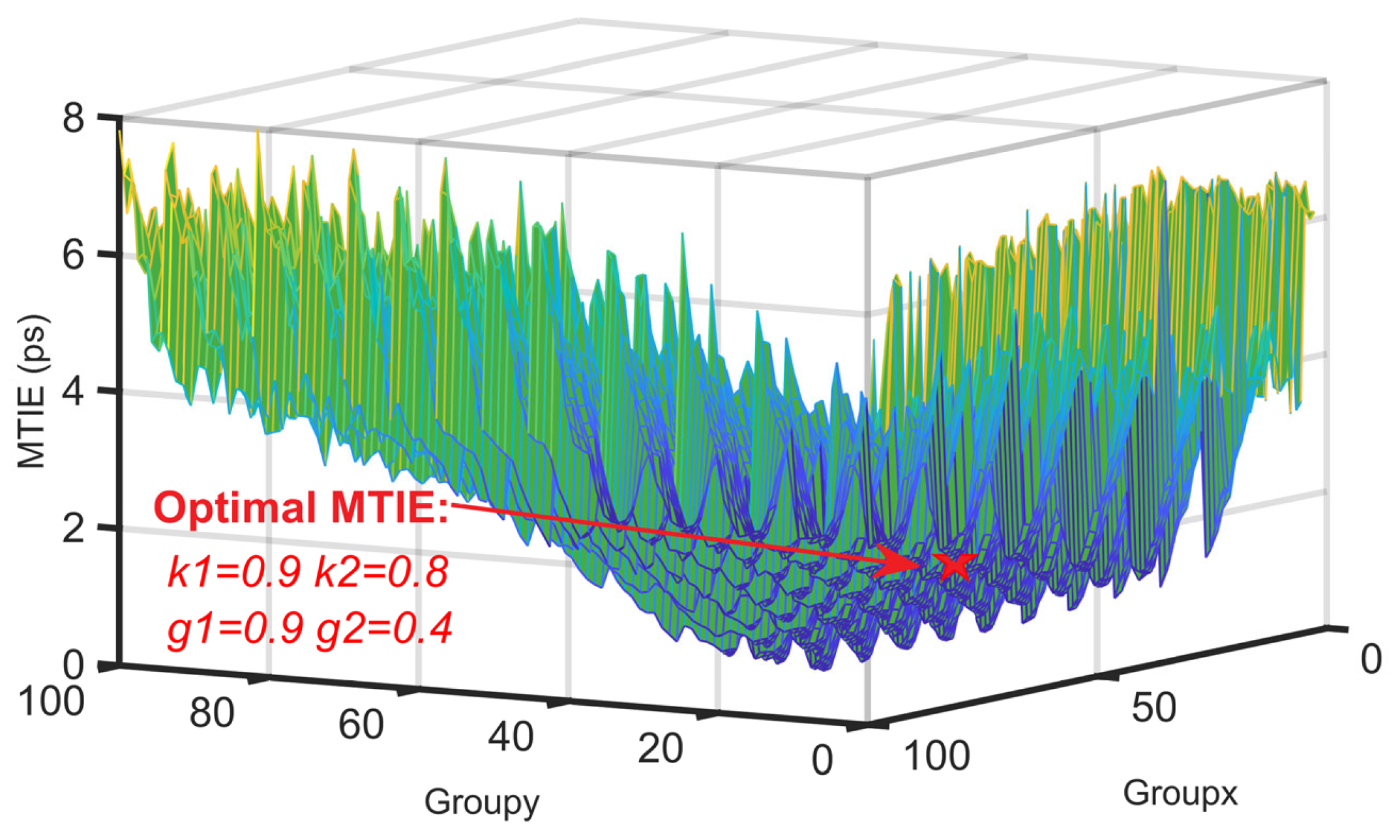
To validate the correctness of the optimization algorithm results, we conducted Monte Carlo simulations using the values of k1, k2, g1, and g2. During the simulations, we used a performance metric: the maximum time interval error (MTIE). The goal was to determine the optimal parameter values corresponding to this metric. Figure 5 shows the Monte Carlo simulations for finding the optimal MTIE result. The optimal MTIE result of the Monte Carlo simulations is consistent with the derived results of the augmented Lagrangian method. Simulation conditions are as follows.

Figure 5.
Monte Carlo simulations for finding the optimal MTIE result. We conducted Monte Carlo simulations using the values of k1, k2, g1, and g2. These parameters were varied within the range [0.4, 1.3] using a uniform distribution with 10 values for each variable. A total of 10,000 Monte Carlo simulations were performed. We used 100 different combinations of k1 and k2 as the x-axis, 100 different combinations of g1 and g2 as the y-axis, with MTIE as the z-axis.
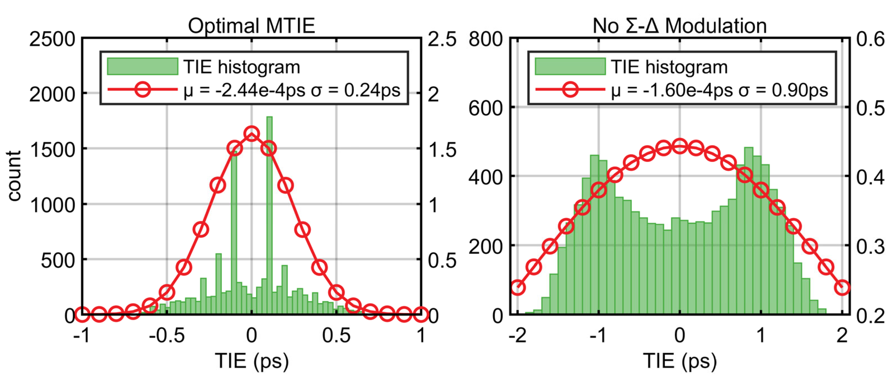
In Figure 6, we compare the TIE histograms with different - modulator gain values and without the use of - modulation. A TIE histogram provides a direct analysis of the various characteristics of the TIE. When the number of measurements, N, in the TIE was sufficiently large (N > 100), the TIE histogram effectively reflected its statistical characteristics. By comparing the TIE histograms, we can more directly observe and analyze the distribution and statistical properties of the TIE, which thereby enables us to evaluate the performance improvements achieved by the proposed method.
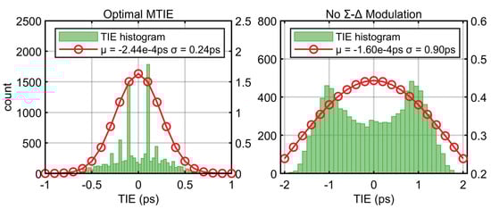
Figure 6.
TIE histogram of optimal MTIE and without the use of - modulation. The left part of the figure shows the TIE histogram under the optimal MTIE condition, and the right part shows the TIE histogram under the condition of not using the - modulator.
In this study, the TIE was transformed into a frequency-tracking error. Notably, the frequency-tracking error differs from the frequency-adjustment resolution. The frequency-adjustment resolution refers to the minimum resolution of the actual tuning frequency of the output from the VCO. In contrast, the frequency-tracking error is the result of the phase-value determination. According to Equation (17), under the optimal MTIE conditions, the frequency-tracking error was calculated to be 0.24 pHz.
where is the time interval used to calculate the frequency. The time–frequency signal is often used for counting to generate a one pulse per second (1PPS) signal. Here, we take as 1 s.
2.3. Optimal LPF Design
The performance of a - modulator is directly affected by the phase difference filtering results of the LPF, as it serves as the input to the - modulator. At the same time, the LPF design is crucial for determining the dynamic and steady-state characteristics of the PLL. We empirically designed the loop bandwidth and loop update period to achieve a PLL that meets the requirements of a steady-state error, locking time, overshoot, and other factors. Equation (18) provides a formula for the loop bandwidth of a third-order PLL:
where and are the classical parameters of the third-order LPF and is the characteristic frequency of the phase-locked loop.
The equivalent noise bandwidth of a DPLL can be approximated as a function of the closed-loop system frequency response .
Rewrite Equation (19) as follows:
where the integral of the circumference , its integral path, is a unit circle.
Derive the relationship between the loop bandwidth of a third-order DPLL and the loop bandwidth of an analog PLL by combining Equations (18), (20), and (21).
where , , and are the classical parameters of the third-order LPF; is the analog third-order PLL loop bandwidth; and is the loop update period.
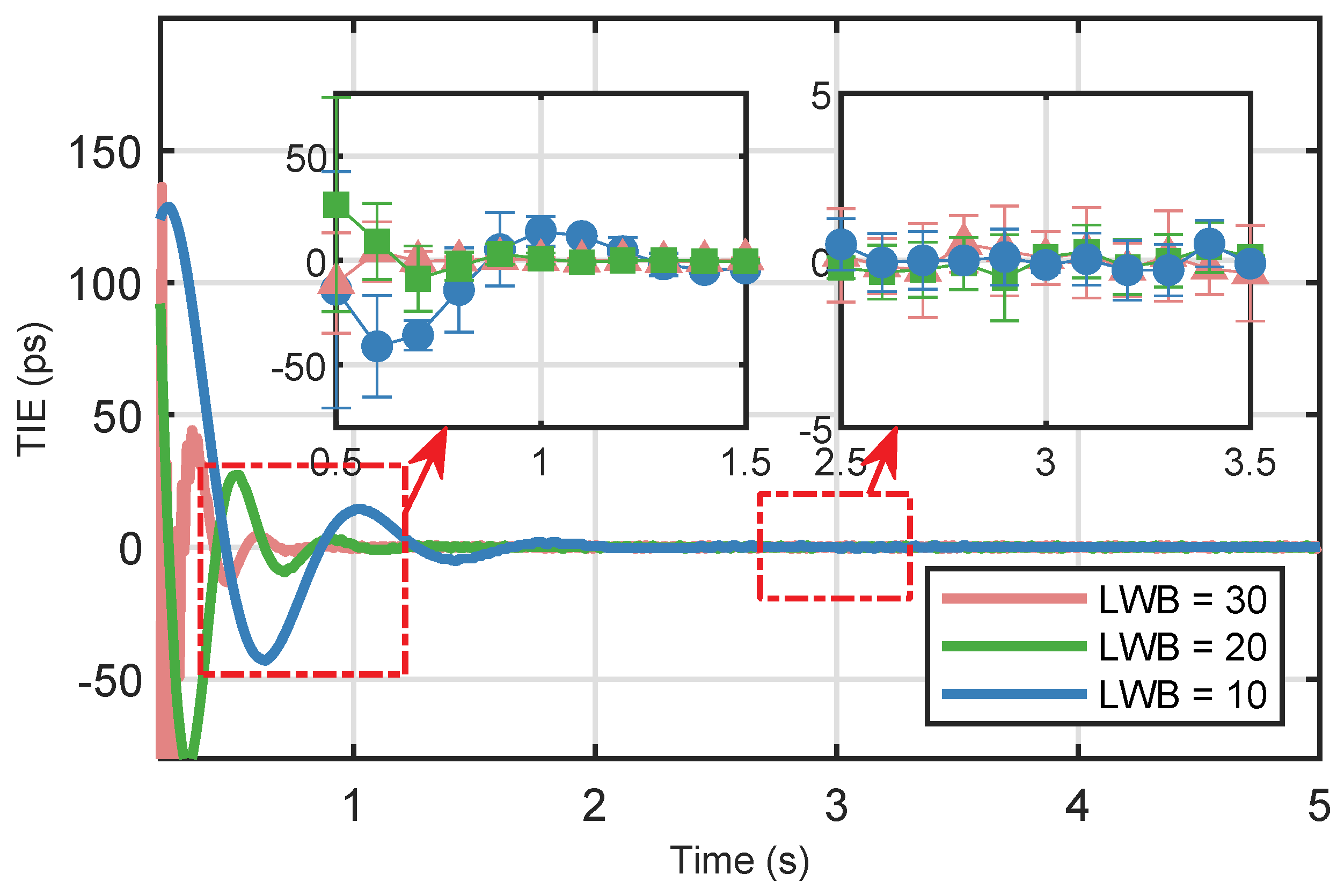
The simulation results of the optimal loop bandwidth in Figure 7 show that, when is 20, the locking time of the PLL is 1 s, when is 30, the locking time of the PLL is 1 s, and, when is 10, the lock time of the PLL is 1.5 s. The steady-state errors of the DPLL were equal for different loop bandwidths. Reducing the loop bandwidth of the DPLL increased the locking time; however, the phase-tracking accuracy did not improve after the PLL stabilized.
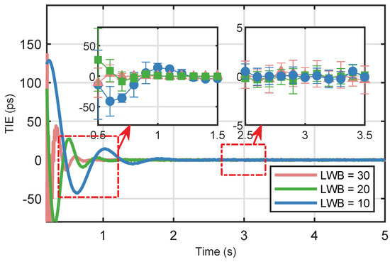
Figure 7.
Locking times and steady-state errors of DCS at different loop bandwidths. The red line represents the lock time under a loop bandwidth of 30, the green line represents the lock time under a loop bandwidth of 20, and the blue line represents the lock time under a loop bandwidth of 10.
Therefore, the design concept behind the DPLL loop bandwidth and loop update period aims to maximize the loop tracking accuracy by appropriately increasing the loop bandwidth and accelerating the loop update period. This approach achieves a high level of precision and fast loop locking.
3. Simulation
In this section, we use simulation software to conduct DCS simulation verification based on the system block diagram and the designed - modulator and the optimal loop bandwidth. Our aim is to achieve a high-precision and rapid response. Algorithm 1 shows the pseudocode of system simulation. Table 1 lists the parameters used in the simulations. These simulation parameters were selected based on the actual hardware parameters to ensure the accuracy and reliability of the verification results.
| Algorithm 1: System simulation |
|

Table 1.
Simulation parameter setting.
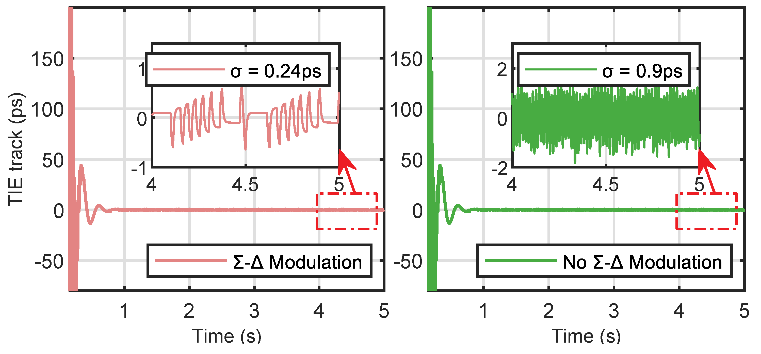
The simulation results indicate that the loop-lock time achieved is 1 s. When the method proposed in this study was not used, the phase-tracking error was measured to be 0.9 ps, and the frequency-tracking error was 0.9 pHz. However, by designing the optimal loop bandwidth and - modulator gain as suggested, significant improvements are observed. The phase tracking error is reduced to 0.24 ps, and the frequency tracking error is reduced to 0.24 pHz. These findings highlight the effectiveness of the proposed method in achieving superior performance in terms of reducing the tracking errors. It is important to note that k1, k2, g1, and g2 are not constant values. They need to be determined based on different systems using the methods provided in this paper (Figure 8).
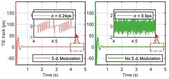
Figure 8.
Simulation results of the adjustment time and adjustment accuracy. The red line represents the overall simulation under the optimal design of the - debugger, while the green line represents the overall simulation without using the - modulator.
In practice, phase adjustment in DCS can be achieved by compensating for the phase-difference signal from the PD. The accuracy of this adjustment process is determined by the number of bits in the phase-difference signal and the tracking error. In a DPLL, the number of bits in the phase-difference signal is typically high, and inherent errors can be considered negligible. Therefore, the phase and frequency adjustment accuracies were primarily limited by the tracking errors with higher weights. With a phase tracking error of 0.24 ps, the phase adjustment accuracy reached the subpicosecond level, which is comparable to the precision of phase measurements in GNSS time–frequency reference systems. Similarly, the frequency adjustment accuracy was equal to a frequency-tracking error of 0.24 pHz. Through simulation results, the correctness of the theoretical derivations and the effectiveness of the DCS method based on discrete - modulation have been effectively demonstrated.
4. Experiments
To assess the effectiveness of the DCS method based on discrete - modulation in a practical setting, we established a simulated GNSS time–frequency reference system experimental platform following the system block diagram and theoretical analysis. This section presents the design of the experimental process, including the details of the hardware parameters and instrument settings. The errors were analyzed and treated; this was followed by the execution of the experiment. The resulting experimental data are presented, analyzed, and discussed to enable the evaluation of the obtained results.
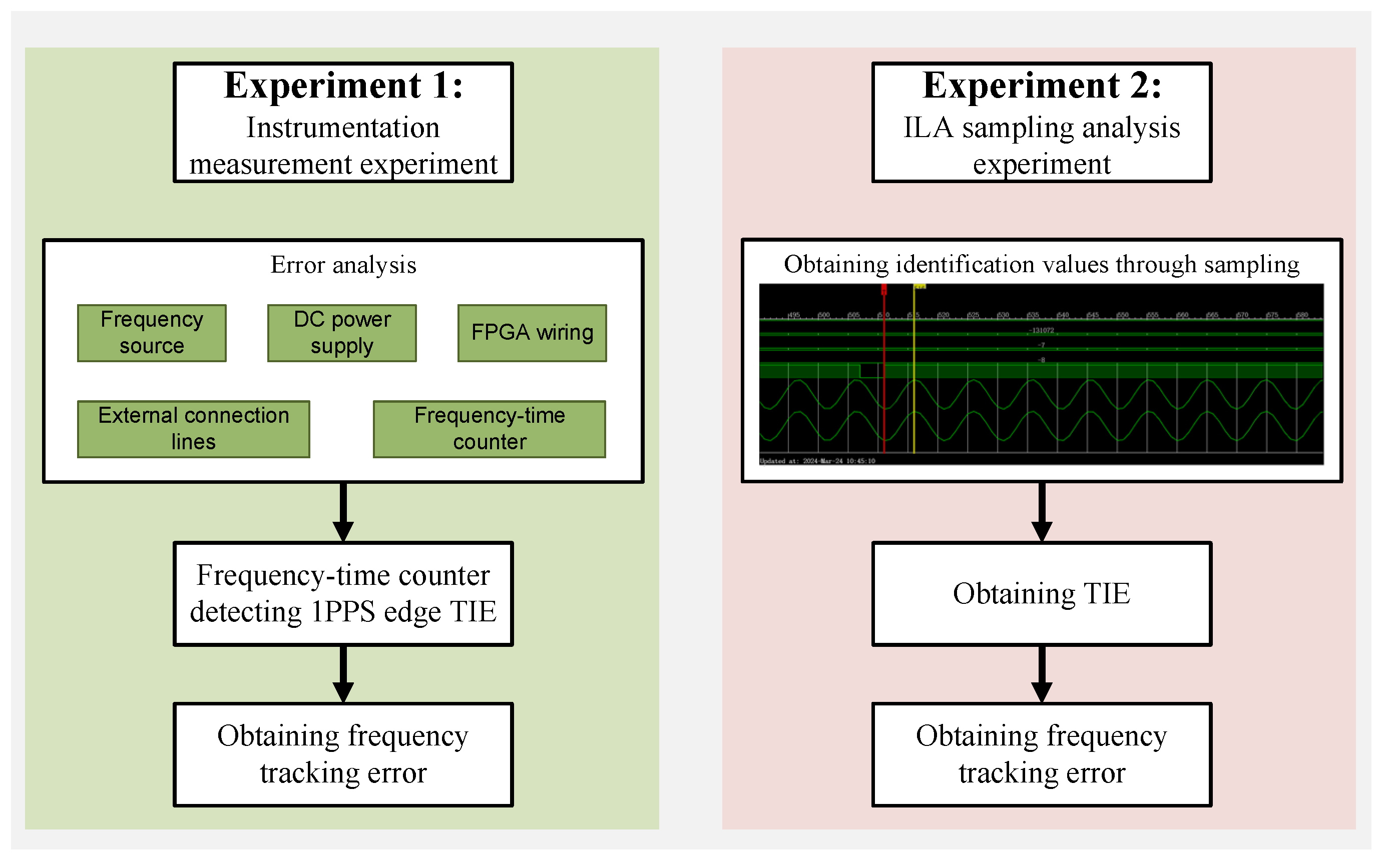
Two experiments were conducted to evaluate the effectiveness of the proposed method from different perspectives. The experimental flow diagram depicted in Figure 9 shows the design of the two physical experiments: an instrument measurement experiment and an ILA sampling analysis experiment. The integrated logic analyzer (ILA) is an IP core provided by the Vivado software package. It enables the in-system debugging of the FPGA device and enables the real-time capture of waveform data from digital signals within the FPGA using one or more probes. The ILA serves as a valuable tool for performing detailed analysis of the captured data.
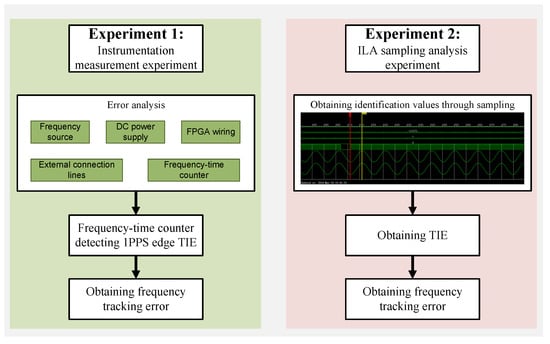
Figure 9.
Experimental process.
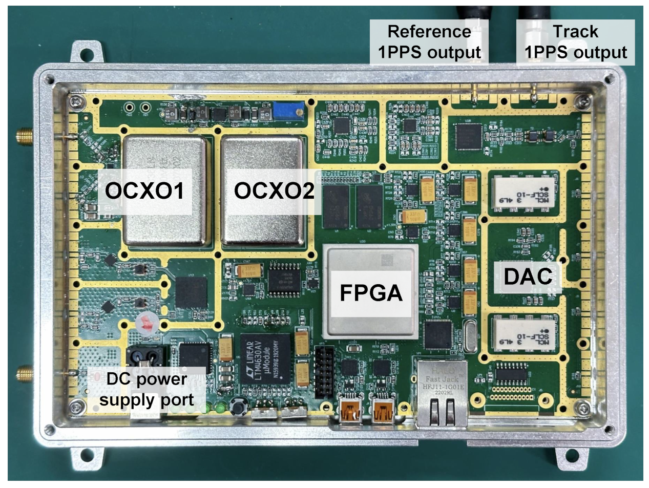
Figure 10 illustrates the design of an integrated time–frequency reference unit based on an FPGA. It consists of two oven-controlled crystal oscillators (OCXOs), an FPGA, a DAC, and various input–output interfaces. OCXO1 simulates ATS production, whereas OCXO2 serves as a highly stable crystal oscillator for precise clock steering. Figure 11 shows the experimental platform of the constructed simulated GNSS time–frequency reference system.

Figure 10.
Integrated time–frequency reference unit.
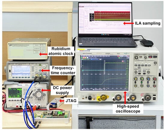
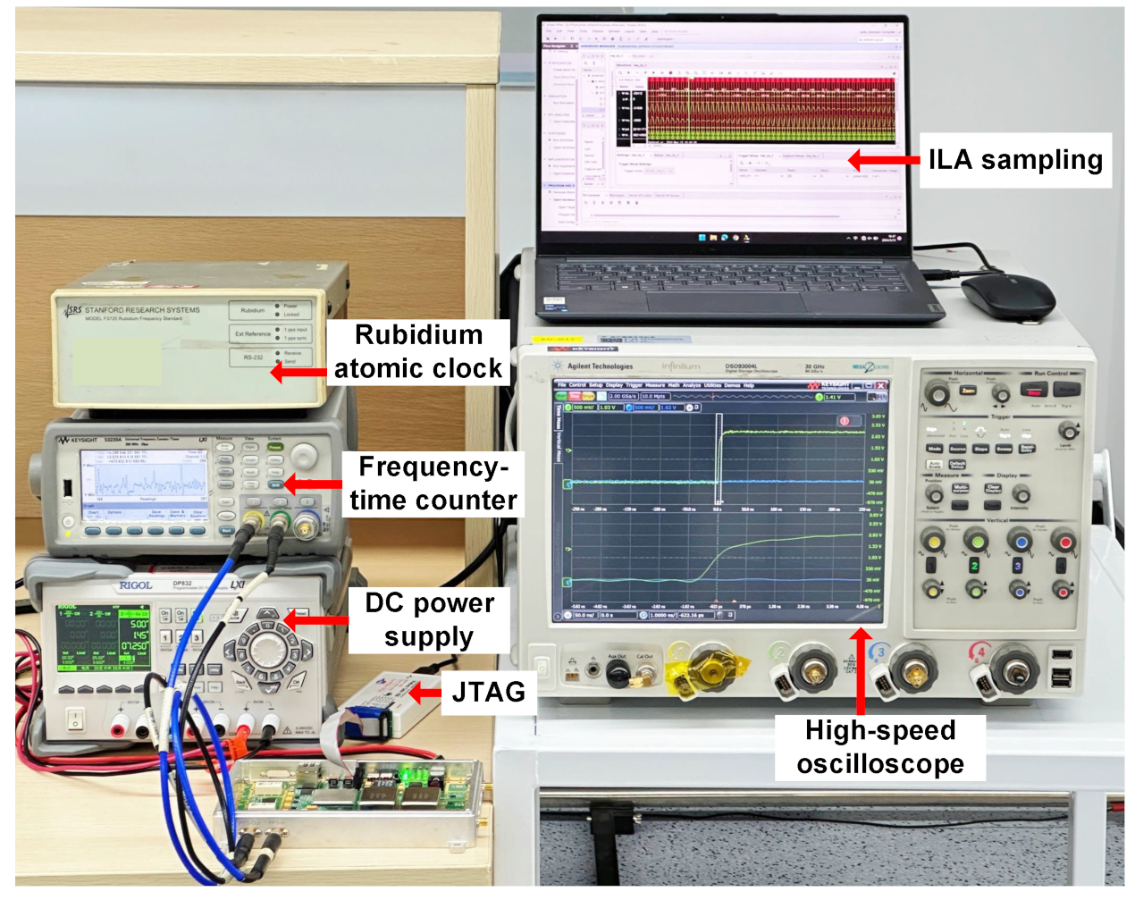
Figure 11.
Simulated GNSS time–frequency reference system experimental platform. Includes an integrated time–frequency reference unit, rubidium atomic clock, frequency-0time counter, DC power supply, JTAG, high-speed oscilloscope, and integrated logic analyzer.
4.1. Instrumental Measurement Experiment
Compared with the simulation experiment, the experimental platform of the time–frequency reference system introduces additional sources of errors that exhibit higher levels. These factors are challenging to precisely model and analyze in a simulated environment. First, we thoroughly examined the experimental environment and identified the various sources of noise. Table 2 lists the sources of noise and characteristics. These include internal noise originating from the frequency source, noise associated with the DC power supply, noise introduced through the FPGA timing jitter, and the internal noise of the frequency–time counter. Notably, the short-term stability of the OCXO employed in the experiment was only 1 ×. Additionally, the OCXO is susceptible to variations in the temperature and power supply voltage. Table 3 lists the key electrical performance indicators of the OCXO. The power supply noise can affect the OCXO power supply voltage, resulting in frequency changes. Furthermore, it can affect the reference voltage of the DAC, thereby reducing the accuracy of the voltage control signal. Table 4 lists the parameters of the devices and instruments used in the experiments.
Table 2.
Sources of noise and characteristics.
Table 3.
Key electrical performance technical indicators of OCXO.
Table 4.
Main device and instrument parameters.
We carried out comprehensive testing of each instrument device used in the experimental setup. First, we assessed the capabilities of the DAC by outputting the maximum and minimum voltages. We then monitored the corresponding adjustable range of the OCXO frequency. The test results indicate that the OCXO frequency can be adjusted within a maximum range of [−10 Hz, 10 Hz], which consequently affects the resolution of the frequency adjustments. Subsequently, a high-speed oscilloscope was used to measure the edge steepness of the FPGA. This measurement is critical because it directly affects the accuracy of the time interval measurement between the 1PPS signals obtained by counting the output signal of the OCXO.
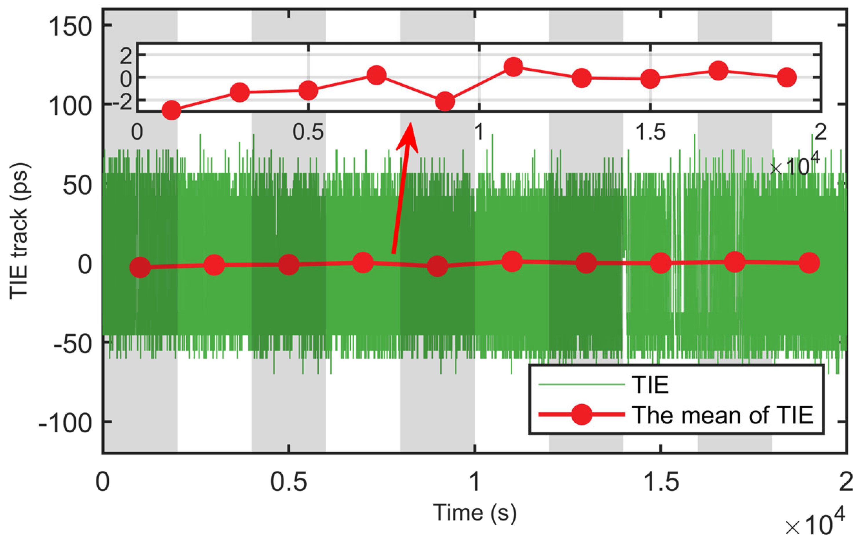
The accuracy of the frequency–time counter is of crucial importance because it determines the precision with which we can detect time intervals. We used two same-source 1PPS signals generated by a rubidium clock as inputs into the frequency–time counter. Theoretically, the time interval between these identical 1PPS signals should be 0. We utilized the rubidium clock count to generate two same-source 1PPS signals. These signals were then input into the frequency–time counter for measurement while continuously sampling for a duration of 20,000 s at a rate of 1 Hz. Figure 12 show that the peak-to-peak width of the TIE for the two same-source 1PPS signals is 120 ps, which falls short of meeting the requirements of our detection simulation results. To address this, we calculated the mean of the TIE every 2000 s. The mean peak-to-peak width of TIE is 5 ps, which originates from measuring errors of the instrument.
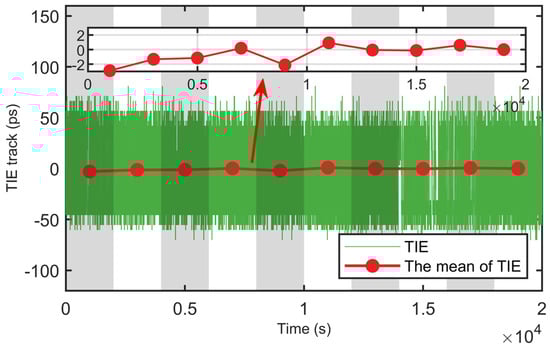
Figure 12.
TIE track of same-source 1PPS signals from a rubidium clock. The green line represents the actual sampled TIE, while the red line represents the mean TIE.
Similar to a rubidium atomic clock, we utilized the reference OCXO count from the integrated time–frequency reference generation unit to generate two same-source 1PPS signals. The peak-to-peak width of the TIE for the two same-source 1PPS signals is 120 ps, and the mean peak-to-peak width of the TIE is 5 ps.
Based on the results of the error analysis, the verification scheme for the proposed method was designed as follows. In this experiment, we introduced a reference OCXO and steering OCXO. After precise adjustments to their phase and frequency, these two OCXOs independently output 1PPS signals that were then transported into a locked state. The maximum mean TIE was detected by comparing the edges of these signals.
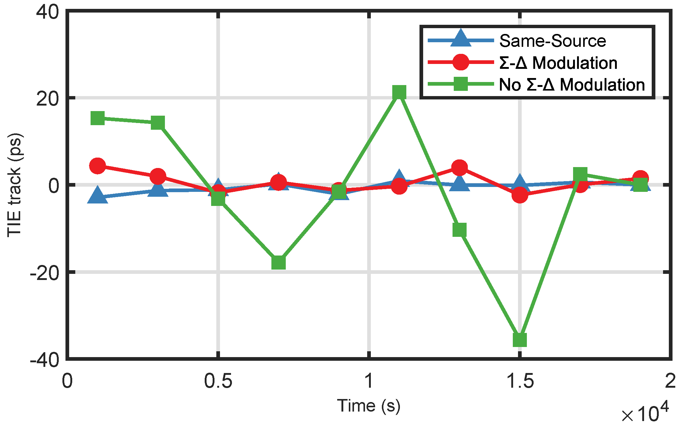
To evaluate the clock steering performance of the proposed method, we employed a 53230A frequency–time counter to measure the time interval between the edges of two non-same-source 1PPS signals. The TIE was then calculated as the mean over 2000 s. By comparing this TIE with the corresponding value obtained from the same-source 1PPS signals, we can verify whether the TIE reaches a similar level. The experimental results shown in Figure 13 and summarized in Table 5 highlight the performance of the proposed method and provide a quantitative evaluation of its effectiveness in achieving precise clock steering.
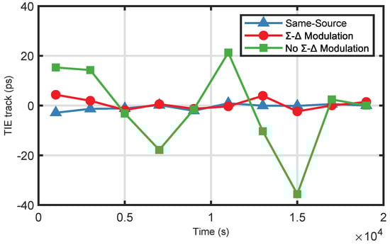
Figure 13.
Comparison of the measurement of the TIE track in the same-source, - modulation, and no - modulation cases. The red line represents the situation using a second-order - modulator, the green line represents the situation without using the - modulator, and the blue line represents the situation for same-source. It is important to note that these TIE tracks are non-periodic.
Table 5.
Comparison of the measurement of the TIE track in the same-source, - modulation, and no - modulation cases.
Equation (17) can be used to convert the TIE deviation into a frequency-tracking error. Notably, when we do not employ discrete - modulation, this results in a frequency tracking error of 40 pHz. However, if we were to utilize discrete - modulation, the frequency tracking error would be further reduced to less than 5 pHz. This highlights the advantages and improved precision of using discrete - modulation in our methodology.
The experimental results indicate that continuous sampling was conducted for 20,000 s at a sampling rate of 1 Hz. The phase adjustment accuracy is limited to 40 ps, and the frequency adjustment accuracy is 40 pHz when discrete - modulation is not used. However, when discrete - modulation is used, the phase adjustment accuracy is improved to a level comparable with that of the same-source TIE and achieves an accuracy better than 5 ps. In addition, the frequency adjustment accuracy is enhanced, reaching a level better than 5 pHz.
4.2. ILA Sampling Analysis Experiment
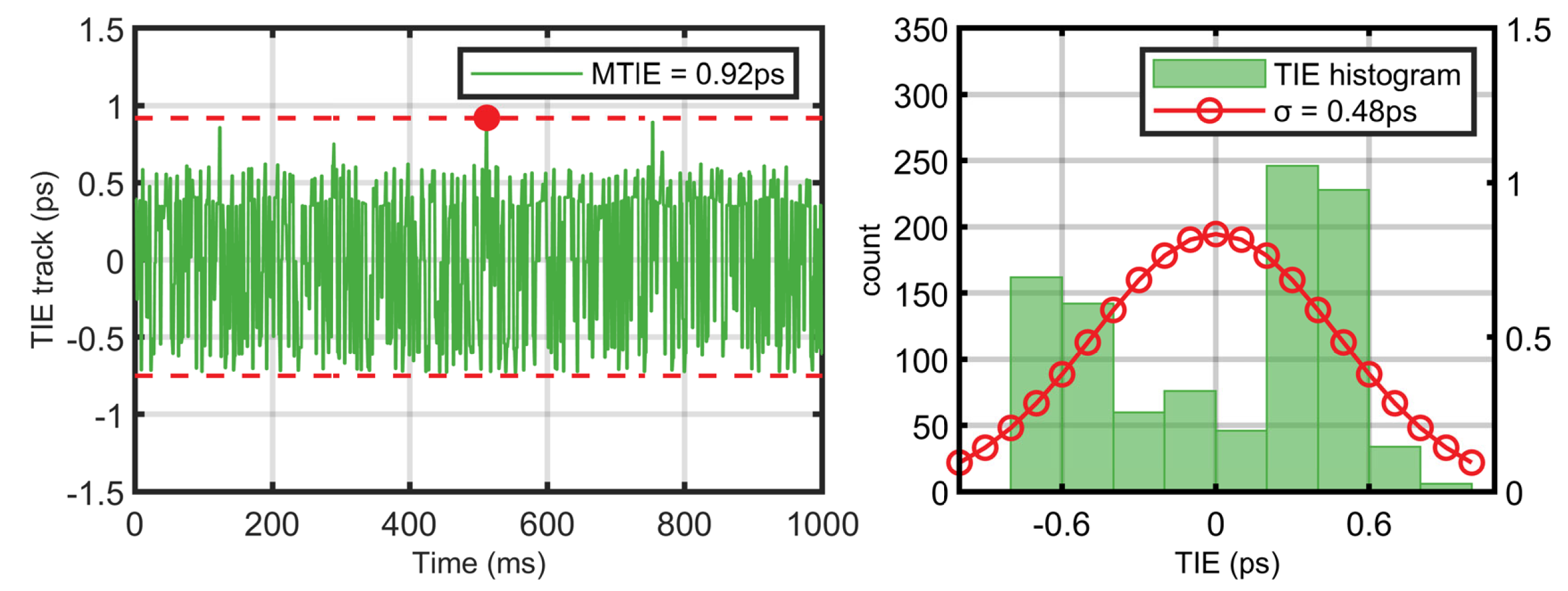
While we are unable to quantitatively measure the exact improvement in accuracy achieved by the DCS method based on discrete - modulation using the frequency–time counter, we can utilize the ILA debugging tool provided by the Vivado software package to capture the phase detection value. This value represents the phase difference between two 230 KHz sine wave signals generated by the DDS. Our designed phase detector uses a 32-bit signal. To collect the phase detection values, we continuously sample for a duration of 1000 ms; the OCXO output signal duration for one cycle is s. By analyzing and plotting these phase detection values, we can create a phase-tracking error diagram that captures the performance of our system.
Figure 14 clearly illustrates that the phase adjustment accuracy of the DCS method, based on discrete - modulation, is 0.48 ps. These results effective demonstrate that the phase adjustment accuracy of DCS reaches the subpicosecond level. Furthermore, by applying Equation (17) to calculate the frequency adjustment accuracy, we show it is 0.48 pHz.
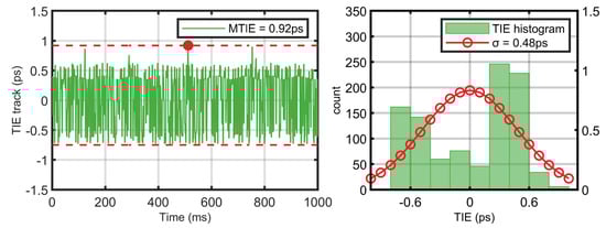
Figure 14.
ILA sampling second-order - modulation interval error. The red point of left part of the figure shows max TIE.
4.3. Discussion of Experimental Results
Considering the limitations imposed by the experimental environment and the noise present in the experimental instruments during Experiment 1, we can only conclude that the phase adjustment accuracy is better than 5 ps and the frequency adjustment accuracy is better than 5 pHz. In Experiment 2, where measurements were obtained via the use of the Vivado ILA debugging tool, the phase adjustment accuracy was determined to be 0.48 ps, with the frequency adjustment accuracy surpassing 0.48 pHz. The proposed approach offers a more effective solution to the challenge of quantization noise, thereby improving the overall accuracy of clock steering.
In fact, a functioning GNSS system, despite facing more complex thermal and electromagnetic noise compared with ground laboratories, is often designed with careful consideration. The internal electronic components are well protected, so the conclusions drawn by the laboratory are not significantly different from the actual situation. Moreover, our experimental design follows the actual payload ground verification standards. Finally, the performance of the atomic clock chosen for the GNSS time–frequency reference system is better than the frequency source selected in this paper. If the findings of this paper are applied to GNSS in the future, the accuracy of frequency and phase adjustments will be even higher.
5. Conclusions
In this study, we present a DCS method based on discrete - modulation to address the issue of quantization noise caused by the low resolution of the DAC. The DCS model is provided, and the error theory is analyzed. The main error component is the quantization noise stemming from the low resolution of the DAC. We present a discrete - modulation model and design the optimal - modulator using an augmented Lagrangian method, achieving high-precision clock steering. Furthermore, we provide a strategy for designing the optimal loop bandwidth accordingly. Simulation results demonstrate that, without using the - modulation circuit, the frequency and phase adjustment accuracy are 0.9 pHz and 0.9 ps, respectively. However, by using the method proposed in this study, the phase adjustment accuracy improves to 0.24 ps, and the frequency adjustment accuracy improves to 0.24 pHz. The experimental results confirm that this method yields a phase adjustment accuracy of 0.48 ps and a frequency adjustment accuracy better than 0.48 pHz. Remarkably, this represents an improvement of two orders of magnitude compared with the accuracy of existing GNSS time–frequency reference systems. The experimental findings strongly validate the effectiveness of the DCS method based on discrete - modulation, thereby confirming its capacity to enhance both frequency and phase adjustment accuracy.
The proposed method holds significant importance for enhancing the accuracy of GNSS time–frequency reference applications. Moreover, high-precision DCS offers a low-cost, lightweight, high-precision, and efficient means of achieving time–frequency synchronization in various fields, such as distributed communication, UAV collaboration, and basic scientific research.
Author Contributions
M.L. and Z.M. provided the initial idea and designed the experiments for this study; M.L. analyzed the data and wrote the manuscript; Z.M., E.Y. and S.L. helped with the writing. All authors reviewed the manuscript. All authors have read and agreed to the published version of the manuscript.
Funding
This research received no funding.
Data Availability Statement
The data presented in this study are available on request from the corresponding author. The data are not publicly available due to privacy.
Conflicts of Interest
The authors declare that the research was conducted in the absence of any commercial or financial relationships that could be construed as a potential conflicts of interest.
Abbreviations
The following abbreviations are used in this manuscript:
| GNSS | global navigation satellite systems |
| PNT | positioning, navigation, and timing |
| DCS | digital clock steering |
| DAC | digital-to-analog converter |
| DDS | direct digital synthesizer |
| DPLL | digital phase-locked loop |
| FPGA | Field Programmable Gate Array |
| ATS | atomic timescale |
| TKS | timekeeping system |
| CMCU | clock monitoring and control unit |
| PD | phase discriminator |
| LPF | loop filter |
| LUT | lookup table |
| VCO | voltage-controlled oscillator |
| FCW | frequency control word |
| PCW | phase control word |
| 1PPS | one pulse per second |
| MTIE | maximum time interval error |
| TIE | time interval error |
| ILA | integrated logic analyzer |
| OCXO | oven-controlled crystal oscillator |
References
- Tavella, P.; Petit, G. Precise time scales and navigation systems: Mutual benefits of timekeeping and positioning. Satell. Navig. 2020, 1, 10. [Google Scholar] [CrossRef]
- Guo, Y.; Li, Z.; Gong, H.; Peng, J.; Ou, G. Time–Frequency Signal Integrity Monitoring Algorithm Based on Temperature Compensation Frequency Bias Combination Model. Remote Sens. 2024, 16, 1453. [Google Scholar] [CrossRef]
- Petzinger, J.; Reith, R.; Dass, T. Enhancements to the GPS block IIR timekeeping system. In Proceedings of the 34th Annual Precise Time and Time Interval Systems and Applications Meeting, Reston, VA, USA, 3–5 December 2002; pp. 89–107. [Google Scholar]
- Felbach, D.; Heimbuerger, D.; Herre, P.; Rastetter, P. Galileo payload 10.23 MHz master clock generation with a Clock Monitoring and Control Unit (CMCU). In Proceedings of the IEEE International Frequency Control Sympposium and PDA Exhibition Jointly with the 17th European Frequency and Time Forum, Tampa, FL, USA, 4–8 May 2003; pp. 583–586. [Google Scholar] [CrossRef]
- Chen, Z.; Wu, X. General Design of the Third Generation BeiDou Navigation Satellite System. J. Nanjing Univ. Aeronaut. Astronaut. 2020, 52, 835–845. [Google Scholar] [CrossRef]
- Wang, Q.; Rochat, P. Algorithms Development and Verification for Next Generation On-board Clock Monitoring and Control Unit. In Proceedings of the 2019 Joint Conference of the IEEE International Frequency Control Symposium and European Frequency and Time Forum (EFTF/IFC), Orlando, FL, USA, 14–18 April 2019; pp. 1–5. [Google Scholar] [CrossRef]
- Wang, Q.; Rochat, P. ONCLE (One Clock Ensemble) for Galileo’s Next-Generation Robust Timing System. Navig. J. Inst. Navig. 2022, 69, navi.536. [Google Scholar] [CrossRef]
- Yi, X.; Yang, S.; Dong, R.; Ren, Q.; Shuai, T.; Li, G.; Gong, W. A composite clock for robust time–frequency signal generation system onboard a navigation satellite. GPS Solut. 2024, 28, 6. [Google Scholar] [CrossRef]
- Megidish, E.; Broz, J.; Greene, N.; Häffner, H. Improved Test of Local Lorentz Invariance from a Deterministic Preparation of Entangled States. Phys. Rev. Lett. 2019, 122, 123605. [Google Scholar] [CrossRef] [PubMed]
- Cacciapuoti, L.; Salomon, C. Space clocks and fundamental tests: The ACES experiment. Eur. Phys. J. Spec. Top. 2009, 172, 57–68. [Google Scholar] [CrossRef]
- Jenq, Y.-C. Direct digital synthesizer with jittered clock. IEEE Trans. Instrum. Meas. 1997, 46, 653–655. [Google Scholar] [CrossRef]
- Chimakurthy, L.; Ghosh, M.; Dai, F.; Jaeger, R. A novel DDS using nonlinear ROM addressing with improved compression ratio and quantization noise. IEEE Trans. Ultrason. Ferroelectr. Freq. Control 2006, 53, 274–283. [Google Scholar] [CrossRef]
- Stevanovic, S.; Pervan, B. A GPS Phase-Locked Loop Performance Metric Based on the Phase Discriminator Output. Sensors 2018, 18, 296. [Google Scholar] [CrossRef]
- Zhao, G.; Ban, Y.; Zhang, Z.; Shi, Y.; Liu, H. Phase Demodulation Strategy Based on Kalman Filter for Sinusoidal Encoders. IEEE Sens. J. 2023, 23, 10625–10632. [Google Scholar] [CrossRef]
- Cardenas Olaya, A.C.; Calosso, C.E.; Friedt, J.M.; Micalizio, S.; Rubiola, E. Phase Noise and Frequency Stability of the Red-Pitaya Internal PLL. IEEE Trans. Ultrason. Ferroelectr. Freq. Control 2019, 66, 412–416. [Google Scholar] [CrossRef] [PubMed]
- Murphy, D.; Yang, D.; Darabi, H.; Behzad, A. A Calibration-Free Fractional- N Analog PLL With Negligible DSM Quantization Noise. IEEE J. Solid-State Circuits 2023, 58, 2513–2525. [Google Scholar] [CrossRef]
- Dartizio, S.M.; Tesolin, F.; Mercandelli, M.; Santiccioli, A.; Shehata, A.; Karman, S.; Bertulessi, L.; Buccoleri, F.; Avallone, L.; Parisi, A.; et al. A 12.9-to-15.1-GHz Digital PLL Based on a Bang-Bang Phase Detector With Adaptively Optimized Noise Shaping. IEEE J. Solid-State Circuits 2022, 57, 1723–1735. [Google Scholar] [CrossRef]
- Jung, M.; Min, B.W. A Compact Ka -Band 4-bit Phase Shifter With Low Group Delay Deviation. IEEE Microw. Wirel. Compon. Lett. 2020, 30, 414–416. [Google Scholar] [CrossRef]
- Jaduszliwer, B.; Camparo, J. Past, present and future of atomic clocks for GNSS. GPS Solut. 2021, 25, 27. [Google Scholar] [CrossRef]
- Irsigler, M.; Eissfeller, B. PLL Tracking Performance in the Presence of Oscillator Phase Noise. GPS Solut. 2002, 5, 45–57. [Google Scholar] [CrossRef]
- Tan, Y.; Li, Z.; Yang, J.; Yu, X.; An, H.; Wu, J.; Yang, J. Joint Communication and SAR Waveform Design Method via Time-Frequency Spectrum Shaping. IEEE Trans. Geosci. Remote Sens. 2022, 60, 5241313. [Google Scholar] [CrossRef]

Disclaimer/Publisher’s Note: The statements, opinions and data contained in all publications are solely those of the individual author(s) and contributor(s) and not of MDPI and/or the editor(s). MDPI and/or the editor(s) disclaim responsibility for any injury to people or property resulting from any ideas, methods, instructions or products referred to in the content. |
© 2024 by the authors. Licensee MDPI, Basel, Switzerland. This article is an open access article distributed under the terms and conditions of the Creative Commons Attribution (CC BY) license (https://creativecommons.org/licenses/by/4.0/).