Abstract
Surface acoustic wave (SAW) devices are widely used in many fields such as mobile communication, phased array radar, and wireless passive sensor systems. With the upgrade of mobile networks, the requirements for the performance of SAW devices have also increased, and high-frequency wideband SAW devices have become an important research topic in communication systems and other application fields. In this paper, a theoretical study for the realization of a layered SAW filter based on a new SiO2/IDT/128°YX-LiNbO3/diamond/silicon layered structure using the modeling software COMSOL Multiphysics is presented. The effects of lithium niobate (LiNbO3), an interdigital transducer (IDT), and SiO2 thin films on the evolution of the phase velocity, electromechanical coupling coefficient (k2), and temperature coefficient of frequency were studied by employing a finite element method simulation. Furthermore, a longitudinal coupling resonator filter was designed. To investigate the SAW characteristics of the filter, a transient analysis was conducted to calculate the electrical potential and particle displacement under the resonance condition and to analyze the frequency response. The study concluded that this new multilayer structure can be applied to design and manufacture a variety of high-frequency and wideband SAW filters with a temperature compensation function, for operation above the GHz range.
1. Introduction
Surface acoustic wave (SAW) devices are widely used in mobile communication, industrial control, and environmental and biological sensors because of their good consistency, small size, strong anti-interference ability, and low cost. With the progression of high-frequency and broadband communication, the development of high-frequency devices such as SAW devices and film bulk acoustic resonators used in the GHz range has become an emerging research hotspot [1]. For the dissemination of the fifth-generation mobile communication system (5G) and the development of next-generation communication systems, SAW devices with performances higher than those of the existing 4G communication system equipment, while having a higher frequency, larger electromechanical coupling coefficient (), higher quality (Q) factor, and smaller temperature coefficient of frequency (TCF), are required [2]. Due to the increasing demand for large-volume data transmission and mobile communication, devices operating at high frequencies are required. The working frequency of a SAW device is mainly determined by the finger width of the interdigital structure and the velocity of the substrate material. Thus, there are two main ways to increase the working frequency [3]: (1) reduce the finger width of the interdigital transducer, which is limited by the photolithography resolution, and the finer interdigital electrode greatly increases the process difficulty and ohmic loss; (2) use high-phase-velocity piezoelectric materials, but general single-crystal materials such as lithium niobate (LiNbO3 and LNO) and zinc oxide (ZnO) have low sound velocity, and even some doped piezoelectric materials cannot significantly improve the phase velocity. However, the new multilayer structure can solve this problem as the complementary advantages between materials can be utilized by selecting a multilayer medium comprising different materials. For example, the surface source or interface source structure created by the deposition of a piezoelectric film on some high-speed materials can improve the velocity of the SAW and the electromechanical coupling coefficient simultaneously. The multilayer structure has the advantages of not only high sound speed, large electromechanical coupling coefficient, and better frequency and temperature stability but also process simplicity and economic cost savings, which reduces the requirements of photolithography technology in the production of high-frequency devices.
Because of the unique advantages of multilayer structures, many scholars have conducted extensive and in-depth research on multilayer structures in recent years. S. Maouhoub [4] investigated the propagation characteristics of SAWs in ZnO/Si and ZnO/AlN/Si structures, and numerically analyzed the phase velocity, coupling coefficient, and temperature coefficient of the frequencies of the first two modes of SAWs for the ZnO/Si structure and compared them with experimental data. L. Wang [5] fabricated SAW devices using embedded interdigital transducers (IDTs) on an AlN/diamond/Si layered substrate, and their performances were investigated. The Sezawa mode is the dominant resonance mode with the highest resonant frequency of up to 17.7 GHz, a signal amplitude of 20 dB, and an electromechanical coupling coefficient of 0.92%. Comparing these SAW devices with those having conventional IDTs on the same layered structure, the output SAW power and resonant frequency of the devices are improved by 10.7% and 1.1%, respectively. B. Xie [6] described an innovative electroacoustic coupling structure with a patterned piezoelectric film as an IDT on a diamond substrate for SAW devices with better quality factor and frequency resolution. Y. Wang [7] studied the propagation characteristics of SAWs in a ZnO film/R-sapphire structure. It was found that the first Rayleigh wave has an exceedingly large value of 4.95% in the ZnO film/R-sapphire substrate, associated with a phase velocity of 5300 m/s.
Because the diamond has an extremely high elastic modulus (E = 1200 GPa), a high longitudinal wave sound velocity (18 km/s), and a low material density (ρ = 3.51 g/cm3), it can be combined with a piezoelectric film to prepare high-frequency SAW devices with unique advantages. Further, because of its excellent thermal conductivity, the diamond SAW device has the ability to communicate with super-high power, even at high frequencies, and its performance can exceed that of traditional SAW devices. However, because of the lack of piezoelectric properties, it is necessary to add piezoelectric thin-film layers. LiNbO3 crystals are multifunctional materials with favorable piezoelectric, nonlinear optical and electro-optic properties and can complement the advantages of diamond substrates to produce SAW devices with a layered structure. Although LiNbO3 exhibits the highest piezoelectricity among piezoelectric materials, it has poor temperature stability. Meanwhile, SiO2 has excellent temperature stability; the authors have designed a new SAW substrate with a large coupling factor and excellent temperature stability by combining LiNbO3 and SiO2 films. Moreover, there are multiple modes of SAWs in multilayered structures. High-order SAWs or bulk acoustic waves with faster propagation speeds can also be used in the design, and the best mode of surface waves can be selected for different design requirements.
In this study, to solve the problems of low working frequency, narrow bandwidth, and poor temperature stability of traditional single-crystal structure SAW devices, a new longitudinally coupled SAW resonator filter (LCRF) with SiO2/IDT/128°YX-LiNbO3/diamond/Si layered structure was designed. Because the propagation characteristics of SAWs are affected by the film thickness of each layer, an accurate calculation of the SAW characteristics under different film thicknesses is the theoretical basis for the design and fabrication of high-performance SAW filters using this composite structure. In this work, the vibration mode and admittance characteristics of two-dimensional (2D) element structures were obtained by changing the thickness of each film layer, and the propagation characteristics of Rayleigh and Sezawa waves were accurately analyzed. The propagation state of the acoustic signal in the 2D complete structure was obtained via time-domain analysis. The results show that the structure can have good application prospects in the design of high-frequency and wideband SAW devices (such as filters and duplexers) with temperature compensation functions in the future.
2. Simulation Methodology and Device Structure
2.1. Simulation Methodology
Piezoelectric effect is a phenomenon of mutual conversion between mechanical energy and electrical energy, which involves the interaction between electrical quantity and mechanical quantity. In this paper, COMSOL Multiphysics 5.6 is used to simulate and analyze the structure. In COMSOL, the coupling between structure domain and electrical domain can be expressed as the relationship between material stress and dielectric constant under constant stress, or the coupling between material strain and dielectric constant under constant strain [8]. Finite Element Method (FEM) couples between the stress (T), strain (S), electric field (E), and electric displacement (D) in a stress-charge of a piezoelectric crystal. This coupling is governed by the piezoelectric constructive equations [9] given by:
where, represents the stress tensor, , , and correspond to the material stiffness, coupling properties, and relative permittivity, is the electric field vector (V/m), is the strain vector and is the electrical displacement (C/m2). The basic wave equation in the piezoelectric substrate can be derived mathematically from Newton’s equation and Maxwell’s equation, which couple the electric potential and displacement components together [10]:
where , and are, respectively, the mass density, particle displacement and scalar electric potential. Where .
2.2. Model Description
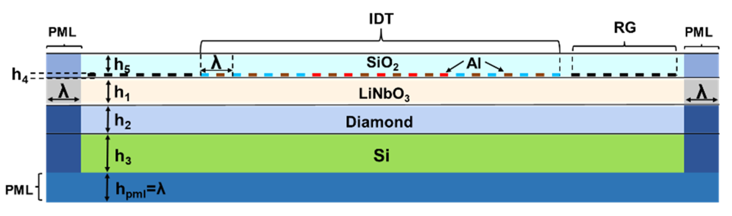
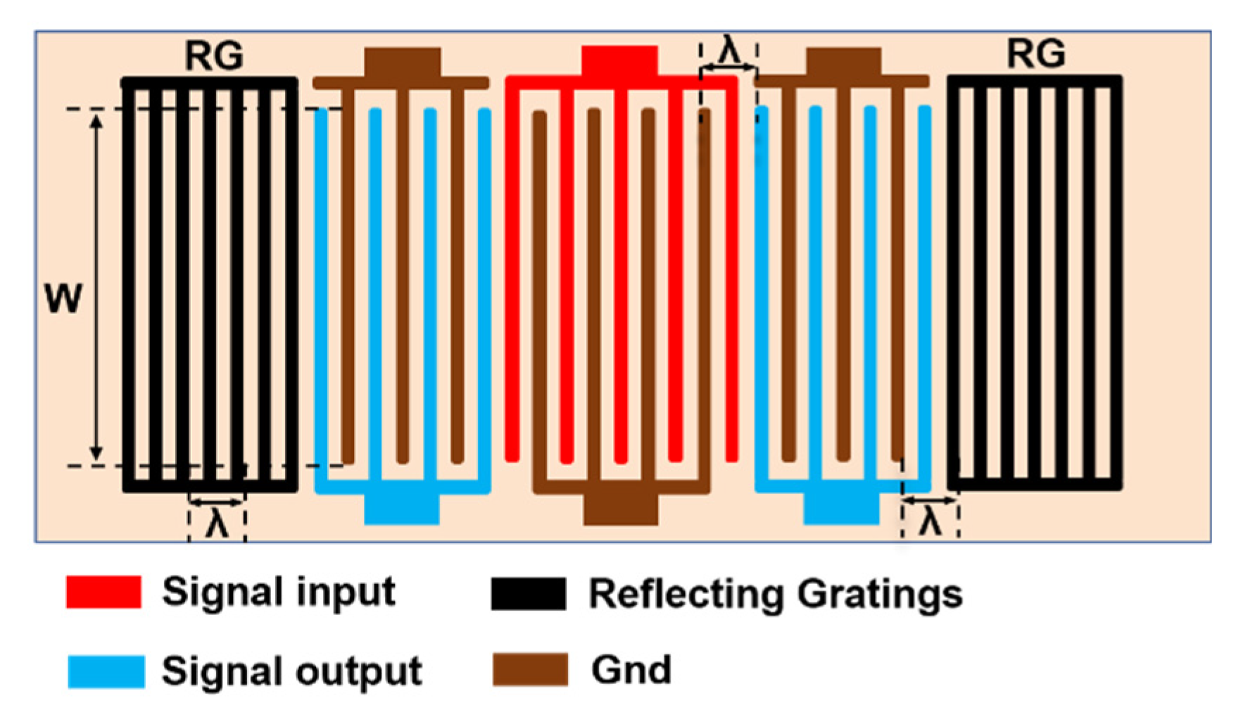
SiO2 thin film can be used as temperature compensation layer to achieve high temperature stability of SAW filter. Figure 1 displays a schematic representation of the SiO2/IDT/LiNbO3/diamond/Si structure considered in the modeling, and the structure of the LCRF in this design is shown in Figure 2. It is clear that the LCRF is suitable for obtaining SAW filters with a wide bandwidth and low insertion loss.
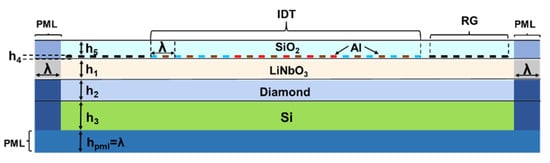
Figure 1.
Schematic representation of the SiO2/IDT/LiNbO3/diamond/Si multilayer structure.
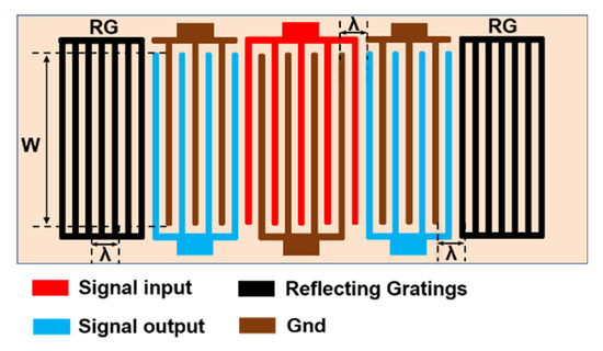
Figure 2.
IDT design of the LCRF used in this study.
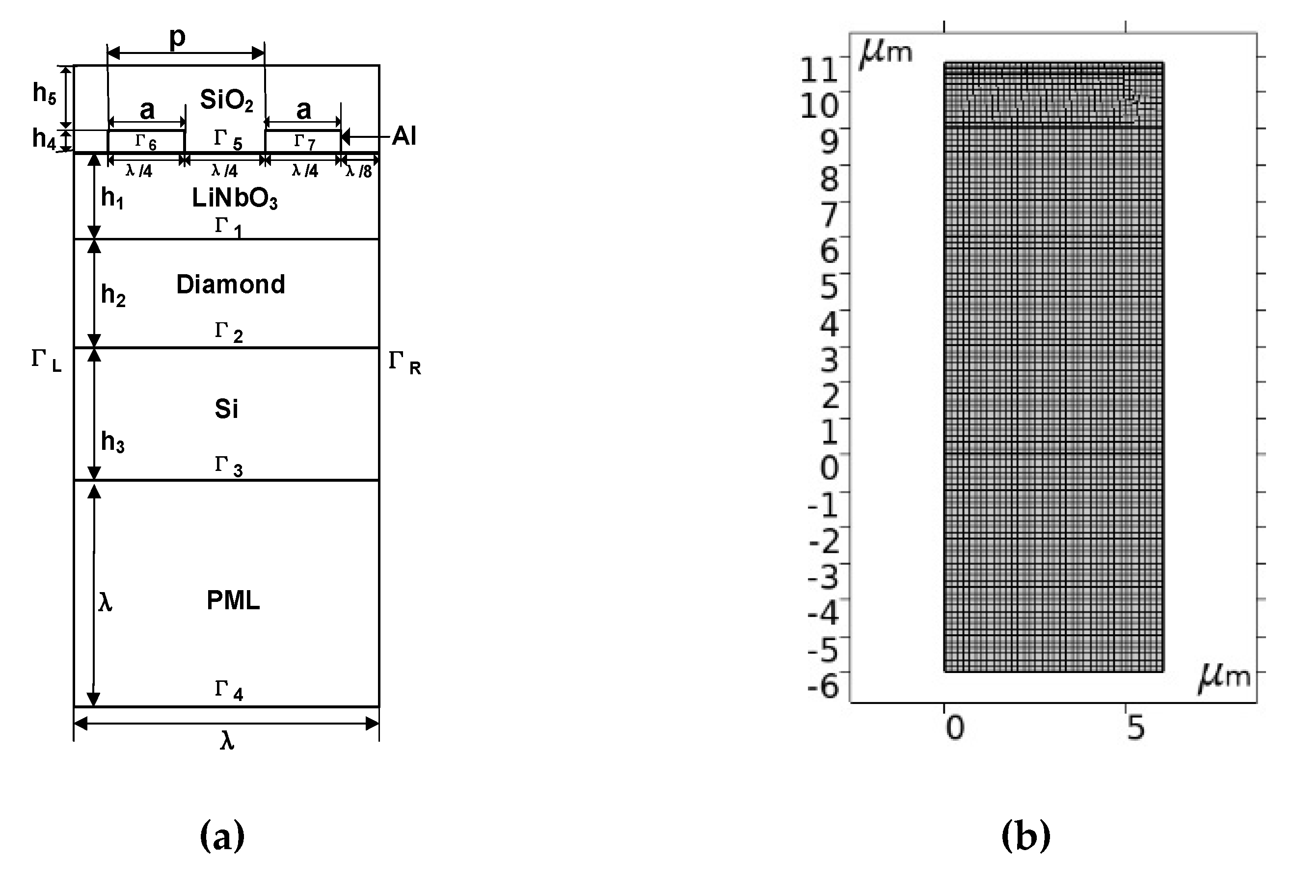
FEM simulation is an essential step in the design and fabrication of SAW devices. The device simulation can not only improve design accuracy, but it can also reduce unnecessary material losses. In this article, the software used for FEM analysis is COMSOL Multiphysics 5.6, which can easily perform piezoelectric coupling analysis and is used to analyze the response of 2D or 3D structural devices to changes in voltage and mechanical load. Thus, this software is suitable for the analysis and simulation of SAW devices. The simulation results can be used as the reference for the design and optimization of future SAW devices [11]. Because the interdigital electrodes of the IDT are periodically distributed, which reduces the simulation time, a simulation model can be established through one cycle. Considering that the Rayleigh wave and its higher-order mode vibrations are mainly limited to one wavelength (λ) on the surface, a 2D unit model with a substrate thickness greater than 1.5λ was established, as shown in Figure 3.

Figure 3.
(a) Schematic representation of the studied structure in the model. (b) Single pair IDT model meshing, quadrilateral elements = 3675.
In Figure 3a, p is the distance between two adjacent metal electrodes; a is the width of the metal electrode; and , , , , and indicate the thicknesses of the lithium niobate, diamond, silicon, metal, and SiO2 layers, respectively. To eliminate the influence of the metallization rate and obtain the maximum reflectivity of the reflector, the metallization rate (MR = a/p) was designed to be 0.5. After the metallization rate was determined, because the propagation characteristics of the layered SAW structure are independent of the wavelength, the SAW wavelength was designed to be λ = 6 μm. Because most of the energy of the SAW is confined to the surface, and the thicknesses and are excluded, it was set to a fixed value while , , and were designed as variables. An aluminum electrode with a wavelength of 6 μm was deposited on the LiNbO3 surface. Silicon is assumed to be a semi-infinite substrate. The film thickness ratios and had ten values in the range of 0.1 to 1 with the interval of 0.1, and had five values in the range of 0.1 to 0.5, with the interval of 0.1. A perfectly matched layer (PML) can absorb propagating waves, accelerate the attenuation of evanescent waves, and perfectly match arbitrary lossy media [12]; therefore, a PML of 1λ was set in this study. In COMSOL, the model needs to be meshed. As shown in Figure 3b, to ensure calculation accuracy, we divided the minimum free quadrilateral unit, the smallest unit being 1.26 nm. For the IDT structure, NG, NIN, and NOUT indicate the number of reflective gratings, input fork index, and output fork index, respectively. The specific geometric parameters involved are shown in Table 1.

Table 1.
Geometric parameters for design.
2.3. Material Parameters in the Model
The materials used in the finite element simulation included aluminum, lithium niobate, diamond, silicon dioxide, and silicon. The main characteristic parameters of materials [13,14,15,16,17,18,19,20] are shown in Table 2.
Table 2.
Material constants used in the simulations.
2.4. Setting of Boundary Conditions
In order to make the simulation results more accurate and reduce the amount of simulation calculations, the modal analysis of the layered LCRF is generally performed using a pair of interdigitated electrodes with periodic boundary conditions. The detailed electrical and mechanical boundary conditions of the numerical model are listed in Table 3.
Table 3.
Boundary conditions of the model.
3. Performance Impact Analysis
3.1. Modal Analysis
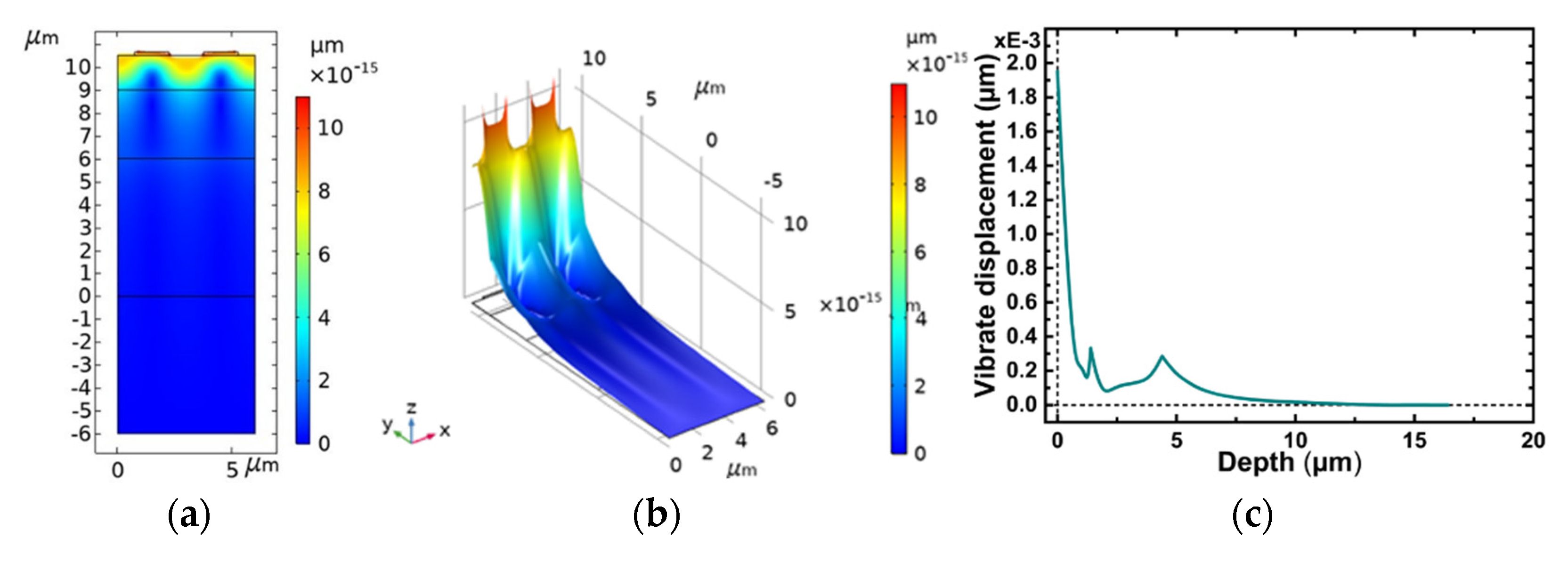
The finite element analysis of the SiO2/IDT/LiNbO3/diamond/Si layered unit structure was carried out with COMSOL Multiphysics software, and the COMSOL Multiphysics model used in this work was built in 2D Structural Mechanics Module, with emphasis on the analysis of its resonance mode and frequency response. Through the modal analysis, symmetrical modes and antisymmetric modes can be obtained, and the occurrence of their resonant frequency and anti-resonant frequency is caused by the effect of metal electrode [21]. Plots of the longitudinal displacement versus substrate depth are shown in Figure 4a,b. The results indicate that the more it approaches the surface, the greater the vibration energy of the SAW, and the more obvious the vibration. Figure 4c clearly shows that the vibration intensity decreases exponentially as the depth of the substrate increases. It can be seen that most of the vibration energy during Rayleigh waves propagation on the substrate is within one wavelength, which is consistent with the research in the literature [22]. The results demonstrate the reliability of the model.

Figure 4.
Plot of the displacement versus substrate depth of the proposed device at Rayleigh mode. (a) is a two-dimensional result and (b) is a three-dimensional result (c) is the calculated displacement of acoustic waves in depth direction.
According to the working principle of the SAW filter, the SAW excited by the IDT can be regarded as the superposition of multiple pairs of IDT excitation signals. When the finger distance p is an integer multiple of the SAW half-wavelength λ/2, the IDT can superimpose the largest excitation signal. Therefore, the relationship between the intrinsic frequency of the SAW and p can be obtained as follows [23]:
where is the phase velocity of sound wave, is the central frequency of the SAW device. The propagation velocity of SAW can be given by:
The electromechanical coupling coefficient can be calculated by the following formula [24]:
The TCF is obtained by substituting the phase velocity calculated at temperature T and T0 = 25 °C for in the following equation:
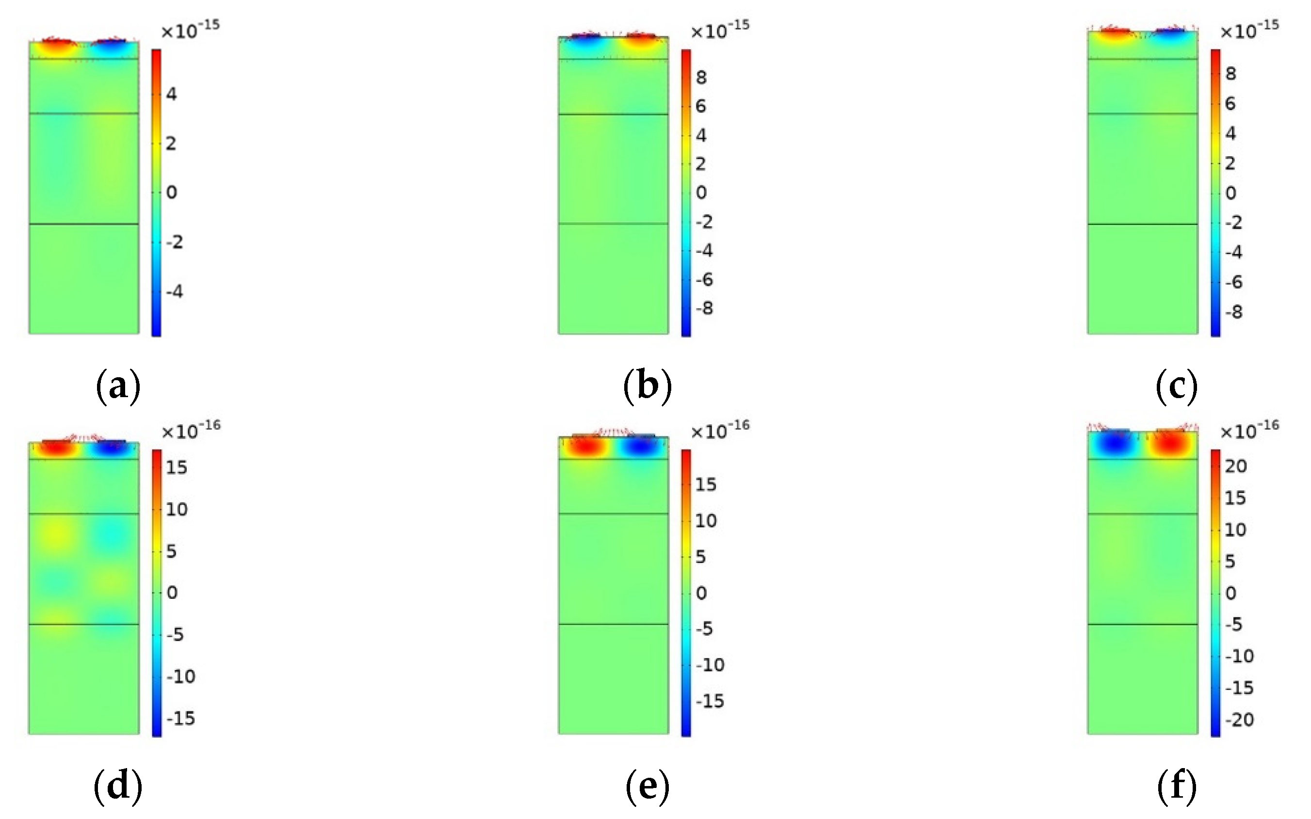
Because the acoustic velocity of the diamond substrate is higher than that of the LiNbO3 piezoelectric film, multiple modes such as Rayleigh, Sezawa, and high-order Sezawa modes coexist in the same layered structure. First, we built the LiNbO3/diamond/Si model to precisely determine the acoustic wave propagation properties on this layered structure. The Rayleigh and Sezawa anti-symmetric resonant modes of the X-displacement component of the 2D unit structure when the piezoelectric film thickness ratio () is 0.6, 0.8, and 1.0, respectively, are presented in Figure 5. The results show that in response to the increase in LiNbO3 thickness, the Rayleigh mode exhibited the largest displacement due to particle displacement close to the free surface. As the order of the mode increased (Sezawa), the magnitude of the particle displacement decreased. The Rayleigh vibration mode had a larger amplitude than the Sezawa mode, and the amplitude declined with a depth quicker than that observed in the Sezawa mode because the Rayleigh wave energy is mainly concentrated on the surface, whereas the Sezawa wave energy is distributed in the base. In addition, as the thickness of the piezoelectric layer increased, the SAWs were increasingly confined near the surface.
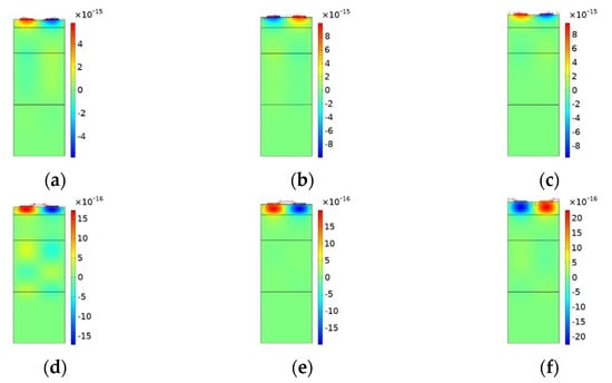
Figure 5.
The acoustic wave modes shapes and their X-component of displacement (). (a–c) Anti-resonance of Rayleigh mode. (d–f) Anti-Resonance of Sezawa mode. (a,d) When . (b,e) When and (c,f) when .
3.2. Analysis of Surface Acoustic Wave Propagation Characteristics
The performance of a SAW device with a multilayer film structure is not only affected by the electrode structure of the transducer and the characteristics of the piezoelectric material, but also related to the thickness of the piezoelectric film and the thickness of the interdigital electrode. In the layered structure, the SAW is a dispersive wave, and the acoustic parameters are dispersive, as determined by the thickness ratio of the piezoelectric and other films to the wavelength of the acoustic wave. Therefore, setting appropriate geometric parameters can significantly improve the performance of SAW devices. To obtain the best performance structure, a detailed simulation analysis was performed on the thickness of the interdigital electrode, piezoelectric layer, and temperature compensation layer. First, we studied the effects of the metal electrode and piezoelectric film on the propagation characteristics of SAWs in the IDT/LiNbO3/diamond/Si structure and then investigated the influence of thickness variation of the piezoelectric layer and thermal compensating layer on the key performance parameters of the LCRF in the SiO2/IDT/LiNbO3/diamond/Si structure.
3.2.1. Effects of Electrode Film Thickness on SAW Propagation Characteristics
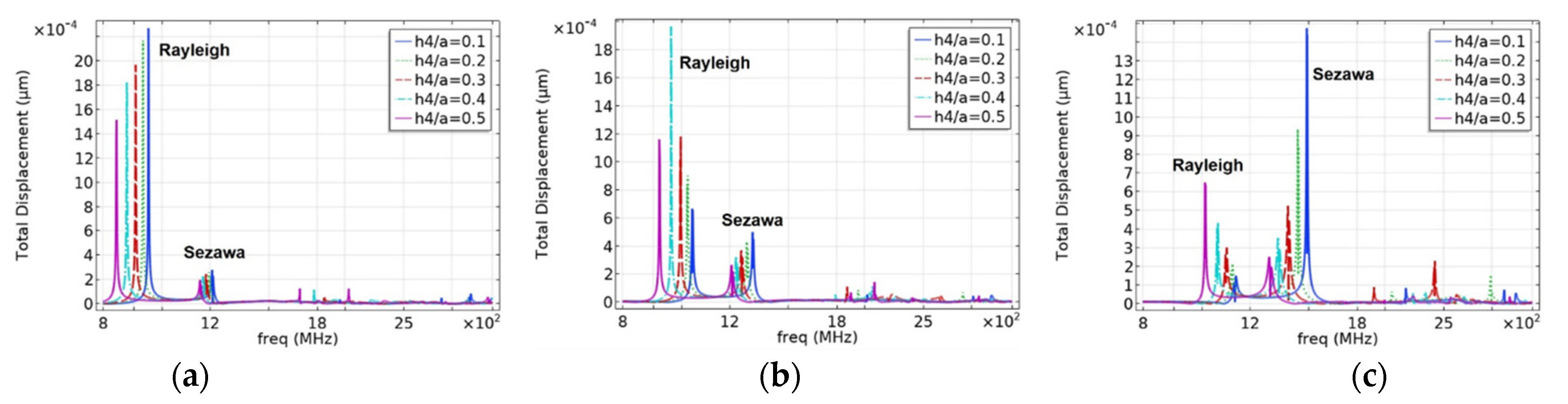
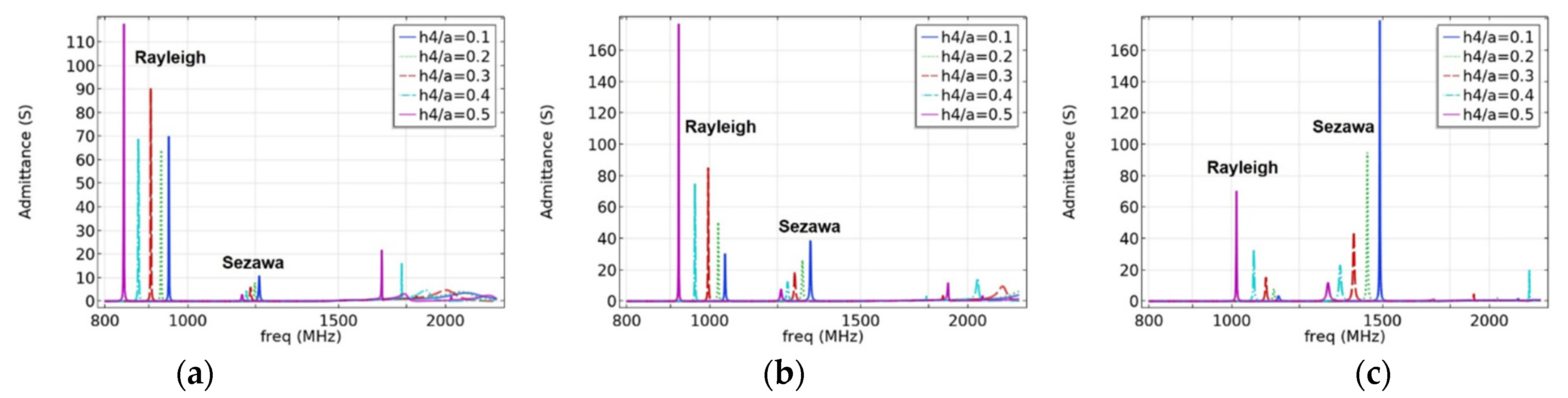
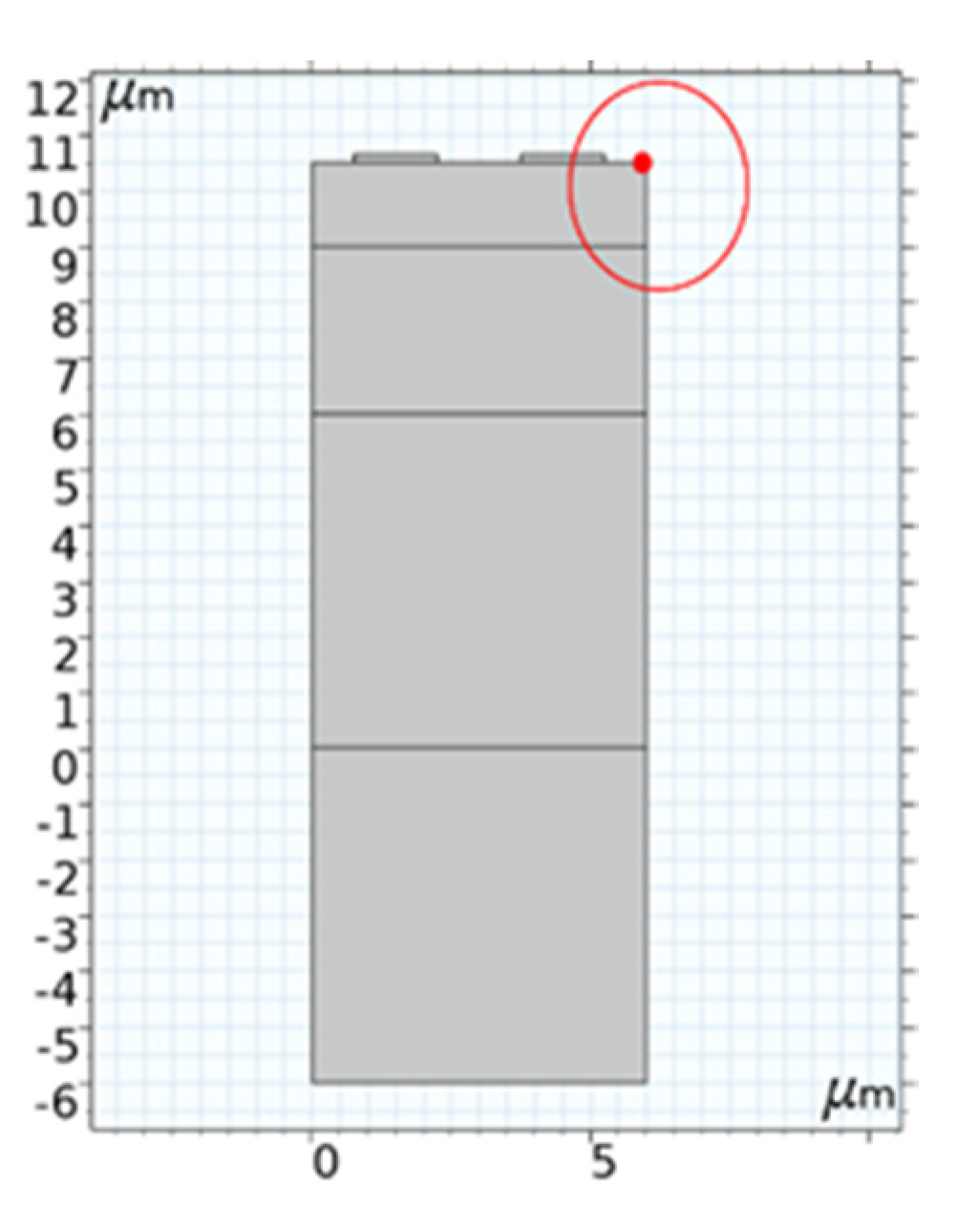
The mass loading effect of the metal electrode will be introduced when the surface of piezoelectric medium is covered with metal film [25]. To study the implications of interdigital electrodes on the SAW propagation characteristics, the resonant displacement and admittance under different electrode film thickness ratios () were compared and analyzed, as presented in this section. In this design, the surface source (I-F) structure excitation was adopted, and the substrate was assumed to be a semi-infinite substrate. To eliminate the interference of other layer thicknesses, we set the values of to 0.6, 0.8, and 1; the other structural parameters are listed in Table 1. Figure 6 shows the simulation results of the frequency characteristics of different electrode thickness ratios , and Figure 7 shows the effect of different electrode thicknesses on the admittance characteristics. It should be noted that the results in Figure 6 were probed at the red dot shown in Figure 8.
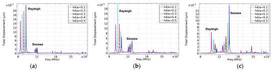
Figure 6.
The effect of electrode thickness on resonant displacement. (a) When . (b) When and (c) when .
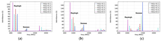
Figure 7.
The effect of electrode thickness on admittance. (a) When . (b) When and (c) when .
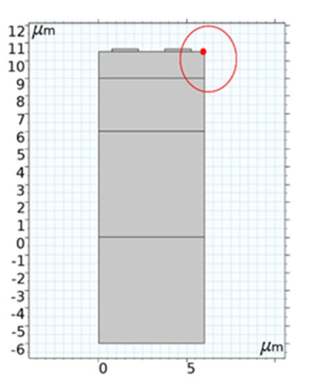
Figure 8.
Position of total displacement probe.
As shown in Figure 6a, as the electrode thickness decreases, the resonance frequency and displacement of the Rayleigh and Sezawa waves gradually increase, and the electrode mass loading effect is apparent. When , that is, , the resonance frequency and displacement reach their maximum values. In other cases, the resonance displacement in the Rayleigh wave decays as the electrode thickness decreases, as shown in Figure 6b,c. In contrast, as the thickness of the piezoelectric layer decreases, the influence of the electrode thickness on the Sezawa wave increases, and the Sezawa mode shows strict regularity. The variation rules of the results in Figure 7 are consistent with those in Figure 6. In either case, the resonance frequency decayed with an increase in the electrode thickness. There are other types of waves in the high-frequency range, but they were not considered in this study because of their small influence.
For a unit model with fixed 1.5 μm LiNbO3 layer thickness, the phase velocities of the Rayleigh mode and Sezawa mode drop with increasing electrode thickness, while exhibits a rising trend (plotted in Figure 9).
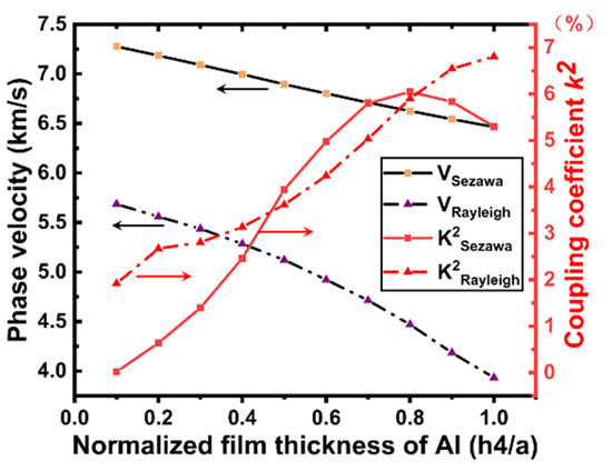
Figure 9.
and dependence on (when = 1).
As shown in Figure 9, the phase velocities decrease with the increasing electrode thickness for all wave modes. The phase velocity changes from 5686 to 3994 m/s for Rayleigh and from 7277 m/s to 6484 m/s for Sezawa. This indicates that the phase velocity of the Rayleigh wave decreases rapidly with an increase in the electrode thickness, whereas the phase velocity of the Sezawa wave is less affected by the electrode thickness. Moreover, this difference confirms that Rayleigh waves are concentrated on the surface of the piezoelectric thin film. In addition, it is clear that both the Rayleigh and Sezawa modes have a large value, exhibiting an upward trend for both. A high value (greater than 5.75%) was obtained for Sezawa in the range of 0.5–0.8, and the value peaked at = 0.8.
When the electrode thickness is zero or very small, the resonant and anti-resonant frequencies are basically the same, but with an increase in the electrode thickness, the Rayleigh wave acoustic field begins to move to the surface of the piezoelectric layer; the resonant and anti-resonant frequencies become significantly different and, according to Formula (7), correlate with the corresponding . Simultaneously, the acoustic field of the Sezawa wave is mainly distributed at the interface between the piezoelectric film and the substrate; therefore, the mass loading effect of the electrode has a limited contribution to the velocity of the Sezawa wave. As the electrode thickness increased, the sound field began to move toward the surface of the piezoelectric layer. In this process, the distributions of the sound field and the electric field begin to match, and when the electrode thickness reaches a certain value, can reach the maximum value. As the thickness of the electrode continued to increase, the acoustic energy began to concentrate inside the electrode. At this time, the acoustic and electric fields begin to mismatch, and the coupling coefficient begins to decrease. Comparing the results presented in Figure 6, Figure 7 and Figure 9, when = 0.1, it can be observed that these SAWs have the highest sound velocity, a good coupling coefficient, and significant admittance characteristics. Therefore, this electrode parameter was used in the subsequent studies.
3.2.2. Effects of Piezoelectric Layer Thickness on SAW Propagation Characteristics
The characteristics of SAWs in piezoelectric multilayer media are not only affected by the characteristics of the piezoelectric layer material but also depend on the thickness of the piezoelectric layer. Initially, to validate our simulation method for the SiO2/IDT/LiNbO3/diamond/Si structure, we first used the IDT/LiNbO3/diamond/Si structure. In the next stage of the study, a thin film of SiO2 was coated over the surface of the LiNbO3 film, and the resonance frequencies of both modes with different thicknesses of the LiNbO3 film were recorded. The other structural parameters are listed in Table 1.
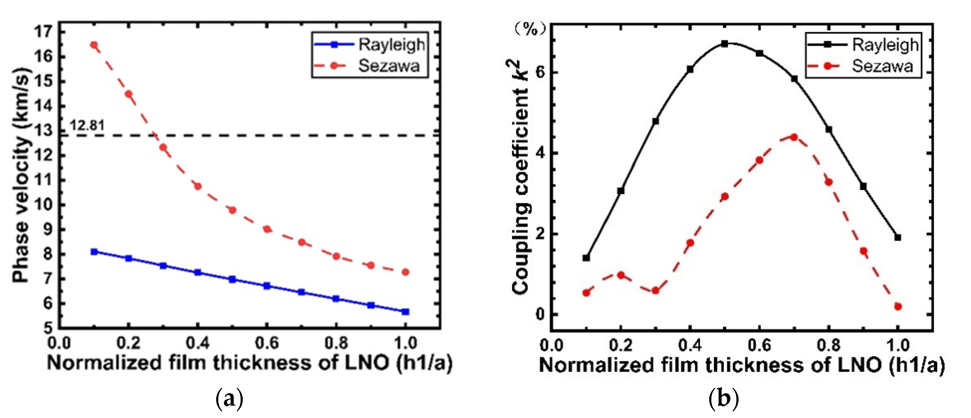
The simulation results for the propagation characteristics of the IDT/LiNbO3/diamond/Si structure are presented in Figure 10. The phase velocity of the Rayleigh mode decreases with increasing normalized LiNbO3 film thickness, whereas that of the Sezawa mode decreases more dramatically. As displayed in Figure 10a, the value of the phase velocity changes from 8110 to 5660 m/s in the Rayleigh mode, and the value of the phase velocity changes from 16.48 to 7.28 km/s. When is less than 0.3, the Sezawa wave velocity is larger than that of the diamond shear wave (12.81 km/s). Meanwhile, the Sezawa wave will leak energy to the diamond substrate, thus increasing the insertion loss. As shown in Figure 10b, for the Rayleigh wave, first increases with an increase in , reaches the maximum value of 6.71% when = 0.5, and then starts to decrease with a further increase in .
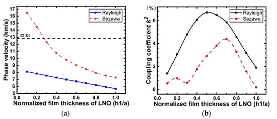
Figure 10.
(a) SAW velocity versus normalized thickness of LiNbO3 in SiO2-free structure; (b) Electromechanical coupling coefficient versus normalized LiNbO3 thickness in SiO2-free structure.
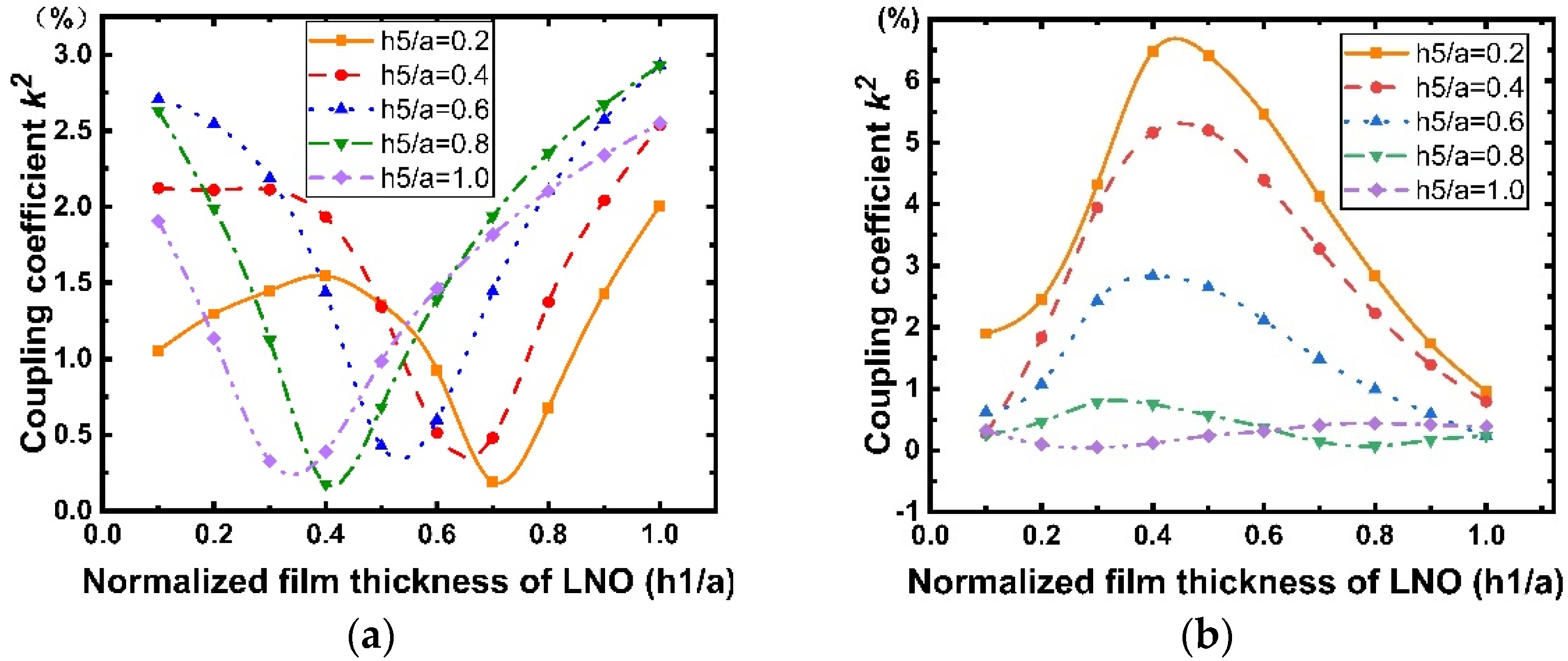
Figure 11 shows the dispersion curves of the phase velocity calculated for the Rayleigh and Sezawa modes with when the values of are 0.2, 0.4, 0.6, 0.8, and 1. According to Figure 11a,b, we can observe that the velocities of the Rayleigh and Sezawa waves decrease as and increase. This behavior is explained by the fact that the elastic velocity in the structure is close to that of the diamond substrate when the LiNbO3 and SiO2 layers are very thin, and these values decrease to reach those of the piezoelectric film. In the Sezawa mode, a high of 11.59 km/s could be obtained at = 0.1 in the Sezawa mode; as , a higher will result in a higher frequency, which is beneficial for high-frequency device fabrication and performance. Figure 12 shows the calculated LiNbO3 thickness dependence of . It is interesting that, in the Rayleigh wave mode (Figure 12a), shows the opposite trend and decreases dramatically compared with that for the structure without SiO2. In contrast, the Sezawa mode (Figure 12b) presents the same trend as before, and the value of increases significantly when the SiO2 thickness is small. In particular, when = 0.4, the maximum coupling coefficient of this mode is 6.47%.
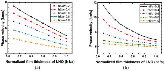
Figure 11.
Dispersion curves of the Rayleigh and Sezawa waves velocity calculated for various values of for the structure SiO2/IDT/LiNbO3/diamond/Si. (a) Rayleigh mode; (b) Sezawa mode.
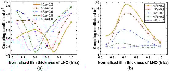
Figure 12.
Dispersion curves of the Rayleigh and Sezawa waves electromechanical coupling coefficient () calculated for various values of for the structure SiO2/IDT/LiNbO3/diamond/Si. (a) Rayleigh mode; (b) Sezawa mode.
3.2.3. Effects of Temperature Compensation Layer Thickness on SAW Propagation Characteristics
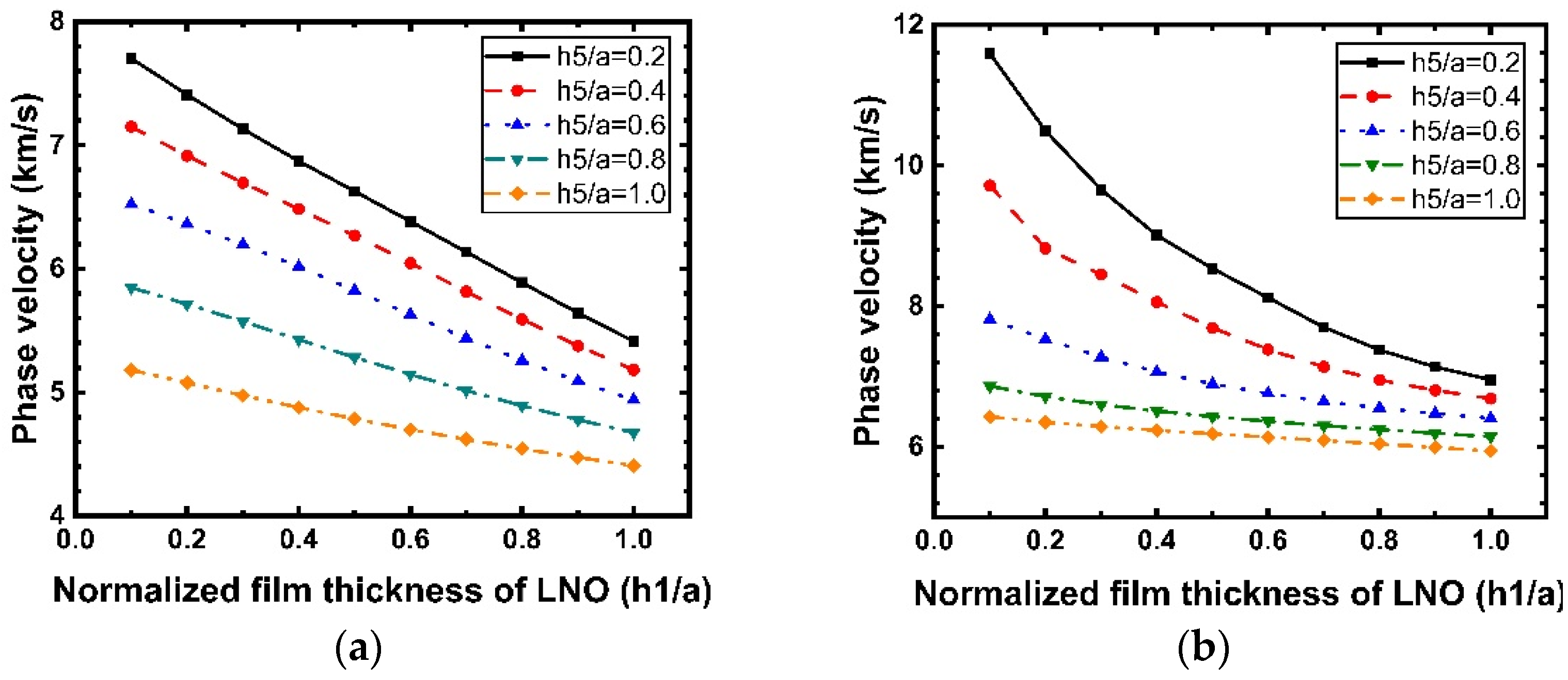
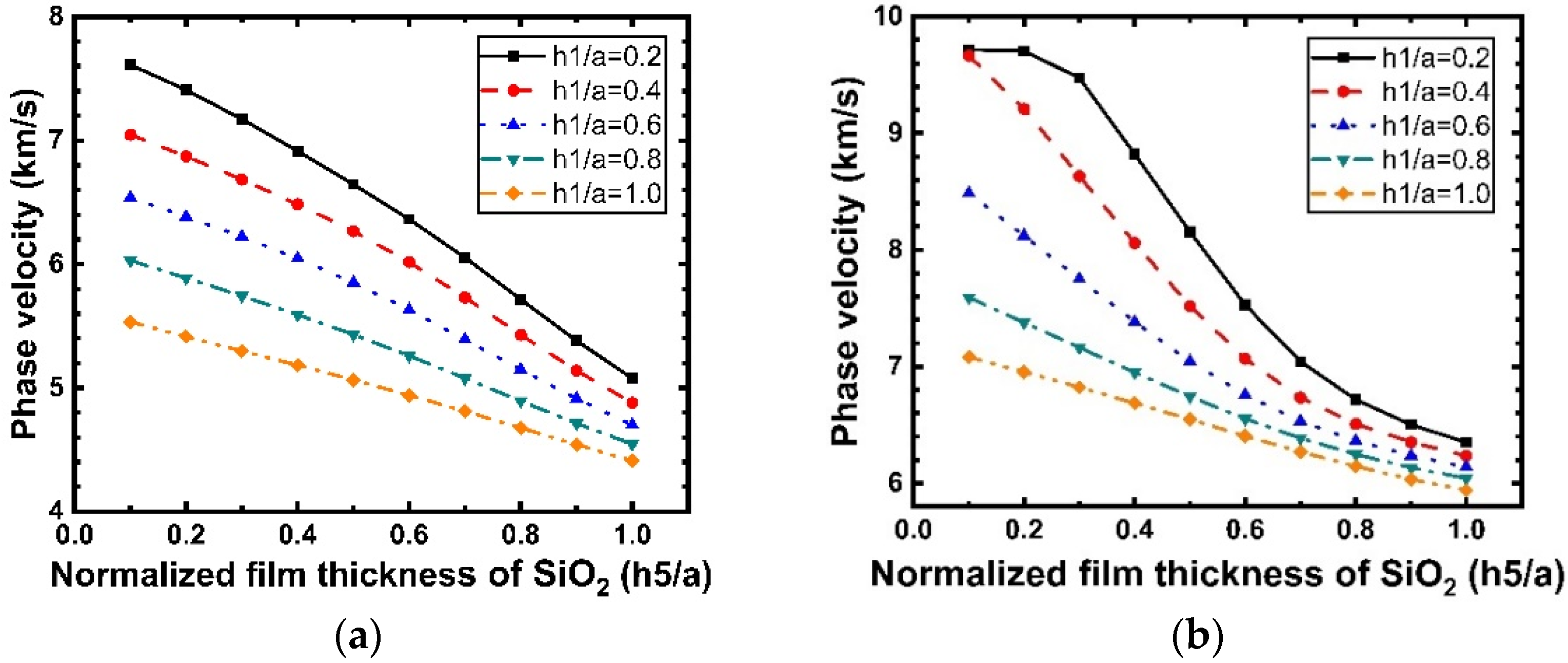
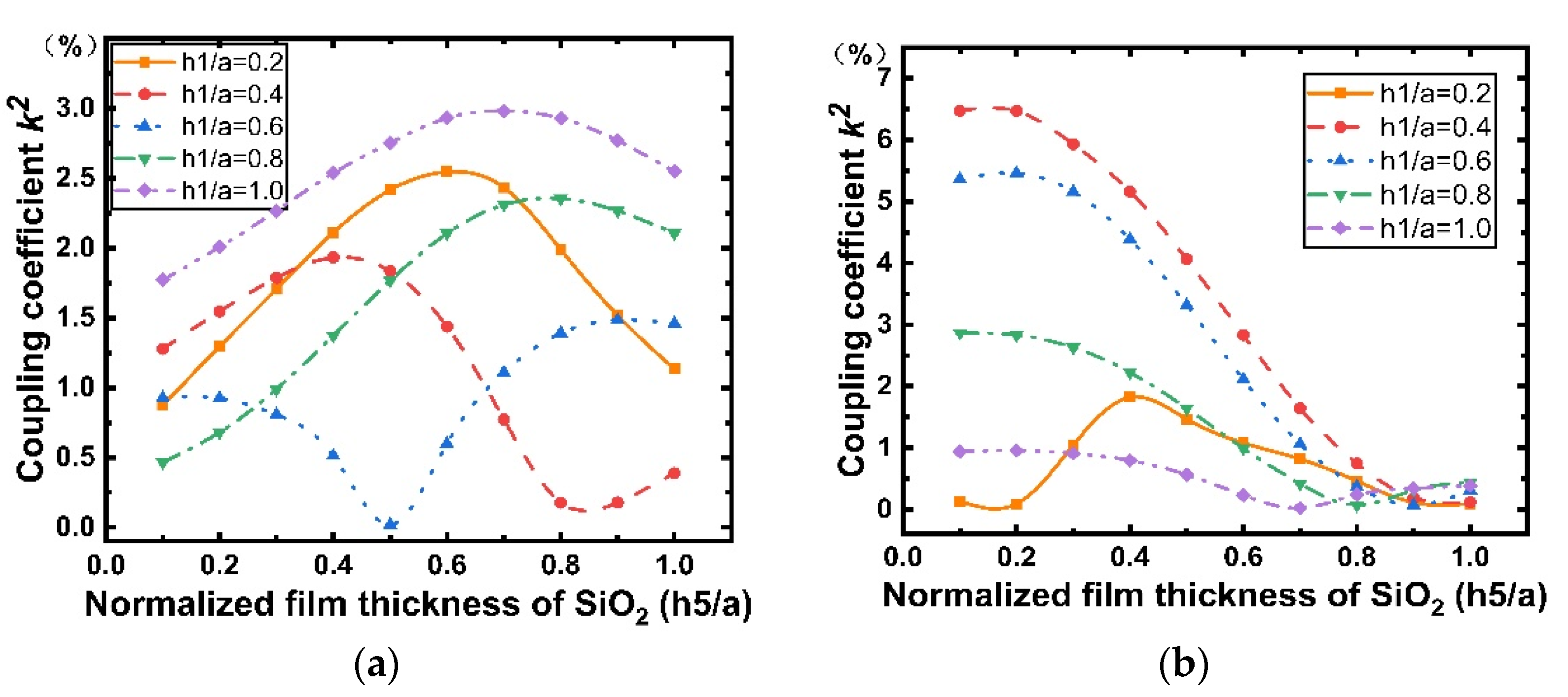
To study the implications of SiO2 on SAW propagation, different thicknesses of SiO2 were considered, and the results are shown in Figure 13 and Figure 14. Similarly, five different LiNbO3 thicknesses were used for comparison. From Figure 13, we can observe that although the thickness of the piezoelectric layer differs, the phase velocities of the Rayleigh wave and Sezawa wave in the five cases all decrease with the increase in the thickness of the SiO2 cover layer, where the SAW velocity slows down with increasing thickness of the SiO2 films because the SAW velocity in SiO2 is smaller than that in the IDT/LiNbO3/diamond/Si structure and the acoustic energy starts confining more in the SiO2 layer. In addition, according to Figure 14, when the thickness of the SiO2 layer is very small and increases, of the Sezawa wave increases and reaches the maximum (6.47%) at . In contrast, in Figure 14a, it is observed that of the Rayleigh wave mode is generally lower than that of the Sezawa one but is still much higher than of the AlN/diamond structure [26]. Therefore, we can achieve a maximum value of by varying the thickness of the SiO2 layer deposited on the electrode. As expected, the SiO2 layer deposited in the electrode gap increases the electrostatic capacity of the device, thus reducing the maximum of the device without the SiO2 layer.
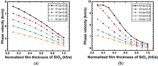
Figure 13.
Dispersion curves of the Rayleigh and Sezawa waves velocity calculated for various values of for the structure SiO2/IDT/ LiNbO3/diamond/Si. (a) Rayleigh mode; (b) Sezawa mode.
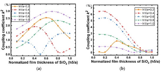
Figure 14.
Dispersion curves of the Rayleigh and Sezawa waves electromechanical coupling coefficient () calculated for various values of for the structure SiO2/IDT/LiNbO3/diamond/Si. (a) Rayleigh mode; (b) Sezawa mode.
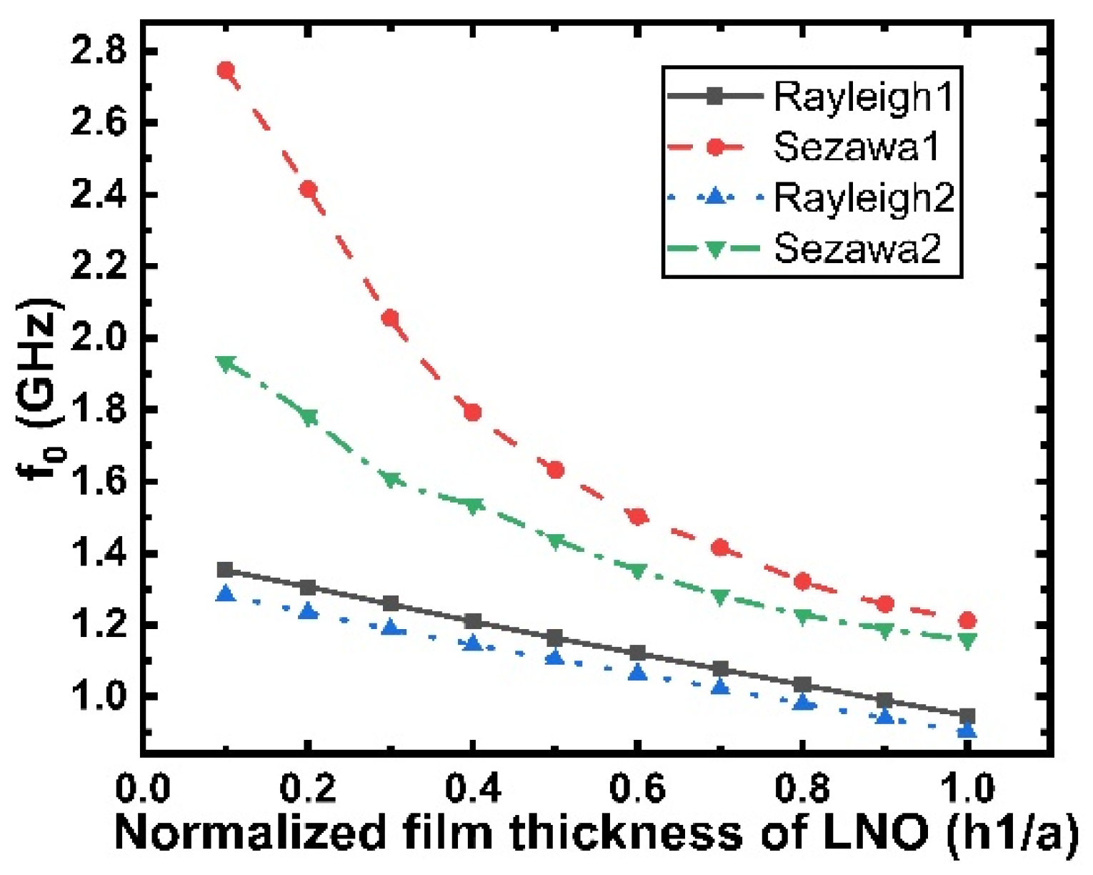
Figure 15 shows the central frequency () dependence on for the Rayleigh and Sezawa modes. It is clear that the center frequency of Sezawa mode is greatly affected when the SiO2 layer is covered, and correspondingly, the center frequency of Rayleigh mode is less affected. For both wave modes, the acoustic wave central frequency reduces with the increasing LiNbO3 layer thickness. However, within this range, the Rayleigh and Sezawa modes can still maintain high frequencies above GHz, so the layered structure still has a great advantage. These characteristics make this material system superior for high-frequency wideband applications.
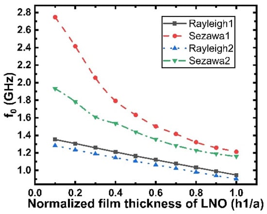
Figure 15.
Plot of central frequency versus normalized LiNbO3 thickness (). Rayleigh1, Sezawa1, and Rayleigh2, Sezawa2 are the two SAW modes before and after the layer thickness = 0.1 is added, respectively.
The influence of temperature on the SAW devices has two main aspects: one is that thermal expansion of the SAW device structure causes the resonance frequency to change; additionally, temperature changes the material parameters. Under the influence of temperature, the material parameters in Equations (1)–(4) differ, where becomes and becomes . Here, only the first-order temperature coefficient is considered.
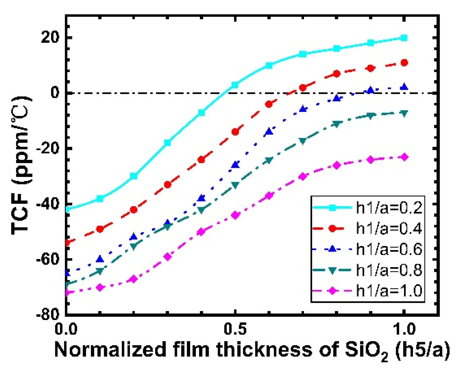
The change in material parameters leads to a change in the SAW velocity, and the TCF is obtained using Equation (8). Figure 16 shows the TCF of a Rayleigh wave propagating along SiO2/IDT/LiNbO3/diamond/Si versus the normalized thickness of the SiO2 layer with different thicknesses of the LiNbO3 layer. For 0.8 and 1, a negative value of TCF is observed for all values of SiO2 layer thickness. In the case of , 0.4, and 0.6, a positive value occurs for a large , and a TCF of zero is obtained. Note that the TCF of LiNbO3 single crystal reaches −75 ppm/°C, and it is apparent that the existence of the SiO2 film caused an improvement in the TCF. Usually, as shown in Figure 16, for a better TCF, a thicker SiO2 overcoat is preferred.
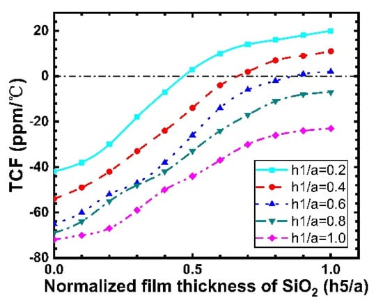
Figure 16.
Calculated TCF changes versus SiO2 thickness.
Therefore, the multilayer structure with added high-speed substrate can greatly increase not only the propagation velocity of SAWs but also the electromechanical coupling coefficient. A faster propagation velocity and larger correspond to a higher working frequency and larger bandwidth, which are more conducive to the design and manufacture of high-frequency wideband SAW devices. These results show that the TCF, working frequency, and bandwidth characteristics of SAW filters can be improved using a multilayer structure.
3.3. Transient and S Parameter Analysis
To simulate the real operation conditions of the SAW filter, the structure was analyzed in the time domain. Moreover, to reduce computational time, we modeled the SAW filter as a 2D system. In this model, , and were set to 0.7, 0.1, and 0.2, respectively. In this case, the eigenfrequency of the periodic model is MHz, and the corresponding speed of the Rayleigh wave is = 6138 m/s. Figure 17 shows the total deformation of the system at the eigenfrequency of the simulation. The results indicate that the layered structure can lead to a confinement of the acoustic energy in the surface multilayer area. Further, this multilayered structure suppresses the bulk wave radiation and enables SAW energy confinement in the surface area, which is expected to improve the Q-factor.
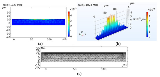
Figure 17.
Simulation diagram of the total surface displacement of the model. (a) is a two-dimensional result and (b) is a three-dimensional result; (c) is the mesh density profile of complete structure, quadrilateral elements = 14319.
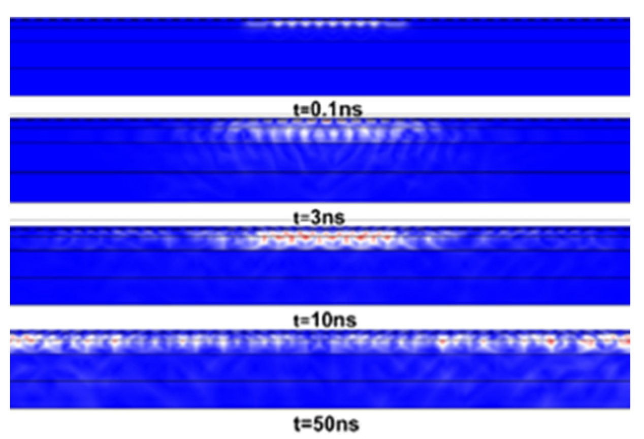
The transient simulation was run for 50 ns with the timestep of 0.1 ns. Figure 18 shows the propagation characteristics of SAWs when the loading of the SAW filter is the harmonic electric voltage on the input IDT with an amplitude of 10 V and frequency equal to the eigenfrequency computed in the modal analysis, MHz. As shown in Figure 18, the waves propagate on the surface of the filter, but some of them also propagate into the substrate, and at approximately t = 3 ns, the SAWs reach the output electrode.
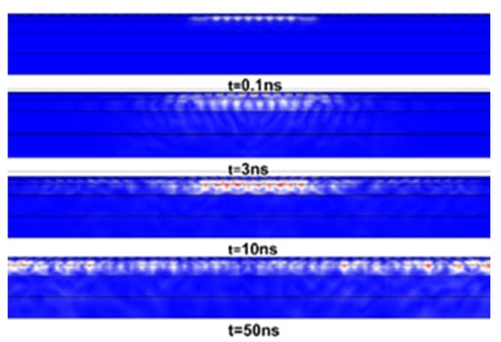
Figure 18.
Simulation diagram of surface acoustic wave propagation in the structure.
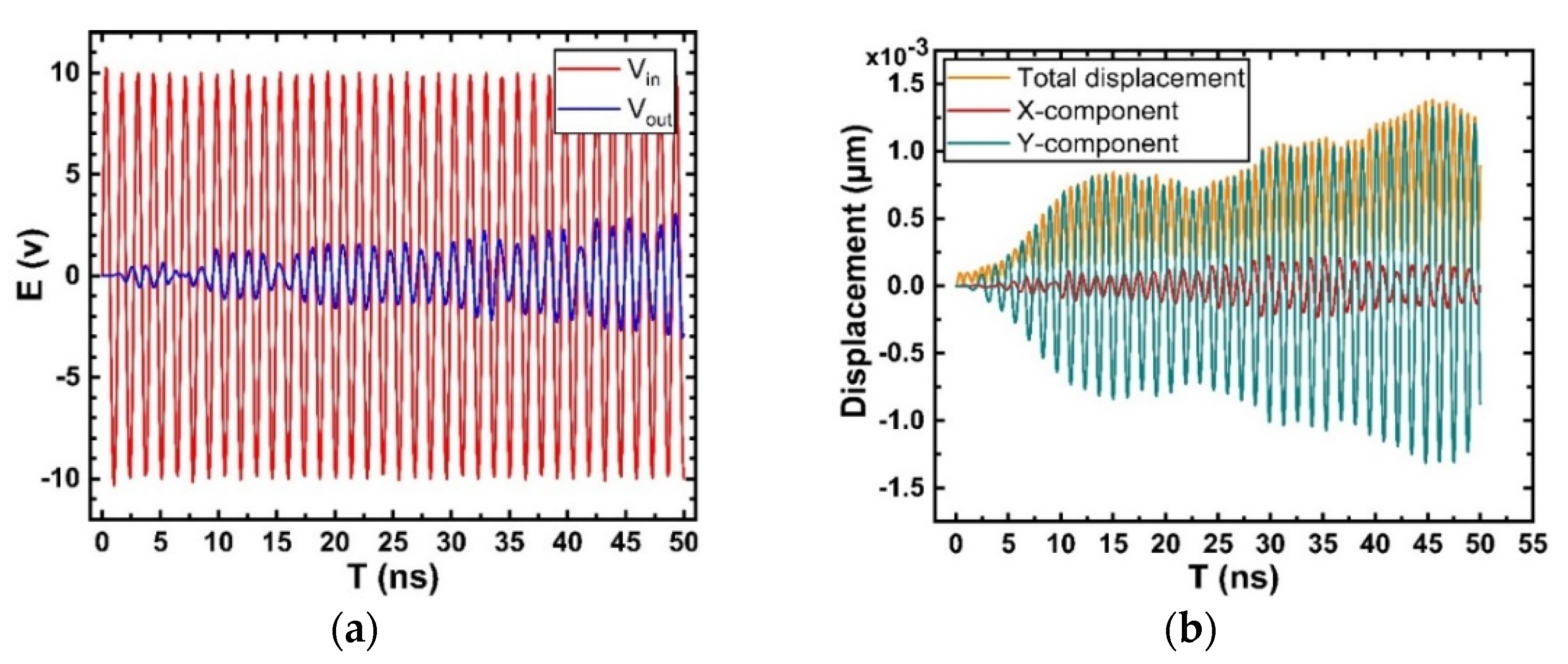
Figure 19a shows input and output voltage on IDT as a function of time. The input signal is harmonic from start of simulation, but the output IDT needs some time to receive Rayleigh waves. The result is consistent with Figure 18.
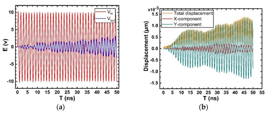
Figure 19.
Results of transient analysis. (a) Input and output voltage on IDT; (b) Simulation diagram of the total surface displacement of the model and its X-Y component displacement.
Figure 19b shows the total displacement of the system and its X-Y component displacement changes in the time-domain simulation. The displacement direction of the Rayleigh wave has two components that are perpendicular and parallel to the surface. The particle vibration on the upper surface takes an elliptical path with two parts. It can be seen from Figure 19b that after a delay of 2 ns, the output begins to exhibit a significant vibration displacement. The displacement in the X direction lags slightly behind that in the Y direction, and the amplitude of the Y component is higher than that of the X component. This is because the crystal structure in the infinite base direction vibrates easier than that in the restricted direction, and the amplitude of the particle in the Y direction is greater than that in the X direction.
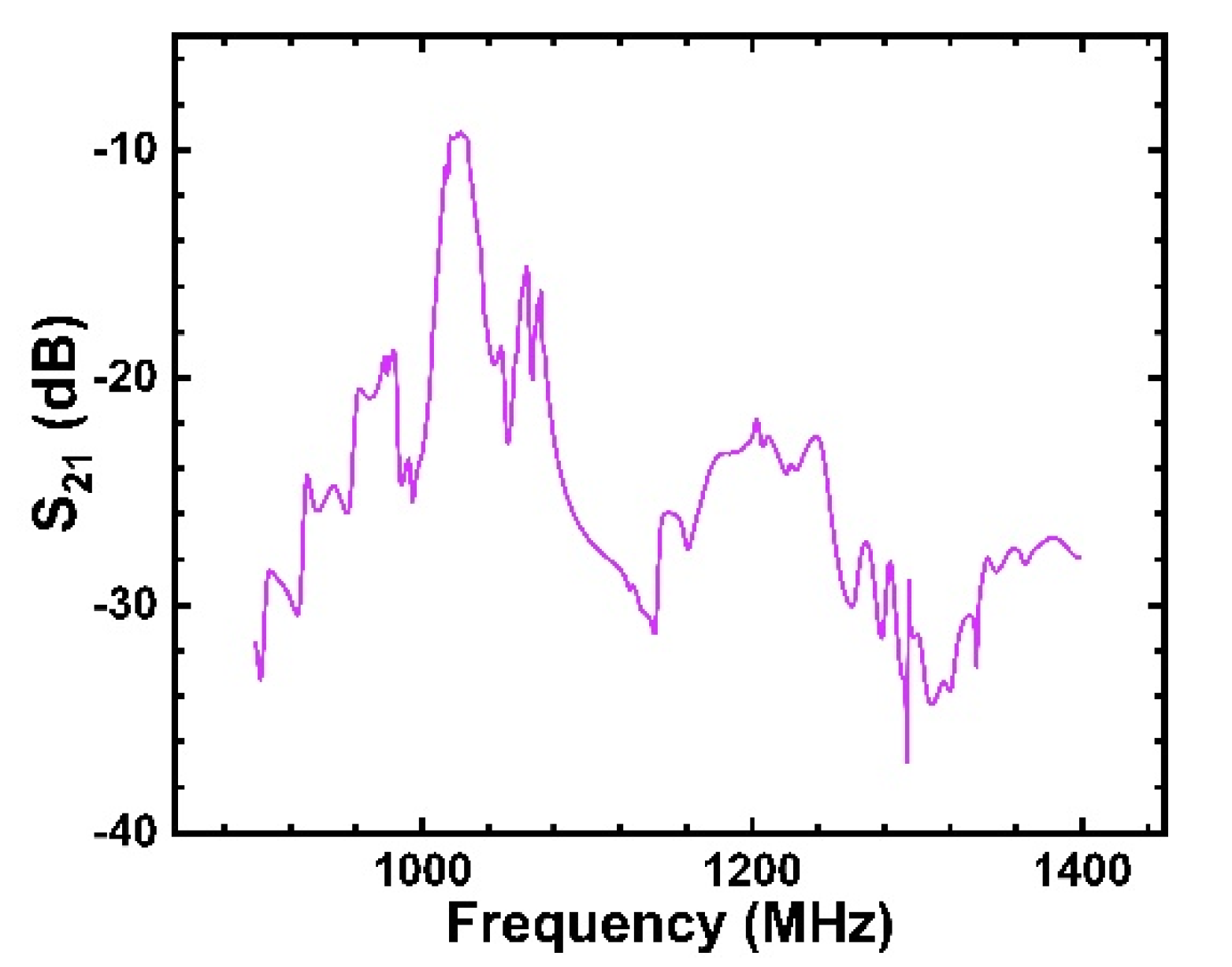
Figure 20 shows the S21 characteristics in the frequency domain analysis of the filter designed with the SiO2/IDT/LiNbO3/diamond/Si structure. It can be seen that the transmission characteristics of the device are the best at the center frequency MHz, and the minimum insertion loss is less than 10 dB. However, for the low-loss filter, there was still a large insertion loss. This is because this design parameter cannot obtain the optimal , which leads to excessive insertion loss, and the insertion loss can be further reduced using the geometric result of a high .
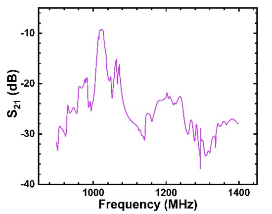
Figure 20.
S21 characteristics of SAW filter of SiO2/IDT/LiNbO3/diamond/Si structure with Rayleigh mode.
SAW parameters of SiO2/IDT/LiNbO3/diamond/Si compared with other SAW material systems are listed in Table 4.
Table 4.
SAW parameters of SiO2/LiNbO3/diamond/Si compared with other material systems.
In contrast, SiO2/LiNbO3/diamond/Si is found to have a zero-temperature coefficient, and thus this material can be regarded as an ideal system for high-frequency wide-bandwidth applications. It is worth noting that in most of the literature, the width of the interdigital electrode reaches the submicron level; we set λ as 6 μm, and hence, the difficulty of manufacturing is reduced. If we continue to reduce its width, the operating frequency (f0) will double. For example, when λ = 1 μm, f0 exceeds 10 GHz in the Sezawa mode.
4. Conclusions
In this study, a new SiO2/IDT/LiNbO3/diamond/Si composite substrate structure designed to realize high-performance SAW devices was investigated. The effects of the thicknesses of IDT, LiNbO3, and SiO2 thin films on the structural performance were numerically evaluated using a 2D finite element model. In addition, the phase velocities, coupling coefficients, and temperature coefficients of the Rayleigh and Sezawa waves were calculated.
As a result, the layered structure was found to have a high phase velocity of up to 10 km/s and a high electromechanical coupling coefficient of 6.47% with a small temperature coefficient as low as 0 ppm/°C. Compared with those of traditional LiNbO3 single crystals, the phase velocity and electromechanical coupling coefficient of the layered structure increased by 144% and 17.7%, respectively. Furthermore, the layered structure has high temperature stability. From the results, we can conclude that the structure is promising for the realization of high-performance SAW filters at frequencies above the GHz range as long as the width of the interdigital electrode can be set reasonably. In the same way, the results provided in this study are of great importance for the future design of high-performance SAW devices on SiO2/IDT/LiNbO3/diamond/Si layered structures.
Author Contributions
Conceptualization, methodology, writing—original draft preparation, writing, and editing, H.Z.; review, supervision, validation, funding acquisition, H.W. All authors have read and agreed to the published version of the manuscript.
Funding
This research was funded by the National Key R&D Program of China, grant number (No.2018YFF01010500), the Fund for Shanxi ‘1331 Project’ Key Subject Construction (1331KSC).
Institutional Review Board Statement
Not applicable.
Informed Consent Statement
Not applicable.
Data Availability Statement
Not applicable.
Acknowledgments
The authors wish to thank the Sponsored by the National Key R&D Program of China (No.2018YFF01010500), the Fund for Shanxi ‘1331 Project’ Key Subject Construction (1331KSC), and the open project of the Key Laboratory of Dynamic Measurement (North University of China), Ministry of Education, North University of China.
Conflicts of Interest
The authors declare no conflict of interest.
References
- Kobayashi, Y.; Suchiya, T.; Okazaki, M. High-frequency surface acoustic wave resonator with ScAlN/hetero-epitaxial diamond. Diam. Relat. Mater. 2020, 111, 108190. [Google Scholar] [CrossRef]
- Kakio, S. High-performance surface acoustic wave devices using composite substrate structures. Jpn. J. Appl. Phys. 2021, 60, SD0802. [Google Scholar] [CrossRef]
- Assouar, M.B.; Elmazria, O. Modelling of SAW filter based on ZnO/diamond/Si layered structure including velocity dispersion. Appl. Surf. Sci. 2000, 164, 200–204. [Google Scholar] [CrossRef]
- Maouhoub, S.; Aoura, Y.; Mir, A. FEM simulation of Rayleigh waves for SAW devices based on ZnO/AlN/Si. Microelectron. Eng. 2015, 136, 22–25. [Google Scholar] [CrossRef]
- Wang, L.; Chen, S.M.; Zhang, J. Enhanced performance of 17.7 GHz SAW devices based on AlN/diamond/Si layered structure with embedded nanotransducer. Appl. Phys. Lett. 2017, 111, 253502. [Google Scholar] [CrossRef]
- Xie, B.W.; Ding, F.Z.; Dong, Z.B. FEM analysis of piezoelectric film as IDT on the diamond substrate to enhance the quality factor of SAW devices. Diam. Relat. Mater. 2020, 102, 107659. [Google Scholar] [CrossRef]
- Wang, Y.; Zhang, S.Y.; Fan, L. Characteristics of surface acoustic waves excited by (1120) zno films deposited on R-sapphire substrates. IEEE Trans. Ultrason. Ferr. 2013, 60, 1213–1218. [Google Scholar] [CrossRef] [PubMed]
- Wang, L.Y.; Wang, H.L. Analysis of propagation characteristics of AlN/diamond/Si layered SAW resonator. Microsyst. Technol. 2020, 26, 1273–1283. [Google Scholar] [CrossRef]
- Nikolaou, I.; Hallil, H.; Tamarin, O. A three-dimensional model for a graphene guided SH-SAW sensor using finite element method. In Proceedings of the 2016 31st Symposium on Microelectronics Technology and Devices, Belo Horizonte, Brazil, 29 August–3 September 2016. [Google Scholar]
- Hakiki, M.E.; Mohamed, O.E.; Alnot, P. Theoretical investigation of surface acoustic wave in the new, three-layered structure: ZnO/AlN/diamond. IEEE Trans. Ultrason. Ferr. 2007, 54, 676–681. [Google Scholar] [CrossRef]
- Wang, T.; Green, R.; Guldiken, R.; Wang, J. Finite element analysis for surface acoustic wave device characteristic properties and sensitivity. Sensors 2019, 19, 1749. [Google Scholar] [CrossRef] [Green Version]
- Fang, J.Y.; Wu, Z.H. Generalized perfectly matched layer-an extension of Berenger's perfectly matched layer boundary condition. IEEE Microw. Guided Wave Lett. 1995, 5, 451–453. [Google Scholar] [CrossRef]
- Kannan, T. Finite Element Analysis of Surface Acoustic Wave Resonators. Master’s Thesis, University of Saskatchewan, Saskatoon, SK, Canada, 2006. [Google Scholar]
- Maouhoub, S.; Aoura, Y.; Mir, A. FEM simulation of AlN thin layers on diamond substrates for high frequency SAW devices. Diam. Relat. Mater. 2016, 62, 7–13. [Google Scholar] [CrossRef]
- Aslam, M.Z.; Jeoti, V.; Karuppanan, S. FEM analysis of sezawa mode SAW sensor for VOC based on CMOS compatible AlN/SiO2/Si multilayer structure. Sensors 2018, 18, 1687. [Google Scholar] [CrossRef] [PubMed] [Green Version]
- Li, Q.; Qian, L.R.; Fu, S.L.; Song, C. Characteristics of one-port surface acoustic wave resonator fabricated on ZnO/6H-SiC layered structure. J. Phys. D Appl. Phys. 2018, 51, 145305. [Google Scholar] [CrossRef]
- Zhang, Z.W.; Wen, Z.Y.; Wang, C.M. Investigation of surface acoustic waves propagating in ZnO–SiO2–Si multilayer structure. Ultrasonics 2013, 53, 363–368. [Google Scholar] [CrossRef] [PubMed]
- Benetti, M.; Cannata, D.; Pictrantonio, F.D.; Verona, E. Growth of AlN piezoelectric film on diamond for high-frequency surface acoustic wave devices. IEEE Trans. Ultrason. Ferr. 2005, 52, 1806–1811. [Google Scholar] [CrossRef]
- Luo, J.T.; Quan, A.J.; Fu, C. Shear-horizontal surface acoustic wave characteristics of a (110) ZnO/SiO2/Si multilayer structure. J. Alloy. Compd. 2017, 693, 558–564. [Google Scholar] [CrossRef]
- Weis, R.S.; Gaylord, T.K. Lithium niobate: Summary of physical properties and crystal structure. Appl. Phys. A-Mater. 1985, 37, 191–203. [Google Scholar] [CrossRef]
- Lu, X.; Chen, Z. Simulation of surface acoustic wave tag based on COMSOL. Piezoelectrics Cystopteris 2012, 34, 494–497. [Google Scholar]
- Graczykowski, B.; Alzina, F.; Gomis-Bresco, J.; Sotomayor Torres, C.M. Finite element analysis of true and pseudo surface acoustic waves in one-dimensional phononic crystals. J. Appl. Phys. 2016, 119, 025308. [Google Scholar] [CrossRef]
- Li, Y.Y.; Shao, M.; Jiang, B. Surface acoustic wave pressure sensor and its matched antenna design. Meas. Control 2019, 52, 947–954. [Google Scholar] [CrossRef]
- Kaletta, U.C.; Santos, P.V.; Wolansky, D. Monolithic integrated SAW filter based on AlN for high-frequency applications. Semicond. Sci. Technol. 2013, 28, 065013. [Google Scholar] [CrossRef]
- Namdeo, A.K.; Nemade, H.B. FEM Study on the Effect of Metallic Interdigital Transducers on Surface Acoustic Wave (SAW) Velocity in SAW Devices. In Proceedings of the COMSOL Conference, Bangalore, India, 8–10 October 2009; pp. 8–10. [Google Scholar]
- Rodriguez-Madrid, J.G.; Iriarte, G.F.; Pedros, J.; Williams, O.A.; Brink, D.; Calle, F. Super-High-Frequency SAW Resonators on AlN/Diamond. IEEE Electr. Device Lett. 2012, 33, 495–497. [Google Scholar] [CrossRef]
- Shen, J.Y.; Fu, S.L.; Su, R.X. High-Performance Surface Acoustic Wave Devices Using LiNbO3/SiO2/SiC Multilayered Substrates. IEEE. Trans. Microw. Theory 2021, 69, 3693–3705. [Google Scholar] [CrossRef]
- Su, R.X.; Shen, J.Y.; Lu, Z.T. Wideband and Low-Loss Surface Acoustic Wave Filter Based on 15° YX-LiNbO3/SiO2/Si Structure. IEEE. Electr. Device Lett. 2021, 42, 438–441. [Google Scholar] [CrossRef]
- Soni, N.D. SAW propagation characteristics of TeO3/3C-SiC/LiNbO3 layered structure. Mater. Res. Express 2018, 5, 46309. [Google Scholar] [CrossRef]
- Zhou, C.; Yang, Y.; Zhan, J. Surface acoustic wave characteristics based on c-axis (006) LiNbO3/diamond/silicon layered structure. Appl. Phys. Lett. 2011, 99, 22109. [Google Scholar] [CrossRef]


Publisher’s Note: MDPI stays neutral with regard to jurisdictional claims in published maps and institutional affiliations. |
© 2021 by the authors. Licensee MDPI, Basel, Switzerland. This article is an open access article distributed under the terms and conditions of the Creative Commons Attribution (CC BY) license (https://creativecommons.org/licenses/by/4.0/).