Article

Design and Application of MEMS-Based Hall Sensor Array for Magnetic Field Mapping

1
Institute of Materials Engineering, National Pingtung University of Science and Technology, Pingtung 912, Taiwan
2
Department of Materials Engineering, National Pingtung University of Science and Technology, Pingtung 912, Taiwan
3
Department of Engineering Science, National Cheng Kung University, Tainan 701, Taiwan
*
Author to whom correspondence should be addressed.
Micromachines 2021, 12(3), 299; https://doi.org/10.3390/mi12030299
Submission received: 20 February 2021 / Revised: 9 March 2021 / Accepted: 10 March 2021 / Published: 12 March 2021
(This article belongs to the Special Issue Smart Sensors 2020)

Abstract

:
A magnetic field measurement system based on an array of Hall sensors is proposed. The sensors are fabricated using conventional microelectromechanical systems (MEMS) techniques and consist of a P-type silicon substrate, a silicon dioxide isolation layer, a phosphide-doped cross-shaped detection zone, and gold signal leads. When placed within a magnetic field, the interaction between the local magnetic field produced by the working current and the external magnetic field generates a measurable Hall voltage from which the strength of the external magnetic field is then derived. Four Hall sensors are fabricated incorporating cross-shaped detection zones with an identical aspect ratio (2.625) but different sizes (S, M, L, and XL). For a given working current, the sensitivities and response times of the four devices are found to be almost the same. However, the offset voltage increases with the increasing size of the detection zone. A 3 × 3 array of sensors is assembled into a 3D-printed frame and used to determine the magnetic field distributions of a single magnet and a group of three magnets, respectively. The results show that the constructed 2D magnetic field contour maps accurately reproduce both the locations of the individual magnets and the distributions of the magnetic fields around them.

1. Introduction

Hall sensors based on CMOS (Complementary Metal-Oxide-Semiconductor Transistor) technology are widely applied in the manufacturing, medical devices, consumer electronics, automobile, and aerospace fields nowadays due to their low cost, high integration ability, and good reliability [1,2,3,4,5,6,7]. Hall sensors have many practical advantages, including non-contact operation, high linearity, physical sturdiness, and versatility [8,9,10]. As a result, they have attracted significant attention throughout industry and academia in recent years [11,12,13]. In the last decade, many sensor fusion techniques have been developed to improve sensing field mapping [14,15]. Such systems could be used for condition monitoring and prognosis of machines [16,17].
Lozanova et al. [18] fabricated a Hall magnetic sensor consisting of two parallel-field Hall devices for obtaining in-plane magnetic field measurements and one orthogonal Hall element for acquiring out-of-plane (i.e., vertical) magnetic field measurements. It was shown that six contacts were sufficient to acquire simultaneous measurements of the three orthogonal magnetic field components. In a later study [19], the same group presented a single-chip device based on a rectangular n-type silicon substrate for measuring two orthogonal magnetic-field components using a common transduction zone and just four contacts. The lateral sensitivity and vertical sensitivity of the proposed device were shown to be Sx = 17 V/AT and Sz = 23.3 V/AT, respectively. Furthermore, the channel cross-talk at an induction of B ≤ 1.0 T was found to be no more than 3%. Zhao et al. [20] integrated six pairs of permanent magnets and six Hall sensors to realize a six-degree-of-freedom (6-DOF) measurement system for a precision positioning stage. The experimental results showed that the proposed system enabled the in-plane stage displacement to be controlled to within 0.23 mm and the angular displacement to be controlled within 0.07°. Xu et al. [21] demonstrated the potential for realizing Hall element sensors based on graphene rather than silicon substrates. It was shown that the higher carrier sensitivity and atomically thin active-body of graphene made possible the realization of a magnetic sensor with high sensitivity, excellent linearity, and outstanding thermal stability. Jones et al. [22] developed a Hall effect tactile sensor for hand splinting applications. The design parameters, mechanical response, and force range of the proposed device were optimized by finite element simulations. The results obtained using a prototype device showed that the optimized design achieved a pressure range of 45 kPa in the normal direction and 6 kPa in the shear direction. Berus et al. [23] prepared Hall sensors capable of working over a broad range of temperatures based on heavily-doped n-InSb epitaxial thin films. The proposed sensors exhibited a temperature coefficient of the magnetic sensitivity of less than 0.01% per degree and were virtually independent of the temperature up to 400 K. Uzlu et al. [24] fabricated a gate-tunable graphene-based Hall sensor on a flexible polyimide (PI) substrate. In the proposed device, the signal-to-noise ratio was improved through the use of an AC-modulated gate electrode, which increased the sensitivity of the device and reduced the off-set voltage compared to a traditional Hall sensor with a static operation.
As shown in Figure 1, when a Hall sensor is placed perpendicularly within an external magnetic field, the current flowing through the sensor is deflected toward one side of the substrate and creates an orthogonal voltage (referred to as the Hall voltage) with a magnitude proportional to both the working current and the strength of the external magnetic field. In physics, the Lorentz force is the magnetic force acting on a point charge in the presence of an electromagnetic field. In particular, a particle of charge q moving with velocity v in an electric field E and magnetic field B experiences a force of:
F = q (E + v × B)
In other words, the electromagnetic force acting on charge q is a combination of a force in the direction of the electric field E proportional to the magnitude of the field and the quantity of the charge, and a force acting on the charge at right angles to the magnetic field B and charge flow direction proportional to the magnitude of the electric field, the charge, and the velocity. Similar formulae can be used to describe the magnetic force acting on a current-carrying wire or wire loop moving through a magnetic field.
Generally speaking, Hall sensors made from III–V semiconductor materials, such as InSb tend to outperform those based on silicon. However, such devices are more expensive and difficult to fabricate than silicon devices. Moreover, they are less easily integrated with the signal-processing circuits and functions required to carry out the sensing operation [11]. Accordingly, the present study fabricates a magnetic field measurement system based on an array of Hall sensors constructed on silicon substrates using simple microelectromechanical systems (MEMS) technologies. Four Hall sensors incorporating detection zones with an identical aspect ratio but different sizes (S, M, L, and XL) are designed, manufactured, and characterized. Finally, a 3 × 3 Hall sensor array is assembled into a 3D-printed frame to measure the magnetic field mapping of both a single magnet and an arrangement of three magnets, which will be an important tool in the Nondestructive-Testing (NDT) field.

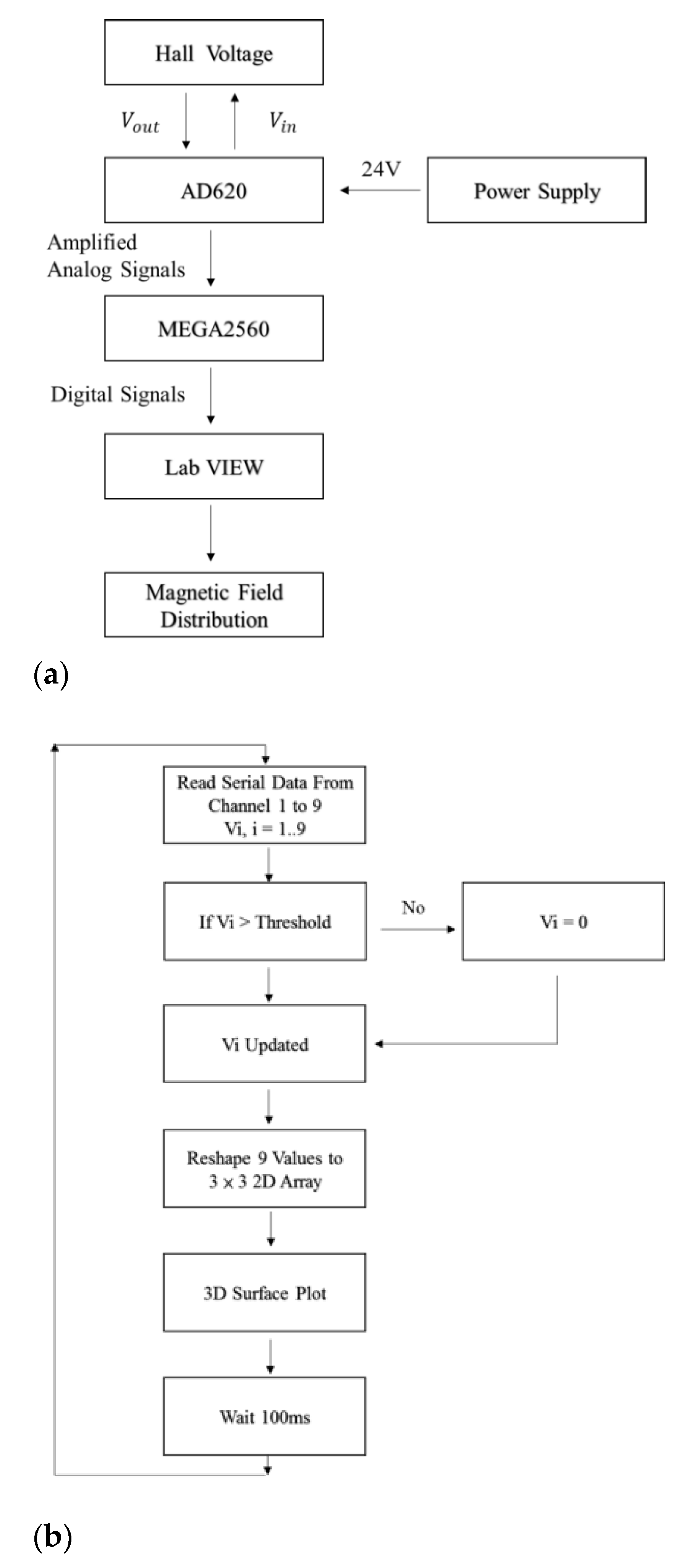
2. Principle and Design
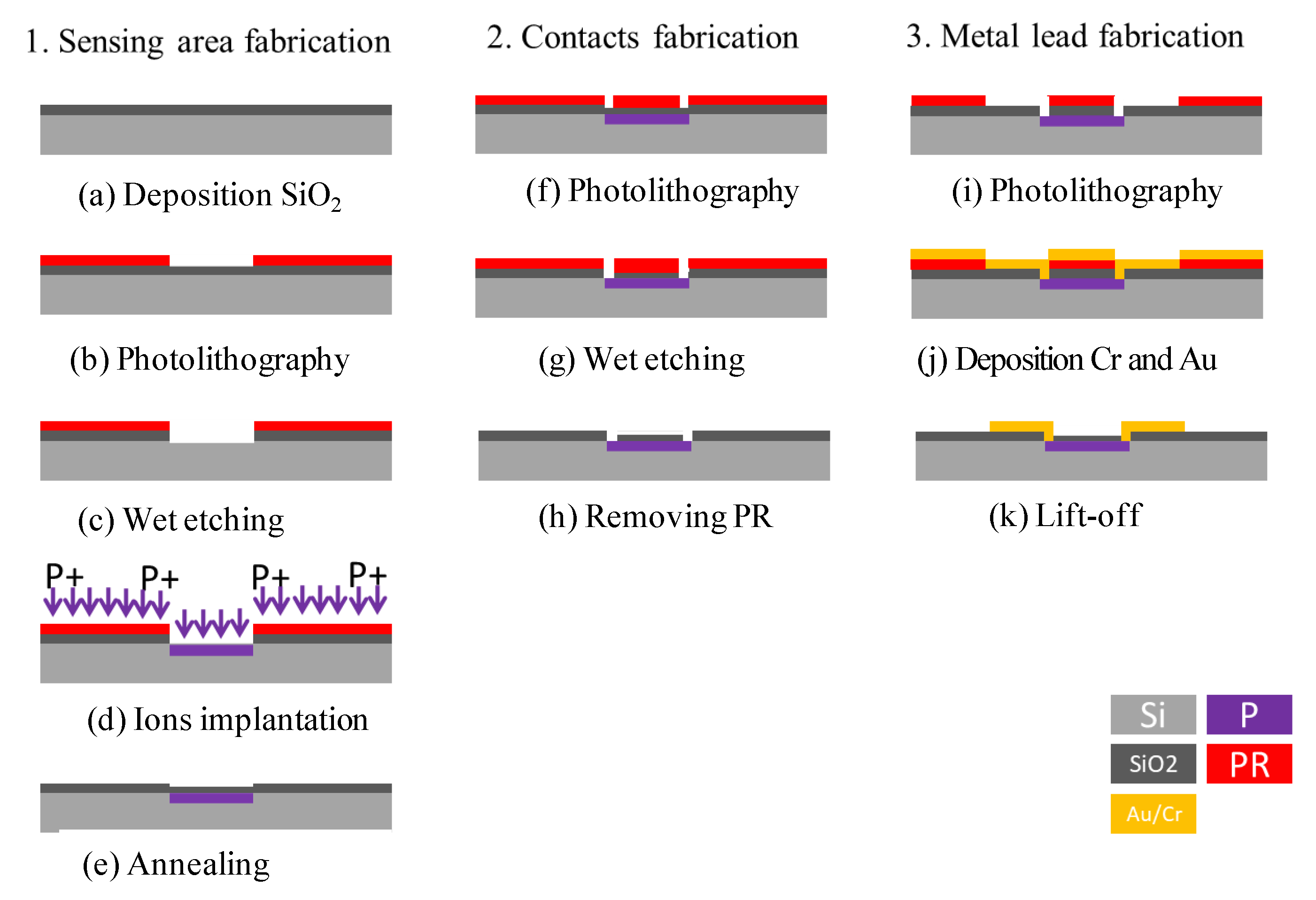
When a current passing through a semiconductor material flows in a direction perpendicular to that of an external magnetic field, the carriers in the semiconductor are deflected to one side and produce a potential difference called the Hall voltage with a magnitude equal to:
V H = I   ×   B   ×   R H d
where I is the electrical current, B is the magnetic field strength, d is the thickness of the semiconductor material and R H = r H nq is the so-called Hall resistivity, in which n is the density of the charge carriers, q is the carrier charge, and r H is the Hall scattering factor depending on the used semiconductor material and the dominant charge carrier mechanism.
Figure 2 presents a schematic illustration of the sensor proposed in the present study consisting of a 4-inch silicon wafer, a silicon dioxide insulating layer, metal leads, and a cross-shaped phosphide-doped detection zone [25,26,27] For comparison purposes, four devices are fabricated, in which the cross-shaped detection zones have the same aspect ratio (L/W = 2.625), but different sizes, namely S, M, L, and XL. In the proposed devices, the analog signals are amplified by a large-current operational amplifier (AD620) and then supplied to an analog-to-digital converter (MEGA2560). Utilizing interpolation elements to smoothen planar display, the digital signals are then processed in LabVIEW to determine the corresponding magnetic field strength and distribution (Figure 3).

3. Fabrication

Figure 4 presents schematic illustrations showing the basic steps of the sensor fabrication process. At first, a silicon oxide isolation layer with a thickness of 0.5 μm was deposited on the surface of the 4-inch P-type < 100 > Si wafer (Thickness: 525 +/ −25 µm, Internal Resistivity: 1–20 Ω-cm) using a High-Density Plasma Chemical Vapor Deposition (HDPCVD) technique (Figure 4a) [28,29]. A photolithography method was employed to pattern (Figure 4b) and etch the cross-shaped detection zone in the Si substrate (Figure 4c) and the detection zone was then implanted with phosphide ions.
(Doping energy: 100 KeV, Depth: 0.1 µm, Concentration: 1015 ions/cm2) (Figure 4d). The residual photoresist (PR) was then stripped away in acetone solution and an annealing process was performed at 900 °C for 1 min(Figure 4e). Apparently, a thin layer of silicon oxide was oxidized on the detection area. A PR layer was then deposited on the surface of the silicon wafer using the photolithography method [30,31] to pattern (Figure 4f) and etch the contact windows of the leads (Figure 4g) on each branch of the cross-shaped detection zone (Figure 4h). Finally, the Electron Beam Evaporation (EBE) method was used to pattern the sensor surface with Au/Cr leads for electrical connection purposes (Figure 4i–k).
Figure 5a presents a photograph of the complete Hall sensors. The sensors were attached to a glass fiberboard using UV glue and encapsulated in resin. Finally, 2 × 2 pin headers were bonded to the sensors using conductive silver glue to form the final sensor assembly Figure 5b.

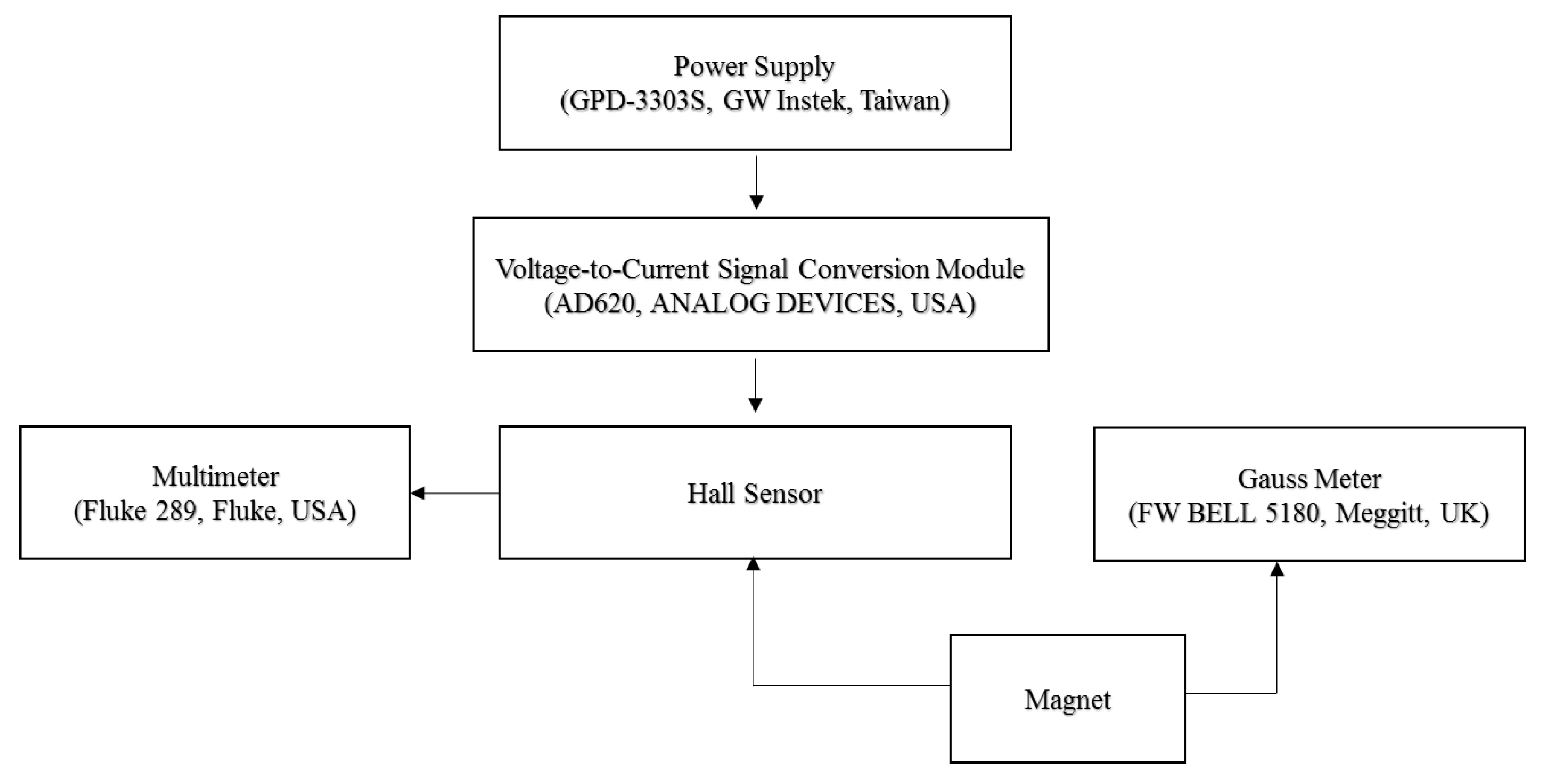
4. Results and Discussion

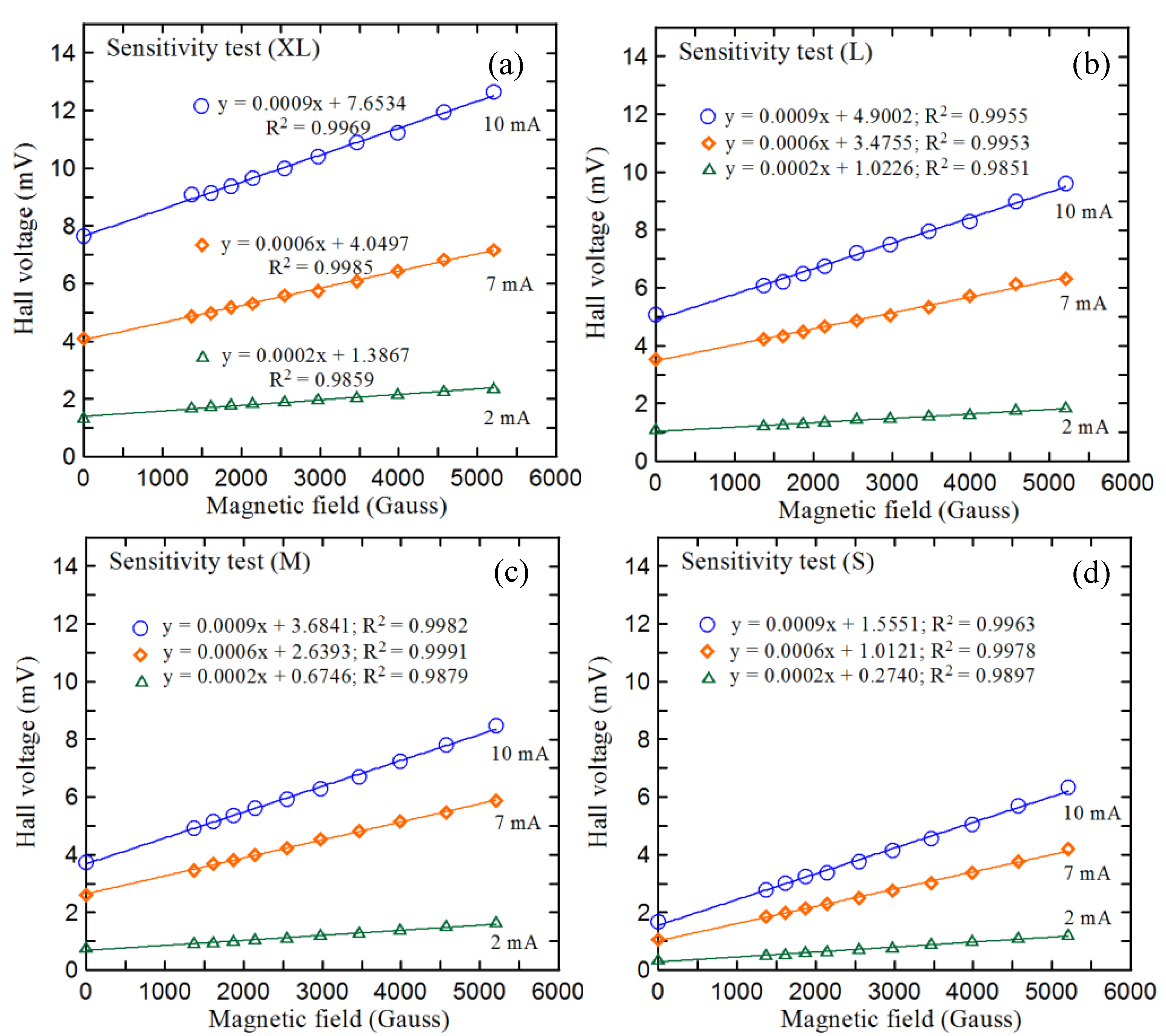
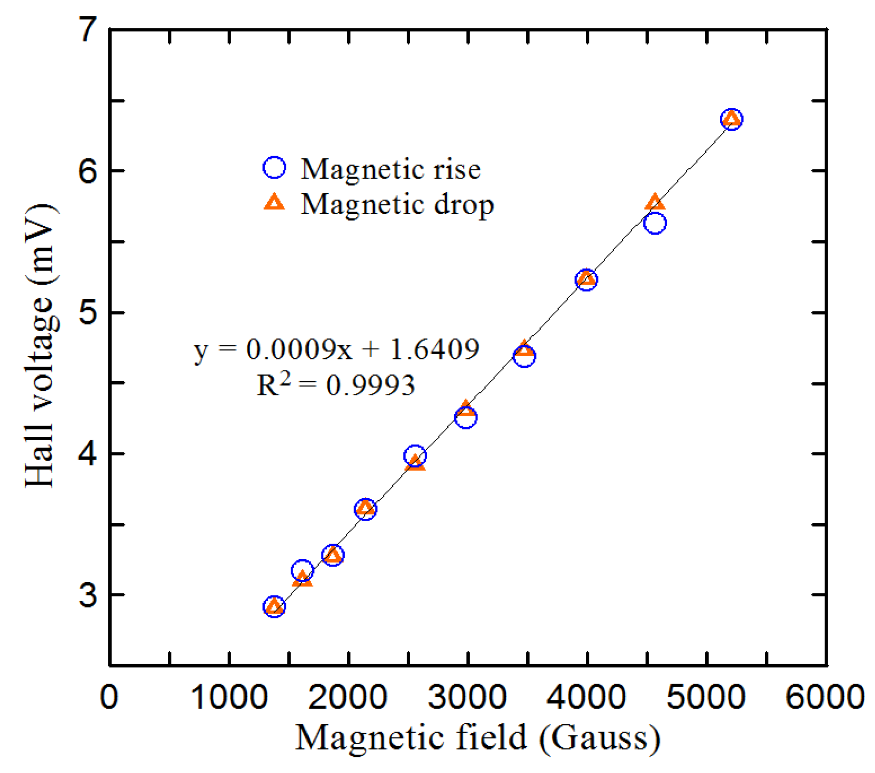
4.1. Sensitivity Test

Figure 6 illustrates the experimental setup used in the present study to characterize and compare the four Hall sensors with different detection zone dimensions. The experiments commenced by measuring the voltage response of the four sensors given different working currents (2, 7, and 10 mA) and magnetic field strengths in the range of 0–5200 Gauss. The corresponding results are presented in Figure 7. As expected, the measured Hall voltages of each sensor increase with the increasing working current. Moreover, for a given working current, the Hall voltage increases linearly with an increasing magnetic field strength (R2 = 0.9955–0.9982). Finally, for a constant magnetic field strength and working current, the Hall voltage increases with an increasing size of the detection zone.
Table 1 compares the sensitivities of the four sizes of devices at each of the considered working currents. It is seen that even though the detection zones in the different devices have different sizes, the devices have the same sensitivity since they conduct the same current in every case. The offset voltage increases with an increasing size of the detection zone at different identical working currents. In other words, the surface electrical properties of the detection zone are more susceptible to the effects of the mechanical stress caused by the manufacturing and packaging processes as the size of the detection zone increases.

4.2. Hysteresis Test

Hysteresis is the time-based dependence of the response on the current and past state of the input. Specifically, the output of the Hall sensor depends not only on the instantaneity of the input but also on its history. If the design is not good enough in the early stages, the hysteresis may make the measurement results different from the previous results [32]. To realize the overall characteristics of the proposed Hall sensor, it is necessary to observe the hysteresis phenomenon under different magnetic fields. The experimental results (Figure 8) show the voltage path used to increase and decrease the magnetic field when the operating current of the Hall sensor of size S is 10 mA. It can be seen that as the magnetic field is less than 4000 Gauss, the two paths are actually almost superimposed. When the magnetic field is greater than 4000 Gauss, the maximum observed hysteresis is 170 Gauss (4.25%). This phenomenon greatly reduces the deviation of the magnetic field measurement, especially at a magnetic field strength less than 4000 Gauss.

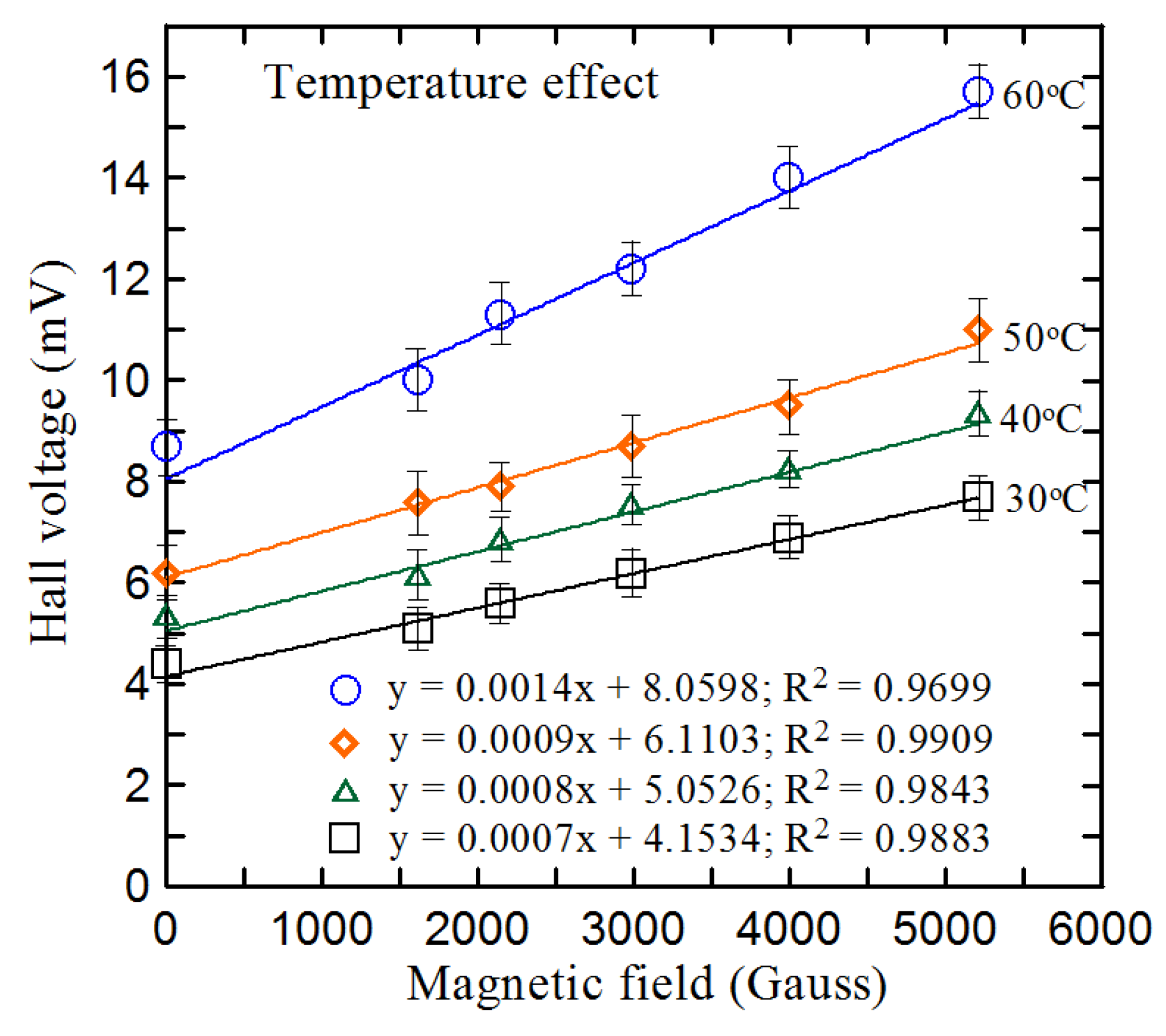
4.3. Temperature Effect Test

One of the key characteristics of the Hall sensor is the effect of offset voltage and sensitivity on temperature. With the advancement of fabrication technology, different offset compensation methods are known, such as calibration, device symmetry, mutual compensation, and reduction of rotating current offset [33,34]. Figure 9 shows the relationship between the offset voltage, sensitivity, and temperature of the S-size Hall sensor when the working current is 10 mA. It can be found that due to the overall temperature coefficient of resistance (TCR) when the ambient temperature is increased from 30 °C to 50 °C at a rate of 0.1 mV/°C, the offset voltage of the Hall sensor increases linearly, and the sensitivity of the sensor also increases with the increase in temperature at a rate of 0.01 µV/Gauss-°C. It is obvious that as the environmental temperature exceeds 50 °C, the offset voltage and sensitivity of the Hall sensor greatly increase due to the greater influence of temperature on the sensor. Temperature compensation can be incorporated according to the results of the temperature effect test for accurate measurement.

4.4. Time Response Test

The responsivity of the four sizes of Hall sensors was evaluated by covering the sensors with a non-metal plate and placing them within a magnetic field with a strength of 2000 Gauss. The plate was abruptly removed from the Hall sensors and the corresponded Hall voltages were recorded. In Figure 10, it is seen that the response time is 8 ms for all four sizes of devices as the working current was 10 mA.

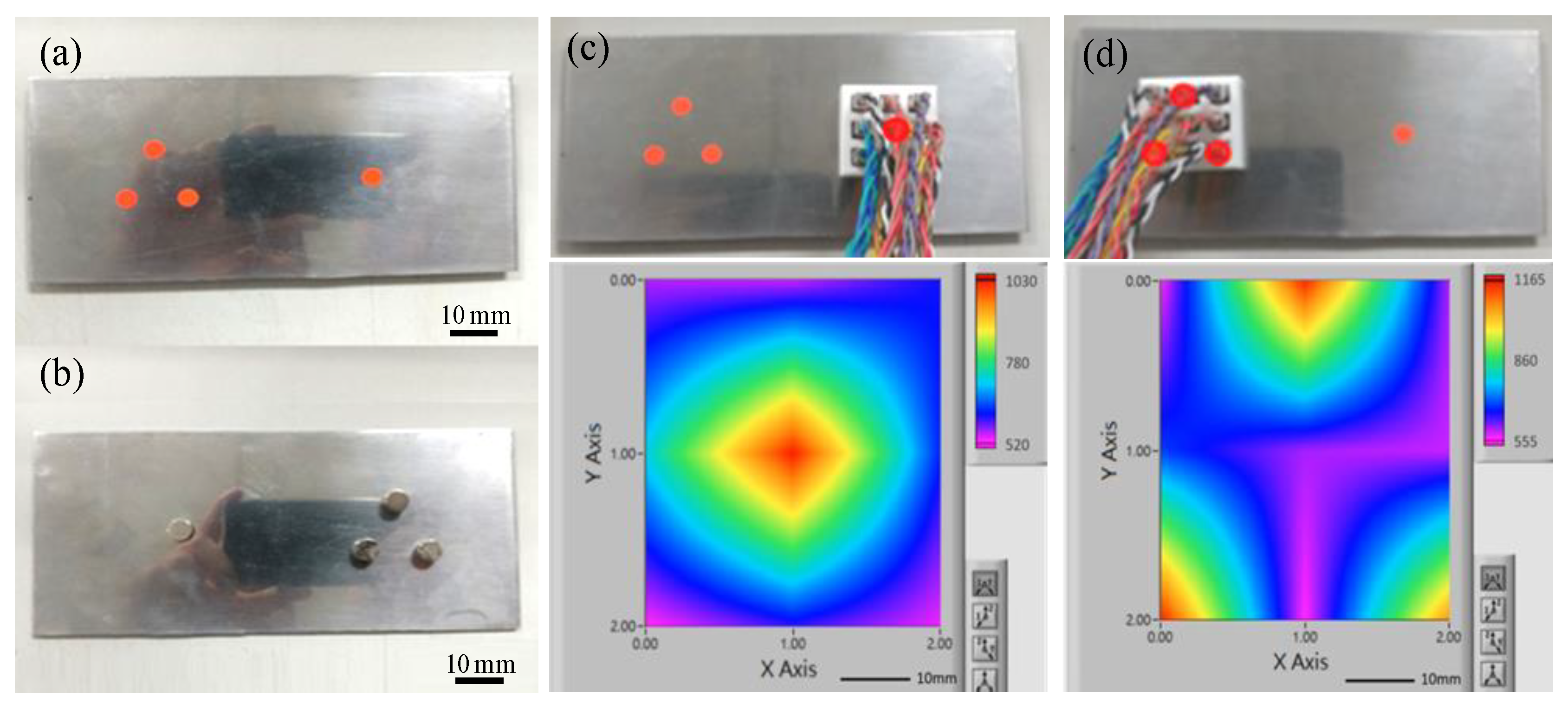
4.5. Integration Test

Having characterized the sensing performance of the proposed Hall sensors, nine sensors were assembled into a 3D-printed plastic frame to create a 3 × 3 sensing array (Figure 11). The size of utilized sensors is S, and the working current is 10 mA. The feasibility of the sensing array was investigated by detecting the magnetic field distributions of a single magnet and a group of three magnets attached to the underside of an iron plate, respectively (Figure 12a,b). The magnetic field strength of each circle magnet (Diameter: 18 mm, Thickness: 5 mm) is 1420 Gauss. The detection results are presented in Figure 12c,d respectively. It is seen that for both arrangements of the magnets, the 2D magnetic field contour maps constructed in LabView accurately detect both the locations of the individual magnets and the distributions of the magnetic fields around them. The operational video is attached.

5. Conclusions

This study has designed and fabricated Hall sensors with application to magnetic field strength measurement. On a P-type silicon substrate, the device features a phosphide-doped cross-shaped detection zone and is fabricated using simple MEMS-based techniques, including HDPCVD sputtering, photolithography patterning, ion implantation, and EBE metal lead deposition. Four kinds of devices have been constructed with detection zones of identical aspect ratio (2.625) but different sizes (S, M, L, and XL). The experimental results have shown that all four sizes of devices have a linear response over the range of 0–5200 Gauss for working currents of 2 mA, 7 mA, and 10 mA. For a constant working current, the four sensors have an identical sensitivity and a similar response time (8 ms) despite the difference in the size of the detection zone. However, the offset voltage increases with an increasing detection zone size; indicating that the surface electrical properties of the detection zone are more susceptible to the effects of the manufacturing and packaging processes as the size of the detection zone increases. The practical feasibility of the proposed sensors has been demonstrated by measuring the magnetic field mapping of a single magnet and a group of three magnets, respectively, using a 3 × 3 array of sensors assembled into a 3D-printed frame, which will be an important tool in the NDT field.

Author Contributions

L.-M.F. and C.-Y.L. conceived and designed the experiments; Y.-Y.L. and C.-K.K. performed the experiments; L.-M.F. and C.-Y.L. analyzed the data; Y.-Y.L. and C.-K.K. contributed reagents/materials/analysis tools; Y.-Y.L., L.-M.F. and C.-Y.L. wrote the paper. All authors have read and agreed to the published version of the manuscript.

Funding

This research was funded by the Ministry of Science and Technology in Taiwan, grant number MOST 108-2622-E-020-004-CC3; MOST 108-2622-E-006-026-CC2, and MOST 109-2221-E-006-043-MY3.

Institutional Review Board Statement

Not applicable.

Informed Consent Statement

Not applicable.

Data Availability Statement

The data presented in this study are available on request from the corresponding author.

Conflicts of Interest

The authors declare no conflict of interest.

References

  1. Zhang, Y.; Hao, Q.; Xiao, G. Low-frequency noise of magnetic sensors based on the anomalous Hall effect in Fe–Pt alloys. Sensors 2019, 19, 3537. [Google Scholar] [CrossRef] [Green Version]
  2. Lin, Y.N.; Dai, C.L. Micro magnetic field sensors manufactured using a standard 0.18-μm CMOS process. Micromachines 2018, 9, 393. [Google Scholar] [CrossRef] [Green Version]
  3. Fujiwara, K.; Satake, Y.; Shiogai, J.; Tsukazaki, A. Doping-induced enhancement of anomalous Hall coefficient in Fe-Sn nanocrystalline films for highly sensitive Hall sensors. APL Mater. 2019, 7, 111103. [Google Scholar] [CrossRef]
  4. Collomb, D.; Li, P.; Bending, S.J. Nanoscale graphene Hall sensors for high-resolution ambient magnetic imaging. Sci. Rep. 2019, 9, 14424. [Google Scholar] [CrossRef] [Green Version]
  5. Xuan, X. Recent advances in continuous-flow particle manipulations using magnetic fluids. Micromachines 2019, 10, 744. [Google Scholar] [CrossRef] [Green Version]
  6. Stern, M.; Cohen, M.; Danielli, A. Configuration and design of electromagnets for rapid and precise manipulation of magnetic beads in biosensing applications. Micromachines 2019, 10, 784. [Google Scholar] [CrossRef] [Green Version]
  7. Li, X.; Fukuda, T. Magnetically guided micromanipulation of magnetic microrobots for accurate creation of artistic patterns in liquid environment. Micromachines 2020, 11, 697. [Google Scholar] [CrossRef]
  8. Lee, S.; Hong, S.; Park, W.; Kim, W.; Lee, J.; Shin, K.; Kim, C.; Lee, D. High accuracy open-type current sensor with a differential planar Hall resistive sensor. Sensors 2018, 18, 2231. [Google Scholar] [CrossRef] [PubMed] [Green Version]
  9. Fan, L.; Bi, J.; Xi, K.; Yan, G. Investigation of radiation effects on FD-SOI Hall sensors by TCAD simulations. Sensors 2020, 20, 3946. [Google Scholar] [CrossRef]
  10. Yatchev, I.; Sen, M.; Balabozov, I.; Kostov, I. Modelling of a Hall effect-based current sensor with an open core magnetic concentrator. Sensors 2018, 18, 1260. [Google Scholar] [CrossRef] [Green Version]
  11. Petruk, O.; Kachniarz, M.; Szewczyk, R. Novel method of offset voltage minimization in hall-effect sensor. Acta Phys. Pol. A 2017, 131, 1177. [Google Scholar] [CrossRef]
  12. Lin, C.H. Precision motion control of a linear permanent magnet synchronous machine based on linear optical-ruler sensor and Hall sensor. Sensors 2018, 18, 3345. [Google Scholar] [CrossRef] [Green Version]
  13. Roy, A.; Sampathkumar, P.; Kumar, P.S.A. Development of a very high sensitivity magnetic field sensor based on planar Hall effect. Measurement 2020, 156, 107590. [Google Scholar] [CrossRef]
  14. Liang, C.; Zhang, Y.; Li, Z.; Yuan, F.; Yang, G.; Song, K. Coil positioning for wireless power transfer system of automatic guided vehicle based on magnetic sensing. Sensors 2020, 20, 5304. [Google Scholar] [CrossRef]
  15. Ursel, T.; Olinski, M. Displacement estimation based on optical and inertial sensor fusion. Sensors 2021, 21, 1390. [Google Scholar] [CrossRef]
  16. Martinez-Garcia, M.; Zhang, Y.; Wan, J.; McGinty, J. Visually interpretable profile extraction with an autoencoder for health monitoring of industrial systems. In Proceedings of the 2019 IEEE 4th International Conference on Advanced Robotics and Mechatronics (ICARM), Osaka, Japan, 3–5 July 2019. [Google Scholar]
  17. Martinez-Garcia, M.; Zhang, Y.; Suzuki, K.; Zhang, Y.-D. Deep recurrent entropy adaptive model for system reliability monitoring. IEEE Trans. Ind. Inform. 2020, 17, 839. [Google Scholar] [CrossRef]
  18. Lozanova, S.; Ivanov, A.; Roumenin, C. A novel three-axis hall magnetic sensor. Procedia Eng. 2011, 25, 539–542. [Google Scholar] [CrossRef] [Green Version]
  19. Lozanova, S.; Noykov, S.; Roumenin, C. Two-axis silicon hall effect magnetometer. Sens. Actuators A Phys. 2017, 267, 177–181. [Google Scholar] [CrossRef]
  20. Zhao, B.; Shi, W.J.; Zhang, J.W.; Zhang, M.; Qi, X.; Li, J.X.; Tan, J.B. Six degrees of freedom displacement measurement system for wafer stage composed of Hall sensors. Sensors 2018, 18, 2030. [Google Scholar] [CrossRef] [Green Version]
  21. Xu, H.; Zhang, Z.; Shi, R.; Liu, H.; Wang, Z.; Wang, S.; Peng, L.M. Batch-fabricated high-performance graphene Hall elements. Sci. Rep. 2013, 3, 1207. [Google Scholar] [CrossRef]
  22. Jones, D.; Wang, L.; Ghanbari, A.; Vardakastani, V.; Kedgley, A.E.; Gardiner, M.D.; Vincent, T.L.; Culmer, P.R.; Alazmani, A. Design and evaluation of magnetic Hall effect tactile sensors for use in sensorized splints. Sensors 2020, 20, 1123. [Google Scholar] [CrossRef] [Green Version]
  23. Berus, T.; Oszwaldowski, M.; Grabowski, J. High quality Hall sensors made of heavily doped n-InSb epitaxial films. Sens. Actuators A Phys. 2004, 116, 75–78. [Google Scholar] [CrossRef]
  24. Uzlu, B.; Wang, Z.; Lukas, S.; Otto, M.; Lemme, M.C.; Neumaier, D. Gate-tunable graphene-based Hall sensors on flexible substrates with increased sensitivity. Sci. Rep. 2019, 9, 18059. [Google Scholar] [CrossRef]
  25. Jovanovic, E.; Pesic, T.; Pantic, D. 3D simulation of cross-shaped hall sensor and its equivalent circuit model. In Proceedings of the 24th International Conference on Microelectronics (MIEL), Niš, Serbia, 16–19 May 2004; pp. 235–238. [Google Scholar]
  26. Wei, R.; Du, Y. Analysis of orthogonal coupling structure based on double three-contact vertical hall device. Micromachines 2019, 10, 610. [Google Scholar] [CrossRef] [PubMed] [Green Version]
  27. Fan, L.; Bi, J.; Xi, K.; Majumdar, S.; Li, B. Performance optimization of FD-SOI hall sensors via 3D TCAD simulations. Sensors 2020, 20, 2751. [Google Scholar] [CrossRef] [PubMed]
  28. Kim, Y.; Lee, M.; Kim, Y.J. Selective growth and contact gap-fill of low resistivity Si via microwave plasma-enhanced CVD. Micromachines 2019, 10, 689. [Google Scholar] [CrossRef] [Green Version]
  29. Fraga, M.; Pessoa, R. Progresses in synthesis and application of SiC Films: From CVD to ALD and from MEMS to NEMS. Micromachines 2020, 11, 799. [Google Scholar] [CrossRef]
  30. Lee, A.H.; Lee, J.; Laiwalla, F.; Leung, V.; Huang, J.; Nurmikko, A.; Song, Y.K. A scalable and low stress post-CMOS processing technique for implantable microsensors. Micromachines 2020, 11, 925. [Google Scholar] [CrossRef]
  31. Puryear, J.R.; Yoon, J.; Kim, Y.T. Advanced fabrication techniques of microengineered physiological systems. Micromachines 2020, 11, 730. [Google Scholar] [CrossRef] [PubMed]
  32. Nguyen, P.B.; Choi, S.B.; Song, B.K. A new approach to hyeteresis modelling for a piezoelectric actuator using Preisach model and recursive method with an application to open-loop position tracking control. Sens. Actuators A Phys. 2018, 270, 136. [Google Scholar] [CrossRef]
  33. Cholakova, I.M.; Takov, T.B.; Tsankov, R.T.; Simonne, N. Temperature influence on Hall sensors characteristics. In Proceedings of the 20th Telecommunications Forum TELFOR, Belgrade, Serbia, 20–22 November 2012; p. 967. [Google Scholar]
  34. Tang, W.; Lyu, F.; Wang, D.; Pan, H. A new design of a single-device 3D Hall sensor: Cross-shaped 3D Hall sensor. Sensors 2018, 18, 1065. [Google Scholar] [CrossRef] [PubMed] [Green Version]
Figure 1. Schematic illustration of Hall effect.
Micromachines 12 00299 g001
Figure 2. Schematic illustration of Hall sensor design and dimensions of four sizes of cross-shaped detection zones.
Micromachines 12 00299 g002
Figure 3. Block diagrams showing (a) analog circuit and signal conversion path of proposed Hall sensor array and (b) LabVIEW program of the visualization platform of the magnetic field mapping.
Micromachines 12 00299 g003
Figure 4. Schematic illustration showing the main steps of the fabrication process of Hall sensor: (a) deposition of SiO2, (b) photolithography, (c) wet etching, (d) ion implantation, (e) annealing, (f) photolithography, (g) wet etching, (h) removing PR, (i) photolithography, (j) deposition of Cr and Au, and (k) lift-off.
Micromachines 12 00299 g004
Figure 5. Photographs of: (a) complete Hall sensor, and (b) resin-encapsulation of individual Hall sensor.
Micromachines 12 00299 g005
Figure 6. Experimental setup.
Micromachines 12 00299 g006
Figure 7. Sensitivity results for Hall sensors of size (a) XL, (b) L, (c) M, and (d) S.
Micromachines 12 00299 g007
Figure 8. Magnetic hysteresis curve for the Hall sensor of size S at 10 mA of working current.
Micromachines 12 00299 g008
Figure 9. Temperature effect on voltage offset and sensitivity of the S-sized hall sensors at 30 °C, 40 °C, 50 °C, and 60 °C as the working current is 10 mA.
Micromachines 12 00299 g009
Figure 10. Time responses of Hall sensors of various sizes: (a) S, (b) M, (c) L, and (d) XL.
Micromachines 12 00299 g010
Figure 11. Photographs of: (a) 3D-printed Hall sensor frame, and (b) 3 × 3 Hall sensor array consisting of 9 sensing modules.
Micromachines 12 00299 g011
Figure 12. Photographs of: (a,b) front and rear sides of the iron plate with attached magnets; (c,d) single magnet and three-magnet detection arrangements and corresponded 2D magnetic field distributions (unit: Gauss).
Micromachines 12 00299 g012
Table 1. Offset voltage, sensitivity, and coefficients of determination of four sizes of Hall sensors under three different working currents.
XLLMS
working current
10 mA
offset voltage (mV)7.6405.0633.7441.668
sensitivity
(μV/Gauss)
0.9230.9140.9300.909
R-square0.99690.99550.99820.9963
working current
7 mA
offset voltage (mV)4.0833.5412.6131.056
sensitivity
(μV/Gauss)
0.6150.6210.5980.607
R-square0.99850.99530.99910.9978
working current
2 mA
offset voltage (mV)1.3021.0690.7370.330
sensitivity
(μV/Gauss)
0.2140.1960.2310.208
R-square0.98590.98510.98790.9897
Publisher’s Note: MDPI stays neutral with regard to jurisdictional claims in published maps and institutional affiliations.

